Soft Error Analysis and Mitigation In Circuits Involving C … · · 2016-06-01... Truth Table...
235
i Soft Error Analysis and Mitigation In Circuits Involving C-Elements A Thesis Presented to Newcastle University by NORHUZAIMIN BIN JULAI In Partial Fulfilment of the Requirement for the Degree of Doctor of Philosophy in Electrical and Computer Engineering School of Electrical, Electronic and Computer Engineering University of Newcastle
Transcript of Soft Error Analysis and Mitigation In Circuits Involving C … · · 2016-06-01... Truth Table...
i
Soft Error Analysis and Mitigation
In Circuits Involving C-Elements
A Thesis Presented to
Newcastle University by
NORHUZAIMIN BIN JULAI
In Partial Fulfilment
of the Requirement for the Degree of
Doctor of Philosophy in Electrical and Computer Engineering
School of Electrical, Electronic and Computer Engineering
University of Newcastle

ii
iii
CONTENTS
Contents………………………………………………………………...
iii
List of Algorithms/Tables……………………………………………..
vii
List of Figures…………………………………………………………
viii
Abstract………………………………………………………………...
xviii
Glossary…………………………………………………………………
xix
Acknowledgement……………………………………………………
xxi
Chapter 1 Introduction………………………………………………
1
1.1 Motivation………………………………………………………..
1
1.2 Objectives………………………………………………………..
4
1.3
Thesis Overview…………………………………………………. 5
1.4 Thesis Contributions……………………………………………..
6
1.5 Publications……………………………………………………….
7
Chapter 2 Basics Concepts…………………………………………..
8
2.1 Radiation Effects in Digital Systems……………………………..
8
2.1.1 Sources of Radiations…………………………………….
8
2.1.2 The Effects of Radiation…………………………………
10
2.1.3 Single Event Upset Modelling…………………………..
13
2.2 Asynchronous Design……………………………………………
16
2.2.1 Advantages of Asynchronous Design……………………
16
2.2.2 C-element……………………………………………….. 17
2.2.3 Classification of Asynchronous Circuit…………………
18
2.2.4 Asynchronous Circuit Implementation…………………
19
2.3 Dual Rail Data……………………………………………………
21
2.3.1 Dual Rail Data Encoding………………………………..
21
2.3.2 Handshake Protocols……………………………………
22
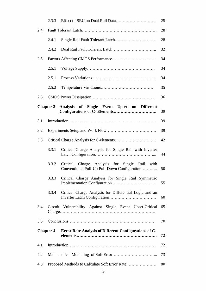
iv
2.3.3 Effect of SEU on Dual Rail Data………………………...
25
2.4 Fault Tolerant Latch………………………………………………
28
2.4.1 Single Rail Fault Tolerant Latch…………………………
28
2.4.2 Dual Rail Fault Tolerant Latch…………………………..
32
2.5 Factors Affecting CMOS Performance…………………………..
34
2.5.1 Voltage Supply………………………………………….
34
2.5.1 Process Variations……………………………………….
34
2.5.2 Temperature Variations…………………………………
35
2.6 CMOS Power Dissipation……………………………………….
36
Chapter 3 Analysis of Single Event Upset on Different
Configurations of C- Elements………………………….
39
3.1 Introduction…….…………………………………………………
39
3.2 Experiments Setup and Work Flow………………………………
39
3.3 Critical Charge Analysis for C-elements…………………………
42
3.3.1 Critical Charge Analysis for Single Rail with Inverter
Latch Configuration……………………………………...
44
3.3.2 Critical Charge Analysis for Single Rail with
Conventional Pull-Up Pull-Down Configuration………...
50
3.3.3 Critical Charge Analysis for Single Rail Symmetric
Implementation Configuration…………………………..
55
3.3.4 Critical Charge Analysis for Differential Logic and an
Inverter Latch Configuration…………………………….
60
3.4 Circuit Vulnerability Against Single Event Upset-Critical
Charge…………………………………………………………….
65
3.5 Conclusions………………………………………………………
70
Chapter 4 Error Rate Analysis of Different Configurations of C-
elements………………………………………………….
72
4.1 Introduction………………………………………………………
72
4.2 Mathematical Modelling of Soft Error…………………………...
73
4.3 Proposed Methods to Calculate Soft Error Rate ………………… 80
v
4.4 Result And Analysis………………………………………………
84
4.4.1 Error Rate for Single Rail with Inverter Latch
Configuration…………………………………………….
84
4.4.2 Error Rate for Single Rail with Conventional Pull-Up
Pull-Down Configuration………………………………
94
4.4.3 Error Rate for Single Rail Symmetric Implementation
Configuration……………………………………………
103
4.4.4 Error Rate for Differential Logic and an Inverter Latch
Configuration……………………………………………
111
4.5 Circuit Vulnerability Against Single Event Upset -Error Rate…..
120
4.5.1 Error Rate Comparison………………………………….
121
4.5.2 Sensitivity Analysis……………………………………..
122
4.6 Conclusions………………………………………………………
125
Chapter 5 Error Detection and Correction of Single Event Upset
Tolerant Latch for Single Rail Data…………………
127
5.1 Introduction………………………………………………………
127
5.2 Proposed Error Detection Latch……….…………………………
128
5.3 Proposed Error Detection and Correction Latch…………………
139
5.4 Implementation of Full Adder System by using Error Detection
and Correction Latch……………………………………………
152
5.5 Conclusions………………………………………………………
155
Chapter 6 Error Detection and Correction of Single Event Upset
Tolerant Latch for Dual Rail Data……………………
156
6.1 Introduction………………………………………………………
156
6.2 Proposed Error Detection for Dual Rail Data …………………...
156
6.3 Proposed Error Detection and Correction for Dual Rail Data …...
166
6.4 Proposed Error Detection and Correction for Dual Rail data with
Transient Correction Latch…...…………………………………
179
6.5 Conclusions………………………………………………………
186
vi
Chapter 7 The design of Asynchronous On-chip Communication
by using EDCD Proposed Latch……………………….
187
7.1 Introduction………………………………………………………
187
7.2 Asynchronous on-chip communication by using EDCD Latch… 187
7.3 Result and Simulation Employing EDCD Latch…………………
193
7.4 Conclusions………………………………………………………
196
Chapter 8 Conclusions And Future Works………………………..
197
8.1 Conclusions………………………………………………………
197
8.2 Future Works……………………………………………………..
198
Appendixes……………………………………………………………..
200
References………………………………………………………………
209
vii
List of Algorithms/Tables
Table 1: Ground Level Soft Error Rates Measured by RAM………….. 2
Table 2: Dual Rail Encoding………………………………………… 21
Method 4.1: Calculate the critical charge and normalized cross section
of NMOS/PMOS with neutron…………………………………………
80
Method 4.2: Calculate charge, energy and rate of error with amplitude
less than 380……………………………………………………………
81
Method 4.3: Calculate charge, energy and rate of error with amplitude
more than 380………………………………………………………….
82
Method 4.4: Calculate error rate……………………………………… 83
Table 4.1: Standard Deviation for the Process Corner-SIL…………… 86
Table 4.2: Standard Deviation for the Process Corner-SC…………… 95
Table 4.3: Standard Deviation for the Process Corner-SS…………… 104
Table 4.4: Standard Deviation for the Process Corner-DIL…………… 113
Table 5.1:Vulnerables nodes on converter…………………………… 129
Table 5.2: Vulnerable nodes on ED Latch…………………………… 139
Table 5.3: Vulnerable nodes on EDC Latch………………………… 149
Table 5.4: Propagation Delay Between ED And EDC Latch………… 151
Table 5.5: Switching Power Between ED And EDC Latch…………… 152
Table 5.6: Truth Table Full Adder…………………………………… 153
Table 6.1: Vulnerable nodes on EDD Latch…………………………… 165
Table 6.2: Vulnerable nodes on EDCD Latch………………………… 177
Table 6.3: Propagation Delay Comparison…………………………… 178
Table 6.4: Switching Power Comparison……………………………… 179
Table 6.5: Comparison of Different Latches………………………… 186
Table 6.6: Comparison of Different Latches………………………… 186
Algorithm 7.1. VHDL for C-element………………………………… 188
Algorithm 7.2. VHDL for Shadow Latch …………………………… 188
Table 7.1: Code comparison in terms of wires, transition and capacity.. 190
Table 7.2: Interface of dual rail to 3-6 and back to dual rail conversion. 192
Table 7.3: 3-6 and dual rail code……………………………………… 193
Table 1B: Interface of Adder System…………………………………. 203
Algorithm 1: Brent Kung 8-Bit Adder………………………………… 207
viii
List of Figures
Figure 1: The evolution of transistors with respect to year……………. 1
Figure 2.1: Neutron energy spectrum………………………………….. 9
Figure 2.2: Interaction of Boron and neutron…………………………. 10
Figure 2.3: Neutron spectrum below 1 MeV, including thermal-energy
neutrons………………………………………………………………...
10
Figure 2.4: SEU produced …………………………………………….. 11
Figure 2.5: The drain current versus the gate voltage for MOSFET…... 13
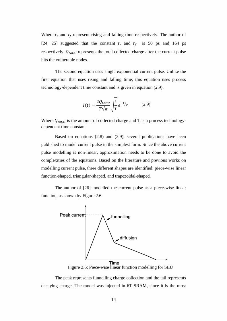
Figure 2.6: Piece-wise linear function modelling for SEU……………. 14
Figure 2.7: Triangular-shaped modelling for SEU…………………… 15
Figure 2.8: Trapezoidal-shaped SEU………………………………… 15
Figure 2.9: (a) Muller C-element (b) Asymmetric C-element (c)
Asymmetric C-element…………………………………………………
18
Figure 2.10: Asynchronous buffer implementation ………...…………. 19
Figure 2.11: Asynchronous implementation…………………………... 20
Figure 2.12: Multiplexer ……………………………………................. 20
Figure 2.13: Dual Rail And Gate……………………………………… 22
Figure 2.14: Muller Pipeline Latch…………………………………… 22
Figure 2.15: 4-phase dual rail protocol………………………………… 23
Figure 2.16: 2-phase dual rail protocol………………………………… 23
Figure 2.17: 4-phase bundle pipeline………………………………… 24
Figure 2.18: 2-phase bundle pipeline………………………………… 24
Figure 2.19: 2-phase pipeline “Mousetrap”…………………………… 25
Figure 2.20: Fault Free 1-bit Dual Rail……………………………… 26
Figure 2.21: Case 1: 1-bit Dual Rail Pipeline………………………… 27
Figure 2.22: Case 2: 1-bit Dual Rail Pipeline………………………… 27
Figure 2.23: Case 3: 1-bit Dual Rail Pipeline………………………… 28
Figure 2.24: FERST…………………………………………………… 29
Figure 2.25: SIN-LC ………………………………………………… 30
Figure 2.26: SIN-HR………………………………………………… 30
Figure 2.27: SDT…………………………………………………… 30
Figure 2.28: (a) BISER (b) BISER with duplication (c) BISER with
time delay (d) C-element used in BISER………………………………
32
Figure 2.29: Duplication Latch………………………………………… 32
Figure 2.30: Rail synchronization latch……………………………… 33
Figure 3.1: SEU Current Modelling…………………………………… 40
Figure 3.2: Workflow of the experiments…………………………… 42
Figure 3.3: SIL Configuration………………………………………… 44
Figure 3.4(a): Process Corner Variation for SIL configuration (A=1,
B=0)…………………………………………………………………….
46
Figure 3.4(b): Process Corner Variation for SIL configuration (A=0,
B=1)…………………
46
Figure 3.5(a): Temperature Variation for SIL configuration (A=1,
B=0)…………………………………………………………………….
47
Figure 3.5(b): Temperature Variation for SIL configuration (A=0,
B=1)……………………………………………………….
47
Figure 3.6(a): Voltage and Size Scaling for SIL configuration (A=1,
B=0)…….................................................................................................
49
Figure 3.6(b): Voltage and Size Scaling for SIL configuration (A=0,
B=1)……................................................................................................
49
Figure 3.7(a): Voltage Supply Scaling for SIL configuration (A=1, 50
ix
B=0)……….............................................................................................
Figure 3.7(b): Voltage Supply Scaling for SIL configuration (A=0,
B=1)……….............................................................................................
50
Figure 3.8(a): Size Scaling for SIL configuration (A=1,
B=0)…………………………………………………………………….
50
Figure 3.9: SC configuration…………………………………………... 51
Figure 3.10(a): Process Corner Variation for SC configuration (A=1,
B=0)……………………………………………………………………
53
Figure 3.10(b): Process Corner Variation for SC configuration (A=0,
B=1)…………………………………………………………………….
53
Figure 3.11(a): Temperature Variation for SC configuration (A=1,
B=0)………….
53
Figure 3.11(b): Temperature Variation for SC configuration (A=0,
B=1)…………………………………………………………………….
53
Figure 3.12(a): Voltage and Size Scaling for SC configuration (A=1,
B=0)…………………………………………………………………….
54
Figure 3.12(b): Voltage and Size Scaling for SC configuration (A=0,
B=1)………
54
Figure 3.13(a): Voltage Supply Scaling for SC configuration (A=1,
B=0)………....
54
Figure 3.13(b): Voltage Supply Scaling for SC configuration (A=0,
B=1)……….............................................................................................
54
Figure 3.14(a): Size Scaling for SC configuration (A=1,
B=0)……………………..
55
Figure 3.14(b): Size Scaling for SC configuration (A=0,
B=1)…………………………………………………………………….
55
Figure 3.15: SS configuration…………………………………………. 56
Figure 3.16(a): Process Corner Variation for SS configuration (A=1,
B=0)…………………………………………………………………….
58
Figure 3.16(b): Process Corner Variation for SS configuration (A=0,
B=1)…………………………………………………………………….
58
Figure 3.17(a): Temperature Variation for SS configuration (A=1,
B=0)…………………………………………………………………….
58
Figure 3.17(b): Temperature Variation for SS configuration (A=0,
B=1)…………………………………………………………………….
58
Figure 3.18(a): Voltage and Size Scaling for SS configuration (A=1,
B=0)…………………………………………………………………….
59
Figure 3.18(b): Voltage and Size Scaling for SS configuration (A=0,
B=1)…………………………………………………………………….
59
Figure 3.19(a): Voltage Supply Scaling for SS configuration (A=1,
B=0)…………………………………………………………………….
59
Figure 3.19(b): Voltage Supply Scaling for SS configuration (A=0,
B=1)……….............................................................................................
59
Figure 3.20(a): Size Scaling for SS configuration (A=1, B=0)……….. 60
Figure 3.20(b): Size Scaling for SS configuration (A=0, B=1)……….. 60
Figure 3.21: DIL configuration……………………………………….. 61
Figure 3.22(a): Process Corner Variation for DIL configuration (A=1,
B=0)…….................................................................................................
63
Figure 3.22(b): Process Corner Variation for DIL configuration (A=0,
B=1)……................................................................................................
63
Figure 3.23(a): Temperature Variation for DIL configuration (A=1,
B=0)…………………………………………………………………….
63
x
Figure 3.23(b): Temperature Variation for DIL configuration (A=0,
B=1)……….............................................................................................
63
Figure 3.24(a): Voltage and Size Scaling for DIL configuration (A=1,
B=0)……....
64
Figure 3.24(b): Voltage and Size Scaling for DIL configuration (A=0,
B=1)……....
64
Figure 3.25(a): Voltage Supply Scaling for DIL configuration (A=1,
B=0)…………………………………………………………………….
64
Figure 3.25(b): Voltage Supply Scaling for DIL configuration (A=0,
B=1)………..
64
Figure 3.26(a): Size Scaling for DIL configuration (A=1,
B=0)…………………………………………………………………….
65
Figure 3.26(b): Size Scaling for DIL configuration (A=0,
B=1)…………………………………………………………………….
65
Figure 3.27(a): Comparison of Standard Deviation with respect to
Process Corner (A=1, B=0)…………………………………………….
66
Figure 3.27(b): Comparison of Standard Deviation with respect to
Process Corner (A=0, B=1) ……………………………………………
67
Figure 3.28(a): Comparison of Standard Deviation with respect to
Temperature (A=1, B=0)………………………………………………
67
Figure 3.28(b): Comparison of Standard Deviation with respect to
Temperature (A=0, B=1)………………………………………………
68
Figure 3.29(a): Comparison of Standard Deviation with respect to
Voltage and Scaling (A=1, B=0)………………………………………
68
Figure 3.29(b): Comparison of Standard Deviation with respect to
Voltage and Scaling (A=0, B=1)………………………………………
68
Figure 3.30(a): Comparison of Standard Deviation with respect to
Voltage Scaling (A=1, B=0)…………………………………………
69
Figure 3.30(b): Comparison of Standard Deviation with respect to
Voltage Scaling (A=0, B=1)……………………………………………
69
Figure 3.31(a): Comparison of Standard Deviation with respect to Size
Scaling (A=1, B=0)…………………………………………………….
70
Figure 3.31(b): Comparison of Standard Deviation with respect to Size
Scaling (A=0, B=1)…………………………………………………….
70
Figure 4.1: State holder change from low to high (0-1)……………….. 73
Figure 4.2: State holder change from high to low (1-0)……………….. 73
Figure 4.3: Normalized atmospheric neutron cross section with the
drain area……………………………………………………………….
77
Figure 4.4: (a) SIL Configuration (b) Layout SIL Configuration …….. 85
Figure 4.5(a): Error rate due to neutron energy spectrum with respect
to Process Corner-SIL (A=1 B=0)……………………………………..
86
Figure 4.5(b): Error rate due to neutron energy spectrum with respect
to Process Corner-SIL (A=0 B=1)……………………………………..
86
Figure 4.6(a): Total Error rate due to neutron energy spectrum with
respect to Process Corner-SI (A=1 B=0)……………………………….
87
Figure 4.6(b): Total Error rate due to neutron energy spectrum with
respect to Process Corner-SIL (A=0 B=1)……………………………..
87
Figure 4.7(a): Error rate due to neutron energy spectrum with respect
to Temperature -SIL (A=1 B=0)……………………………………….
88
Figure 4.7(b): Error rate due to neutron energy spectrum with respect
to Temperature -SIL (A=0 B=1)……………………………………….
88
Figure 4.8(a): Total Error rate due to neutron energy spectrum with
xi
respect to Temperature-SIL (A=1 B=0)……………………………….. 88
Figure 4.8(b): Total Error rate due to neutron energy spectrum with
respect to Temperature-SIL (A=0 B=1)………………………………..
89
Figure 4.9(a): Error rate due to neutron energy spectrum with respect
to Voltage Supply for 50% SIL (A=1,B=0)……………………………
90
Figure 4.9(b): Error rate due to neutron energy spectrum with respect
to Voltage Supply for 50% SIL (A=0, B=1)…………………………..
90
Figure 4.10(a): Error rate due to neutron energy spectrum with respect
to Voltage Supply for 100% SIL (A=1, B=0)………………………….
90
Figure 4.10(b): Error rate due to neutron energy spectrum with respect
to Voltage Supply for 100% SIL (A=0, B=1)………………………….
91
Figure 4.11(a): Error rate due to neutron energy spectrum with respect
to Voltage Supply for 150% SIL (A=1, B=0)………………………….
91
Figure 4.11(b): Error rate due to neutron energy spectrum with respect
to Voltage Supply for 150% SIL (A=0, B=1)………………………….
91
Figure 4.12(a): Total error rate due to neutron energy spectrum with
respect to Voltage Supply for SIL (A=1, B=0)………………………...
92
Figure 4.12(b): Total error rate due to neutron energy spectrum with
respect to Voltage Supply for SIL (A=0.B=1)…………………………
92
Figure 4.13 (a): Standard Deviation of Error rate due to neutron
energy spectrum with respect to Process Corner, Temperature, Voltage
and Size SIL(A=1,B=0)……………………………………………….
93
Figure 4.13(b): Standard Deviation of Error rate due to neutron energy
spectrum with respect to Process Corner, Temperature, Voltage and
Size SIL(A=0,B=1)…………………………………………………….
93
Figure 4.14: (a) SC Configuration (b): Layout SC Configuration ……. 94
Figure 4.15(a): Error rate due to neutron energy spectrum with respect
to Process Corner-SC (A=1 B=0)………………………………………
95
Figure 4.15(b): Error rate due to neutron energy spectrum with respect
to Process Corner-SC (A=0 B=1)……………………………………..
95
Figure 4.16(a): Total Error rate due to neutron energy spectrum with
respect to Process Corner SC (A=1 B=0)……………………………..
96
Figure 4.16(b): Total Error rate due to neutron energy spectrum with
respect to Process Corner SC (A=0 B=1)……………………………..
96
Figure 4.17(a): Error rate due to neutron energy spectrum with respect
to Temperature SC (A=1 B=0)………………………………………..
97
Figure 4.17(b): Error rate due to neutron energy spectrum with respect
to Temperature SC (A=0 B=1)………………………………………..
97
Figure 4.18(a): Total Error rate due to neutron energy spectrum with
respect to Temperature-SC (A=1 B=0)……………………………….
97
Figure 4.18(b): Total Error rate due to neutron energy spectrum with
respect to Temperature-SC (A=0 B=1)………………………………...
98
Figure 4.19(a): Error rate due to neutron energy spectrum with respect
to Voltage Supply for 50% SC (A=1, B=0)……………………………
99
Figure 4.19(b): Error rate due to neutron energy spectrum with respect
to Voltage Supply for 50% SC (A=0, B=1)……………………………
99
Figure 4.20(a): Error rate due to neutron energy spectrum with respect
to Voltage Supply for 100% SC (A=1, B=0)…………………………..
99
Figure 4.20(b): Error rate due to neutron energy spectrum with respect
to Voltage Supply for 100% SC (A=0, B=1)………………………….
100
Figure 4.21(a): Error rate due to neutron energy spectrum with respect
to Voltage Supply for 150% SC (A=1, B=0)…………………………..
100
xii
Figure 4.21(b): Error rate due to neutron energy spectrum with respect
to Voltage Supply for 150% SC (A=0, B=1)…………………………..
100
Figure 4.22(a): Total error rate due to neutron energy spectrum with
respect to Voltage Supply for SC (A=1, B=0)…………………………
101
Figure 4.22(b): Total error rate due to neutron energy spectrum with
respect to Voltage Supply for SC (A=0, B=1)…………………………
101
Figure 4.23 (a): Standard Deviation of Error rate due to neutron
energy spectrum with respect to Process Corner, Temperature, Voltage
and Size –SC (A=1, B=0)………………………………………………
102
Figure 4.23 (b): Standard Deviation of Error rate due to neutron
energy spectrum with respect to Process Corner, Temperature, Voltage
and Size –SC(A=0, B=1)……………………………………………….
102
Figure 4.24: (a) SS Configuration (b): Layout SS Configuration……... 103
Figure 4.25(a): Error rate due to neutron energy spectrum with respect
to Process Corner-SS (A=1, B=0)……………………………………...
104
Figure 4.25(b): Error rate due to neutron energy spectrum with respect
to Process Corner-SS (A=0, B=1)……………………………………..
104
Figure 4.26 (a): Total Error rate due to neutron energy spectrum with
respect to Process Corner-SS (A=1, B=0)……………………………..
105
Figure 4.26(b): Total Error rate due to neutron energy spectrum with
respect to Process Corner-SS (A=0, B=1)……………………………..
105
Figure 4.27(a): Error rate due to neutron energy spectrum with respect
to Temperature -SS (A=1, B=0)……………………………………….
106
Figure 4.27(b): Error rate due to neutron energy spectrum with respect
to Temperature –SS (A=0, B=1)……………………………………….
106
Figure 4.28(a): Total Error rate due to neutron energy spectrum with
respect to Temperature-SS(A=1 B=0)…………………………………
106
Figure 4.28(b): Total Error rate due to neutron energy spectrum with
respect to Temperature-SS (A=0, B=1)……………………………….
107
Figure 4.29(a): Error rate due to neutron energy spectrum with respect
to Voltage Supply for 50% SS (A=1, B=0)…………………………….
108
Figure 4.29(b): Error rate due to neutron energy spectrum with respect
to Voltage Supply for 50% SS (A=0, B=1)…………………………….
108
Figure 4.30(a): Error rate due to neutron energy spectrum with respect
to Voltage Supply for 100% SS (A=1, B=0)…………………………...
108
Figure 4.30(b): Error rate due to neutron energy spectrum with respect
to Voltage Supply for 100% SS (A=0, B=1)…………………………..
109
Figure 4.31(a): Error rate due to neutron energy spectrum with respect
to Voltage Supply for 150% SS (A=1, B=0)………………………….
109
Figure 4.31(b): Error rate due to neutron energy spectrum with respect
to Voltage Supply for 150% SS (A=0, B=1)………………………….
109
Figure 4.32(a): Total error rate due to neutron energy spectrum with
respect to Voltage Supply for SS (A=1, B=0)…………………………
110
Figure 4.32(b): Total error rate due to neutron energy spectrum with
respect to Voltage Supply for SS (A=0, B=1)………………………….
110
Figure 4.33(a): Standard Deviation of Error rate due to neutron energy
spectrum with respect to Process Corner, Temperature, Voltage and
Size SS(A=1, B=0)……………………………………………………..
111
Figure 4.33(b): Standard Deviation of Error rate due to neutron energy
spectrum with respect to Process Corner, Temperature, Voltage and
Size SS(A=0, B=1)…………………………………………………….
111
Figure 4.34: DIL Configuration (b): Layout DIL Configuration……… 112
xiii
Figure 4.35(a): Error rate due to neutron energy spectrum with respect
to Process Corner-DIL (A=1, B=0)…………………………………….
113
Figure 4.35(b): Error rate due to neutron energy spectrum with respect
to Process Corner-DIL(A=0, B=1)…………………………………….
113
Figure 4.36(a): Total Error rate due to neutron energy spectrum with
respect to Process Corner-DIL (A=1, B=0)……………………………
114
Figure 4.36 (b): Total Error rate due to neutron energy spectrum with
respect to Process Corner-DIL (A=0, B=1)……………………………
114
Figure 4.37(a): Error rate due to neutron energy spectrum with respect
to Temperature -DIL (A=1, B=0)……………………………………..
115
Figure 4.37(b): Error rate due to neutron energy spectrum with respect
to Temperature -DIL (A=0, B=1)………………………………………
115
Figure 4.38(a): Total Error rate due to neutron energy spectrum with
respect to Temperature-DIL (A=1, B=0)………………………………
115
Figure 4.38(b): Total Error rate due to neutron energy spectrum with
respect to Temperature-DIL (A=0 B=1)……………………………….
116
Figure 4.39(a): Error rate due to neutron energy spectrum with respect
to Voltage Supply for 50% DIL (A=1, B=0)…………………………..
116
Figure 4.39(b): Error rate due to neutron energy spectrum with respect
to Voltage Supply for 50% DIL (A=0, B=1)………………………….
117
Figure 4.40(a): Error rate due to neutron energy spectrum with respect
to Voltage Supply for 100% DIL (A=1, B=0)…………………………
117
Figure 4.40(b): Error rate due to neutron energy spectrum with respect
to Voltage Supply for 100% DIL (A=0, B=1)…………………………
117
Figure 4.41(a): Error rate due to neutron energy spectrum with respect
to Voltage Supply for 150% DIL (A=1, B=0)…………………………
118
Figure 4.41(b): Error rate due to neutron energy spectrum with respect
to Voltage Supply for 150% DIL (A=0, B=1)…………………………
118
Figure 4.42(a): Total error rate due to neutron energy spectrum with
respect to Voltage Supply for DIL (A=1, B=0)………………………..
118
Figure 4.42(b): Total error rate due to neutron energy spectrum with
respect to Voltage Supply for DIL (A=0, B=1)………………………..
119
Figure 4.43(a): Standard Deviation of Error rate due to neutron energy
spectrum with respect to Process Corner, Temperature, Voltage and
Size DIL (A=1, B=0)…………………………………………………..
120
Figure 4.43 (b): Standard Deviation of Error rate due to neutron
energy spectrum with respect to Process Corner, Temperature, Voltage
and Size DIL (A=0, B=1)………………………………………………
120
Figure 4.44: Comparison of total error rate due to neutron energy
spectrum with respect to process at nominal sizing……………………
121
Figure 4.45: Comparison of total error rate due to neutron energy
spectrum with respect to temperature at nominal sizing………………
122
Figure 4.46: Comparison of total error rate due to neutron energy
spectrum with respect to voltage at nominal sizing……………………
122
Figure 4.47(a): Standard deviation of error rate due to neutron
spectrum energy for 0-1(A=1, B=0)……………………………………
123
Figure 4.47(b): Standard deviation of error rate due to neutron
spectrum energy for 1-0(A=1, B=0)……………………………………
123
Figure 4.48(a): Standard deviation of error rate due to neutron
spectrum energy for 0-1(A=0, B=1)……………………………………
124
Figure 4.48(b): Standard deviation of error rate due to neutron
spectrum energy for 1-0(A=0, B=1)……………………………………
124
xiv
Figure 5.1: Razor Flip Flop……………………………………………. 128
Figure 5.2 : Proposed ED single rail latch……………………………... 128
Figure 5.3: Dual Rail Converter with vulnerable nodes……………….. 129
Figure 5.4 : Single Rail Converter with vulnerable nodes …………… 129
Figure 5.5: Fault-free and Error Detected operation at the middle of
the functional signal for ED Latch……………………………………..
131
Figure 5.6: Fault-free and Error Detected operation at the edge of the
functional signal for ED Latch………………………………………..
131
Figure 5.7: Statistical Variation of 𝑉𝐷𝐷+-20% of Nominal Value for
Fault Free and Error Detected at the middle of functional signal for
ED Latch………………………………………………………………
132
Figure 5.8: Statistical Variation of 𝑉𝐷𝐷+-20% of Nominal Value for
Fault Free and Error Detected at the edges of the functional signal for
ED Latch……………………………………………………………….
133
Figure 5.9: Propagation delay of ED latch with respect to Process
Variation and Temperature…………………........................................
134
Figure 5.10: Propagation delay of ED latch with respect to Process
Variation and Voltage Supply…………………………………….……
135
Figure 5.11 Power Dissipation of ED latch with respect to Process
Variation and Temperature…………………………………………….
135
Figure 5.12: Switching Energy for ED Latch (0-1 Change) with
Different Process.....................................................................................
137
Figure 5.13: Switching Energy for ED Latch (1-0 Change) with
Different Process…….............................................................................
137
Figure 5.14: Switching Energy for ED Latch (0-1 Change) with
Different Temperature…………………………………………………
138
Figure 5.15: Switching Energy for ED Latch (1-0 Change) with
Different Temperature………………………………………………….
139
Figure 5.16: ED Latch with vulnerable nodes…………………………. 139
Figure 5.17: Proposed EDC Latch …………………………………….. 140
Figure 5.18: Shadow Latch…………………………………………….. 140
Figure 5.19: Fault Free, Error Detected and Error Corrected at the
center of the functional signal of for EDC Latch……………………...
142
Figure 5.20: Fault Free, Error Detected and Error Corrected at the
edge of the functional signal of for EDC Latch……………………….
143
Figure 5.21: Statistical Variation of 𝑉𝐷𝐷+-20% of Nominal Value for
Fault Free and Error Corrected at the middle of functional signal for
EDC Latch…………………………………………………………….
144
Figure 5.22: Statistical Variation of 𝑉𝐷𝐷+-20% of Nominal Value for
Fault Free and Error Corrected at the edge of functional signal for
EDC Latch……………………………………………………………...
144
Figure 5.23: Propagation delay of EDC latch with respect to Process
Variation and Temperature…………………………………………….
145
Figure 5.24: Propagation delay of EDC latch with respect to Process
Variation and Voltage Supply………………………………………….
146
Figure 5.25: Propagation delay of EDC latch with respect to Process
Variation and Temperature……………………………………………
146
Figure 5.26: Switching Energy for EDC Latch (0-1 Change) with
Different Process Variation…………………………………………….
147
Figure 5.27: Switching Energy for EDC Latch (1-0 Change) with
Different Process Variation……………………………………………
147
Figure 5.28: Switching Energy for EDC Latch (0-1 Change) with

xv
Different Temperature…………………………………………………. 148
Figure 5.29: Switching Energy for EDC Latch (1-0 Change) with
Different Temperature…………………………………………………
148
Figure 5.30: EDC Latch with vulnerable nodes……………………….. 149
Figure 5.31: Dual Rail Converter with vulnerable nodes……………… 149
Figure 5.32: Single Rail Converter with vulnerable nodes……………. 150
Figure 5.33: Error injected to Dual Rail Converter……………………. 150
Figure 5.34: Corrected error due to the injected error to Dual Rail
Converter………………………............................................................
151
Figure 5.35: Error is injected to Shadow Latch, XNOR gate and Single
Rail Converter…………………………………………………………..
151
Figure 5.36 : Full Adder Circuit………………………………………. 152
Figure 5.37: Full Set-up of Adder System with EDC Latches………… 153
Figure 5.38: Inputs and Clocks signal…………………………………. 154
Figure 5.39: Output of C-elements, and Error Signal………………….. 154
Figure 6.1: Proposed EDD Latch..……………...…………………… 157
Figure 6.2: Fault-free and Error Detected at the middle of the
functional signal for EDD Latch……………………………………….
159
Figure 6.3: Fault-free and Error Detected at the edge of the functional
signal for EDD Latch…………………………………………………..
159
Figure 6.4: Statistical Variation of 𝑉𝐷𝐷+-20% of Nominal Value for
Fault Free and Error Detected at the middle of the functional signal for
EDD Latch……………………………………………………………..
160
Figure 6.5: Statistical Variation of 𝑉𝐷𝐷+-20% of Nominal Value for
Fault Free and Error Detected at the edge of the functional signal for
EDD Latch……………………………………………………………..
160
Figure 6.6: Propagation delay of EDD latch with respect to Process
Variation and Temperature……………………………………………
161
Figure 6.7: Propagation delay of EDD latch with respect to Process
Variation and Voltage Supply………………………………………….
162
Figure 6.8: Power Dissipation of EDD latch with respect to Process
Variation and Temperature…………………………………………….
162
Figure 6.9: Switching Energy for EDD Latch (0-1 Change) with
different Process……………………………………………………….
164
Figure 6.10:Switching Energy for EDD Latch (1-0 Change) with
Different Process...................................................................................
164
Figure 6.11: Switching Energy for EDD Latch (0-1 Change) with
Different Temperature…………………………………………………
164
Figure 6.12: Switching Energy for EDD Latch (1-0 Change) with
Different Temperature…………………………………………………
165
Figure 6.13: Vulnerable nodes on EDD Latch………………………… 166
Figure 6.14: Proposed EDCD Latch…………………………………… 166
Figure 6.15: No delay inserted at the output of C-element……………. 167
Figure 6.16: Correct delay inserted at the output of C-element……….. 168
Figure 6.17: Delay is longer than error signal pulse…………………… 168
Figure 6.18: Fault Free and Error Injected for EDCD
Latch………………………
169
Figure 6.19: Fault Free and Error Detected and Corrected at the
middle of the functional signal………………………………………..
170
Figure 6.20: Fault Free and Error Detected and Corrected at the edge
of the functional signal…………………………………………………
171
Figure 6.21: Statistical Variation of 𝑉𝐷𝐷+-20% of Nominal Value for

xvi
Fault Free, Error Injected at the middle of the functional signal for
EDCD Latch……………………………………………………………
171
Figure 6.22: Statistical Variation of 𝑉𝐷𝐷+-20% of Nominal Value for
Fault Free, Error Detected and Corrected at the middle of the
functional signal for EDCD Latch…………………………………….
172
Figure 6.23: Statistical Variation of 𝑉𝐷𝐷+-20% of Nominal Value for
Fault Free, Error Detected and Corrected at the edge of the functional
signal for EDCD Latch…………………………………………………
173
Figure 6.24: Propagation delay of EDCD latch with respect to Process
Variation and Temperature…………………………………………….
174
Figure 6.25: Propagation delay of EDCD latch with respect to Process
Variation and Voltage Supply………………………………………….
174
Figure 6.26: Power Dissipation of EDCD latch with respect to Process
Variation and Temperature…………………………………….
175
Figure 6.27: Switching Energy for EDCD Latch (0-1 Change) with
different Process………………………………………………………..
176
Figure 6.28: Switching Energy for EDCD Latch (1-0 Change) with
different Process………………………………………………………..
176
Figure 6.29: Switching Energy for EDCD Latch (0-1 Change) with
Different Temperature…………………………………………………
177
Figure 6.30: Switching Energy for EDCD Latch (1-0 Change) with
Different Temperature…………………………………………………
177
Figure 6.31: Vulnerable nodes on EDCD latch……………………… 178
Figure 6.32: Proposed EDCDT Latch…………………………………. 180
Figure 6.33: Signal transition graph (STG)……………………………. 180
Figure 6.34: Logic gates for the controller……………………………. 181
Figure 6.35: Fault Free, Error Detected and Error Corrected for
EDCDT Latch….....................................................................................
182
Figure 6.36: Control Signal for EDCDT Latch……………………….. 182
Figure 6.37: Statistical Variation of 𝑉𝐷𝐷+-20% of Nominal Value for
Output of EDCDT Latch……………………………………………….
183
Figure 6.38: Statistical Variation of 𝑉𝐷𝐷+-20% of Nominal Value for
Control Signal of EDCDT Latch……………………………………….
183
Figure 6.39: Propagation delay of EDCDT latch with respect to
Process Variation and Temperature……………………………………
184
Figure 6.40: Propagation delay of EDCDT latch with respect to
Process Variation and Voltage Scaling………………………………...
185
Figure 6.41: Power Dissipation of EDCDT latch with respect to
Process Variation and Temperature…………………………….………
185
Figure 7.1: Synthesize C-element…………………………………….. 188
Figure 7.2: Synthesize Shadow Latch…………………………………. 188
Figure 7.3: Error injection on EDCD latch…………………………….. 189
Figure 7.4: Waveform simulation for fault free condition and error
injection on EDCD latch……………………………………………….
189
Figure 7.5: Asynchronous on-chip communication…………………… 190
Figure 7.6: (a) Dual rail to 3-6 converter (b) 3-6 to dual rail
converter………………………………………………………………..
191
Figure 7.7: Dual rail to 3-6 and back to dual rail conversion…………. 192
Figure 7.8: Waveform simulation for fault free condition and error
injection on dual rail latch that does not have error correction
capability………………………………………………………………
194
Figure 7.9: Waveform simulation for fault free condition and error

xvii
injection on EDCD latch……………………………………………… 196
Figure B1: Error injection on EDC latch……………………………… 201
Figure B2: Waveform simulation for fault free condition and error
injection on EDC Latch…………………………………………...……
202
Figure B3: Adder system employing EDC latches……………………. 202
Figure B4: The gate level view for 8-bit Brent-Kung adder………….. 203
Figure B5: Waveform simulation for fault free condition and error
injection on EDC Latch………………………………………………...
205
Figure C1: Block diagram for basic Brent-Kung Adder………………. 206
Figure C2: Brent Kung Prefix Adder Graph…………………………... 206
xviii
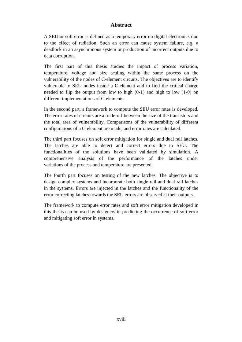
Abstract
A SEU or soft error is defined as a temporary error on digital electronics due
to the effect of radiation. Such an error can cause system failure, e.g. a
deadlock in an asynchronous system or production of incorrect outputs due to
data corruption.
The first part of this thesis studies the impact of process variation,
temperature, voltage and size scaling within the same process on the
vulnerability of the nodes of C-element circuits. The objectives are to identify
vulnerable to SEU nodes inside a C-element and to find the critical charge
needed to flip the output from low to high (0-1) and high to low (1-0) on
different implementations of C-elements.
In the second part, a framework to compute the SEU error rates is developed.
The error rates of circuits are a trade-off between the size of the transistors and
the total area of vulnerability. Comparisons of the vulnerability of different
configurations of a C-element are made, and error rates are calculated.
The third part focuses on soft error mitigation for single and dual rail latches.
The latches are able to detect and correct errors due to SEU. The
functionalities of the solutions have been validated by simulation. A
comprehensive analysis of the performance of the latches under
variations of the process and temperature are presented.
The fourth part focuses on testing of the new latches. The objective is to
design complex systems and incorporate both single rail and dual rail latches
in the systems. Errors are injected in the latches and the functionality of the
error correcting latches towards the SEU errors are observed at their outputs.
The framework to compute error rates and soft error mitigation developed in
this thesis can be used by designers in predicting the occurrence of soft error
and mitigating soft error in systems.
xix
Glossary
CD Completion Detector
DI Delay Insensitive
DIL C-
element
Differential logic and an inverter latch C-element
DRAM Dynamic Random Access Memory
ED Error Detection
EDC Error Detection and Correction
EDCD Error detection and correction for dual rail data
EDCDT Error detection and correction with transient correction for
dual rail
EDD Error detection for dual rail data
FPGA Field Programmable Gate Array
FF Fast NMOS and PMOS
FIT Failure-in Time
FNSP Fast NMOS and slow PMOS
GALS Globally asynchronous locally synchronous
IC Integrated Circuit
LE Logic Element
MUX Multiplexer
QDI Quasi Delay Insensitive
SC C-element Single rail with conventional pull-up pull-down C-element
SEU Single Event Upset
SET Single Event Transient
SI Speed Independent
SIL C-
element
Single rail with feedback C-element

xx
SNFP Slow NMOS fast PMOS
SRAM Static Random Access Memory
SS Slow NMOS and PMOS
SS C-element Single rail symmetric implementation C-element
STG State Transition Graph
TT Typical PMOS and NMOS

xxi
Acknowledgements
I would like to thanks my supervisors Prof Alex Yakovlev and Dr Alex
Bystrov for their guidance and supports throughout my studies. It is not
possible to complete the project without their support
My wife, Lily Saidon and my two kids, Tisham and Ihsan have given their
undivided support and time to me to complete my thesis.

xxii
1
Chapter 1. Introduction
Chapter 1 presents the motivation behind the research, the objectives, a thesis
overview, the thesis’ contributions and publications.
1.1 Motivation
The demand for higher integration density and lower power consumption has
lead to the scaling of transistor and voltage supply. Technology continues to
improve in modern VLSI design with the number of transistors doubled every
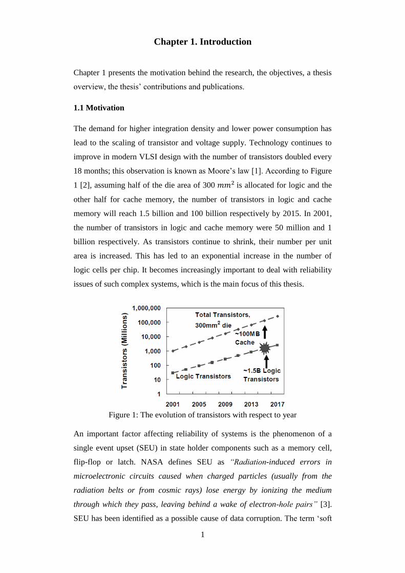
18 months; this observation is known as Moore’s law [1]. According to Figure
1 [2], assuming half of the die area of 300 𝑚𝑚2 is allocated for logic and the
other half for cache memory, the number of transistors in logic and cache
memory will reach 1.5 billion and 100 billion respectively by 2015. In 2001,
the number of transistors in logic and cache memory were 50 million and 1
billion respectively. As transistors continue to shrink, their number per unit
area is increased. This has led to an exponential increase in the number of
logic cells per chip. It becomes increasingly important to deal with reliability
issues of such complex systems, which is the main focus of this thesis.
Figure 1: The evolution of transistors with respect to year
An important factor affecting reliability of systems is the phenomenon of a
single event upset (SEU) in state holder components such as a memory cell,
flip-flop or latch. NASA defines SEU as “Radiation-induced errors in
microelectronic circuits caused when charged particles (usually from the
radiation belts or from cosmic rays) lose energy by ionizing the medium
through which they pass, leaving behind a wake of electron-hole pairs” [3].
SEU has been identified as a possible cause of data corruption. The term ‘soft
2
error’ refers to a temporary error that occurs as a result of particles (alpha
particles from packaging or neutrons from the atmosphere) striking the silicon
structures and causing the state to change from high to low or from low to
high. This electrical effect happens due to the generated electron-hole pairs in
the reverse-biased junction of the victim device.
Nowadays, the dimensions of transistors are very small, as the technology
nodes of 90nm and below (down to 22nm at the time of completion of this
thesis in 2013) became feasible. The drain current and the threshold voltage
are reduced with voltage scaling. As a result, radiation induced soft errors in
the combinational logic are gaining increasing attention and are expected to
become as important as directly induced errors for state elements. The
problem of SEU on transistors has been highlighted by the International
Technology Roadmap for Semiconductors (ITRS), although the problem was
ignored previously until the scaling of transistors had reached deep submicron
technology. In a 2011 report, the ITRS listed SEU as one of the factors
responsible for the decreased reliability of the device.
The severity of SEU toward high density memory devices can be
illustrated on DRAM and SRAM, as they are important elements in an
advanced IC. SRAM is less dense compared with DRAM since it is normally
built from four or six transistors, whereas DRAM is built from a single
transistor and a capacitor.
Data
By
RAM
Size
RAM
Type/Test
Avg FIT
Rate
#Diff
Devs
Range FIT
Rates
Average
Up/bit-
hr
IBM 4M D/A 3500 5* 53-10300 8.9E-13
IBM 1M D/A 3300 2* 2500-4100 3.3E-12
IBM 1M D/F 325 2* 230-420 3.1E-13
Mot 256K S/F 500 3 450-560 2E-12
Mot 1M S/F 2070 2 1330-2800 2.1E-12
Mot 4M S/F 5750 4 4500-8900 1.5E-12
Table 1: Ground level soft error rates measured by RAM
D-DRAM, S-SRAM, F-Field testing, A-Accelerated testing by using proton
beam

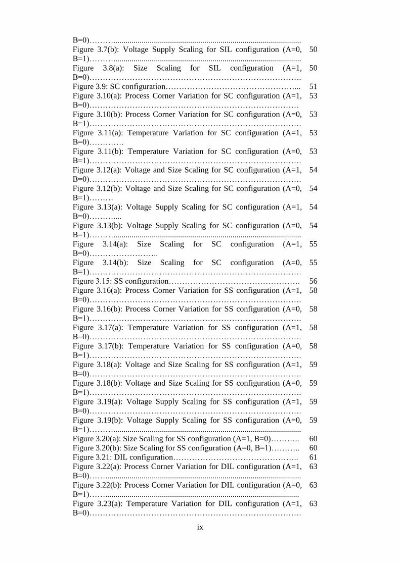
3
From Table 1 [4] it can be observed that DRAM, which is tested using
a proton beam, has an average FIT rate of 3300 for 1M and 3500 for 4M.
Similarly, the average FIT rate for SRAM which has field testing is 2070 for
1M and 5750 for 4M. It is concluded that high density memories have higher
error rates compared with low density memories due to transistor scaling.
Previously, soft errors were a concern for space applications, but now
due to the increase in terrestial radiation, soft error affects everyone. The
problems caused by single event upset can be illustrated by the examples
below in the areas of security and finance:
(a) In the United States alone, 50% of 12 million security cameras sold in
2006 were digital cameras. An average digital camera once a year
experiences an SEU causing its critical failure. So, the the number of
critical failures is approximately 6 million. When a camera is locked due
to SEU, it needs to be reset. This can be costly or in some applications
unacceptable [5].
(b) In a large enterprise such as bank that uses a system of 20,000 processors
one flip-flop experiences one soft error every two days. This is highly
unacceptable to the banking system and stock market as it can lead to
huge losses being inccured by the financial industry. An example of the
adverse effect of SEU on the banking system is when the most
significant digit of the register storing the balance of a bank account flips
from 1 to 0, or vice versa [6].
The demands for lower power consumption have also heightened the need for
asynchronous circuits, since they consume less power compared with
synchronous circuits. However, one of the problems of asynchronous circuits
is that they stay sensitive to SEU continuously for the whole cycle of
operation. For asynchronous circuits, an acknowledgement signal is sent to the
preceding register after the current operation is finished, indicating it is ready
for the next operation. In the event of SEU hitting one of the registers, no
acknowledgement signal is sent and therefore the preceding register does not
assign the next operation to the current computational block. This is in
contrast with synchronous circuits because they become sensitive to SEU only
within a setup-hold window due to the operation being controlled by a global

4
clock. As a result of this, the reliability of synchronous circuits depends
mainly on the upsets in flip-flops, whilst in asynchronous circuits both the
memory elements and the logic gates are important. Compared with other
logics, the C-element is the most important component in asynchronous
circuits and therefore the study of the C-element is vital in order to understand
the reliability of asynchronous circuits towards SEU.
1.2 Objectives
As discussed in Section 1.1, SEU is responsible for temporary data corruption.
This thesis focuses on the factors involved in a state holder experiencing SEU.
The state holder focussed on is the C-element. Different configurations of C-
elements have different vulnerabilities towards SEU. The vulnerability of the
C-element can be compared by calculating the error rate of the individual
nodes and adding the error rate to obtain the total error rate of the individual
circuit.
The second focus of this thesis is on the soft error mitigation in the C-element.
Most existing techniques have many vulnerable nodes especially on C-
element. These vulnerable nodes can be protected against SEU at the expense
of the area of the circuit and the power dissipation. Another factor is the
capability of the circuit, not only that it is able to detect an error but most
importantly it is able to correct the error. This is especially important in
asynchronous circuits because illegal symbols generated from SEU can cause
deadlock. Thus it is worth trading area and power in order to improve circuit
performance against deadlock.
The third focus is on testing the proposed latches against SEU by using
complex logic. This is important to ensure the latches can function correctly
with complex logics. It can also provide the Integrated Circuit (IC) designer
with information on the effectiveness of proposed circuits against SEU.
A set of objectives are summarised below. State-of-the-art software and
equipment has been used, such as Cadence 90-nm technology, Matlab and
Quartus II.
a) To analyse the vulnerability of different configurations of C-elements.
b) To develop a method of calculating the error rate of C-elements.
5
b) To propose error detection and correction of latches built from C-
elements.
c) To test the proposed latches against SEU by using complex logic.
1.3 Thesis Overview
There are eight chapters presented in this thesis.
Chapter 2 presents a literature review, as well as basic concepts of SEU and
asynchronous circuits.
Chapter 3 presents current injection resemble SEU current at the vulnerable
nodes on different configurations of C-elements under four different scenarios:
process corner, temperature, voltage, and size scaling with different inputs
combination of the circuit. The objectives are to identify the vulnerable nodes
due to SEU and to find the critical charges needed to flip the output from low
to high (0-1) and high to low (1-0) on different configurations of C-elements.
Chapter 4 presents an analysis of soft error rate on vulnerable nodes. A new
method is developed to calculate the error rate of the four different C-element
circuits. The total error rates with respect to process corner, temperature,
voltage, and size scaling of the circuits are compared. From the error rate
values, a comparison of vulnerability towards SEU with different
configurations of C-elements can be made with respect to the change of the
four factors above.
Chapter 5 presents an error detection latch (ED) design and error detection
and correction latch (EDC). The functionality of both ED and EDC latches are
demonstrated using Cadence UMC 90nm. The waveforms under fault free
conditions and in the event of an SEU striking the vulnerable nodes are
obtained. The performance of ED and EDC latches are analysed in terms of
propagation delay and switching power.
Chapter 6 presents error detection for a dual rail latch (EDD and error
detection and correction for dual rail latch (EDCD)). The functionality of both
EDD and EDCD latches are demonstrated using Cadence UMC 90nm. The
waveforms under fault free conditions and in the event of SEU striking the
6
vulnerable nodes are obtained. The performance of EDD and EDCD latches
are analysed in terms of propagation delay and switching power. The error
detection and correction with transient error correction latch (EDCDT) is also
proposed in this chapter.
Chapter 7 presents the systems that utilise the proposed EDCD latches. Using
Quartus II, the functionality EDCD latches are demonstrated by using
waveforms under fault free conditions and in the event of SEU hitting the
vulnerable nodes. An asynchronous communication is used to demonstrate the
functionality of EDCD latches. The effect of the system using latches that has
no capablity of detecting and correcting errors is also demonstrated in this
chapter.
Chapter 8 presents conclusions and future work related to the project.
1.4 Thesis Contribution
The contributions of this thesis are as follows:
a) Investigation of the vulnerable node on various C-elements and
obtaining the critical charge on each of the nodes of different
configurations of C-elements.
b) Development of a new technique to calculate the error rate of various
types of C-elements and comparison of each of the C-elements in terms
of vulnerability towards soft error.
c) Design of a single rail error detection latch (ED) and error detection
and correction latch (EDC). The latches are tested with process
variations and temperature changes.
d) Design of a dual rail error detection latch (EDD), dual rail error
detection and correction latch (EDCD), and error detection and
correction with transient correction latch (EDCDT). The latches are
tested with process variations and temperature changes.
e) Implementation of EDCD latch with an asynchronous communication
system.
1.5 Publications
The following papers have been published for publications:
N Julai, A Yakovlev and A Bystrov , Soft Errors Analysis involving C-
Elements Postgraduate Conference Newcastle University 2011

7
N Julai, A Yakovlev and A Bystrov, Soft Errors Analysis involving C-
Elements, UK Electronic Forum, Manchester University 2011
N Julai, A Yakovlev and A Bystrov, Error Detection and Correction of Single
Event Upset (SEU) Tolerant Latch, Postgraduate Conference Newcastle
University 2012
N Julai, A Yakovlev and A Bystrov, Error Detection and Correction of Single
Event Upset (SEU) Tolerant Latch, International On-line Testing Symposium
2012, pp 3-8
8
Chapter 2. Basic Concepts
Chapter 2 presents the literature review and basic concepts of single event
upset (SEU) and asynchronous circuits.
2.1 Radiation Effects in Digital Systems
In section 2.1 radiation is discussed, starting from the sources of radiation, the
effect of radiation on transistors and modelling of current due to radiation. The
focus is on presenting certain ideas and definitions that will help with the
evaluation of calculating the critical charge and the error rate, as discussed
later in chapters 3 and 4.
2.1.1 Sources of Radiation
The particles that can cause error are alpha particles from packaging material
[7] [8], high energy neutrons with energy of more than 1 MeV [9]-[11], and
the interaction of Boron with cosmic ray thermal neutrons [12]-[15]. There are
three main sources of radiation that can cause soft error in electronic devices
[16], as follows:
a) The first source of ionizing radiation is package devices. Package devices
contain certain impurities that are capable of emitting alpha particles.
Alpha particles are produced by a nucleus of unstable isotopes. Alpha
particles are known to have two neutrons and two protons that emit kinetic
energy in the range of 4-9 MeV. There are many different isotopes known
but Uranium and Thorium are the two isotopes that have the highest decay
activities. The decay activities of Uranium and Thorium occur naturally in
the environment. In the terrestrial environment, major sources of alpha
particles are radioactive impurities, such as lead-based isotopes in solder
bumps of flip-chip technology, gold used for bonding wires and lid plating,
aluminium in ceramic packages, lead-frame alloys, and interconnecting
metallization.
b) The second source of ionizing radiation is cosmic rays. At terrestrial
altitude, less than 1% of primary particles from cosmic rays include
muons, pions, protons and neutrons that reach sea level. However, muons
and pions live are brief and therefore do not cause error. Another particle,
protons, are weakened by columbic interaction. The only possibility is that
9
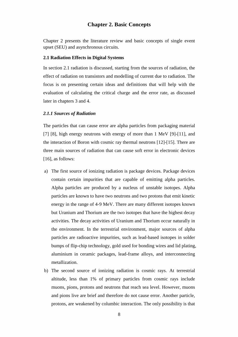
neutrons are the particles that can cause error. The density of neutron
fluxes depends on the altitude (i.e. It is proportional to the altitude). It also
depends on earth magnetic fields, which vary depending on the
geographical location. The neutron energy spectrum that causes SEU is
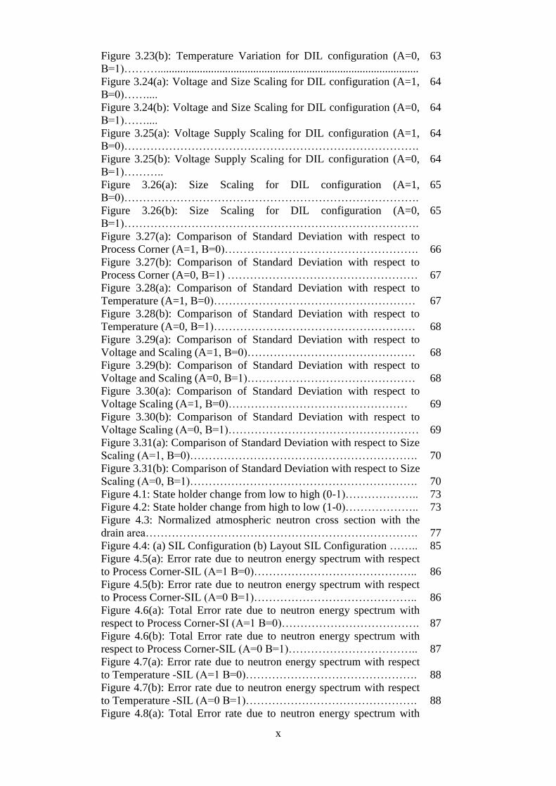
shown in Figure 2.1 [17]. The neutron energy spectrum was obtained
using a neutron beam at Weapon Neutron Research (WNR) in the Los
Angeles Alamos National Laboratory. The neutron beam was used to
obtain a similar energy spectrum as the atmospheric neutron spectrum. At
WNR, neutrons are produced in spallation reactions of 800 MeV protons
incident on a tungsten target which is widely used for SEU testing. From
Figure 2.1 it can be seen that the neutron flux decreased by 10X as the
neutron energy increased by 10X.
Figure 2.1 : Neutron energy spectrum
c) The third significant source that can induce soft error is the interaction of
thermal neutrons and Boron. Boron is used as a p-type dopant implant
species in silicon and used for formation of a BPS dielectric layer. Boron
consists of two isotopes: 𝐵10 (80.1% abundance) and 𝐵11 (19.9%
abundance). However, 𝐵10 is unstable when it interacts with neutrons.
The interaction between 𝐵10 and a neutron results in two particles, 𝐿𝑖7
and alpha particles, being produced. Both newly produced particles are
capable of inducing soft error in electronic devices, as shown in Figure 2.2
[16]. For low energy neutrons (less than 1MeV), the neutrons are not well
defined since neutrons depend on many factors, such as the local
environment, and at this range are more scattered. However, for the

10
purpose of comparison of the spectrum below 1 MeV, the thermal neutron
spectrum [18] is used as shown in Figure 2.3. There are five outdoor
measurements of neutron flux. It can be observed that there are two peaks
of flux, located at 1 MeV to 10−7 MeV.
Figure 2.2: Interaction of Boron and a neutron
Figure 2.3: Neutron spectrum below 1 MeV, including thermal-energy
neutrons
2.1.2 The Effects of Radiation
The drain of an off PMOS and drain of an off NMOS transistor are more
vulnerable toward soft error. Figure 2.4 shows the single event transient (SET)
produced [19]. A neutron from the atmosphere strikes the silicon causing a
collision between the nucleus and the neutron within the substrate. The density
of electron-hole pairs is produced by particles, as shown in Figure 2.4(a). The
carriers are swept to diffusion junction by an electric field and cause the
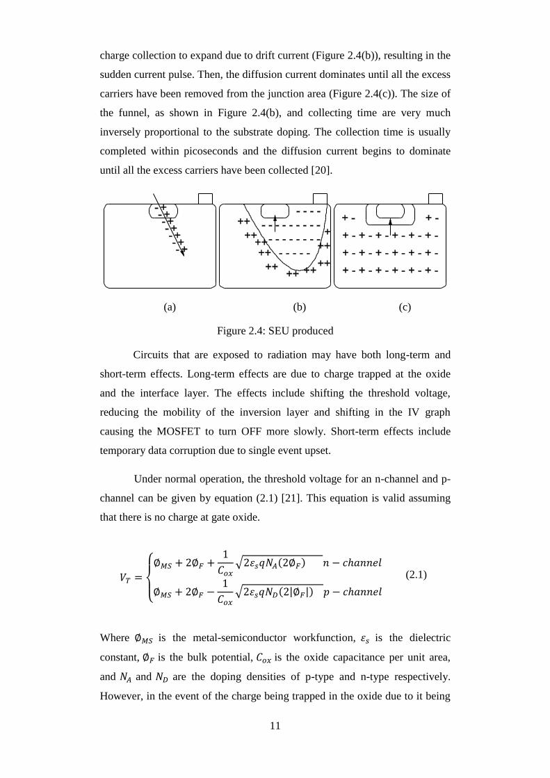
11
charge collection to expand due to drift current (Figure 2.4(b)), resulting in the
sudden current pulse. Then, the diffusion current dominates until all the excess
carriers have been removed from the junction area (Figure 2.4(c)). The size of
the funnel, as shown in Figure 2.4(b), and collecting time are very much
inversely proportional to the substrate doping. The collection time is usually
completed within picoseconds and the diffusion current begins to dominate
until all the excess carriers have been collected [20].
(a) (b) (c)
Figure 2.4: SEU produced
Circuits that are exposed to radiation may have both long-term and
short-term effects. Long-term effects are due to charge trapped at the oxide
and the interface layer. The effects include shifting the threshold voltage,
reducing the mobility of the inversion layer and shifting in the IV graph
causing the MOSFET to turn OFF more slowly. Short-term effects include
temporary data corruption due to single event upset.
Under normal operation, the threshold voltage for an n-channel and p-
channel can be given by equation (2.1) [21]. This equation is valid assuming
that there is no charge at gate oxide.
𝑉𝑇 =
{
∅𝑀𝑆 + 2∅𝐹 +1
𝐶𝑜𝑥√2𝜀𝑠𝑞𝑁𝐴(2∅𝐹) 𝑛 − 𝑐ℎ𝑎𝑛𝑛𝑒𝑙
∅𝑀𝑆 + 2∅𝐹 −1
𝐶𝑜𝑥√2𝜀𝑠𝑞𝑁𝐷(2|∅𝐹|) 𝑝 − 𝑐ℎ𝑎𝑛𝑛𝑒𝑙
(2.1)
Where ∅𝑀𝑆 is the metal-semiconductor workfunction, 𝜀𝑠 is the dielectric
constant, ∅𝐹 is the bulk potential, 𝐶𝑜𝑥 is the oxide capacitance per unit area,
and 𝑁𝐴 and 𝑁𝐷 are the doping densities of p-type and n-type respectively.
However, in the event of the charge being trapped in the oxide due to it being

12
radiation-induced, the change in the threshold voltage is given by equation
(2.2) [21].
∆𝑉𝑇 = −1
𝜀𝑜𝑥∫ 𝑥𝜌0𝑥(𝑥)𝑑𝑥𝑥0𝑥
0
(2.2)
Where 𝑥0𝑥 is the oxide thickness, 𝜀𝑜𝑥 is the dielectric constant, 𝜌0𝑥 is the
volume density charge in the oxide, and 𝑥 is the position in the oxide.
The total change of threshold voltage is given by equation (2.3) [21].
∆𝑉𝑇 = ∆𝑉𝑜𝑡 + ∆𝑉𝑖𝑡 (2.3)
From equation (2.3), the change of threshold voltage due to being radiation
induced consists of two components. The first component is due to the oxide
trapped charge density, 𝑄𝑜𝑡, and is given by equation (2.4) [21].
∆𝑉𝑜𝑡 = −𝑄𝑜𝑡𝐶𝑜𝑥
𝐶𝑜𝑥 =𝜀𝑜𝑥
𝑥𝑜𝑥⁄
(2.4)
The second component is due to the interface trapped charge density, 𝑄𝑖𝑡, and
is given by equation (2.5) [21].
∆𝑉𝑖𝑡 = −𝑄𝑖𝑡𝐶𝑜𝑥
𝐶𝑜𝑥 =𝜀𝑜𝑥
𝑥𝑜𝑥⁄
(2.5)
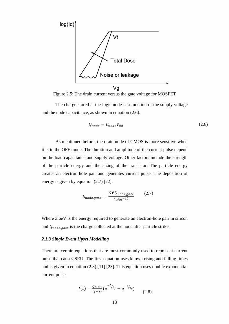
Another effect of being radiation induced is the sub-threshold slope.
The sub-threshold slope represents the time taken for the MOSFET to turn
OFF. The steeper the slope, the quicker the turn OFF time. However, in the
event of radiation, the interface-trap charge increases and the turn OFF time is
longer, causing a leakage current even if there is no voltage applied at the gate
of MOSFET. The drain current versus the gate voltage for MOSFET is shown
in Figure 2.5 [21], illustrating the change in the slope of the drain current in
the event of interface-trap charge due to radiation.
13
Figure 2.5: The drain current versus the gate voltage for MOSFET
The charge stored at the logic node is a function of the supply voltage
and the node capacitance, as shown in equation (2.6).
𝑄𝑛𝑜𝑑𝑒 = 𝐶𝑛𝑜𝑑𝑒𝑉𝑑𝑑 (2.6)
As mentioned before, the drain node of CMOS is more sensitive when
it is in the OFF mode. The duration and amplitude of the current pulse depend
on the load capacitance and supply voltage. Other factors include the strength
of the particle energy and the sizing of the transistor. The particle energy
creates an electron-hole pair and generates current pulse. The deposition of
energy is given by equation (2.7) [22].
𝐸𝑛𝑜𝑑𝑒,𝑔𝑎𝑡𝑒 = 3.6𝑄𝑛𝑜𝑑𝑒,𝑔𝑎𝑡𝑒
1.6𝑒−19
(2.7)
Where 3.6eV is the energy required to generate an electron-hole pair in silicon
and 𝑄𝑛𝑜𝑑𝑒,𝑔𝑎𝑡𝑒 is the charge collected at the node after particle strike.
2.1.3 Single Event Upset Modelling
There are certain equations that are most commonly used to represent current
pulse that causes SEU. The first equation uses known rising and falling times
and is given in equation (2.8) [11] [23]. This equation uses double exponential
current pulse.
𝐼(𝑡) =𝑄𝑡𝑜𝑡𝑎𝑙
𝜏𝑓− 𝜏𝑟(𝑒−𝑡
𝜏𝑓⁄ − 𝑒−𝑡
𝜏𝑟⁄ )
(2.8)
14
Where 𝜏𝑟 and 𝜏𝑓 represent rising and falling time respectively. The author of
[24, 25] suggested that the constant 𝜏𝑟 and 𝜏𝑓 is 50 ps and 164 ps
respectively. 𝑄𝑡𝑜𝑡𝑎𝑙 represents the total collected charge after the current pulse
hits the vulnerable nodes.
The second equation uses single exponential current pulse. Unlike the
first equation that uses rising and falling time, this equation uses process
technology-dependent time constant and is given in equation (2.9).
𝐼(𝑡) =2𝑄𝑡𝑜𝑡𝑎𝑙
𝑇√𝜋√𝑡
𝑇𝑒−𝑡
𝑇⁄
(2.9)
Where 𝑄𝑡𝑜𝑡𝑎𝑙 is the amount of collected charge and T is a process technology-
dependent time constant.
Based on equations (2.8) and (2.9), several publications have been
published to model current pulse in the simplest form. Since the above current
pulse modelling is non-linear, approximation needs to be done to avoid the
complexities of the equations. Based on the literature and previous works on
modelling current pulse, three different shapes are identified: piece-wise linear
function-shaped, triangular-shaped, and trapezoidal-shaped.
The author of [26] modelled the current pulse as a piece-wise linear
function, as shown by Figure 2.6.
Figure 2.6: Piece-wise linear function modelling for SEU
The peak represents funnelling charge collection and the tail represents
decaying charge. The model was injected in 6T SRAM, since it is the most
15
convenient circuit to obtain verification. Results showed that the simulated
data agreed with the experimental data based on 0.25 um technology.
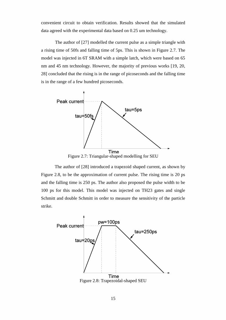
The author of [27] modelled the current pulse as a simple triangle with
a rising time of 50fs and falling time of 5ps. This is shown in Figure 2.7. The
model was injected in 6T SRAM with a simple latch, which were based on 65
nm and 45 nm technology. However, the majority of previous works [19, 20,
28] concluded that the rising is in the range of picoseconds and the falling time
is in the range of a few hundred picoseconds.
Figure 2.7: Triangular-shaped modelling for SEU
The author of [28] introduced a trapezoid shaped current, as shown by
Figure 2.8, to be the approximation of current pulse. The rising time is 20 ps
and the falling time is 250 ps. The author also proposed the pulse width to be
100 ps for this model. This model was injected on TH23 gates and single
Schmitt and double Schmitt in order to measure the sensitivity of the particle
strike.
Figure 2.8: Trapezoidal-shaped SEU

16
2.2 Asynchronous Design
In this section the asynchronous design is discussed, including the advantages
of asynchronous design, the classification of asynchronous design, the C-
element and the implementation. It is not the goal of these sections to cover all
related theories of asynchronous design but rather to focus on certain ideas and
key components that will help the evaluation of asynchronous design
presented in chapters 5 to 7.
2.2.1 Advantages of Asynchronous Design
In digital design there are two types of design: synchronous design and
asynchronous design. In synchronous design, a global clock is one of the main
systems that consumes a lot of power. Power in synchronous design is
consumed by the clock even if there is no data processing taking place.
Asynchronous design that depends on data is clockless and as far as the power
is concerned, asynchronous design does not consume much power compared
with synchronous design, which really makes asynchronus design the
preffered choice for low power consumption. Besides having low power
consumption, there are many advantages of aynchronous design compared
with synchronous design.
(a) Absence of clock skew
Clock skew refers to the arrival time difference of the clock signal
reaching different parts of the system and is one of the main design
challenges in synchronous design. The presence of process variations
may cause adverse effects on clock frequencies.
(b) Better than worst case performance
The worst case scenario needs to be taken into account in synchronous
design to ensure the circuit will not fail under the worst case scenario.
For asynchronous design, the average case performance is the most
likely case due to the data-dependant data flow and functional unit that
shows data-dependant delay.
(c) Automatic adaption to physical properties
Delay depends on many factors, such as process variation, environment
factors (temperature) and voltage supply. In synchronous design, these
factors need to be considered and to ensure the design is reliable, the
17
worst of the above conditions needs to be calculated accordingly.
However, in asynchronous design, since it is depends on the data as a
clock, the above factors are adjusted and hence the designer need not
worry about the functionality of the circuit even under the worst case
scenario.
(e) Reduced electromagnetic interference
A synchronous circuit needs to be very precise in terms of the clock
system and this results in a very narrow spectral band in the clock
frequency. Any interference, for example due to electromagnetic
interference, with the system clock in synchronous design may result in
the circuit functioning slower or even to the extend of failing
completely. This is not the case for asynchronous design as the
activities of the circuit are very much independent from one another.
Therefore, a more distributed noise spectrum which results from
independent activities in asynchronous design makes the circuit more
dependable compared with synchronous design.
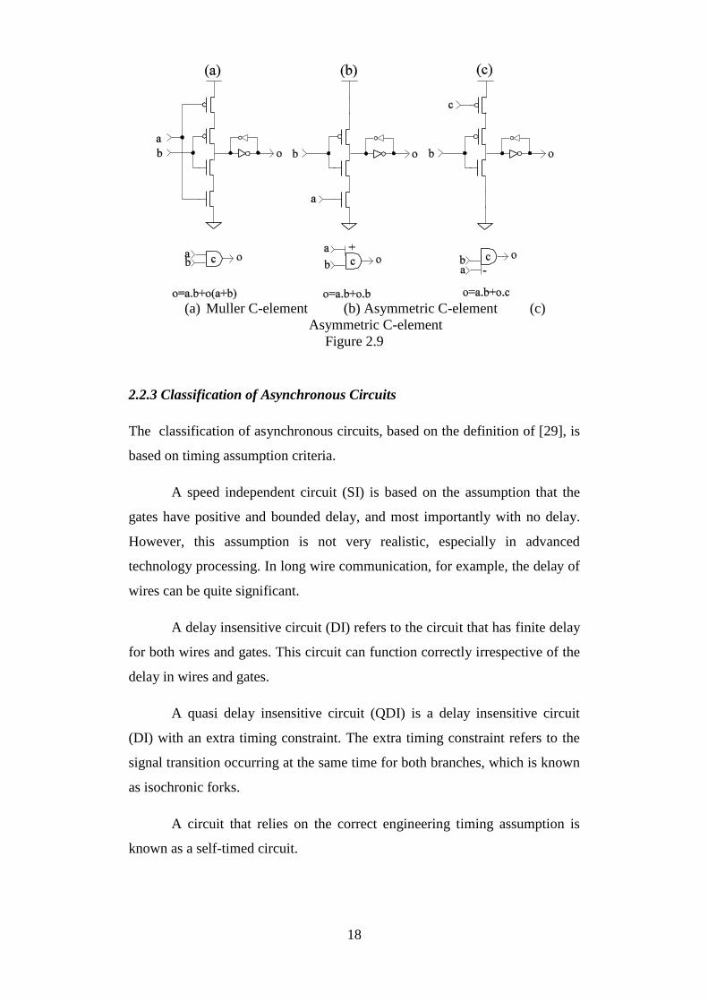
2.2.2 C-Element
As mentioned above, one of the disadvantages of asynchronous circuits is
circuit failure due to deadlock: a state where the system will be disabled
indefinitely until the system has been reset or the error is filtered or corrected
from the system. That means the circuit will be in the waiting state unless
there is feedback or some kind of acknowledgement signal, since it is depends
on the data itself rather than the clock to function. The C-element is one of the
most commonly found circuits in asynchronous circuits, as shown in Figure
2.9(a). The C-element gives logic 0 and 1 if both inputs are 0 and 1
respectively. It maintains the previous value if the inputs are not equal. Figures
2.2.1(b) and 2.2.1(c) also show the asymmetric C-element which is derived
from a Muller C-element. The difference between them is the number of
PMOS and NMOS transistors present in the circuit. In Figure 2.9(b), the
output is 1 only if both inputs are 1. However, if input b is 0, the output is 0,
irrespective of the value of b. Similarly, in Figure 2.9(c), if input b is 0, then
the output is 0, irrespective of the value of c.
18
(a) Muller C-element (b) Asymmetric C-element (c)
Asymmetric C-element
Figure 2.9
2.2.3 Classification of Asynchronous Circuits
The classification of asynchronous circuits, based on the definition of [29], is
based on timing assumption criteria.
A speed independent circuit (SI) is based on the assumption that the
gates have positive and bounded delay, and most importantly with no delay.
However, this assumption is not very realistic, especially in advanced
technology processing. In long wire communication, for example, the delay of
wires can be quite significant.
A delay insensitive circuit (DI) refers to the circuit that has finite delay
for both wires and gates. This circuit can function correctly irrespective of the
delay in wires and gates.
A quasi delay insensitive circuit (QDI) is a delay insensitive circuit
(DI) with an extra timing constraint. The extra timing constraint refers to the
signal transition occurring at the same time for both branches, which is known
as isochronic forks.
A circuit that relies on the correct engineering timing assumption is
known as a self-timed circuit.
19
2.2.4 Asynchronous Circuit Implementation
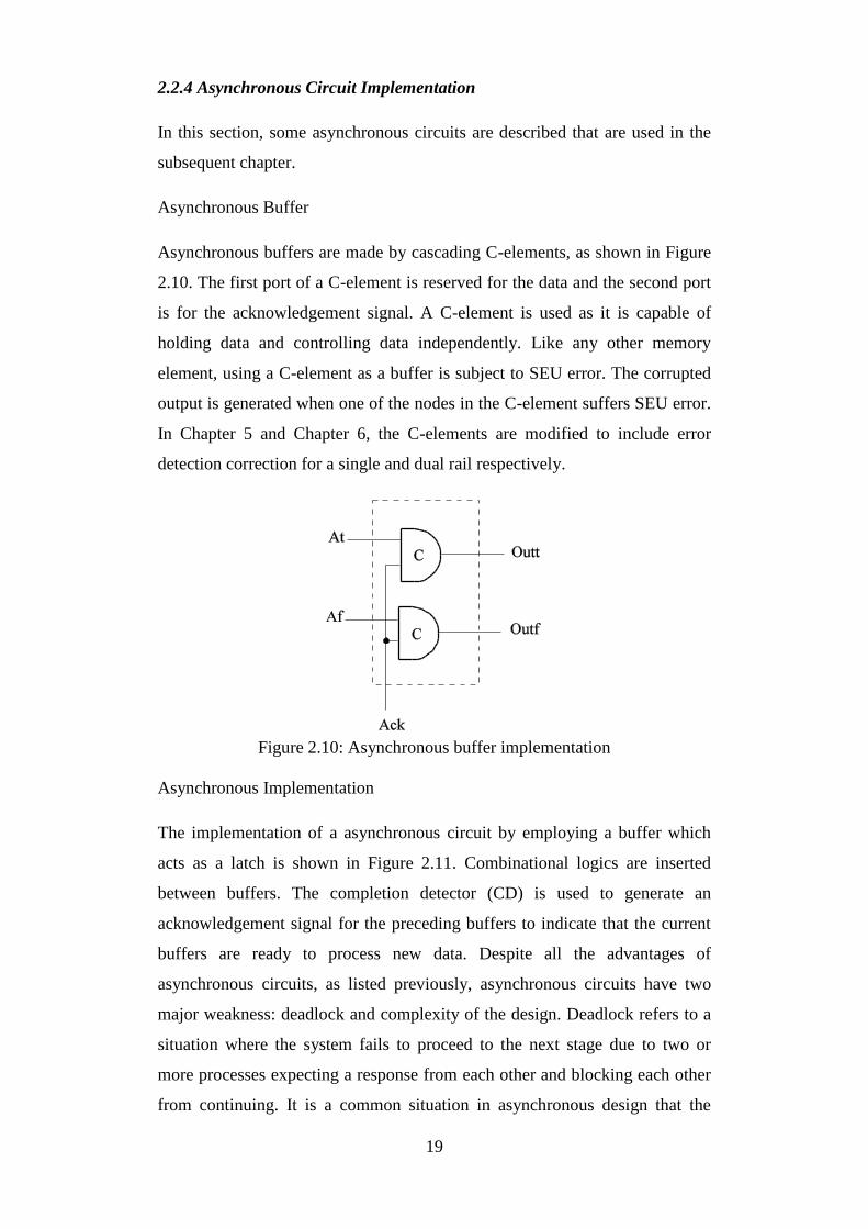
In this section, some asynchronous circuits are described that are used in the
subsequent chapter.
Asynchronous Buffer
Asynchronous buffers are made by cascading C-elements, as shown in Figure
2.10. The first port of a C-element is reserved for the data and the second port
is for the acknowledgement signal. A C-element is used as it is capable of
holding data and controlling data independently. Like any other memory
element, using a C-element as a buffer is subject to SEU error. The corrupted
output is generated when one of the nodes in the C-element suffers SEU error.
In Chapter 5 and Chapter 6, the C-elements are modified to include error
detection correction for a single and dual rail respectively.
Figure 2.10: Asynchronous buffer implementation
Asynchronous Implementation
The implementation of a asynchronous circuit by employing a buffer which
acts as a latch is shown in Figure 2.11. Combinational logics are inserted
between buffers. The completion detector (CD) is used to generate an
acknowledgement signal for the preceding buffers to indicate that the current
buffers are ready to process new data. Despite all the advantages of
asynchronous circuits, as listed previously, asynchronous circuits have two
major weakness: deadlock and complexity of the design. Deadlock refers to a
situation where the system fails to proceed to the next stage due to two or
more processes expecting a response from each other and blocking each other
from continuing. It is a common situation in asynchronous design that the
20
system faces deadlock due to incorrect circuit design, token missmatch and
also arbitration. Single event upset (SEU) can also cause a circuit to have
deadlock due to data corruption. The design of CD is a trivial task but in some
cases it is a complex task since the asynchronous design is data dependant.
The simplest CD is a dual rail CD which is basically an XOR gate. For an m to
n code detector, the CD is a complex circuit and this complex CD adds extra
hardware to the system and the design is made even more complex with the
CD.
Figure 2.11: Asynchronous implementation
MUX
MUX is used to steer multiple inputs to one output by selecting the select line
(Sel) to choose the appropriate inputs, as shown in Figure 2.12. In Chapter 5
and Chapter 6, the proposed error detection and correction latches incorporate
the use of MUX to select the correct value. The first port of MUX is connected
with the main latch and the other port is connected with the shadow latch. In
the event of SEU, the value from the shadow latch is selected to correct the
SEU error.
Figure 2.12: Multiplexer (MUX)
21
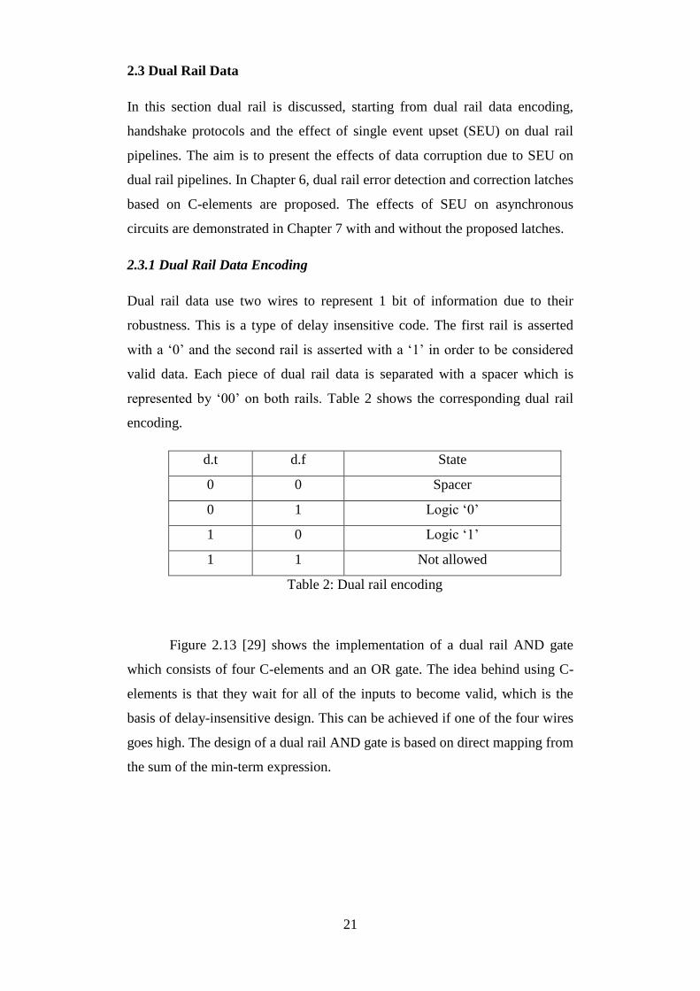
2.3 Dual Rail Data
In this section dual rail is discussed, starting from dual rail data encoding,
handshake protocols and the effect of single event upset (SEU) on dual rail
pipelines. The aim is to present the effects of data corruption due to SEU on
dual rail pipelines. In Chapter 6, dual rail error detection and correction latches
based on C-elements are proposed. The effects of SEU on asynchronous
circuits are demonstrated in Chapter 7 with and without the proposed latches.
2.3.1 Dual Rail Data Encoding
Dual rail data use two wires to represent 1 bit of information due to their
robustness. This is a type of delay insensitive code. The first rail is asserted
with a ‘0’ and the second rail is asserted with a ‘1’ in order to be considered
valid data. Each piece of dual rail data is separated with a spacer which is
represented by ‘00’ on both rails. Table 2 shows the corresponding dual rail
encoding.
d.t d.f State
0 0 Spacer
0 1 Logic ‘0’
1 0 Logic ‘1’
1 1 Not allowed
Table 2: Dual rail encoding
Figure 2.13 [29] shows the implementation of a dual rail AND gate
which consists of four C-elements and an OR gate. The idea behind using C-
elements is that they wait for all of the inputs to become valid, which is the
basis of delay-insensitive design. This can be achieved if one of the four wires
goes high. The design of a dual rail AND gate is based on direct mapping from
the sum of the min-term expression.

22
Figure 2.13: Dual rail AND gate
In an asynchronous circuit, the Muller pipeline forms the basis of the
control system, employing dual rail data. Figure 2.14 [29] shows the Muller
pipeline latch which is constructed mainly of C-elements, inverters and an OR
gate.
Figure 2.14: Muller pipeline latch
The functionality of the Muller pipeline can be described as follows. Suppose
the output, do.f and do.t, holds a spacer. This causes a ‘0’ to propagate to the
inverter and cause acko to be in logic ‘1’. Consequently, in the next stage the
Muller latch is ready to latch data and set acki to logic ‘1’. Similarly, suppose
the output, do.f and do.t, holds valid data. The data is latched and causes acko
to be set to ‘0’. Hence, the previous Muller latch is ready to latch the spacer.
The spacer is latched when acki is changed to logic ‘0’ and when the spacer is
latched, acko is changed to logic ‘1’.
2.3.2 Handshake Protocols
In asynchronous communication, two protocols are commonly used: the 4-
phase dual rail protocol and the 2-phase dual rail protocol. The 4-phase has
disadvantages compared with the 2-phase, such as superfluous return to zero.
As a result, it is more costly in terms of time and money. The 4-phase is
shown in Figure 2.15 [29].
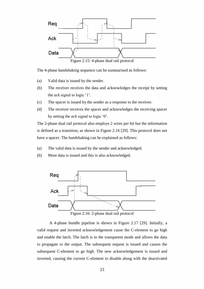
23
Figure 2.15: 4-phase dual rail protocol
The 4-phase handshaking sequence can be summarised as follows:
(a) Valid data is issued by the sender.
(b) The receiver receives the data and acknowledges the receipt by setting
the ack signal to logic ‘1’.
(c) The spacer is issued by the sender as a response to the receiver.
(d) The receiver receives the spacer and acknowledges the receiving spacer
by setting the ack signal to logic ‘0’.
The 2-phase dual rail protocol also employs 2 wires per bit but the information
is defined as a transition, as shown in Figure 2.16 [29]. This protocol does not
have a spacer. The handshaking can be explained as follows:
(a) The valid data is issued by the sender and acknowledged.
(b) More data is issued and this is also acknowledged.
Figure 2.16: 2-phase dual rail protocol
A 4-phase bundle pipeline is shown in Figure 2.17 [29]. Initially, a
valid request and inverted acknowledgement cause the C-element to go high
and enable the latch. The latch is in the transparent mode and allows the data
to propagate to the output. The subsequent request is issued and causes the
subsequent C-element to go high. The new acknowledgement is issued and
inverted, causing the current C-element to disable along with the deactivated

24
signal. This causes the latch to go into the reset mode. When it is in the reset
mode, a new request is issued to the subsequent C-element. This causes the
current C-element in the transparent mode and the process is repeated in this
manner. This process allows valid data to propagate followed by a null.
Figure 2.17: 4-phase bundle pipeline
Figure 2.18 [29] illustrates a 2-phase bundle pipeline without a
processing block which uses 2-phase transition to interpret the control signal.
Basically, there are two control signals, Capture (C) and Pass (P). Assuming
initially the latch is in transparent mode, which allows the input to propagate
to the output; in this instance, the C is equal to P. When there is a valid request
signal, it causes the output of the C-element and consequently the C is flipped.
In this instance C is not equal to P, resulting in the latches to hold their values.
When there is a valid acknowledgement signal the C is equal to P, causing the
latch to be in the transparent mode.
Figure 2.18: 2-phase bundle pipeline
Figure 2.19(a) [30] shows a proposed 2-phase pipeline by Montek
without a processing block known as “Mousetrap”. The working principle of
Mousetrap can be summarised as follows. Assuming data and request signal

25
propagate to the stage, the acknowledgement signal at stage N is sent to the
preceding stage (N-1) and at the same time the stage N pipeline is deactivated
via the XNOR gate. The data and the request signals are then propagated to
stage N+1. The acknowledgement signal (ack(N+1)) is sent to the N-stage and
in this instance enables the stage N pipeline. The delay is inserted, as shown in
Figure 2.19(b) [29], and used to compensate the delay in the processing block.
The Mousetrap function is under the assumption that the request signal is fast
enough to disable the pipeline.
Figure 2.19: 2-phase pipeline Mousetrap
2.3.3 Effects of SEU on Dual Rail Data
Soft error in dual rail encoding can cause data corruption in three different
ways:
a) Data generation - During the reset phase (‘00’), soft error can generate
valid dual rail data, either ‘01’ or ‘10’. This type of error is caused by a
single SEU on a memory circuit. As a result, the CD circuit recognises
this as new data instead of a spacer. Soft error can also cause 1-1 error.
This occurs when valid dual rail data is corrupted by SEU, causing the
data to temporarily change the state from 0 to 1.
b) Data vanishing - Soft error can cause data to temporarily change the
state from 1 to 0. This is known as 0-0 error. The system recognises
this type of error as spacer generation causing the data to disappear. As

26
for data generation error, this type of error is also due to single SEU on
a memory element.
c) Data modification – This error is caused when valid dual rail data
change from ‘10’ to ‘01’. Unlike the case of data generation and data
vanishing, which is caused by single error, this type of error is obtained
by injecting two currents simultaneously in a memory element.
The first case is the circuit function correctly or circuit ignores the
glitch as described by author in [31]. Figure 2.20 shows a one-bit dual rail
under fault free conditions. At time 1, a valid ‘01’ data propagates to the left
channel at time 2. The CD detects the presence of valid data and sends the
acknowledgement signal at time 3. The valid data continues to propagate to
the right channel at time 4 and 5. Upon receiving valid data, the second CD
sends an acknowledgement signal at time 6 and resets the left channel. The
right channel is also reset after time 7, 8 and 9.
Figure 2.20: Fault free 1-bit dual rail
Figure 2.21 illustrates deadlock in the event of SEU on a pipeline due to data
generation. Data generation refers to the generating of new and valid dual rail
data from spacer(null) due to SEU changing the output from 0 to 1. This has
been illustrated by author in [31] as a symbol-loss due to race-through where
the spacing between successive symbols is lost. At time 1, the null propagates
to the left channel and SEU hits one of the C-elements, causing the output of
the C-element to change from 0-1 at time 2. This causes the CD signal to go
high at time 3, as the data is valid data. The data is valid as a result of SEU
being ready to propagate to the right channel at time 4 and 5. The CD signal
recognises it as valid data at time 7 and sends an acknowledgement signal to
the left channel. This causes the left channel to reset and block valid data from
propagating to the left channel. Null appears at time 9 upon receiving requests
at time 8 at the right channel.
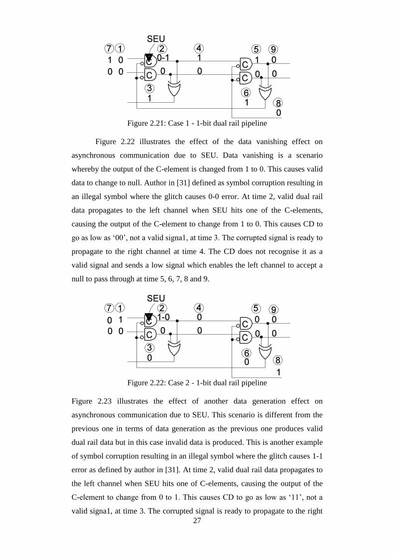
27
Figure 2.21: Case 1 - 1-bit dual rail pipeline
Figure 2.22 illustrates the effect of the data vanishing effect on
asynchronous communication due to SEU. Data vanishing is a scenario
whereby the output of the C-element is changed from 1 to 0. This causes valid
data to change to null. Author in [31] defined as symbol corruption resulting in
an illegal symbol where the glitch causes 0-0 error. At time 2, valid dual rail
data propagates to the left channel when SEU hits one of the C-elements,
causing the output of the C-element to change from 1 to 0. This causes CD to
go as low as ‘00’, not a valid signa1, at time 3. The corrupted signal is ready to
propagate to the right channel at time 4. The CD does not recognise it as a
valid signal and sends a low signal which enables the left channel to accept a
null to pass through at time 5, 6, 7, 8 and 9.
Figure 2.22: Case 2 - 1-bit dual rail pipeline
Figure 2.23 illustrates the effect of another data generation effect on
asynchronous communication due to SEU. This scenario is different from the
previous one in terms of data generation as the previous one produces valid
dual rail data but in this case invalid data is produced. This is another example
of symbol corruption resulting in an illegal symbol where the glitch causes 1-1
error as defined by author in [31]. At time 2, valid dual rail data propagates to
the left channel when SEU hits one of C-elements, causing the output of the
C-element to change from 0 to 1. This causes CD to go as low as ‘11’, not a
valid signa1, at time 3. The corrupted signal is ready to propagate to the right
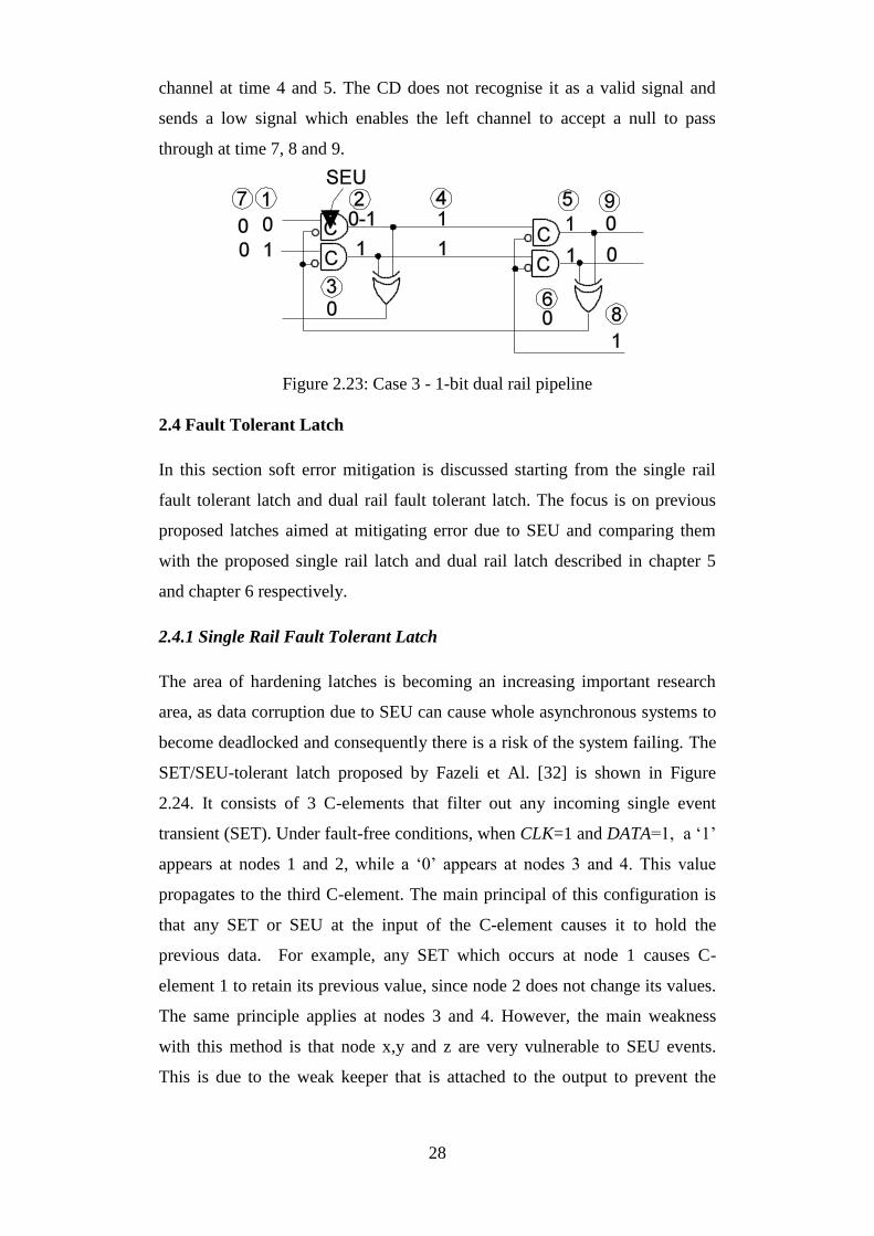
28
channel at time 4 and 5. The CD does not recognise it as a valid signal and
sends a low signal which enables the left channel to accept a null to pass
through at time 7, 8 and 9.
Figure 2.23: Case 3 - 1-bit dual rail pipeline
2.4 Fault Tolerant Latch
In this section soft error mitigation is discussed starting from the single rail
fault tolerant latch and dual rail fault tolerant latch. The focus is on previous
proposed latches aimed at mitigating error due to SEU and comparing them
with the proposed single rail latch and dual rail latch described in chapter 5
and chapter 6 respectively.
2.4.1 Single Rail Fault Tolerant Latch
The area of hardening latches is becoming an increasing important research
area, as data corruption due to SEU can cause whole asynchronous systems to
become deadlocked and consequently there is a risk of the system failing. The
SET/SEU-tolerant latch proposed by Fazeli et Al. [32] is shown in Figure
2.24. It consists of 3 C-elements that filter out any incoming single event
transient (SET). Under fault-free conditions, when CLK=1 and DATA=1, a ‘1’
appears at nodes 1 and 2, while a ‘0’ appears at nodes 3 and 4. This value
propagates to the third C-element. The main principal of this configuration is
that any SET or SEU at the input of the C-element causes it to hold the
previous data. For example, any SET which occurs at node 1 causes C-
element 1 to retain its previous value, since node 2 does not change its values.
The same principle applies at nodes 3 and 4. However, the main weakness
with this method is that node x,y and z are very vulnerable to SEU events.
This is due to the weak keeper that is attached to the output to prevent the

29
output node from entering a high impedance state. It can also be noted that
node x and node y are also vulnerable to SEU.
Figure 2.24: FERST
Omana et Al. [33] proposed the hardened latches shown in Figure 2.25
and Figure 2.26. When CLK=1, the input propagates to the output. At the
output, Out, the resulting signal is fed back to the inputs via two inverters.
This causes either pair of PMOS and NMOS transistors to conduct and
reinforce the output values. As discussed in section 2.1.2, the drain of an off
PMOS and drain of an off NMOS transistor are more vulnerable toward soft
error. Therefore depending on the output, either node x and node y are very
vulnerable to error. There is also a problem with this configuration when a
particle hit occurs at node z. This causes the output to change the state
momentarily to ‘0’ and this value is propagated to both inputs, causing a pair
of NMOS devices to conduct. However, the input to output delay for this
configuration is very small. Another problem with the circuit shown in Figure
2.25 is the electrical contention between the input and the output. In order to
solve the problem, an improved version of SIN-HR, as shown in Figure 2.26,
has been designed to avoid electrical contention between the input and output.
However, the vulnerability to SEU events remains at node x, y and z.
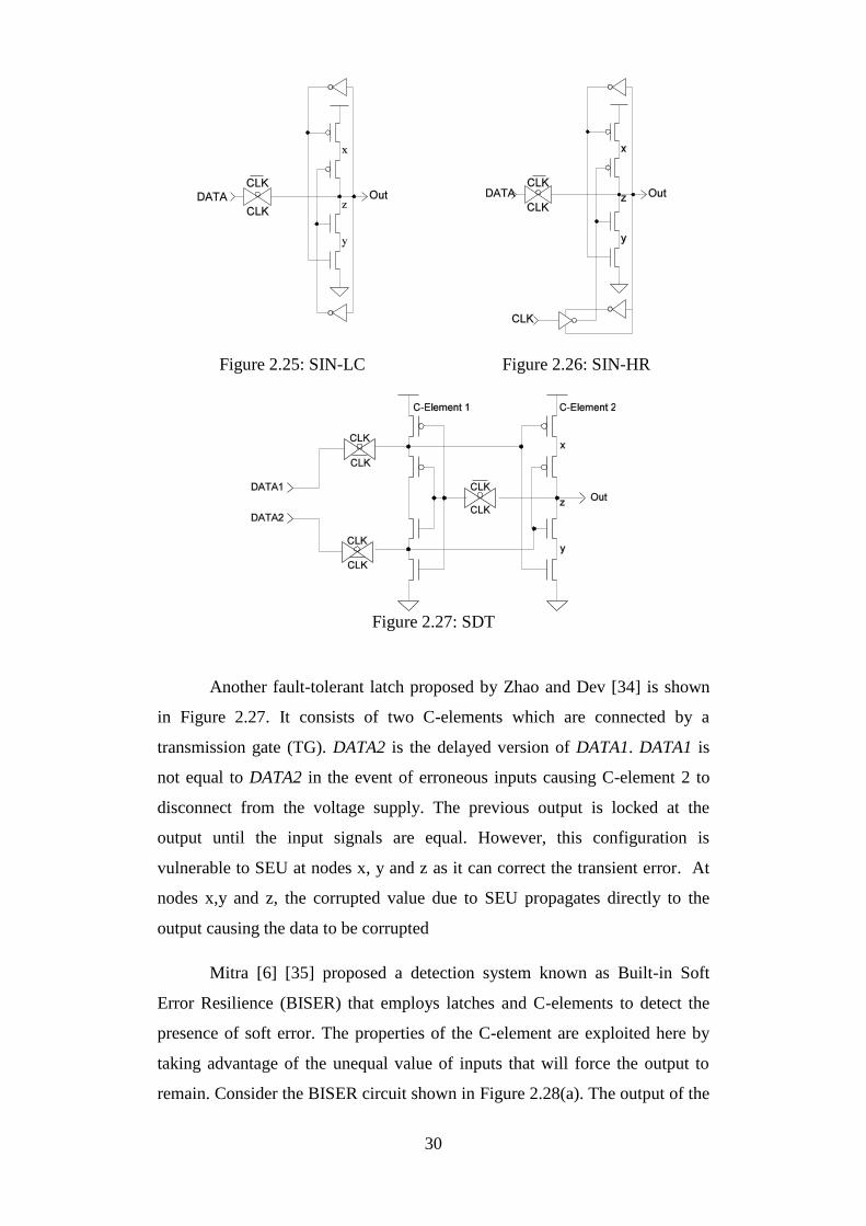
30
Figure 2.25: SIN-LC Figure 2.26: SIN-HR
Figure 2.27: SDT
Another fault-tolerant latch proposed by Zhao and Dev [34] is shown
in Figure 2.27. It consists of two C-elements which are connected by a
transmission gate (TG). DATA2 is the delayed version of DATA1. DATA1 is
not equal to DATA2 in the event of erroneous inputs causing C-element 2 to
disconnect from the voltage supply. The previous output is locked at the
output until the input signals are equal. However, this configuration is
vulnerable to SEU at nodes x, y and z as it can correct the transient error. At
nodes x,y and z, the corrupted value due to SEU propagates directly to the
output causing the data to be corrupted
Mitra [6] [35] proposed a detection system known as Built-in Soft
Error Resilience (BISER) that employs latches and C-elements to detect the
presence of soft error. The properties of the C-element are exploited here by
taking advantage of the unequal value of inputs that will force the output to
remain. Consider the BISER circuit shown in Figure 2.28(a). The output of the

31
combinational logic feeds two latches when CLK =1. The outputs of the
latches, A and B, are compared by the C-element and it propagates if the
values are equal. Suppose a soft error strikes and the values of A and B are not
equal; this forces the old value to be kept by the keeper and hence the error
does not propagate to the output. Two methods as an extension of BISER have
been proposed: soft error logic using duplication and soft error logic using
time shift. By using duplication (Figure 2.28(b)), the combinational logics are
duplicated. The outputs of these duplications are fed into the C-element and
compared using the same techniques as above. The second method (Figure
2.28(c)) exploits the properties of the soft error and places a delay element into
the second input of the C-element. If a soft error strikes, one of the inputs into
the C-element is delayed and compared by the C-element. Therefore, the
presence of soft error can be detected. There are weaknesses with BISER
techniques as a latch. The first problem is suppose SEU strike at the output of
D latches and the outputs are compared by C-element. The error is not
corrected and C-element uses the old values if the inputs is not equal. The
second problem is the use of D-latch which is built from four NAND gates and
one inverter. All of BISER techniques use two D-latch and overhead power
and area increased compared with other proposed latch. The overhead power
and area is very significant with BISER with duplication. In the event of the
inputs of C-element is not equal, nodes x,y and z is vulnerable to soft error and
these nodes are not protected. This error can easily propagates to the outputs
of C-element.
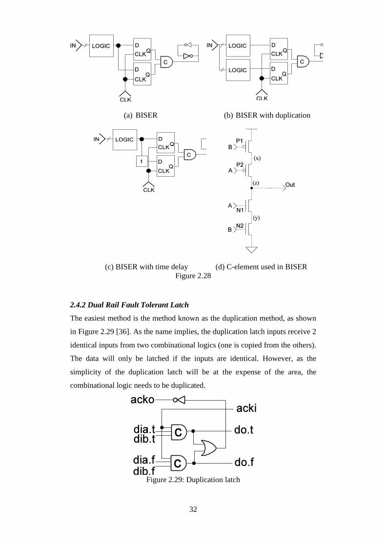
32
(a) BISER (b) BISER with duplication
(c) BISER with time delay (d) C-element used in BISER Figure 2.28
2.4.2 Dual Rail Fault Tolerant Latch
The easiest method is the method known as the duplication method, as shown
in Figure 2.29 [36]. As the name implies, the duplication latch inputs receive 2
identical inputs from two combinational logics (one is copied from the others).
The data will only be latched if the inputs are identical. However, as the
simplicity of the duplication latch will be at the expense of the area, the
combinational logic needs to be duplicated.
Figure 2.29: Duplication latch

33
Monet [37] presented the idea of the rail synchronization latch, as shown
in Figure 2.30, which filters the transient faults or, in the case of undetectable
faults, an appropriate signal (“11”) will be issued. Four possible transient
faults have been proposed by Monet:
a) The fault is stopped by logic gates
b) The fault is not memorized
c) The fault is memorized the circuit operation is not affected
d) The fault is memorized and circuit may fail to function
Basically, the circuit’s computation and memory have two synchronizers, a
pair of D(2) and a pair of Ack(1). If there is a transient fault in the C-element
there will be two possible cases of data, either case c or case d. Case d will be
memorized and compared at the output. The invalid code of “11” will appear
at the output, by assuming valid data has propagated through before the faulty
data is acknowledged.
Figure 2.30: Rail synchronization latch
Gardiner et al. [36] proposed a C-element-based latch that has the
capability of correcting transient error. The proposed latches use four C-
elements to latch dual rail data, controller and logic gates to detect spacer,
error and data. The approach is modified to include error correction for both
transient error and SEU error, in the event of SEU striking the vulnerable node
in the C-element.
The three techniques on dual rail fault tolerant latch have one common
problem which is the use of unprotected C-element expose the latches to SEU
error. There are three vulnerable nodes on two-input C-element and hence the
output data might get corrupted due to SEU.

34
2.5 Factors Affecting CMOS Performance
In this section two factors affecting CMOS performance are discussed. The
aim is to present how the voltage supply, process variation and temperatures
affect the reliability of transistors towards SEU, as described in chapters 3, 4,
5 and 6.
2.5.1 Voltage Supply
Due to the transistors scaling, the supply voltage is scaled down. As a result,
the critical charge needed to change the state is also decreased because the
stored charged needed to flip the output is reduced which is according to the
linear formula
𝑄𝑛𝑜𝑑𝑒 = 𝐶𝑛𝑜𝑑𝑒𝑉𝑑𝑑 (2.10)
𝐶𝑛𝑜𝑑𝑒 = node capacitance, 𝑉𝑑𝑑= supply voltage
The scaling down of voltage supply result in the transistors become more
vulnerable to SEU. SEU will happen when the collected charge is equal to the
critical charge deposited at the junction [27].
2.5.2 Process Variation
Designing integrated circuits (IC) has two main challenges, process variations
of CMOS and environment parameters. One of the methods of testing the
functionality of the design due to process variation is by using process corner
variation. Process corner represents the extremes of parameter variation and
the circuit should be able to function correctly under all process corner
variations. Even though it is rare for the IC to have extreme process variation,
under normal circumstances it is very useful for the designer to test the circuit.
Process variation can be classified into two contributing factors:
a) Die to die variation: This type of variation can affect every element in
the combinational logic.
b) Within die variation - This type of variation can cause non-uniformity
between the devices.
35
As the name implies, process corners can be be classified into 5 types: SS
(slow NMOS and PMOS), FF (fast NMOS and PMOS), TT (typical PMOS
and NMOS), SNFP (slow NMOS fast PMOS), and FNSP (fast NMOS and
slow PMOS). SS, FF and TT are known as even corners since both PMOS and
NMOS transistors are evenly affected. This type of process corner does not
disturb the correctness of the logic function as it only affects the speed of the
devices. The other two process corners (SNFP and FNSP) are known as
skewed corners. These process corners can cause great concern to the designer
due to the disparity in both devices. The disparity between PMOS and NMOS
transistors can cause the logic function to fail. Under process corner variation,
the intended circuit may run slower, faster, at higher or lower temperature,
depending on which process corner is applied. Process corners differ in terms
of nominal threshold voltage, lateral difussion, parasitic capacitances,
temperature, and nominal voltage supply.
2.5.3 Temperature Variation
The other factor is temperature. Temperature can affect the transistor’s
reliability by reducing the drain current, making the transistor more vulnerable
to SEU. The drain current of transistors is given by
𝐼𝑑(𝑇) = 𝜇(𝑇)𝑊
𝐿𝑒𝑓𝑓𝑃𝑙(𝑉𝑔𝑠 − 𝑉𝑇(𝑇))
𝛼
2𝑉𝑑𝑠 (2.11)
𝜇 = mobility constant, 𝑃𝑙= constant to specific technology, VT= threshold
voltage, Leff
= effective channel length, 𝛼= velocity saturation index
Two temperature-dependant factors that can affect the drain current which are
mobility of carriers and the threshold voltage.
As temperature increases, the mobility of the carriers decreases. In other
words, the temperature increase has a negative impact on mobility. The
relation between mobility and temperature is given by equation (2.12).
𝜇(𝑇) = 𝜇(𝑇0) (𝑇𝑇0⁄ )
−𝑚
(2.12)

36
Where 𝑇0 is room temperature and m is the mobility temperature constant
[38].
The constant m has the typical value of 1.5 and can vary for different
processes [39]. Holes move slower than electrons. By increasing temperature,
the mobility of holes is decreased more than the electron due to the critical
electric field for holes decreasing more than the critical electric field for the
electron [40]. Therefore, it is concluded that the reduction of drain current for
PMOS transistors is more comparable with the reduction in drain current for
NMOS transistors. As a result, the vulnerability of PMOS toward SEU is
reduced more than the vulnerability of NMOS with an increase in temperature.
This is shown in Chapter 3.
The temperature increase is inversely proportional to the voltage
threshold which is due to the Fermi energy level and band gap energy shifts
[41]. The relation between voltage threshold and temperature is given in
equation (2.13) below:
𝑉𝑡ℎ(𝑇) = 𝑉𝑡ℎ(𝑇0) − 𝑘(𝑇 − 𝑇0) (2.13)
Where 𝑇0 is room temperature and k is threshold voltage coefficient. From
equation (2.13) it can be concluded that the threshold voltage decreases
linearly as the temperature increases. The typical value of 𝑘 is 0.8 mV/K[42].
As mentioned before, the drain current is also a function of threshold voltage.
When the gate voltage is higher, any change in the threshold voltage does not
effect the drain current. The change of the carrier mobility and saturation
velocity cause significant change to the drain current. However, when the gate
voltage is lower, the drain current is strongly function of the threshold voltage
and overcomes the effect of mobility and saturation velocity. Hence, it makes
the transistors become less temperature dependant.
2.6 CMOS Power Dissipation
In Chapter 5 and Chapter 6 the proposed error detection and correction for
single rail and dual rail is presented. The performance of the latches is
considered by calculating the power dissipation in the event of no error and an
error being detected. Generally, power dissipation in CMOS is the result of
37
switching (dynamic) power, short circuit power and leakage power, as shown
by equation 2.14
𝑃𝑑𝑖𝑠𝑠𝑖𝑝𝑎𝑡𝑖𝑜𝑛 = 𝑃𝑠𝑤𝑖𝑡𝑐ℎ𝑖𝑛𝑔−𝑝𝑜𝑤𝑒𝑟 + 𝑃𝑠ℎ𝑜𝑟𝑡−𝑐𝑖𝑟𝑐𝑢𝑖𝑡 + 𝑃𝑙𝑒𝑎𝑘𝑎𝑔𝑒 (2.14)
Switching power is defined as the power needed to switch the logic
state from 0 to 1. In other words, this is the power needed to charge up the
capacitor. Energy drawn from the voltage supply is used to charge up the
loading capacitor and also dissipated as heat in the circuits. Switching power
is given by
𝑃𝑠𝑤𝑖𝑡𝑐ℎ𝑖𝑛𝑔−𝑝𝑜𝑤𝑒𝑟 = 𝐶𝐿𝑉𝐷𝐷2 𝑃0→1𝑓𝐶𝐿𝐾 (2.15)
CL= loading capacitor, VDD= voltage supply, fCLK= clock frequency, P01=
activity factor
Short circuit power is consumed when both NMOS and PMOS
transistors are ‘ON’. The duration of short circuit power is when
𝑉𝑇𝑛 < 𝑉𝑖𝑛 < 𝑉𝐷𝐷 − 𝑉𝑇𝑝
Short circuit power is estimated as 𝑃𝑠ℎ𝑜𝑟𝑡−𝑐𝑖𝑟𝑐𝑢𝑖𝑡 =1
12𝑘𝜏𝑓𝐶𝐿𝐾(𝑉𝐷𝐷 − 2𝑉𝑇)
3
(2.16) [43]
k= gain factor of transistor, τ= rising and falling time, VT= threshold voltage
When temperature increases, the short circuit power is increased due to the
decreases of threshold voltage, as shown in equation (2.16). The short circuit
power is more significant at high supply voltage than at lower supply voltage.
The third components of power dissipation is due to the leakage power
is given by
𝑃𝑙𝑒𝑎𝑘𝑎𝑔𝑒 = 𝑉𝐷𝐷𝐼𝑙𝑒𝑎𝑘𝑎𝑔𝑒 (2.17)
Leakage current is the result of three factors, which are the reverse bias diode
leakage, gate induced drain leakage current and gate oxide tunnelling. Leakage
current is increased by increasing temperature. A simulation by [44] shows
that the leakage current rises exponentially with supply voltage at 1000𝐶 and
rises linearly at a temperature of 400𝐶 and below.

38
It is concluded from the above discussion that increasing temperature can
deteriorate the reliability towards SEU and increase the power dissipation of
transistors.
39
Chapter 3. Analysis of Single Event Upset on Different
Configurations of C-Elements
This chapter presents current injection resemble single event upset (SEU)
current at the vulnerable nodes on different configurations of C-elements
under four different scenarios: process corner, temperature, voltage, and size
scaling of the circuit. The objectives are to identify the vulnerable nodes due
to SEU and to find the critical charges needed to flip the output from low to
high (0-1) and high to low (1-0) on different configurations of C-elements.
3.1 Introduction
Advancement in silicon technology has resulted in transistors
becoming smaller which has in turn lowered operating voltage and capacitance
[45]. Therefore, these transistors are more sensitive toward radiation-induced
errors. As the demand for low power applications for digital electronics
devices with high density continues to increase, the radiation effect on such
electronic devices is becoming significant. Even though soft error due to
radiation is not a permanent error, this type of error can cause data to be
corrupted.
In this chapter, the current pulse causing SEU is injected into different
nodes of different C-elements. The amplitude of the current is increased until
the output of the C-element is changed. Different configurations of C-elements
are compared in terms of the charges needed to flip the output from 0-1
change or 1-0 change. The minimum charge needed to cause state change is
known as the critical charge.
3.2 Experiments Setup and Work Flow
The workflow of the analysis is summarized below
Step 1: Modelling the current pulse causing Single Event Upset
A current pulse can be represented as having fast rising time and slow
falling time. The amplitude, rising time and falling time of the current pulse
depend on factors such as the type of particle, the energy of the particle and
the angle of the strike. These factors can add complexities in modelling
current pulse. The model shown in Figure 3.1 is used as a current injection to
compare the critical charges between the nodes and C-elements. The model is
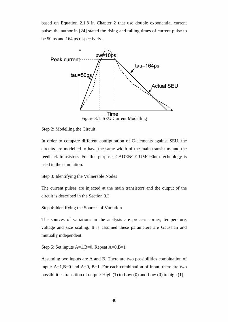
40
based on Equation 2.1.8 in Chapter 2 that use double exponential current
pulse: the author in [24] stated the rising and falling times of current pulse to
be 50 ps and 164 ps respectively.
Figure 3.1: SEU Current Modelling
Step 2: Modelling the Circuit
In order to compare different configuration of C-elements against SEU, the
circuits are modelled to have the same width of the main transistors and the
feedback transistors. For this purpose, CADENCE UMC90nm technology is
used in the simulation.
Step 3: Identifying the Vulnerable Nodes
The current pulses are injected at the main transistors and the output of the
circuit is described in the Section 3.3.
Step 4: Identifying the Sources of Variation
The sources of variations in the analysis are process corner, temperature,
voltage and size scaling. It is assumed these parameters are Gaussian and
mutually independent.
Step 5: Set inputs A=1,B=0. Repeat A=0,B=1
Assuming two inputs are A and B. There are two possibilities combination of
input: A=1,B=0 and A=0, B=1. For each combination of input, there are two
possibilities transition of output: High (1) to Low (0) and Low (0) to high (1).

41
Inputs Outputs
A=1, B=0 0-1
1-0
A=0, B=1 0-1
1-0
Step 6: Varying the Amplitude of SEU Current
As mentioned in step 1, the rising and falling times of the current pulse is
fixed. However, in order to change the area under the curve, the amplitude is
varied until the output is flipped. The simulation is done using circuit analyser
(spectre).
Step 7: Identifying the Amplitude of SEU Current that causes State Change
The amplitude of the current pulse is increased until the output is flipped at
different nodes, different C-elements and different source of variation.
Step 8: Calculating Critical Charge
The critical charge which corresponds to the amplitude of the current pulse
that causes the state to change is obtained at different nodes, different C-
elements and different source of variations.
Step 9: Calculating the Standard Deviation of Critical Charges
Standard deviation of critical charges is calculated to observe the dispersion
value of critical charge when one of the factors mentioned above changes
Step 10: Calculating Error Rates
Error rate is calculated at for each of the nodes of different C-elements. The
total error rate of each C-element is calculated and compared.
Step 11: Calculating Standard Deviation of Errors Rates
Standard deviation of error rate is calculated to observe the dispersion value of
error rate when one of the factors mentioned above changes. Step 9 and step
10 are discussed in Chapter 4.
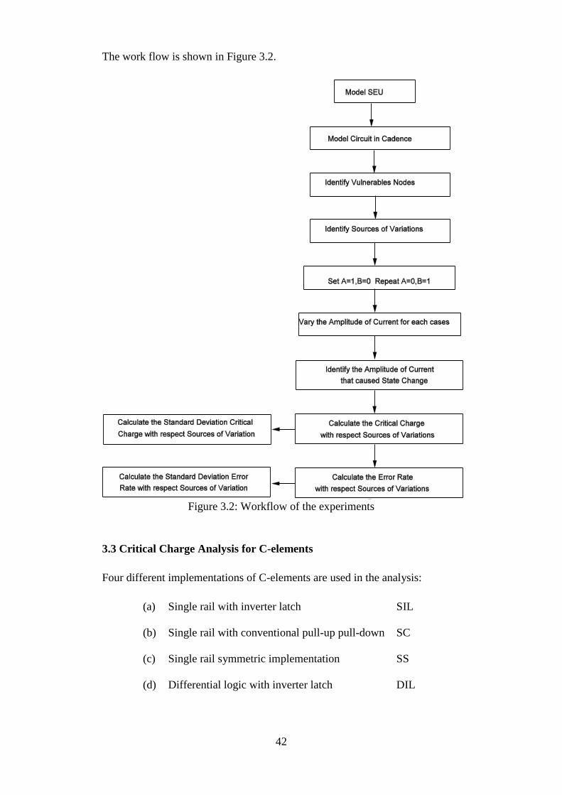
42
The work flow is shown in Figure 3.2.
Figure 3.2: Workflow of the experiments
3.3 Critical Charge Analysis for C-elements
Four different implementations of C-elements are used in the analysis:
(a) Single rail with inverter latch
SIL
(b) Single rail with conventional pull-up pull-down
SC
(c) Single rail symmetric implementation
SS
(d) Differential logic with inverter latch DIL

43
In order to make a fair comparison between different types of C-elements, the
general sizes of the transistors are as follows:
a) The ratio of PMOS and NMOS for the main transistors is 1.125. This
is consistent with Faraday Library for 90 nm technology.
b) The ratio between the main transistor and feedback transistor is 4:1
The analyses are subjected to the following assumptions:
a) The current pulse is assumed to hit the middle of the drain of the Off
PMOS or NMOS transistor. The worst-case scenario is compared with
different implementation of C-elements towards SEU. Thus, the values
might be different to the actual experiments
b) The current pulse is assumed to resemble trapezoidal shapes with fast
rising time and slow falling time and with maximum amplitude.
Current pulse is injected at different nodes for different configurations
of C-elements. The purpose of the experiment is to find the charge needed to
flip the output at the sensitive nodes due to the injected SEU under five
different variables
a) Process corner variation: Five different process corners are varied: TT,
SS, FF, SNFP and FNSP.
b) Temperature variation: Temperature is varied from −40𝑜𝐶 to 100𝑜𝐶
taking only 4 distinct points (−400𝐶, 00𝐶, 270𝐶 and 1000𝐶 ).
c) Voltage supply scaling: Voltage supply is varied from 0.8 V to 1.2 V
(+/-20% of nominal voltage) with 0.1 V step intervals.
d) Size scaling: The widths of all transistors are varied from 50% to 150%
of nominal size with three distinct sizes (50%, 100%, and 150% of
nominal size).
The Latin numerals (i)-(v) are used to denote the sensitive nodes. If the
injected charge is less than the critical charge, it causes no effect to the output
or the pulse is generated and may cause a problem to the combinational logics.
There is further discussion on this in Chapter 4.
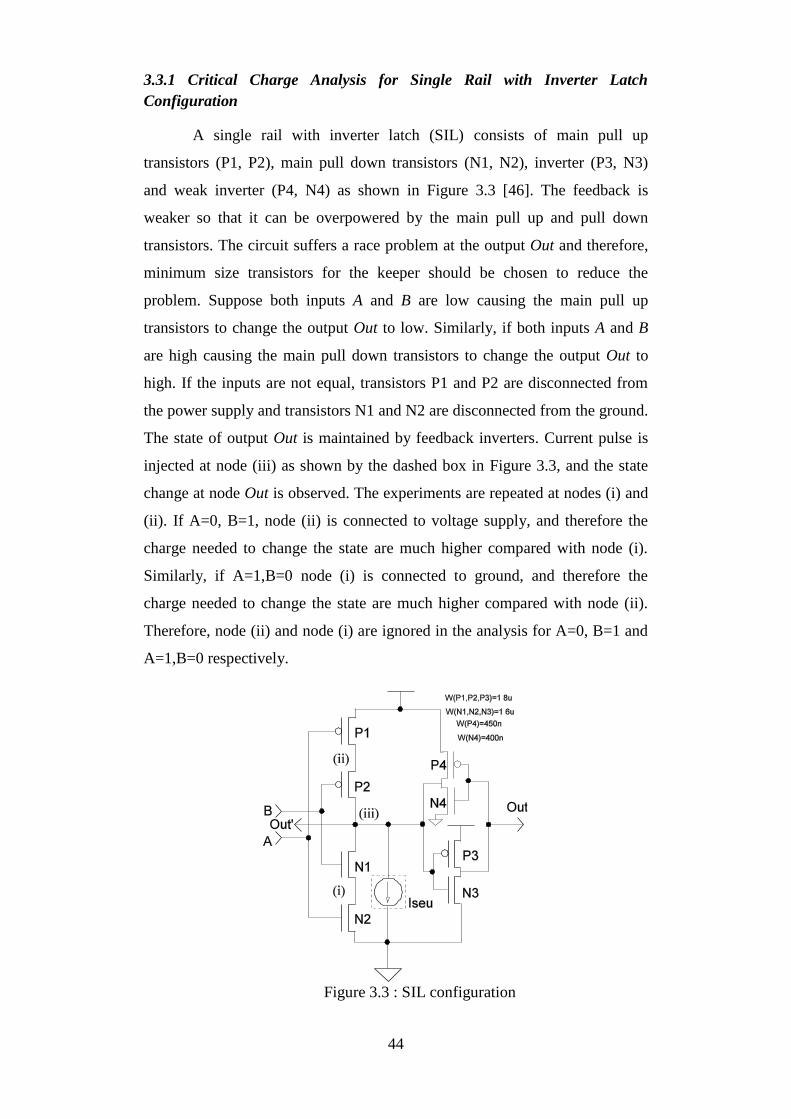
44
3.3.1 Critical Charge Analysis for Single Rail with Inverter Latch
Configuration
A single rail with inverter latch (SIL) consists of main pull up
transistors (P1, P2), main pull down transistors (N1, N2), inverter (P3, N3)
and weak inverter (P4, N4) as shown in Figure 3.3 [46]. The feedback is
weaker so that it can be overpowered by the main pull up and pull down
transistors. The circuit suffers a race problem at the output Out and therefore,
minimum size transistors for the keeper should be chosen to reduce the
problem. Suppose both inputs A and B are low causing the main pull up
transistors to change the output Out to low. Similarly, if both inputs A and B
are high causing the main pull down transistors to change the output Out to
high. If the inputs are not equal, transistors P1 and P2 are disconnected from
the power supply and transistors N1 and N2 are disconnected from the ground.
The state of output Out is maintained by feedback inverters. Current pulse is
injected at node (iii) as shown by the dashed box in Figure 3.3, and the state
change at node Out is observed. The experiments are repeated at nodes (i) and
(ii). If A=0, B=1, node (ii) is connected to voltage supply, and therefore the
charge needed to change the state are much higher compared with node (i).
Similarly, if A=1,B=0 node (i) is connected to ground, and therefore the
charge needed to change the state are much higher compared with node (ii).
Therefore, node (ii) and node (i) are ignored in the analysis for A=0, B=1 and
A=1,B=0 respectively.
Figure 3.3 : SIL configuration
45
Five different process corner variations are performed and the charges
needed to change the state of each process are compared. To observe the
change in critical charge with respect to the process variations, the temperature
is set at 270𝐶 and the voltage supply is set at 1 V. As expected, the SS corner
yields the smallest critical charge and the FF corner yields the highest critical
charge. The highest critical charges of the FF process are due to the larger pull
up and pull down strength of transistors. As a result, the strength of transistors
give better stabilization in the voltage level of the storage node and hence
higher critical charge is needed to flip the output [47]. Figure 3.4(a) shows the
critical charge when inputs A=1, B=0 and Figure 3.4(b) shows the critical
charge when inputs A=0, B=1. The critical charge at nodes (ii), (iii) of 0-1 is
lower than node (ii) and (iii) of 1-0 change when A=1, B=0. Similarly, the
critical charge at nodes (i), (iii) of 0-1 is lower than node (i) and (iii) of 1-0
change when A=0, B=1. The factor variations of critical charges between the
extreme process corner variations are between 1.26X to 1.39X when inputs
A=1, B=0 and 1.28X to 1.47X when inputs A=0, B=1, depending on the
location of the SEU. The critical charges for TT, SNFP and FNSP are
statistically equal since the standard deviation are 0.42f and 0.33f compared
with the standard deviation of SS and FF which are 4f and 2.89f when inputs
A=1, B=0 and inputs A=0, B=1 respectively. Thus, the critical charges for TT,
SNFP and FNSP do not differ much. In the SNFP corner, PMOS transistors
have relatively stronger current compared with NMOS transistors and in the
FNSP corner, NMOS transistors have relatively stronger current compared
with PMOS transistors. However, the stronger PMOS or NMOS transistors
counter balances the weaker NMOS or PMOS transistors and hence produce a
comparable critical charge compared with the TT corner. These findings
suggested that, in general, for the SIL configuration, critical charges are
sensitive to process corner variations in particular the process corners SS and
FF.
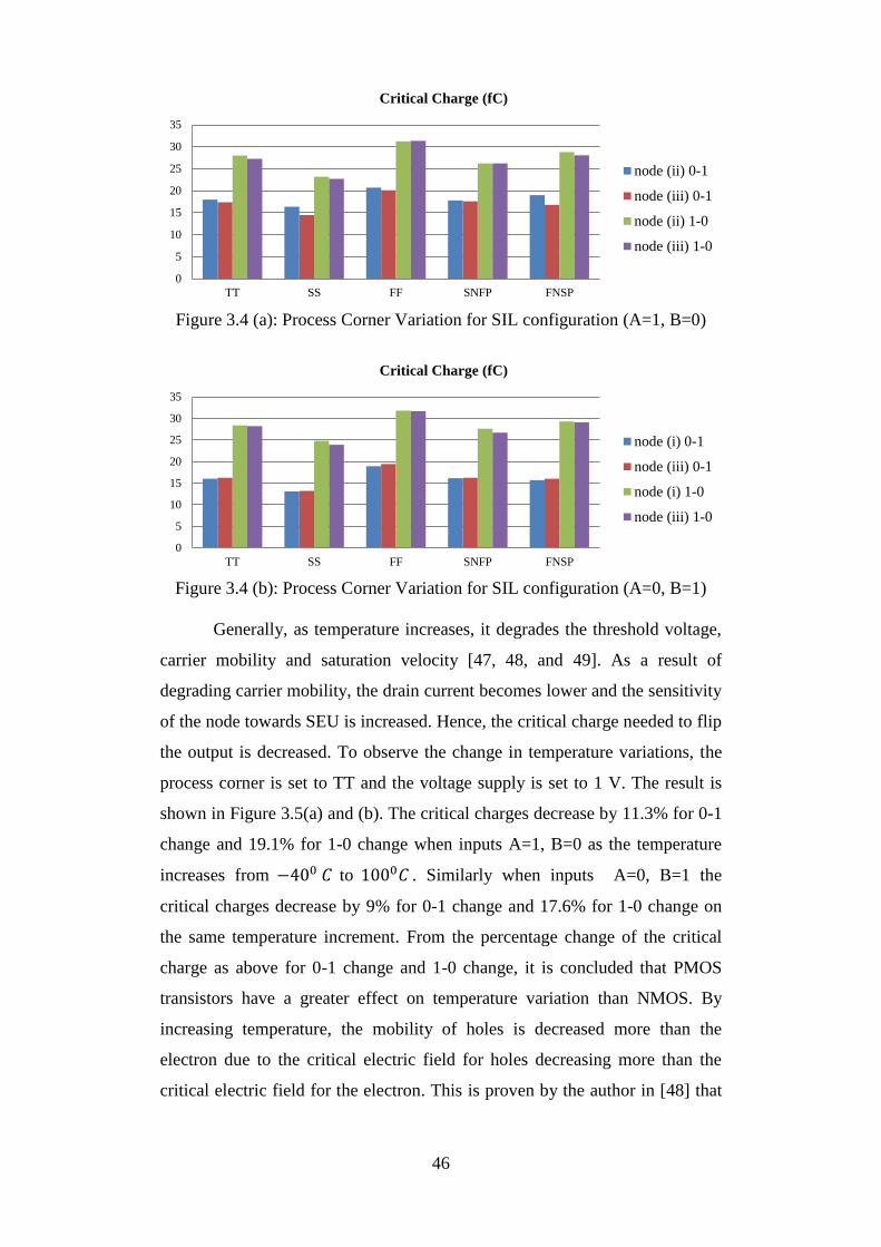
46
Figure 3.4 (a): Process Corner Variation for SIL configuration (A=1, B=0)
Figure 3.4 (b): Process Corner Variation for SIL configuration (A=0, B=1)
Generally, as temperature increases, it degrades the threshold voltage,
carrier mobility and saturation velocity [47, 48, and 49]. As a result of
degrading carrier mobility, the drain current becomes lower and the sensitivity
of the node towards SEU is increased. Hence, the critical charge needed to flip
the output is decreased. To observe the change in temperature variations, the
process corner is set to TT and the voltage supply is set to 1 V. The result is
shown in Figure 3.5(a) and (b). The critical charges decrease by 11.3% for 0-1
change and 19.1% for 1-0 change when inputs A=1, B=0 as the temperature
increases from −400 𝐶 to 1000𝐶 . Similarly when inputs A=0, B=1 the
critical charges decrease by 9% for 0-1 change and 17.6% for 1-0 change on
the same temperature increment. From the percentage change of the critical
charge as above for 0-1 change and 1-0 change, it is concluded that PMOS
transistors have a greater effect on temperature variation than NMOS. By
increasing temperature, the mobility of holes is decreased more than the
electron due to the critical electric field for holes decreasing more than the
critical electric field for the electron. This is proven by the author in [48] that
0
5
10
15
20
25
30
35
TT SS FF SNFP FNSP
Critical Charge (fC)
node (ii) 0-1
node (iii) 0-1
node (ii) 1-0
node (iii) 1-0
0
5
10
15
20
25
30
35
TT SS FF SNFP FNSP
Critical Charge (fC)
node (i) 0-1
node (iii) 0-1
node (i) 1-0
node (iii) 1-0
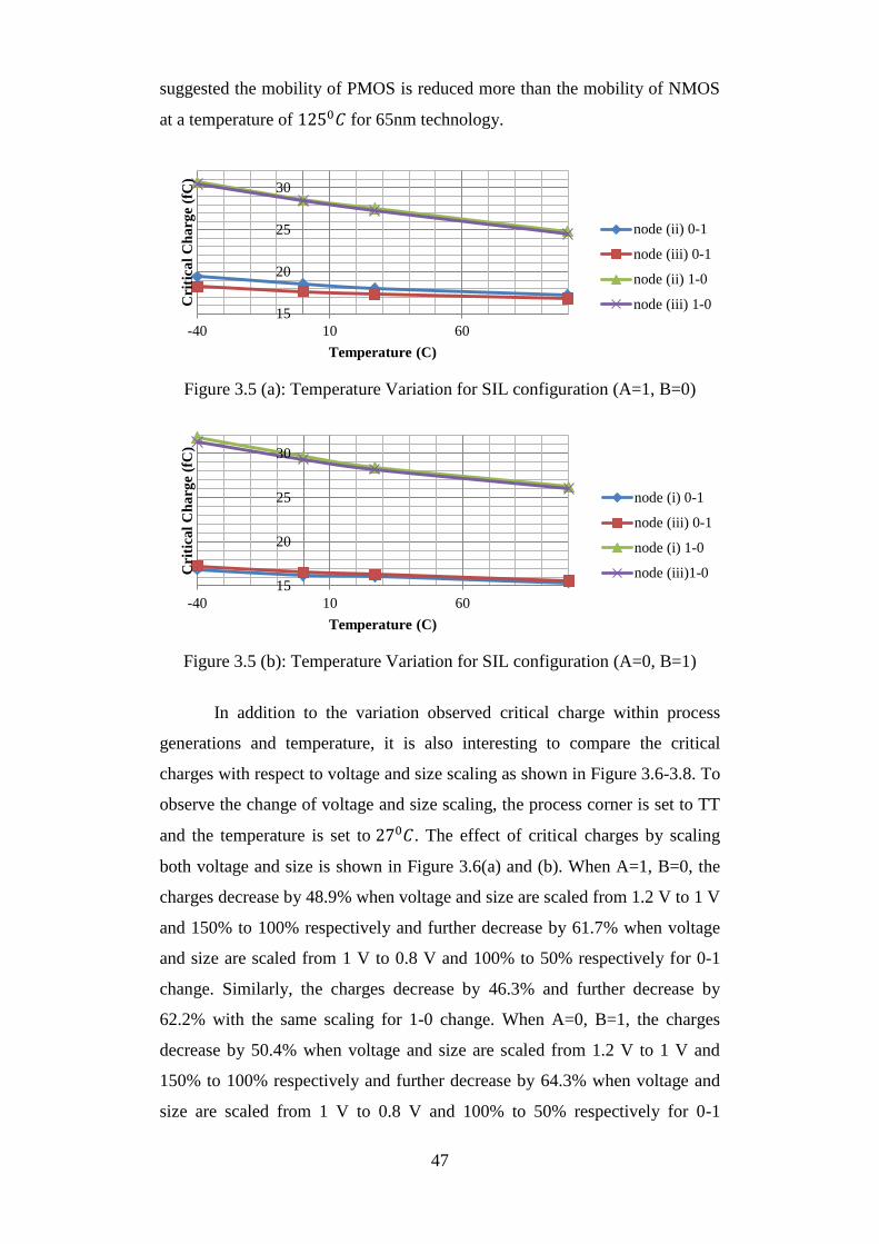
47
suggested the mobility of PMOS is reduced more than the mobility of NMOS
at a temperature of 1250𝐶 for 65nm technology.
Figure 3.5 (a): Temperature Variation for SIL configuration (A=1, B=0)
Figure 3.5 (b): Temperature Variation for SIL configuration (A=0, B=1)
In addition to the variation observed critical charge within process
generations and temperature, it is also interesting to compare the critical
charges with respect to voltage and size scaling as shown in Figure 3.6-3.8. To
observe the change of voltage and size scaling, the process corner is set to TT
and the temperature is set to 270𝐶. The effect of critical charges by scaling
both voltage and size is shown in Figure 3.6(a) and (b). When A=1, B=0, the
charges decrease by 48.9% when voltage and size are scaled from 1.2 V to 1 V
and 150% to 100% respectively and further decrease by 61.7% when voltage
and size are scaled from 1 V to 0.8 V and 100% to 50% respectively for 0-1
change. Similarly, the charges decrease by 46.3% and further decrease by
62.2% with the same scaling for 1-0 change. When A=0, B=1, the charges
decrease by 50.4% when voltage and size are scaled from 1.2 V to 1 V and
150% to 100% respectively and further decrease by 64.3% when voltage and
size are scaled from 1 V to 0.8 V and 100% to 50% respectively for 0-1
15
20
25
30
-40 10 60
Cri
tica
l C
ha
rge
(fC
)
Temperature (C)
node (ii) 0-1
node (iii) 0-1
node (ii) 1-0
node (iii) 1-0
15
20
25
30
-40 10 60
Cri
tica
l C
ha
rge
(fC
)
Temperature (C)
node (i) 0-1
node (iii) 0-1
node (i) 1-0
node (iii)1-0
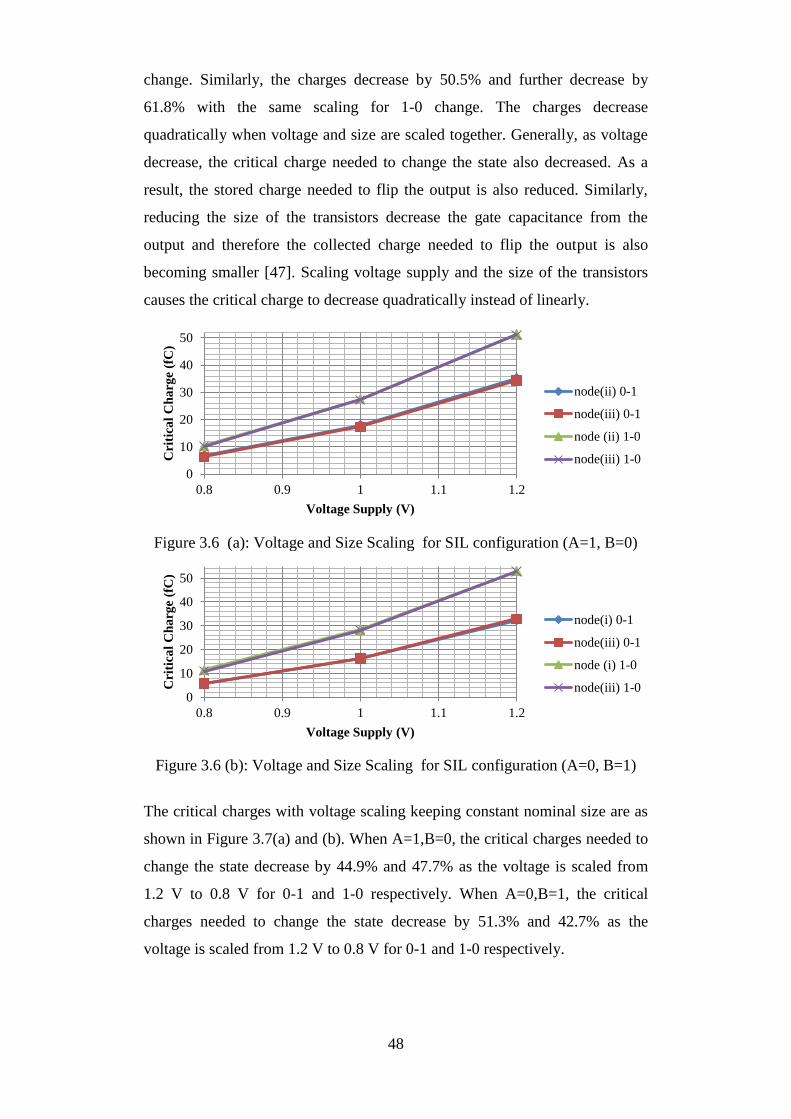
48
change. Similarly, the charges decrease by 50.5% and further decrease by
61.8% with the same scaling for 1-0 change. The charges decrease
quadratically when voltage and size are scaled together. Generally, as voltage
decrease, the critical charge needed to change the state also decreased. As a
result, the stored charge needed to flip the output is also reduced. Similarly,
reducing the size of the transistors decrease the gate capacitance from the
output and therefore the collected charge needed to flip the output is also
becoming smaller [47]. Scaling voltage supply and the size of the transistors
causes the critical charge to decrease quadratically instead of linearly.
Figure 3.6 (a): Voltage and Size Scaling for SIL configuration (A=1, B=0)
Figure 3.6 (b): Voltage and Size Scaling for SIL configuration (A=0, B=1)
The critical charges with voltage scaling keeping constant nominal size are as
shown in Figure 3.7(a) and (b). When A=1,B=0, the critical charges needed to
change the state decrease by 44.9% and 47.7% as the voltage is scaled from
1.2 V to 0.8 V for 0-1 and 1-0 respectively. When A=0,B=1, the critical
charges needed to change the state decrease by 51.3% and 42.7% as the
voltage is scaled from 1.2 V to 0.8 V for 0-1 and 1-0 respectively.
0
10
20
30
40
50
0.8 0.9 1 1.1 1.2
Cri
tica
l C
ha
rge
(fC
)
Voltage Supply (V)
node(ii) 0-1
node(iii) 0-1
node (ii) 1-0
node(iii) 1-0
0
10
20
30
40
50
0.8 0.9 1 1.1 1.2
Cri
tica
l C
ha
rge
(fC
)
Voltage Supply (V)
node(i) 0-1
node(iii) 0-1
node (i) 1-0
node(iii) 1-0
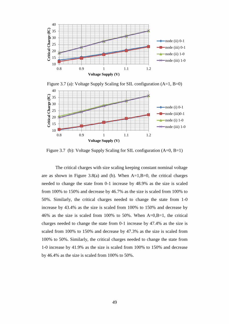
49
Figure 3.7 (a): Voltage Supply Scaling for SIL configuration (A=1, B=0)
Figure 3.7 (b): Voltage Supply Scaling for SIL configuration (A=0, B=1)
The critical charges with size scaling keeping constant nominal voltage
are as shown in Figure 3.8(a) and (b). When A=1,B=0, the critical charges
needed to change the state from 0-1 increase by 48.9% as the size is scaled
from 100% to 150% and decrease by 46.7% as the size is scaled from 100% to
50%. Similarly, the critical charges needed to change the state from 1-0
increase by 43.4% as the size is scaled from 100% to 150% and decrease by
46% as the size is scaled from 100% to 50%. When A=0,B=1, the critical
charges needed to change the state from 0-1 increase by 47.4% as the size is
scaled from 100% to 150% and decrease by 47.3% as the size is scaled from
100% to 50%. Similarly, the critical charges needed to change the state from
1-0 increase by 41.9% as the size is scaled from 100% to 150% and decrease
by 46.4% as the size is scaled from 100% to 50%.
10
15
20
25
30
35
40
0.8 0.9 1 1.1 1.2
Cri
tica
l C
ha
rge
(fC
)
Voltage Supply (V)
node (ii) 0-1
node (iii) 0-1
node (ii) 1-0
node (iii) 1-0
10
15
20
25
30
35
40
0.8 0.9 1 1.1 1.2
Cri
tica
l C
ha
rge
(fC
)
Voltage Supply (V)
node (i) 0-1
node (iii)0-1
node (i) 1-0
node (iii) 1-0
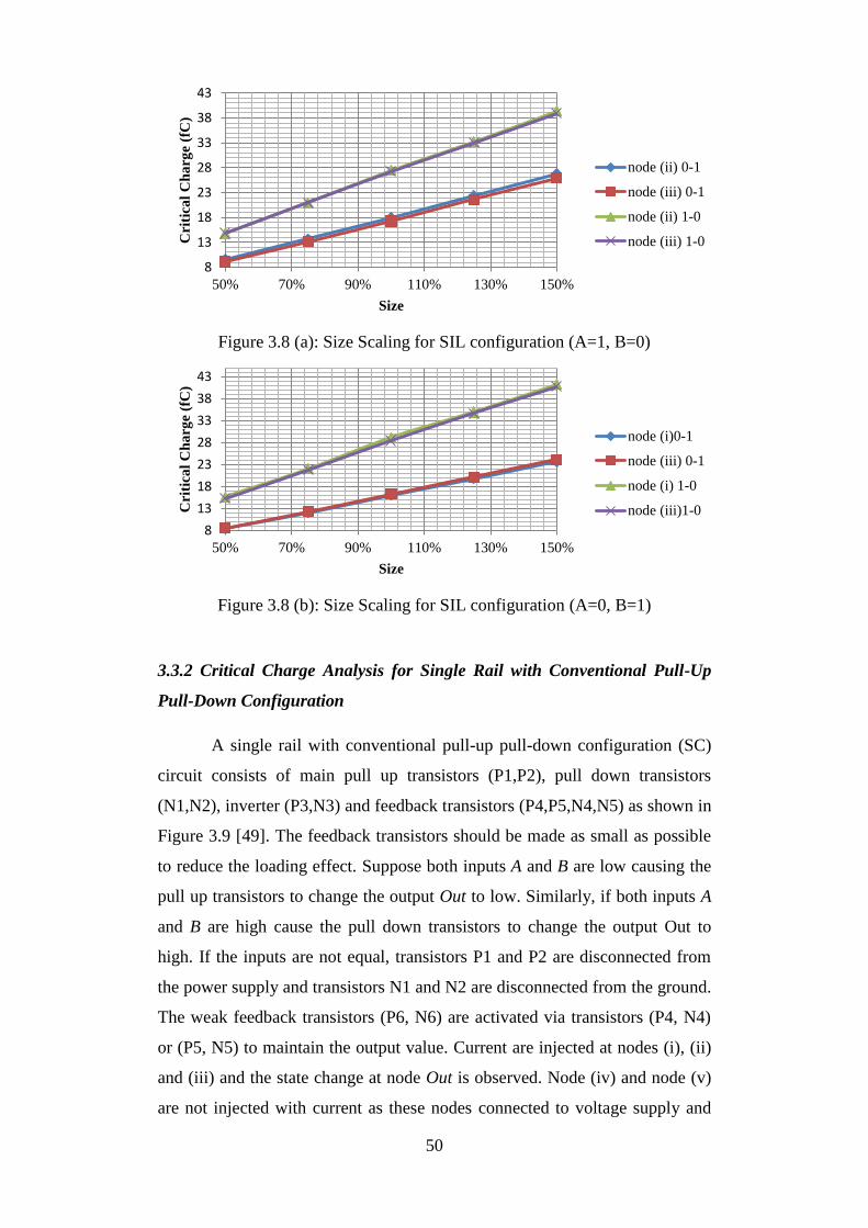
50
Figure 3.8 (a): Size Scaling for SIL configuration (A=1, B=0)
Figure 3.8 (b): Size Scaling for SIL configuration (A=0, B=1)
3.3.2 Critical Charge Analysis for Single Rail with Conventional Pull-Up
Pull-Down Configuration
A single rail with conventional pull-up pull-down configuration (SC)
circuit consists of main pull up transistors (P1,P2), pull down transistors
(N1,N2), inverter (P3,N3) and feedback transistors (P4,P5,N4,N5) as shown in
Figure 3.9 [49]. The feedback transistors should be made as small as possible
to reduce the loading effect. Suppose both inputs A and B are low causing the
pull up transistors to change the output Out to low. Similarly, if both inputs A
and B are high cause the pull down transistors to change the output Out to
high. If the inputs are not equal, transistors P1 and P2 are disconnected from
the power supply and transistors N1 and N2 are disconnected from the ground.
The weak feedback transistors (P6, N6) are activated via transistors (P4, N4)
or (P5, N5) to maintain the output value. Current are injected at nodes (i), (ii)
and (iii) and the state change at node Out is observed. Node (iv) and node (v)
are not injected with current as these nodes connected to voltage supply and
8
13
18
23
28
33
38
43
50% 70% 90% 110% 130% 150%
Cri
tica
l C
ha
rge
(fC
)
Size
node (ii) 0-1
node (iii) 0-1
node (ii) 1-0
node (iii) 1-0
8
13
18
23
28
33
38
43
50% 70% 90% 110% 130% 150%
Cri
tica
l C
ha
rge
(fC
)
Size
node (i)0-1
node (iii) 0-1
node (i) 1-0
node (iii)1-0
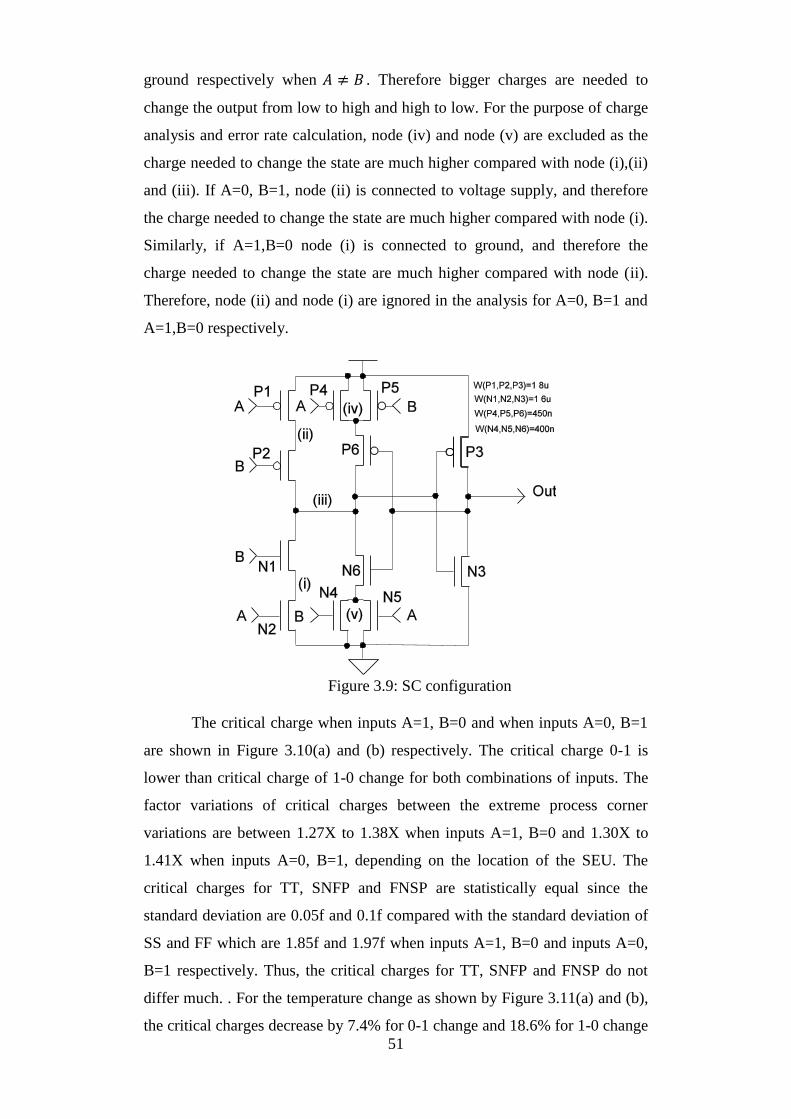
51
ground respectively when 𝐴 ≠ 𝐵 . Therefore bigger charges are needed to
change the output from low to high and high to low. For the purpose of charge
analysis and error rate calculation, node (iv) and node (v) are excluded as the
charge needed to change the state are much higher compared with node (i),(ii)
and (iii). If A=0, B=1, node (ii) is connected to voltage supply, and therefore
the charge needed to change the state are much higher compared with node (i).
Similarly, if A=1,B=0 node (i) is connected to ground, and therefore the
charge needed to change the state are much higher compared with node (ii).
Therefore, node (ii) and node (i) are ignored in the analysis for A=0, B=1 and
A=1,B=0 respectively.
Figure 3.9: SC configuration
The critical charge when inputs A=1, B=0 and when inputs A=0, B=1
are shown in Figure 3.10(a) and (b) respectively. The critical charge 0-1 is
lower than critical charge of 1-0 change for both combinations of inputs. The
factor variations of critical charges between the extreme process corner
variations are between 1.27X to 1.38X when inputs A=1, B=0 and 1.30X to
1.41X when inputs A=0, B=1, depending on the location of the SEU. The
critical charges for TT, SNFP and FNSP are statistically equal since the
standard deviation are 0.05f and 0.1f compared with the standard deviation of
SS and FF which are 1.85f and 1.97f when inputs A=1, B=0 and inputs A=0,
B=1 respectively. Thus, the critical charges for TT, SNFP and FNSP do not
differ much. . For the temperature change as shown by Figure 3.11(a) and (b),
the critical charges decrease by 7.4% for 0-1 change and 18.6% for 1-0 change

52
when inputs A=1, B=0 as the temperature increases from −400 𝐶 to 1000𝐶.
Similarly when inputs A=0, B=1 the critical charges decrease by 5.2% for 0-1
change and 14.6% for 1-0 change on the same temperature increment.
The effect of critical charges by scaling both voltage and size for SC is
shown in Figure 3.12(a) and (b). When A=1, B=0, the charges decrease by
48.4% when voltage and size are scaled from 1.2 V to 1 V and 150% to 100%
respectively and further decrease by 61.2% when voltage and size are scaled
from 1 V to 0.8 V and 100% to 50% respectively for 0-1 change. Similarly,
the charges decrease by 46.1% and further decrease by 63.1% with the same
scaling for 1-0 change. When A=0, B=1, the charges decrease by 49.3% when
voltage and size are scaled from 1.2 V to 1 V and 150% to 100% respectively
and further decrease by 64% when voltage and size are scaled from 1 V to 0.8
V and 100% to 50% respectively for 0-1 change. Similarly, the charges
decrease by 46.1% and further decrease by 58.8% with the same scaling for 1-
0 change.
With voltage scaling keeping constant nominal size as shown in Figure
3.13(a) and (b), when A=1,B=0, the critical charges needed to change the state
decrease by 44% and 47.1% as the voltage is scaled from 1.2 V to 0.8 V for 0-
1 and 1-0 respectively. When A=0,B=1, the critical charges needed to change
the state decrease by 49% and 43.5% as the voltage is scaled from 1.2 V to 0.8
V for 0-1 and 1-0 respectively. The critical charges with size scaling keeping
constant nominal voltage are as shown in Figure 3.14(a) and (b). When
A=1,B=0, the critical charges needed to change the state from 0-1 increase by
48.1% as the size is scaled from 100% to 150% and decrease by 46.5% as the
size is scaled from 100% to 50%. Similarly, the critical charges needed to
change the state from 1-0 increase by 43 % as the size is scaled from 100% to
150% and decrease by 46.2% as the size is scaled from 100% to 50%. When
A=0,B=1, the critical charges needed to change the state from 0-1 increase by
45.6% as the size is scaled from 100% to 150% and decrease by 47.7% as the
size is scaled from 100% to 50%. Similarly, the critical charges needed to
change the state from 1-0 increase by 44.8% as the size is scaled from 100% to
150% and decrease by 45.9% as the size is scaled from 100% to 50%.

53
Figure 3.10(a) : Process Corner Variation for SC configuration (A=1, B=0)
Figure 3.10(b) : Process Corner Variation for SC configuration (A=0, B=1)
Figure 3.11(a) : Temperature Variation for SC configuration (A=1, B=0)
Figure 3.11(b) : Temperature Variation for SC configuration (A=0, B=1)
0
5
10
15
20
25
TT SS FF SNFP FNSP
Critical Charge (fC)
node (ii) 0-1
node (iii) 0-1
node (ii) 1-0
node (iii) 1-0
0
5
10
15
20
25
TT SS FF SNFP FNSP
Critical Charge (fC)
node (i)1-0
node (iii)1-0
node (i)0-1
node (iii) 0-1
10
12
14
16
18
20
22
-40 10 60
Cri
tica
l C
ha
rge
(fC
)
Temperature (C)
node (ii) 0-1
node (iii) 0-1
node (ii) 1-0
node (iii) 1-0
10
12
14
16
18
20
22
-40 10 60
Cri
tica
l C
ha
rge
(fC
)
Temperature (C)
node (i) 0-1
node (iii) 0-1
node (i)1-0
node (iii)1-0
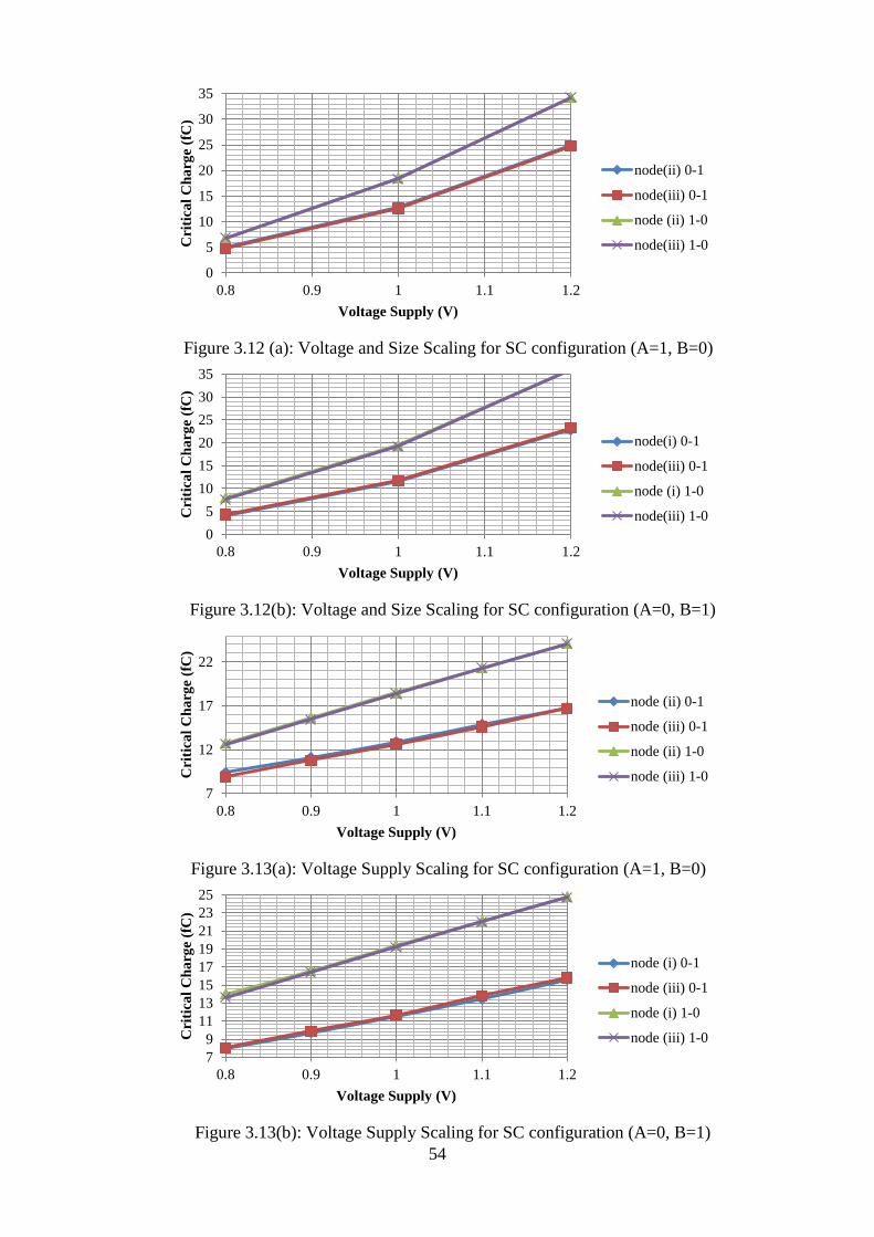
54
Figure 3.12 (a): Voltage and Size Scaling for SC configuration (A=1, B=0)
Figure 3.12(b): Voltage and Size Scaling for SC configuration (A=0, B=1)
Figure 3.13(a): Voltage Supply Scaling for SC configuration (A=1, B=0)
Figure 3.13(b): Voltage Supply Scaling for SC configuration (A=0, B=1)
0
5
10
15
20
25
30
35
0.8 0.9 1 1.1 1.2
Cri
tica
l C
ha
rge
(fC
)
Voltage Supply (V)
node(ii) 0-1
node(iii) 0-1
node (ii) 1-0
node(iii) 1-0
0
5
10
15
20
25
30
35
0.8 0.9 1 1.1 1.2
Cri
tica
l C
ha
rge
(fC
)
Voltage Supply (V)
node(i) 0-1
node(iii) 0-1
node (i) 1-0
node(iii) 1-0
7
12
17
22
0.8 0.9 1 1.1 1.2
Cri
tica
l C
ha
rge
(fC
)
Voltage Supply (V)
node (ii) 0-1
node (iii) 0-1
node (ii) 1-0
node (iii) 1-0
7
9
11
13
15
17
19
21
23
25
0.8 0.9 1 1.1 1.2
Cri
tica
l C
ha
rge
(fC
)
Voltage Supply (V)
node (i) 0-1
node (iii) 0-1
node (i) 1-0
node (iii) 1-0

55
Figure 3.14(a) : Size Scaling for SC configuration (A=1, B=0)
Figure 3.14(b) : Size Scaling for SC configuration (A=0, B=1)
3.3.3 Critical Charge Analysis for Single Rail Symmetric Implementation
Configuration
A Single rail symmetric configuration (SS) is similar to SC
implementation. It consists of main pull up transistors (P1,P2,P3,P4), pull
down transistors (N1,N2,N3,N4), inverter (P5,N5) and feedback transistors
(P6,N6) as shown in Figure 3.15 [50]. The feedback transistors should be
made as small as possible to reduce the loading effect. The symmetrical
structure gives an advantage with respect to the speed that due to the
symmetrical design. Suppose both inputs A and B are low cause the pull up
transistors to change the output Out to low. Similarly, if both inputs A and B
are both high causing the pull down transistors change the output Out to high.
If the inputs are not equal, and Out =0, the output is retained by a conducting
paths either transistors P1, P6, P4 or transistors P2, P6, P3. Symmetrically, if
the inputs are not equal, and Out =1, the output is retained by a conducting
path either transistors N1, N6, N4 or transistors N2, N6, N3. Current is
injected at nodes (i), (ii), (iii), (iv) and (v) and the state change at node Out is
0
5
10
15
20
25
30
50% 70% 90% 110% 130% 150%
Cri
tica
l C
ha
rge
(fC
)
Size
node (ii) 0-1
node (iii) 0-1
node (ii) 1-0
node (iii) 1-0
0
5
10
15
20
25
30
50% 70% 90% 110% 130% 150%
Cri
tica
l C
ha
rge
(fC
)
Size
node (i) 0-1
node (iii) 0-1
node (i) 1-0
node (iii) 1-0
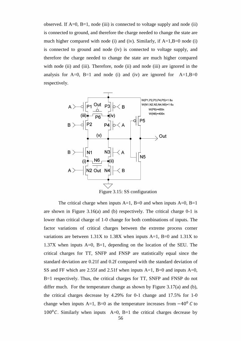
56
observed. If A=0, B=1, node (iii) is connected to voltage supply and node (ii)
is connected to ground, and therefore the charge needed to change the state are
much higher compared with node (i) and (iv). Similarly, if A=1,B=0 node (i)
is connected to ground and node (iv) is connected to voltage supply, and
therefore the charge needed to change the state are much higher compared
with node (ii) and (iii). Therefore, node (ii) and node (iii) are ignored in the
analysis for A=0, B=1 and node (i) and (iv) are ignored for A=1,B=0
respectively.
Figure 3.15: SS configuration
The critical charge when inputs A=1, B=0 and when inputs A=0, B=1
are shown in Figure 3.16(a) and (b) respectively. The critical charge 0-1 is
lower than critical charge of 1-0 change for both combinations of inputs. The
factor variations of critical charges between the extreme process corner
variations are between 1.31X to 1.38X when inputs A=1, B=0 and 1.31X to
1.37X when inputs A=0, B=1, depending on the location of the SEU. The
critical charges for TT, SNFP and FNSP are statistically equal since the
standard deviation are 0.21f and 0.2f compared with the standard deviation of
SS and FF which are 2.55f and 2.51f when inputs A=1, B=0 and inputs A=0,
B=1 respectively. Thus, the critical charges for TT, SNFP and FNSP do not
differ much. For the temperature change as shown by Figure 3.17(a) and (b),
the critical charges decrease by 4.29% for 0-1 change and 17.5% for 1-0
change when inputs A=1, B=0 as the temperature increases from −400 𝐶 to
1000𝐶 . Similarly when inputs A=0, B=1 the critical charges decrease by

57
5.9% for 0-1 change and 15.65% for 1-0 change on the same temperature
increment.
The effect of critical charges by scaling both voltage and size for SS is
shown in Figure 3.18(a) and (b). When A=1, B=0, the charges decrease by
49.7% when voltage and size are scaled from 1.2 V to 1 V and 150% to 100%
respectively and further decrease by 63.9% when voltage and size are scaled
from 1 V to 0.8 V and 100% to 50% respectively for 0-1 change. Similarly,
the charges decrease by 46.1% and further decrease by 63.9% with the same
scaling for 1-0 change. When A=0, B=1, the charges decrease by 48.9% when
voltage and size are scaled from 1.2 V to 1 V and 150% to 100% respectively
and further decrease by 64.3% when voltage and size are scaled from 1 V to
0.8 V and 100% to 50% respectively for 0-1 change. Similarly, the charges
decrease by 46.7% and further decrease by 62.9% with the same scaling for 1-
0 change.
With voltage scaling keeping constant nominal size as shown in Figure
3.19(a) and (b), when A=1,B=0, the critical charges needed to change the state
decrease by 48.3% and 47.2% as the voltage is scaled from 1.2 V to 0.8 V for
0-1 and 1-0 respectively. When A=0,B=1, the critical charges needed to
change the state decrease by 48.1% and 47.3% as the voltage is scaled from
1.2 V to 0.8 V for 0-1 and 1-0 respectively. The critical charges with size
scaling keeping constant nominal voltage are as shown in Figure 3.20(a) and
(b). When A=1,B=0, the critical charges needed to change the state from 0-1
increase by 48.7% as the size is scaled from 100% to 150% and decrease by
47.5% as the size is scaled from 100% to 50%. Similarly, the critical charges
needed to change the state from 1-0 increase by 42.8 % as the size is scaled
from 100% to 150% and decrease by 48.1% as the size is scaled from 100% to
50%. When A=0,B=1, the critical charges needed to change the state from 0-1
increase by 47.4% as the size is scaled from 100% to 150% and decrease by
48.5% as the size is scaled from 100% to 50%. Similarly, the critical charges
needed to change the state from 1-0 increase by 44.6% as the size is scaled
from 100% to 150% and decrease by 46.7% as the size is scaled from 100% to
50%.
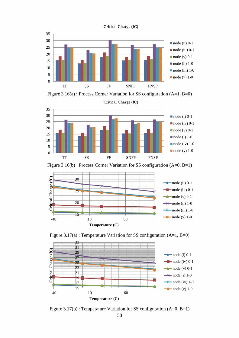
58
Figure 3.16(a) : Process Corner Variation for SS configuration (A=1, B=0)
Figure 3.16(b) : Process Corner Variation for SS configuration (A=0, B=1)
Figure 3.17(a) : Temperature Variation for SS configuration (A=1, B=0)
Figure 3.17(b) : Temperature Variation for SS configuration (A=0, B=1)
0
5
10
15
20
25
30
35
TT SS FF SNFP FNSP
Critical Charge (fC)
node (ii) 0-1
node (iii) 0-1
node (v) 0-1
node (ii) 1-0
node (iii) 1-0
node (v) 1-0
0
5
10
15
20
25
30
35
TT SS FF SNFP FNSP
Critical Charge (fC)
node (i) 0-1
node (iv) 0-1
node (v) 0-1
node (i) 1-0
node (iv) 1-0
node (v) 1-0
15
20
25
30
-40 10 60
Cri
tica
l C
ha
rge
(fC
)
Temperature (C)
node (ii) 0-1
node (iii) 0-1
node (v) 0-1
node (ii) 1-0
node (iii) 1-0
node (v) 1-0
15
17
19
21
23
25
27
29
31
33
-40 10 60
Cri
tica
l C
ha
rge
(fC
)
Temperature (C)
node (i) 0-1
node (iv) 0-1
node (v) 0-1
node (i) 1-0
node (iv) 1-0
node (v) 1-0

59
Figure 3.18(a): Voltage and Size Scaling for SS configuration (A=1, B=0)
Figure 3.18(b): Voltage and Size Scaling for SS configuration (A=0, B=1)
Figure 3.19(a): Voltage Supply Scaling for SS configuration (A=1, B=0)
Figure 3.19(b): Voltage Supply Scaling for SS configuration (A=0, B=1)
0
10
20
30
40
50
60
0.8 0.9 1 1.1 1.2
Cri
tica
l C
ha
rge
(fC
)
Voltage Supply (V)
node(ii) 0-1
node(iii) 0-1
node(v) 0-1
node(ii) 1-0
node(iii) 1-0
node(v) 1-0
0
10
20
30
40
50
60
0.8 0.9 1 1.1 1.2
Cri
tica
l C
ha
rge
(fC
)
Voltage Supply (V)
node(i) 0-1
node(iv) 0-1
node(v) 0-1
node(i) 1-0
node(iv) 1-0
node(v) 1-0
10
15
20
25
30
35
0.8 0.9 1 1.1 1.2
Cri
tica
l C
ha
rge
(fC
)
Voltage Supply (V)
node (ii) 0-1
node (iii) 0-1
node (v) 0-1
node (ii) 1-0
node (iii) 1-0
node (v) 1-0
10
15
20
25
30
35
0.8 0.9 1 1.1 1.2
Cri
tica
l C
ha
rge
(fC
)
Voltage Supply (V)
node (i) 0-1
node (iv) 0-1
node (v) 0-1
node (i) 1-0
node (vi) 1-0
node (v) 1-0
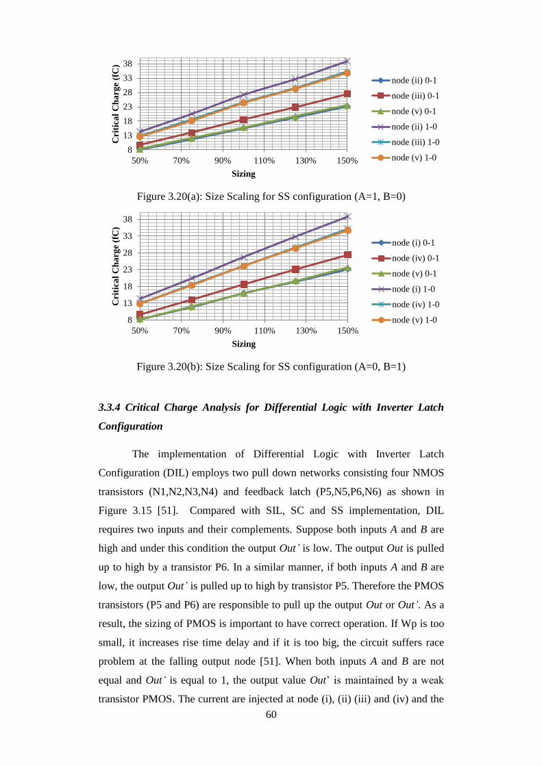
60
Figure 3.20(a): Size Scaling for SS configuration (A=1, B=0)
Figure 3.20(b): Size Scaling for SS configuration (A=0, B=1)
3.3.4 Critical Charge Analysis for Differential Logic with Inverter Latch
Configuration
The implementation of Differential Logic with Inverter Latch
Configuration (DIL) employs two pull down networks consisting four NMOS
transistors (N1,N2,N3,N4) and feedback latch (P5,N5,P6,N6) as shown in
Figure 3.15 [51]. Compared with SIL, SC and SS implementation, DIL
requires two inputs and their complements. Suppose both inputs A and B are
high and under this condition the output Out’ is low. The output Out is pulled
up to high by a transistor P6. In a similar manner, if both inputs A and B are
low, the output Out’ is pulled up to high by transistor P5. Therefore the PMOS
transistors (P5 and P6) are responsible to pull up the output Out or Out’. As a
result, the sizing of PMOS is important to have correct operation. If Wp is too
small, it increases rise time delay and if it is too big, the circuit suffers race
problem at the falling output node [51]. When both inputs A and B are not
equal and Out’ is equal to 1, the output value Out’ is maintained by a weak
transistor PMOS. The current are injected at node (i), (ii) (iii) and (iv) and the
8
13
18
23
28
33
38
50% 70% 90% 110% 130% 150%
Cri
tica
l C
ha
rge
(fC
)
Sizing
node (ii) 0-1
node (iii) 0-1
node (v) 0-1
node (ii) 1-0
node (iii) 1-0
node (v) 1-0
8
13
18
23
28
33
38
50% 70% 90% 110% 130% 150%
Cri
tica
l C
ha
rge
(fC
)
Sizing
node (i) 0-1
node (iv) 0-1
node (v) 0-1
node (i) 1-0
node (iv) 1-0
node (v) 1-0

61
state change at node Out is observed depending on the inputs combination. If
A=0, B=1, node (i) is connected to voltage supply, and therefore the charge
needed to change the state are much higher compared with node (ii). Similarly,
if A=1,B=0 node (ii) is connected to ground, and therefore the charge needed
to change the state are much higher compared with node (i).
Figure 3.21: DIL configuration
The critical charge when inputs A=1, B=0 and when inputs A=0, B=1
are shown in Figure 3.22(a) and (b) respectively. The critical charge 0-1 is
lower than critical charge of 1-0 change for A=1, B=0 and the opposite for
A=0, B=1. The factors variation of critical charges between the extreme
process corner variations is 1.5X and 1.25X for A=1,B=0 and A=0,B=1. The
critical charges for TT, SNFP and FNSP are statistically equal since the
standard deviation are 0.48f and 0.81f compared with the standard deviation of
SS and FF which are 3.93f and 4.38f when inputs A=1, B=0 and inputs A=0,
B=1 respectively. Thus, the critical charges for TT, SNFP and FNSP do not
differ much. It can be concluded that critical charges on DIL are very sensitive
to the process variation. For the temperature change as shown by Figure
3.23(a) and (b), the critical charges decrease by 11.1% for 0-1 change and
18.3% for 1-0 change when inputs A=1, B=0 as the temperature increases
from −400 𝐶 to 1000𝐶. Similarly when inputs A=0, B=1 the critical charges
decrease by 17.8% for 0-1 change and 12.2% for 1-0 change on the same
temperature increment.
As with others configurations, the DIL configuration is also scaled
both voltage and size to investigate the effect of critical charges as shown in

62
Figure 3.24(a) and (b). When A=1, B=0, the charges decrease by 50.4% when
voltage and size are scaled from 1.2 V to 1 V and 150% to 100% respectively
and further decrease by 64.7% when voltage and size are scaled from 1 V to
0.8 V and 100% to 50% respectively for 0-1 change. Similarly, the charges
decrease by 47.7% and further decrease by 60.4% with the same scaling for 1-
0 change. When A=0, B=1, the charges decrease by 47.4% when voltage and
size are scaled from 1.2 V to 1 V and 150% to 100% respectively and further
decrease by 58.5% when voltage and size are scaled from 1 V to 0.8 V and
100% to 50% respectively for 0-1 change. Similarly, the charges decrease by
51.2% and further decrease by 64.7% with the same scaling for 1-0 change.
With voltage scaling keeping constant nominal size as shown in Figure
3.25(a) and (b), when A=1,B=0, the critical charges needed to change the state
decrease by 52.5% and 42.7% as the voltage is scaled from 1.2 V to 0.8 V for
0-1 and 1-0 respectively. When A=0,B=1, the critical charges needed to
change the state decrease by 42.2% and 52.8% as the voltage is scaled from
1.2 V to 0.8 V for 0-1 and 1-0 respectively. The critical charges with size
scaling keeping constant nominal voltage are as shown in Figure 3.26(a) and
(b). When A=1,B=0, the critical charges needed to change the state from 0-1
increase by 44.9% as the size is scaled from 100% to 150% and decrease by
47.3% as the size is scaled from 100% to 50%. Similarly, the critical charges
needed to change the state from 1-0 increase by 47.9 % as the size is scaled
from 100% to 150% and decrease by 46.8% as the size is scaled from 100% to
50%. When A=0,B=1, the critical charges needed to change the state from 0-1
increase by 48.7% as the size is scaled from 100% to 150% and decrease by
44.9% as the size is scaled from 100% to 50%. Similarly, the critical charges
needed to change the state from 1-0 increase by 46.1% as the size is scaled
from 100% to 150% and decrease by 46.4% as the size is scaled from 100% to
50%.
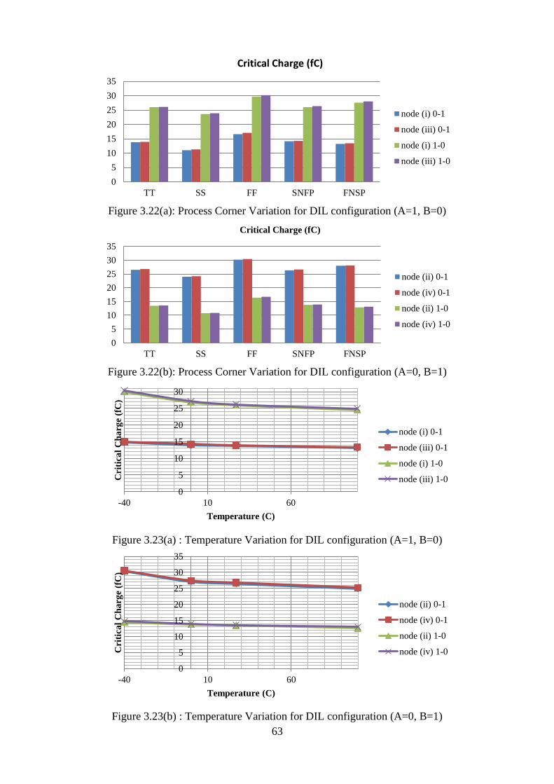
63
Figure 3.22(a): Process Corner Variation for DIL configuration (A=1, B=0)
Figure 3.22(b): Process Corner Variation for DIL configuration (A=0, B=1)
Figure 3.23(a) : Temperature Variation for DIL configuration (A=1, B=0)
Figure 3.23(b) : Temperature Variation for DIL configuration (A=0, B=1)
0
5
10
15
20
25
30
35
TT SS FF SNFP FNSP
Critical Charge (fC)
node (i) 0-1
node (iii) 0-1
node (i) 1-0
node (iii) 1-0
0
5
10
15
20
25
30
35
TT SS FF SNFP FNSP
Critical Charge (fC)
node (ii) 0-1
node (iv) 0-1
node (ii) 1-0
node (iv) 1-0
0
5
10
15
20
25
30
-40 10 60
Cri
tica
l C
ha
rge
(fC
)
Temperature (C)
node (i) 0-1
node (iii) 0-1
node (i) 1-0
node (iii) 1-0
0
5
10
15
20
25
30
35
-40 10 60
Cri
tica
l C
ha
rge
(fC
)
Temperature (C)
node (ii) 0-1
node (iv) 0-1
node (ii) 1-0
node (iv) 1-0
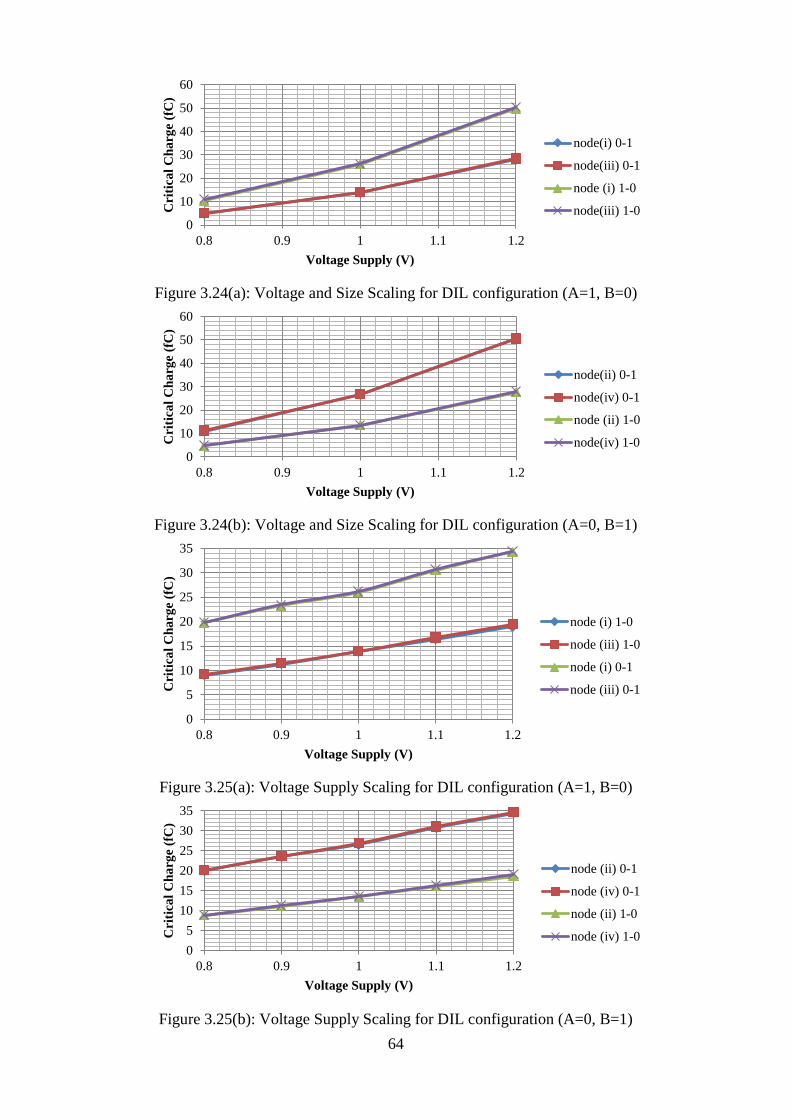
64
Figure 3.24(a): Voltage and Size Scaling for DIL configuration (A=1, B=0)
Figure 3.24(b): Voltage and Size Scaling for DIL configuration (A=0, B=1)
Figure 3.25(a): Voltage Supply Scaling for DIL configuration (A=1, B=0)
Figure 3.25(b): Voltage Supply Scaling for DIL configuration (A=0, B=1)
0
10
20
30
40
50
60
0.8 0.9 1 1.1 1.2
Cri
tica
l C
ha
rge
(fC
)
Voltage Supply (V)
node(i) 0-1
node(iii) 0-1
node (i) 1-0
node(iii) 1-0
0
10
20
30
40
50
60
0.8 0.9 1 1.1 1.2
Cri
tica
l C
ha
rge
(fC
)
Voltage Supply (V)
node(ii) 0-1
node(iv) 0-1
node (ii) 1-0
node(iv) 1-0
0
5
10
15
20
25
30
35
0.8 0.9 1 1.1 1.2
Cri
tica
l C
ha
rge
(fC
)
Voltage Supply (V)
node (i) 1-0
node (iii) 1-0
node (i) 0-1
node (iii) 0-1
0
5
10
15
20
25
30
35
0.8 0.9 1 1.1 1.2
Cri
tica
l C
ha
rge
(fC
)
Voltage Supply (V)
node (ii) 0-1
node (iv) 0-1
node (ii) 1-0
node (iv) 1-0

65
Figure 3.26(a) : Size Scaling for DIL configuration (A=1, B=0)
Figure 3.26(b) : Size Scaling for DIL configuration (A=0, B=1)
3.4 Circuit Vulnerability Against Single Event Upset -Critical Charge
In this section, the values of standard deviation are used in order to
compare the vulnerability of C-elements with respect of SEU. These values
are used to investigate the node sensitivity towards SEU as different factors
changes and to show how the critical charges change with respect to the
parameter changes.
The nodes sensitivity of different configurations of C-elements with
respect to the process variation, temperature, voltage and size scaling are
presented as shown in Figure 3.27-3.31 when A=1, B=0. The nodes sensitivity
are obtained by calculating the standard deviation of the critical charge on
every nodes in C-elements. The formulae of standard deviation can be found
in Appendix A. The purpose is to observe the dispersion value of critical
change when one of the factors as mention above is changing. It is observed
that size scaling has the highest standard deviation and temperature has the
lowest standard deviation as shown in Figure 3.28(a) and (b) and Figure
3.31(a) and (b) respectively. This observation shows that the most effective
0
5
10
15
20
25
30
35
40
50% 70% 90% 110% 130% 150%
Cri
tica
l C
ha
rge
(fC
)
Sizing
node (i) 0-1
node (iii) 0-1
node (i) 1-0
node (iii) 1-0
0
5
10
15
20
25
30
35
40
50% 70% 90% 110% 130% 150%
Cri
tica
l C
ha
rge
(fC
)
Sizing
node (ii) 0-1
node (iv) 0-1
node (ii) 1-0
node (iv) 1-0
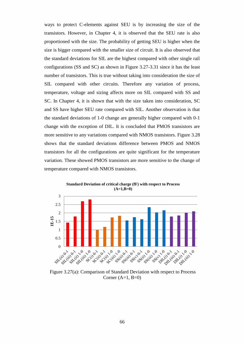
66
ways to protect C-elements against SEU is by increasing the size of the
transistors. However, in Chapter 4, it is observed that the SEU rate is also
proportioned with the size. The probability of getting SEU is higher when the
size is bigger compared with the smaller size of circuit. It is also observed that
the standard deviations for SIL are the highest compared with other single rail
configurations (SS and SC) as shown in Figure 3.27-3.31 since it has the least
number of transistors. This is true without taking into consideration the size of
SIL compared with other circuits. Therefore any variation of process,
temperature, voltage and sizing affects more on SIL compared with SS and
SC. In Chapter 4, it is shown that with the size taken into consideration, SC
and SS have higher SEU rate compared with SIL. Another observation is that
the standard deviations of 1-0 change are generally higher compared with 0-1
change with the exception of DIL. It is concluded that PMOS transistors are
more sensitive to any variations compared with NMOS transistors. Figure 3.28
shows that the standard deviations difference between PMOS and NMOS
transistors for all the configurations are quite significant for the temperature
variation. These showed PMOS transistors are more sensitive to the change of
temperature compared with NMOS transistors.
Figure 3.27(a): Comparison of Standard Deviation with respect to Process
Corner (A=1, B=0)
0
0.5
1
1.5
2
2.5
3
1E
-15
Standard Deviation of critical charge (fF) with respect to Process
(A=1,B=0)
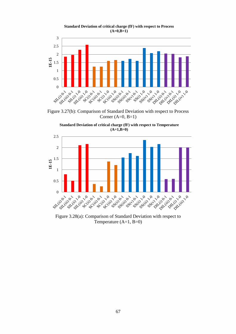
67
Figure 3.27(b): Comparison of Standard Deviation with respect to Process
Corner (A=0, B=1)
Figure 3.28(a): Comparison of Standard Deviation with respect to
Temperature (A=1, B=0)
0
0.5
1
1.5
2
2.5
3
1E
-15
Standard Deviation of critical charge (fF) with respect to Process
(A=0,B=1)
0
0.5
1
1.5
2
2.5
1E
-15
Standard Deviation of critical charge (fF) with respect to Temperature
(A=1,B=0)
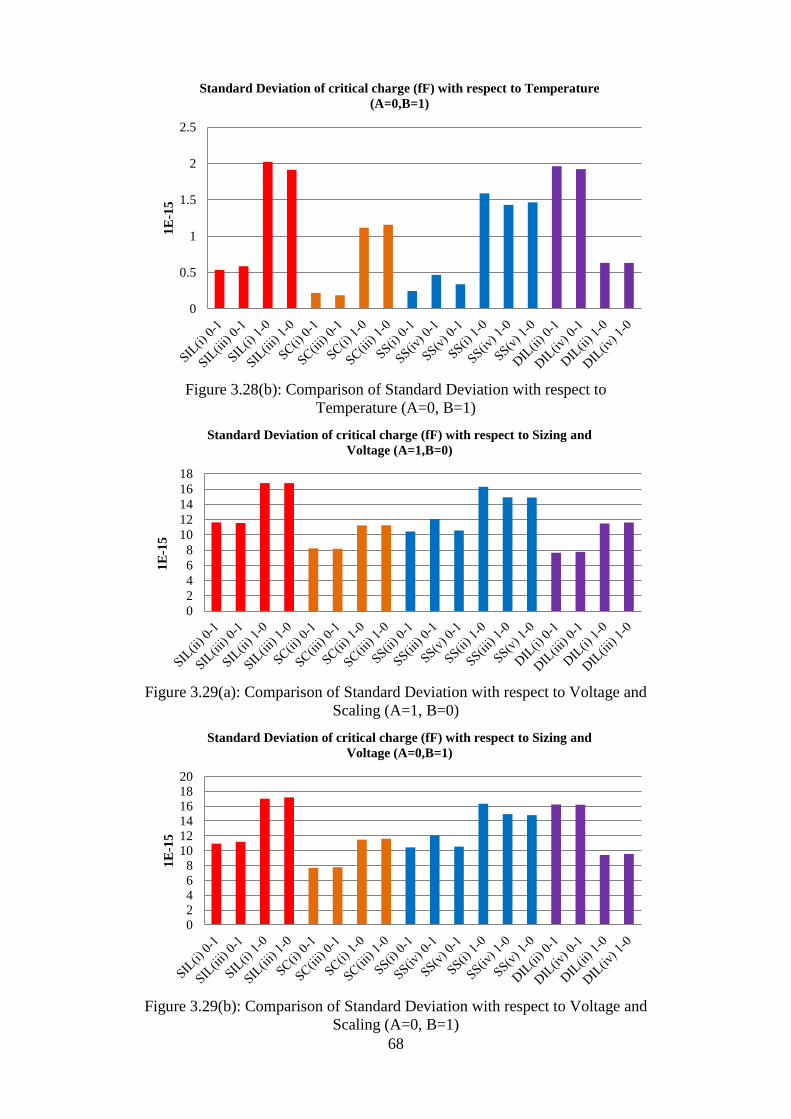
68
Figure 3.28(b): Comparison of Standard Deviation with respect to
Temperature (A=0, B=1)
Figure 3.29(a): Comparison of Standard Deviation with respect to Voltage and
Scaling (A=1, B=0)
Figure 3.29(b): Comparison of Standard Deviation with respect to Voltage and
Scaling (A=0, B=1)
0
0.5
1
1.5
2
2.5
1E
-15
Standard Deviation of critical charge (fF) with respect to Temperature
(A=0,B=1)
0
2
4
6
8
10
12
14
16
18
1E
-15
Standard Deviation of critical charge (fF) with respect to Sizing and
Voltage (A=1,B=0)
02468
101214161820
1E
-15
Standard Deviation of critical charge (fF) with respect to Sizing and
Voltage (A=0,B=1)

69
Figure 3.30(a): Comparison of Standard Deviation with respect to Voltage
Scaling (A=1, B=0)
Figure 3.30(b): Comparison of Standard Deviation with respect to Voltage
Scaling (A=0, B=1)
0
1
2
3
4
5
6
7
1E
-15
Standard Deviation of critical charge (fF) with respect to Voltage
(A=1,B=0)
0
1
2
3
4
5
6
7
1E
-15
Standard Deviation of critical charge (fF) with respect to Voltage
(A=0,B=1)
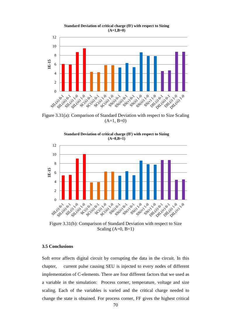
70
Figure 3.31(a): Comparison of Standard Deviation with respect to Size Scaling
(A=1, B=0)
Figure 3.31(b): Comparison of Standard Deviation with respect to Size
Scaling (A=0, B=1)
3.5 Conclusions
Soft error affects digital circuit by corrupting the data in the circuit. In this
chapter, current pulse causing SEU is injected to every nodes of different
implementation of C-elements. There are four different factors that we used as
a variable in the simulation: Process corner, temperature, voltage and size
scaling. Each of the variables is varied and the critical charge needed to
change the state is obtained. For process corner, FF gives the highest critical
0
2
4
6
8
10
12
1E
-15
Standard Deviation of critical charge (fF) with respect to Sizing
(A=1,B=0)
0
2
4
6
8
10
12
1E
-15
Standard Deviation of critical charge (fF) with respect to Sizing
(A=0,B=1)
71
charges due to the larger pull up and pull down strength of transistors. As a
result, the strength of transistors give better stabilization in the voltage level of
the storage node and hence higher critical charge is needed to flip the output.
For temperature, as temperature increases, it degrades the threshold voltage,
carrier mobility and saturation velocity As a result of degrading carrier
mobility, the drain current becomes lower and the sensitivity of the node
towards SEU is increased. Hence, the critical charge needed to flip the output
is decreased. For voltage, as voltage decrease, the critical charge needed to
change the state also decreased. As a result, the stored charge needed to flip
the output is also reduced. Finally, for size, reducing the size of the transistors
decrease the gate capacitance from the output and therefore the collected
charge needed to flip the output is also becoming smaller
It is observed that size is the most important factors of critical charge
variation since it has the highest standard deviation compared with others
factors. This is due to the increasing the size of the transistors increase the gate
capacitance from the output and therefore the collected charge needed to flip
the output is also larger. However, as the size of the circuit is bigger, the
probability of hitting by SEU is also increased even though the circuit is more
resistant against SEU. This is discussed in chapter 4. The least significant
factor is the temperature. As the temperature increased, the mobility of the
carrier is reduced and degrades the performance of the transistor. It is also
observed that the standard deviations for SIL are the highest compared with
other single rail configurations (SS and SC) since it has the least number of
transistors. This is true without taking into consideration the size of SIL
compared with other circuits.

72
Chapter 4. Error Rate Analysis of Different Configurations of
C-elements
This chapter presents an analysis of soft error rate on vulnerable nodes. A new
method is developed to calculate the error rate of the four different C-element
circuits. The total error rates with respect to process corner, temperature,
voltage, and size scaling of the circuits are compared. From the error rate
values, a comparison of vulnerability towards SEU with different
configurations of C-elements can be made with respect to the change of the
four factors above.
4.1 Introduction
In Chapter 3, the nodes are injected with the current pulse causing SEU
and the critical charges are obtained on each node of C-elements. Different
configurations of C-elements have been compared in term of the critical
charges needed to flip the output and the standard deviation of critical charges.
However, in order to accurately compare the vulnerability of C-elements, the
error rate due to SEU in four different C-elements need to be obtained. As the
values lies between low to high, no clear interpretation by the circuit or system
on this value that lead to circuit malfunction In this chapter, a method of
calculating error rate of different configurations is proposed by taking into
account the values lies between low to high.
Previous chapter considered the responses of the state holders by
observing only the change of the state holder from 1-0 change or 0-1 change.
In this chapter, all of the responses of the state holders are considered:
a) No change to the state holder – There is insignificant output pulse that
has been generated and does not cause any state change. It is assumed
that if the generated pulse is less than 20% [52] of the input pulse such
pulse can be further attenuated in the following gates and caused no
further damage. This is shown in Figure 4.1 (a) and Figure 4.2(a).
b) Pulse output is generated- Over a small range of input pulse amplitude,
the pulse output is generated. It is assumed that if the generated pulse
is 20% [52] or more of the input pulse, such pulse can be very likely to
cause the problem. This is shown in Figure 4.1(b) and Figure 4.2(b)

73
c) State change – At certain amplitude of current pulse, the state holder
can change its state. This is shown in Figure 4.1 (c) and Figure 4.2(c)
Figure 4.1: State holder change from
low to high (0-1)
Figure 4.2: State holder change from
high to low (1-0)
4.2 Mathematical Modelling of Soft Error
For simplicity, an injected current that resemble SEU is assumed to
have trapezoidal shape with width (𝑡𝑤), fast rising time (𝑡𝑟), slow falling time
(𝑡𝑓) and an amplitude 𝐴𝑚𝑝𝑖 . Let 𝐴𝑚𝑝1 be an amplitude of injected pulse in
such a way that produce Out(t) ≥ 0.2 and 𝐴𝑚𝑝2 is the amplitude of injected
pulse that cause the output to corrupt or change the state to change. Since the
generated pulse directly proportion with the ratio of the injected charge that
produced Out(t) ≥ 0.2, (𝑄𝑖𝑛𝑗𝑒𝑐𝑡𝑒𝑑), with the injected charge that cause the
state to change, (𝑄𝑠𝑡𝑎𝑡𝑒−𝑐ℎ𝑎𝑛𝑔𝑒), the mathematical expressions are derived to
describe the response of the state holders as illustrated as above. Furthermore,
whether the state is corrupted or not is depended on the polarity of the current
source. The positive polarity of current on n-type drain can cause the state to
change from 1-0-1. The negative polarity on n-type drain can only reinforce
logic state 1 [53]. Therefore, by taking into consideration the polarity of
current, a constant 1
2 is added to the response equation to indicate that there are
50% chances of current to cause SEU. The response of the state holder
equation is given by 4.1
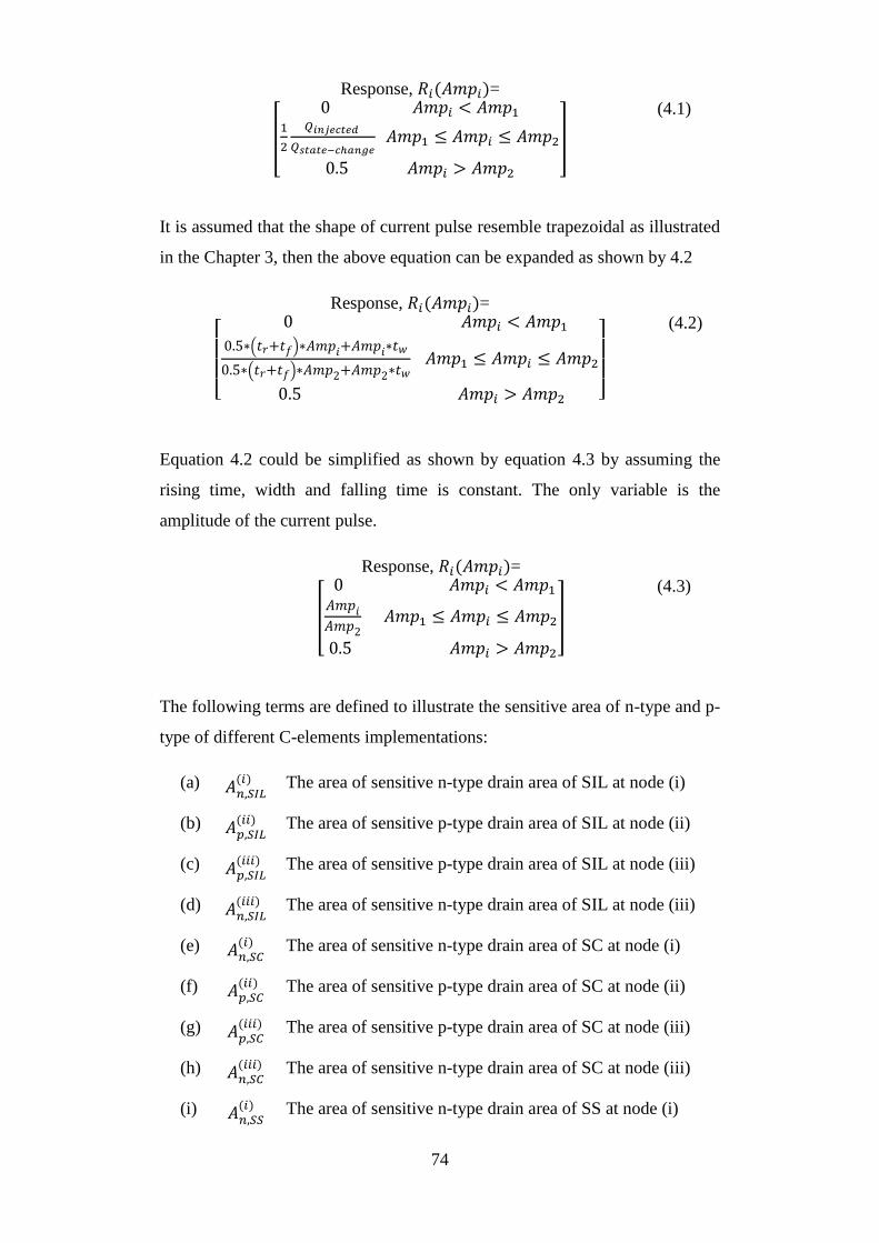
74
Response, 𝑅𝑖(𝐴𝑚𝑝𝑖)=
[
0 𝐴𝑚𝑝𝑖 < 𝐴𝑚𝑝11
2
𝑄𝑖𝑛𝑗𝑒𝑐𝑡𝑒𝑑
𝑄𝑠𝑡𝑎𝑡𝑒−𝑐ℎ𝑎𝑛𝑔𝑒 𝐴𝑚𝑝1 ≤ 𝐴𝑚𝑝𝑖 ≤ 𝐴𝑚𝑝2
0.5 𝐴𝑚𝑝𝑖 > 𝐴𝑚𝑝2
]
(4.1)
It is assumed that the shape of current pulse resemble trapezoidal as illustrated
in the Chapter 3, then the above equation can be expanded as shown by 4.2
Response, 𝑅𝑖(𝐴𝑚𝑝𝑖)=
[
0 𝐴𝑚𝑝𝑖 < 𝐴𝑚𝑝10.5∗(𝑡𝑟+𝑡𝑓)∗𝐴𝑚𝑝𝑖+𝐴𝑚𝑝𝑖∗𝑡𝑤
0.5∗(𝑡𝑟+𝑡𝑓)∗𝐴𝑚𝑝2+𝐴𝑚𝑝2∗𝑡𝑤 𝐴𝑚𝑝1 ≤ 𝐴𝑚𝑝𝑖 ≤ 𝐴𝑚𝑝2
0.5 𝐴𝑚𝑝𝑖 > 𝐴𝑚𝑝2 ]
(4.2)
Equation 4.2 could be simplified as shown by equation 4.3 by assuming the
rising time, width and falling time is constant. The only variable is the
amplitude of the current pulse.
Response, 𝑅𝑖(𝐴𝑚𝑝𝑖)=
[
0 𝐴𝑚𝑝𝑖 < 𝐴𝑚𝑝1𝐴𝑚𝑝𝑖𝐴𝑚𝑝2
𝐴𝑚𝑝1 ≤ 𝐴𝑚𝑝𝑖 ≤ 𝐴𝑚𝑝2
0.5 𝐴𝑚𝑝𝑖 > 𝐴𝑚𝑝2
]
(4.3)
The following terms are defined to illustrate the sensitive area of n-type and p-
type of different C-elements implementations:
(a) 𝐴𝑛,𝑆𝐼𝐿(𝑖)
The area of sensitive n-type drain area of SIL at node (i)
(b) 𝐴𝑝,𝑆𝐼𝐿(𝑖𝑖)
The area of sensitive p-type drain area of SIL at node (ii)
(c) 𝐴𝑝,𝑆𝐼𝐿(𝑖𝑖𝑖)
The area of sensitive p-type drain area of SIL at node (iii)
(d) 𝐴𝑛,𝑆𝐼𝐿(𝑖𝑖𝑖)
The area of sensitive n-type drain area of SIL at node (iii)
(e) 𝐴𝑛,𝑆𝐶(𝑖)
The area of sensitive n-type drain area of SC at node (i)
(f) 𝐴𝑝,𝑆𝐶(𝑖𝑖)
The area of sensitive p-type drain area of SC at node (ii)
(g) 𝐴𝑝,𝑆𝐶(𝑖𝑖𝑖)
The area of sensitive p-type drain area of SC at node (iii)
(h) 𝐴𝑛,𝑆𝐶(𝑖𝑖𝑖)
The area of sensitive n-type drain area of SC at node (iii)
(i) 𝐴𝑛,𝑆𝑆(𝑖)
The area of sensitive n-type drain area of SS at node (i)
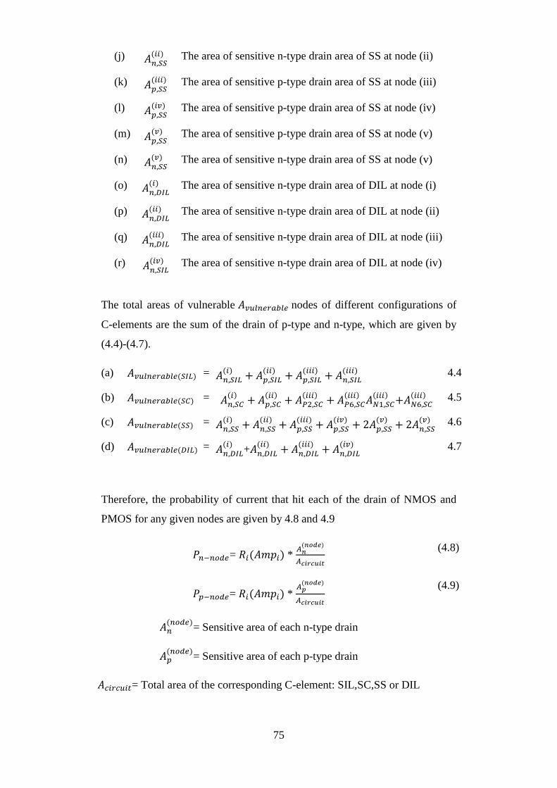
75
(j) 𝐴𝑛,𝑆𝑆(𝑖𝑖)
The area of sensitive n-type drain area of SS at node (ii)
(k) 𝐴𝑝,𝑆𝑆(𝑖𝑖𝑖)
The area of sensitive p-type drain area of SS at node (iii)
(l) 𝐴𝑝,𝑆𝑆(𝑖𝑣)
The area of sensitive p-type drain area of SS at node (iv)
(m) 𝐴𝑝,𝑆𝑆(𝑣)
The area of sensitive p-type drain area of SS at node (v)
(n) 𝐴𝑛,𝑆𝑆(𝑣)
The area of sensitive n-type drain area of SS at node (v)
(o) 𝐴𝑛,𝐷𝐼𝐿(𝑖)
The area of sensitive n-type drain area of DIL at node (i)
(p) 𝐴𝑛,𝐷𝐼𝐿(𝑖𝑖)
The area of sensitive n-type drain area of DIL at node (ii)
(q) 𝐴𝑛,𝐷𝐼𝐿(𝑖𝑖𝑖)
The area of sensitive n-type drain area of DIL at node (iii)
(r) 𝐴𝑛,𝑆𝐼𝐿(𝑖𝑣)
The area of sensitive n-type drain area of DIL at node (iv)
The total areas of vulnerable 𝐴𝑣𝑢𝑙𝑛𝑒𝑟𝑎𝑏𝑙𝑒 nodes of different configurations of
C-elements are the sum of the drain of p-type and n-type, which are given by
(4.4)-(4.7).
(a) 𝐴𝑣𝑢𝑙𝑛𝑒𝑟𝑎𝑏𝑙𝑒(𝑆𝐼𝐿) = 𝐴𝑛,𝑆𝐼𝐿(𝑖)
+ 𝐴𝑝,𝑆𝐼𝐿(𝑖𝑖)
+ 𝐴𝑝,𝑆𝐼𝐿(𝑖𝑖𝑖)
+ 𝐴𝑛,𝑆𝐼𝐿(𝑖𝑖𝑖)
4.4
(b) 𝐴𝑣𝑢𝑙𝑛𝑒𝑟𝑎𝑏𝑙𝑒(𝑆𝐶) = 𝐴𝑛,𝑆𝐶(𝑖) + 𝐴𝑝,𝑆𝐶
(𝑖𝑖) + 𝐴𝑃2,𝑆𝐶(𝑖𝑖𝑖) + 𝐴𝑃6,𝑆𝐶
(𝑖𝑖𝑖) 𝐴𝑁1,𝑆𝐶(𝑖𝑖𝑖) +𝐴𝑁6,𝑆𝐶
(𝑖𝑖𝑖) 4.5
(c) 𝐴𝑣𝑢𝑙𝑛𝑒𝑟𝑎𝑏𝑙𝑒(𝑆𝑆) = 𝐴𝑛,𝑆𝑆(𝑖)
+ 𝐴𝑛,𝑆𝑆(𝑖𝑖)
+ 𝐴𝑝,𝑆𝑆(𝑖𝑖𝑖)
+ 𝐴𝑝,𝑆𝑆(𝑖𝑣)
+ 2𝐴𝑝,𝑆𝑆(𝑣)
+ 2𝐴𝑛,𝑆𝑆(𝑣)
4.6
(d) 𝐴𝑣𝑢𝑙𝑛𝑒𝑟𝑎𝑏𝑙𝑒(𝐷𝐼𝐿) = 𝐴𝑛,𝐷𝐼𝐿(𝑖)
+𝐴𝑛,𝐷𝐼𝐿(𝑖𝑖)
+ 𝐴𝑛,𝐷𝐼𝐿(𝑖𝑖𝑖)
+ 𝐴𝑛,𝐷𝐼𝐿(𝑖𝑣)
4.7
Therefore, the probability of current that hit each of the drain of NMOS and
PMOS for any given nodes are given by 4.8 and 4.9
𝑃𝑛−𝑛𝑜𝑑𝑒= 𝑅𝑖(𝐴𝑚𝑝𝑖) * 𝐴𝑛(𝑛𝑜𝑑𝑒)
𝐴𝑐𝑖𝑟𝑐𝑢𝑖𝑡
(4.8)
𝑃𝑝−𝑛𝑜𝑑𝑒= 𝑅𝑖(𝐴𝑚𝑝𝑖) * 𝐴𝑝(𝑛𝑜𝑑𝑒)
𝐴𝑐𝑖𝑟𝑐𝑢𝑖𝑡
(4.9)
𝐴𝑛(𝑛𝑜𝑑𝑒)
= Sensitive area of each n-type drain
𝐴𝑝(𝑛𝑜𝑑𝑒)
= Sensitive area of each p-type drain
𝐴𝑐𝑖𝑟𝑐𝑢𝑖𝑡= Total area of the corresponding C-element: SIL,SC,SS or DIL
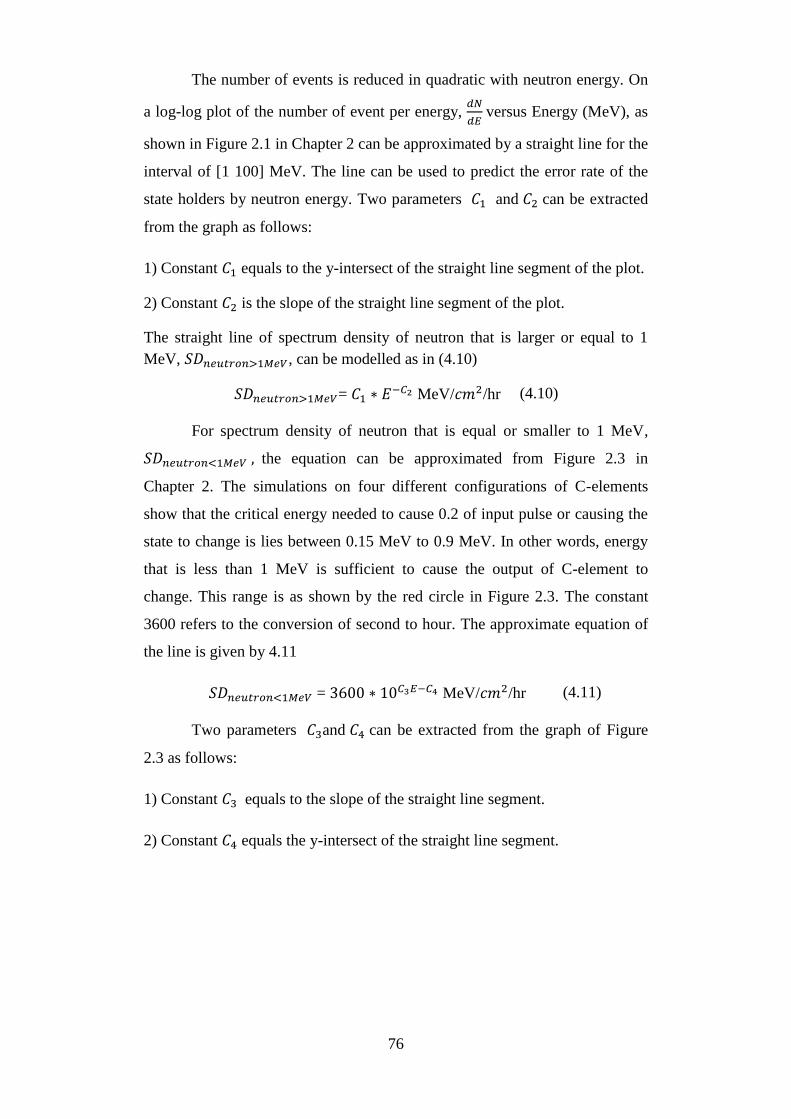
76
The number of events is reduced in quadratic with neutron energy. On
a log-log plot of the number of event per energy, 𝑑𝑁
𝑑𝐸 versus Energy (MeV), as
shown in Figure 2.1 in Chapter 2 can be approximated by a straight line for the
interval of [1 100] MeV. The line can be used to predict the error rate of the
state holders by neutron energy. Two parameters 𝐶1 and 𝐶2 can be extracted
from the graph as follows:
1) Constant 𝐶1 equals to the y-intersect of the straight line segment of the plot.
2) Constant 𝐶2 is the slope of the straight line segment of the plot.
The straight line of spectrum density of neutron that is larger or equal to 1
MeV, 𝑆𝐷𝑛𝑒𝑢𝑡𝑟𝑜𝑛>1𝑀𝑒𝑉, can be modelled as in (4.10)
𝑆𝐷𝑛𝑒𝑢𝑡𝑟𝑜𝑛>1𝑀𝑒𝑉= 𝐶1 ∗ 𝐸−𝐶2 MeV/𝑐𝑚2/hr
(4.10)
For spectrum density of neutron that is equal or smaller to 1 MeV,
𝑆𝐷𝑛𝑒𝑢𝑡𝑟𝑜𝑛<1𝑀𝑒𝑉 , the equation can be approximated from Figure 2.3 in
Chapter 2. The simulations on four different configurations of C-elements
show that the critical energy needed to cause 0.2 of input pulse or causing the
state to change is lies between 0.15 MeV to 0.9 MeV. In other words, energy
that is less than 1 MeV is sufficient to cause the output of C-element to
change. This range is as shown by the red circle in Figure 2.3. The constant
3600 refers to the conversion of second to hour. The approximate equation of
the line is given by 4.11
𝑆𝐷𝑛𝑒𝑢𝑡𝑟𝑜𝑛<1𝑀𝑒𝑉 = 3600 ∗ 10𝐶3𝐸−𝐶4 MeV/𝑐𝑚2/hr
(4.11)
Two parameters 𝐶3and 𝐶4 can be extracted from the graph of Figure
2.3 as follows:
1) Constant 𝐶3 equals to the slope of the straight line segment.
2) Constant 𝐶4 equals the y-intersect of the straight line segment.

77
Figure 4.3: Normalized atmospheric neutron cross section with the drain area
The ratio of normalized atmospheric neutron cross section with the
drain area of PMOS and NMOS with 0.1 𝜇𝑚 technologies for neutron energy
is shown in Figure 4.3[54]. As the 90 nm-technology is used in the simulation,
the ratio can be approximated by neutron cross section and drain cross section
with 0.1 𝜇𝑚 technology. It is very obvious from the graph that NMOS
transistor is more vulnerable towards SEU compared with PMOS transistor.
Karnik [17] suggested that for the same transistor width, NMOS transistor is
2.2 times more sensitive compared with PMOS transistor. This is due to the
collected charge for drain NMOS is higher for drain PMOS. The equations for
normalized cross section of PMOS and NMOS straight-line for 0.1 𝜇𝑚
technology are given by 4.12 and 4.13
𝑛𝑚𝑜𝑠𝑛𝑜𝑟𝑚𝑎𝑙𝑖𝑠𝑒𝑑 = 10(𝑑1𝑄+𝑑2) (4.12)
𝑝𝑚𝑜𝑠𝑛𝑜𝑟𝑚𝑎𝑙𝑖𝑠𝑒𝑑 = 10(𝑒1𝑄+𝑒2)
(4.13)
𝑑1, 𝑑2, 𝑒1and 𝑒2 are constants
Four parameters 𝑑1, 𝑑2,𝑒1and 𝑒2 can be extracted from the graph of
Figure 4.3 as follows:
1) Constant 𝑑1 and 𝑒1 equal to the slope of the straight line segment of nmos
and pmos graph respectively.

78
2) Constant 𝑑2 and 𝑒2 equal the y-intersect of the straight line segment of
nmos and pmos graph respectively.
The error rate of neutron spectrum energy that cause failure for any
node of NMOS transistor for spectrum of energy more than 1 MeV in state
holder is given by 4.14.
𝑅𝑛,𝑛𝑜𝑑𝑒>1𝑀𝑒𝑉 = 𝑃𝑛−𝑛𝑜𝑑𝑒 * (𝑛𝑚𝑜𝑠𝑛𝑜𝑟𝑚𝑎𝑙𝑖𝑠𝑒𝑑) * 𝑆𝐷𝑛𝑒𝑢𝑡𝑟𝑜𝑛>1𝑀𝑒𝑉 ∗ 𝐴𝑣𝑢𝑙𝑛𝑒𝑟𝑎𝑏𝑙𝑒 (4.14)
𝐴𝑣𝑢𝑙𝑛𝑒𝑟𝑎𝑏𝑙𝑒 is the vulnerable area in different configurations of C-elements given (4.4)-
(4.7)
Equation 4.14 can be written as shown by 4.15
𝑅𝑛,𝑛𝑜𝑑𝑒>1𝑀𝑒𝑉 = 𝑅𝑖(𝐴𝑚𝑝𝑖) * 𝐴𝑛(𝑛𝑜𝑑𝑒)
𝐴𝑐𝑖𝑟𝑐𝑢𝑖𝑡 * 10(𝑑1𝑄+𝑑2) *𝐶1𝐸
−𝐶2*𝐴𝑣𝑢𝑙𝑛𝑒𝑟𝑎𝑏𝑙𝑒 4.15
Similarly the error rate of neutron spectrum energy that cause failure
for any node of NMOS transistor for spectrum of energy less than 1 MeV in
state holder is given by equation 4.16.
𝑅𝑛,𝑛𝑜𝑑𝑒<1 𝑀𝑒𝑉 = 𝑃𝑛−𝑛𝑜𝑑𝑒 * (𝑛𝑚𝑜𝑠𝑛𝑜𝑟𝑚𝑎𝑙𝑖𝑠𝑒𝑑) * 𝑆𝐷𝑛𝑒𝑢𝑡𝑟𝑜𝑛<1𝑀𝑒𝑉 ∗ 𝐴𝑣𝑢𝑙𝑛𝑒𝑟𝑎𝑏𝑙𝑒 (4.16)
Equation 4.2.16 can be written as in shown by 4.17
𝑅𝑛,𝑛𝑜𝑑𝑒<1𝑀𝑒𝑉 = 𝑅𝑖(𝐴𝑚𝑝𝑖) * 𝐴𝑛(𝑛𝑜𝑑𝑒)
𝐴𝑐𝑖𝑟𝑐𝑢𝑖𝑡 * 10(𝑑1𝑄+𝑑2) * 3600 ∗ 10𝐶3𝐸−𝐶4 ∗ 𝐴𝑣𝑢𝑙𝑛𝑒𝑟𝑎𝑏𝑙𝑒
(4.17)
Equation 4.16 and equation 4.17 are added to calculate the total error rate of
neutron spectrum energy that cause failure for any node of NMOS transistor is
given by 4.18 and 4.19.
𝑅𝑇𝑜𝑡𝑎𝑙𝑛 = 𝑅𝑛,𝑛𝑜𝑑𝑒<1𝑀𝑒𝑉 + 𝑅𝑛,𝑛𝑜𝑑𝑒>1𝑀𝑒𝑉
(4.18)
𝑅𝑇𝑜𝑡𝑎𝑙𝑛 = 𝑅𝑖(𝐴𝑚𝑝𝑖) ∗ 𝐴𝑛(𝑛𝑜𝑑𝑒)
𝐴𝑐𝑖𝑟𝑐𝑢𝑖𝑡∗ 10(𝑑1𝑄+𝑑2) ∗ 𝐶1𝐸
−𝐶2 ∗ 𝐴𝑣𝑢𝑙𝑛𝑒𝑟𝑎𝑏𝑙𝑒 +
𝑅𝑖(𝐴𝑚𝑝𝑖) ∗ 𝐴𝑛(𝑛𝑜𝑑𝑒)
𝐴𝑐𝑖𝑟𝑐𝑢𝑖𝑡 * 10(𝑑1𝑄+𝑑2) ∗ 3600 ∗ 10𝐶3𝐸−𝐶4*𝐴𝑣𝑢𝑙𝑛𝑒𝑟𝑎𝑏𝑙𝑒
(4.19)
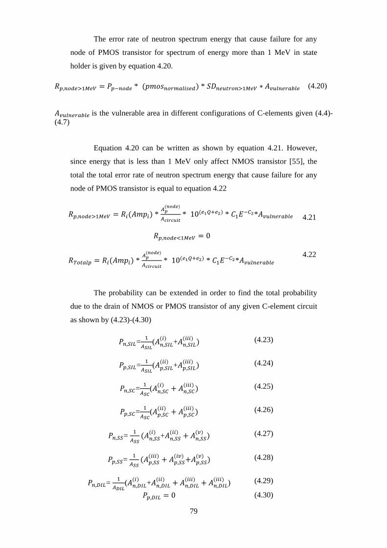
79
The error rate of neutron spectrum energy that cause failure for any
node of PMOS transistor for spectrum of energy more than 1 MeV in state
holder is given by equation 4.20.
𝑅𝑝,𝑛𝑜𝑑𝑒>1𝑀𝑒𝑉 = 𝑃𝑝−𝑛𝑜𝑑𝑒 * (𝑝𝑚𝑜𝑠𝑛𝑜𝑟𝑚𝑎𝑙𝑖𝑠𝑒𝑑) * 𝑆𝐷𝑛𝑒𝑢𝑡𝑟𝑜𝑛>1𝑀𝑒𝑉 ∗ 𝐴𝑣𝑢𝑙𝑛𝑒𝑟𝑎𝑏𝑙𝑒 (4.20)
𝐴𝑣𝑢𝑙𝑛𝑒𝑟𝑎𝑏𝑙𝑒 is the vulnerable area in different configurations of C-elements given (4.4)-
(4.7)
Equation 4.20 can be written as shown by equation 4.21. However,
since energy that is less than 1 MeV only affect NMOS transistor [55], the
total the total error rate of neutron spectrum energy that cause failure for any
node of PMOS transistor is equal to equation 4.22
𝑅𝑝,𝑛𝑜𝑑𝑒>1𝑀𝑒𝑉 = 𝑅𝑖(𝐴𝑚𝑝𝑖) * 𝐴𝑝(𝑛𝑜𝑑𝑒)
𝐴𝑐𝑖𝑟𝑐𝑢𝑖𝑡 * 10(𝑒1𝑄+𝑒2) * 𝐶1𝐸
−𝐶2*𝐴𝑣𝑢𝑙𝑛𝑒𝑟𝑎𝑏𝑙𝑒
4.21
𝑅𝑝,𝑛𝑜𝑑𝑒<1𝑀𝑒𝑉 = 0
𝑅𝑇𝑜𝑡𝑎𝑙𝑝 = 𝑅𝑖(𝐴𝑚𝑝𝑖) * 𝐴𝑝(𝑛𝑜𝑑𝑒)
𝐴𝑐𝑖𝑟𝑐𝑢𝑖𝑡 * 10(𝑒1𝑄+𝑒2) * 𝐶1𝐸
−𝐶2*𝐴𝑣𝑢𝑙𝑛𝑒𝑟𝑎𝑏𝑙𝑒 4.22
The probability can be extended in order to find the total probability
due to the drain of NMOS or PMOS transistor of any given C-element circuit
as shown by (4.23)-(4.30)
𝑃𝑛,𝑆𝐼𝐿=1
𝐴𝑆𝐼𝐿(𝐴𝑛,𝑆𝐼𝐿(𝑖)
+𝐴𝑛,𝑆𝐼𝐿(𝑖𝑖𝑖)
)
(4.23)
𝑃𝑝,𝑆𝐼𝐿=1
𝐴𝑆𝐼𝐿(𝐴𝑝,𝑆𝐼𝐿(𝑖𝑖)
+𝐴𝑝,𝑆𝐼𝐿(𝑖𝑖𝑖)
)
(4.24)
𝑃𝑛,𝑆𝐶=1
𝐴𝑆𝐶(𝐴𝑛,𝑆𝐶(𝑖)
+ 𝐴𝑛,𝑆𝐶(𝑖𝑖𝑖)
)
(4.25)
𝑃𝑝,𝑆𝐶=1
𝐴𝑆𝐶(𝐴𝑝,𝑆𝐶(𝑖𝑖)
+ 𝐴𝑝,𝑆𝐶(𝑖𝑖𝑖)
)
(4.26)
𝑃𝑛,𝑆𝑆= 1
𝐴𝑆𝑆(𝐴𝑛,𝑆𝑆
(𝑖)+𝐴𝑛,𝑆𝑆
(𝑖𝑖)+ 𝐴𝑛,𝑆𝑆
(𝑣))
(4.27)
𝑃𝑝,𝑆𝑆= 1
𝐴𝑆𝑆(𝐴𝑝,𝑆𝑆
(𝑖𝑖𝑖)+ 𝐴𝑝,𝑆𝑆
(𝑖𝑣)+𝐴𝑝,𝑆𝑆
(𝑣))
(4.28)
𝑃𝑛,𝐷𝐼𝐿= 1
𝐴𝐷𝐼𝐿(𝐴𝑛,𝐷𝐼𝐿(𝑖)
+𝐴𝑛,𝐷𝐼𝐿(𝑖𝑖)
+ 𝐴𝑛,𝐷𝐼𝐿(𝑖𝑖𝑖)
+ 𝐴𝑛,𝐷𝐼𝐿(𝑖𝑖𝑖)
) (4.29)
𝑃𝑝,𝐷𝐼𝐿 = 0 (4.30)

80
𝐴𝑆𝐼𝐿 , 𝐴𝑆𝐶 , 𝐴𝑆𝑆and 𝐴𝐷𝐼𝐿 are the total area of SIL, SC, SS and DIL respectively
The total probability of current pulse that hit for NMOS and PMOS
transistor in circuit are given by 4.31 and 4.32.
𝑃𝑛,𝑡𝑜𝑡𝑎𝑙= 𝑅𝑖(𝐴𝑚𝑝𝑖) * (𝑃𝑛,𝑐𝑖𝑟𝑐𝑢𝑖𝑡) (4.31)
𝑃𝑝,𝑡𝑜𝑡𝑎𝑙= 𝑅𝑖(𝐴𝑚𝑝𝑖) * (𝑃𝑝,𝑐𝑖𝑟𝑐𝑢𝑖𝑡) (4.32)
circuit= SIL,SC,SS or DIL
The total errors rate due to SEU of any configurations of C-elements
are given by 4.33-4.34
𝑅𝑇𝑜𝑡𝑎𝑙= Total error rate due to NMOS + Total error rate due to PMOS
(4.33)
𝑅𝑇𝑜𝑡𝑎𝑙 = 𝑃𝑛,𝑡𝑜𝑡𝑎𝑙 ∗ 10(𝑑1𝑄+𝑑2) ∗ 𝐶1𝐸
−𝐶2 ∗ 𝐴𝑐𝑖𝑟𝑐𝑢𝑖𝑡+𝑃𝑛,𝑡𝑜𝑡𝑎𝑙* 10(𝑑1𝑄+𝑑2)
∗ 3600 ∗ 10𝐶3𝐸−𝐶4*𝐴𝑐𝑖𝑟𝑐𝑢𝑖𝑡+𝑃𝑝,𝑡𝑜𝑡𝑎𝑙* 10(𝑒1𝑄+𝑒2) * 𝐶1𝐸−𝐶2*𝐴𝑐𝑖𝑟𝑐𝑢𝑖𝑡
(4.34)
4.3 Proposed Methods to Calculate Soft Error Rate
The methods are devised by using MATLAB to calculate the critical
charges based on the amplitude that generate 20% of the input and the
amplitude that cause the state to change for both NMOS and PMOS transistors
and to all the nodes. The normalised cross sections of NMOS and PMOS with
respect to neutron cross section are given by equations 4.12 and 4.13. The
code is given by Method 4.1.
Method 4.1 Calculate the critical charge and normalized cross section of NMOS/PMOS
with neutron
*Defining 𝑎1 = Amplitude of SEU that hit the drain of NMOS which generate pulse of
20% of the input
*Defining 𝑎2 = Amplitude of SEU that hit the drain of NMOS which cause state to
change
*Defining 𝑏1 = Amplitude of SEU that hit the drain of PMOS which generate pulse of
20% of the input
*Defining 𝑏2 = Amplitude of SEU that hit the drain of PMOS which cause state to change
*Calculate critical charge of NMOS = charge needed to change the current state
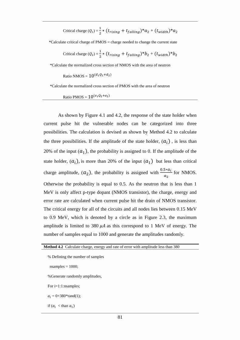
81
Critical charge (𝑄1) = 1
2∗ (𝑡𝑟𝑖𝑠𝑖𝑛𝑔 + 𝑡𝑓𝑎𝑙𝑙𝑖𝑛𝑔)*𝑎2 + (𝑡𝑤𝑖𝑑𝑡ℎ)*𝑎2
*Calculate critical charge of PMOS = charge needed to change the current state
Critical charge (𝑄2) = 1
2∗ (𝑡𝑟𝑖𝑠𝑖𝑛𝑔 + 𝑡𝑓𝑎𝑙𝑙𝑖𝑛𝑔)*𝑏2 + (𝑡𝑤𝑖𝑑𝑡ℎ)*𝑏2
*Calculate the normalized cross section of NMOS with the area of neutron
Ratio NMOS = 10(𝑑1𝑄1+𝑑2)
*Calculate the normalized cross section of PMOS with the area of neutron
Ratio PMOS = 10(𝑒1𝑄2+𝑒2)
As shown by Figure 4.1 and 4.2, the response of the state holder when
current pulse hit the vulnerable nodes can be categorized into three
possibilities. The calculation is devised as shown by Method 4.2 to calculate
the three possibilities. If the amplitude of the state holder, (𝑎𝑖) , is less than
20% of the input (𝑎1), the probability is assigned to 0. If the amplitude of the
state holder, (𝑎𝑖), is more than 20% of the input (𝑎1) but less than critical
charge amplitude, (𝑎2), the probability is assigned with 0.5∗𝑎𝑖
𝑎2 for NMOS.
Otherwise the probability is equal to 0.5. As the neutron that is less than 1
MeV is only affect p-type dopant (NMOS transistor), the charge, energy and
error rate are calculated when current pulse hit the drain of NMOS transistor.
The critical energy for all of the circuits and all nodes lies between 0.15 MeV
to 0.9 MeV, which is denoted by a circle as in Figure 2.3, the maximum
amplitude is limited to 380 𝜇𝐴 as this correspond to 1 MeV of energy. The
number of samples equal to 1000 and generate the amplitudes randomly.
Method 4.2 Calculate charge, energy and rate of error with amplitude less than 380
% Defining the number of samples
nsamples = 1000;
%Generate randomly amplitudes,
For i=1:1:nsamples;
𝑎𝑖 = 0+380*rand(1);
if (𝑎𝑖 < than 𝑎1)

82
Probability = 0;
Else if (𝑎1 ≤ 𝑎𝑖 < 𝑎2)
Probability = 0.5∗𝑎𝑖
𝑎2
Else
Probability = 0.5;
end;
if (𝑎1 ≤ 𝑎𝑖)
Charge less than 1 MeV (𝑄𝑛𝑜𝑑𝑒,𝑔𝑎𝑡𝑒) = 1
2∗ (𝑡𝑟𝑖𝑠𝑖𝑛𝑔 + 𝑡𝑓𝑎𝑙𝑙𝑖𝑛𝑔)* 𝑎𝑖 +
(𝑡𝑤𝑖𝑑𝑡ℎ)* 𝑎𝑖
Energy less than 1 MeV (E) = 3.6𝑒𝑉 𝑥 𝑄𝑛𝑜𝑑𝑒,𝑔𝑎𝑡𝑒
1.6𝑥10−19𝐶
Rate less than 1 MeV = 3600 ∗ 10(𝑐3∗𝐸−𝑐4) *Area of vulnerable*Ratio
NMOS
End
For energy of neutron that is more than 1 MeV, the amplitude from
380 𝜇𝐴 to 3620 𝜇𝐴 is generated randomly. This correspond to the neutron
energy equal to 1 MeV and 10 Mev of energy respectively, which is defined
by [56] as neutron environment at ground level. Method 4.3 is devised to
calculate the charge, energy and error rate when SEU hit the drain of NMOS
and PMOS transistor respectively. The differences of error rate between
PMOS and NMOS lies in the normalized cross section of PMOS and NMOS
and neutron cross section.
Method 4.3 Calculate charge, energy and rate of error with amplitude more than 380
% Defining the number of samples
nsamples = 1000;
%Generate randomly amplitudes for NMOS(𝑎𝑖) and PMOS(𝑏𝑖) respectively,
For i=1:1:nsamples;
𝑎𝑖= 380+3620*rand(1)
𝑏𝑖= 380+3620*rand(1)
*Calculate the charge, energy and error rate for NMOS with amplitude of SEU more than
380 𝜇𝐴

83
Charge more than 1 MeV (𝑄𝑛𝑜𝑑𝑒,𝑔𝑎𝑡𝑒) = 1
2∗ (𝑡𝑟𝑖𝑠𝑖𝑛𝑔 + 𝑡𝑓𝑎𝑙𝑙𝑖𝑛𝑔)* 𝑎𝑖 +
(𝑡𝑤𝑖𝑑𝑡ℎ)* 𝑎𝑖
Energy more than 1 MeV (E) = 3.6𝑒𝑉 𝑥 𝑄𝑛𝑜𝑑𝑒,𝑔𝑎𝑡𝑒
1.6𝑥10−19𝐶
Rate more than 1MeV = 𝑐1𝐸−𝑐2 * Area of vulnerable *Ratio NMOS
*Calculate the charge, energy and error rate for PMOS with amplitude of SEU more than
380 𝜇𝐴
Charge more than 1 MeV (𝑄𝑛𝑜𝑑𝑒,𝑔𝑎𝑡𝑒) = 1
2∗ (𝑡𝑟𝑖𝑠𝑖𝑛𝑔 + 𝑡𝑓𝑎𝑙𝑙𝑖𝑛𝑔)* 𝑏𝑖 +
(𝑡𝑤𝑖𝑑𝑡ℎ)* 𝑏𝑖
Energy more than 1 MeV (E) = 3.6𝑒𝑉 𝑥 𝑄𝑛𝑜𝑑𝑒,𝑔𝑎𝑡𝑒
1.6𝑥10−19𝐶
Rate more than 1 MeV = 𝑐1𝐸−𝑐2 * Area of vulnerable *Ratio PMOS
The error rates of current pulse hitting the drain of NMOS and PMOS
respectively are calculated for energy of neutron less than 1 MeV and more
than 1 MeV. For current that hit the drain of NMOS transistor, the error rate of
SEU less than 1 MeV and more than 1 MeV are added. But for the drain of
PMOS transistor, only the error rate of SEU for the neutron energy more than
1 MeV were taking into account as energy less than 1 Mev does not affect the
PMOS transistor. Method 4.4 is used to calculate the total error of SEU.
Method 4.4 Calculate error rate
*Calculate the probability of SEU event of the circuit with amplitude of SEU less than 380
𝜇𝐴
Probability of SEU (NMOS) = Probability*𝐴𝑟𝑒𝑎 𝑜𝑓 𝑑𝑟𝑎𝑖𝑛 𝑜𝑓 𝑁𝑀𝑂𝑆
𝑇𝑜𝑡𝑎𝑙 𝑎𝑟𝑒𝑎 𝑜𝑓 𝑐𝑖𝑟𝑐𝑢𝑖𝑡;
*Calculate the error rate of SEU
SEU Error Rate less than 1 MeV = Rate less than 1MeV* Probability of SEU (NMOS);
*Calculate the Sum of SEU Rate
Sum of SEU Rate less than 1 MeV =Sum(SEU Error Rate less than 1MeV);
*Calculate the probability of SEU event of the circuit with amplitude of SEU more than 380
𝜇𝐴
Probability of SEU (NMOS)= 0.5*𝐴𝑟𝑒𝑎 𝑜𝑓 𝑑𝑟𝑎𝑖𝑛 𝑜𝑓 𝑁𝑀𝑂𝑆
𝑇𝑜𝑡𝑎𝑙 𝑎𝑟𝑒𝑎 𝑜𝑓 𝑐𝑖𝑟𝑐𝑢𝑖𝑡;
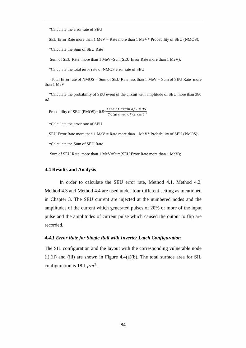
84
*Calculate the error rate of SEU
SEU Error Rate more than 1 MeV = Rate more than 1 MeV* Probability of SEU (NMOS);
*Calculate the Sum of SEU Rate
Sum of SEU Rate more than 1 MeV=Sum(SEU Error Rate more than 1 MeV);
*Calculate the total error rate of NMOS error rate of SEU
Total Error rate of NMOS = Sum of SEU Rate less than 1 MeV + Sum of SEU Rate more
than 1 MeV
*Calculate the probability of SEU event of the circuit with amplitude of SEU more than 380
𝜇𝐴
Probability of SEU (PMOS)= 0.5*𝐴𝑟𝑒𝑎 𝑜𝑓 𝑑𝑟𝑎𝑖𝑛 𝑜𝑓 𝑃𝑀𝑂𝑆
𝑇𝑜𝑡𝑎𝑙 𝑎𝑟𝑒𝑎 𝑜𝑓 𝑐𝑖𝑟𝑐𝑢𝑖𝑡;
*Calculate the error rate of SEU
SEU Error Rate more than 1 MeV = Rate more than 1 MeV* Probability of SEU (PMOS);
*Calculate the Sum of SEU Rate
Sum of SEU Rate more than 1 MeV=Sum(SEU Error Rate more than 1 MeV);
4.4 Results and Analysis
In order to calculate the SEU error rate, Method 4.1, Method 4.2,
Method 4.3 and Method 4.4 are used under four different setting as mentioned
in Chapter 3. The SEU current are injected at the numbered nodes and the
amplitudes of the current which generated pulses of 20% or more of the input
pulse and the amplitudes of current pulse which caused the output to flip are
recorded.
4.4.1 Error Rate for Single Rail with Inverter Latch Configuration
The SIL configuration and the layout with the corresponding vulnerable node
(i),(ii) and (iii) are shown in Figure 4.4(a)(b). The total surface area for SIL
configuration is 18.1 𝜇𝑚2.

85
Figure 4.4: (a) SIL Configuration Figure 4.4(b) : Layout SIL
Configuration [57]
The error rates as shown in Figure 4.5(a) of 0-1 change are higher
compared with error rate of 1-0 change by a factor of 4.09X at TT process
corner when A=1, B=0. Similarly, when A=0, B=1 the error rate of 0-1 change
are higher by a factor of 2.6X with the same process as shown by Figure
4.5(b). As expected, SS process corner has the highest error rate due to the
slowest transistors and FF process corner has the lowest rate due to the fastest
transistor for all nodes. In order to compare the relative error rate between the
process corners, the error rate for the same processes from Figure 4.5(a) and
(b) are added as shown in Figure 4.6(a) and (b). It is shown that the factor
variation between the extreme process corner (SS and FF) is 1.98X and 1.64X
when A=1,B=0 and A=0,B=1 respectively . The standard deviation of (TT,
SNFP and FNSP) is much smaller compared with the standard deviation of
(SS and FF) as shown by Table 4.1. The relatively small standard deviation
of TT, SNFP and FNSP indicates that the error rate between these process
corner are statistically identical compared with SS and FF.

86
No Process Corner Standard
Deviation (σ)
Percentage
difference w.r.t
(i)
A=1 B=0 SS,FF 5.61E-13 -
TT,SNFP,FNSP 1.18E-13 13.1%
SS,FF,TT,SNFP,FNSP 3.69E-13 64.7%
A=0 B=1 SS,FF 3.18E-12 -
TT,SNFP,FNSP 5E-14 1.6%
SS,FF,TT,SNFP,FNSP 2.02E-12 63.5%
Table 4.1 : Standard Deviation for the Process Corner-SIL
Figure 4.5(a): Error rate due to neutron energy spectrum with respect to
Process Corner SIL(A=1, B=0)
Figure 4.5(b): Error rate due to neutron energy spectrum with respect to
Process Corner SIL(A=0, B=1)
0.00E+00
1.00E-13
2.00E-13
3.00E-13
4.00E-13
5.00E-13
6.00E-13
7.00E-13
8.00E-13
9.00E-13
SIL ( Error Rate /hr) vs Process Corner
Out=0-1 Out=1-0
0.00E+00
1.00E-12
2.00E-12
3.00E-12
4.00E-12
5.00E-12
6.00E-12
7.00E-12
SIL ( Error Rate /hr) vs Process Corner
Out=0-1 Out=1-0
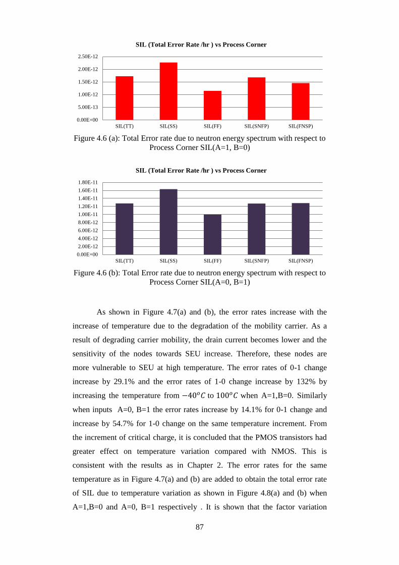
87
Figure 4.6 (a): Total Error rate due to neutron energy spectrum with respect to
Process Corner SIL(A=1, B=0)
Figure 4.6 (b): Total Error rate due to neutron energy spectrum with respect to
Process Corner SIL(A=0, B=1)
As shown in Figure 4.7(a) and (b), the error rates increase with the
increase of temperature due to the degradation of the mobility carrier. As a
result of degrading carrier mobility, the drain current becomes lower and the
sensitivity of the nodes towards SEU increase. Therefore, these nodes are
more vulnerable to SEU at high temperature. The error rates of 0-1 change
increase by 29.1% and the error rates of 1-0 change increase by 132% by
increasing the temperature from −40𝑜𝐶 to 100𝑜𝐶 when A=1,B=0. Similarly
when inputs A=0, B=1 the error rates increase by 14.1% for 0-1 change and
increase by 54.7% for 1-0 change on the same temperature increment. From
the increment of critical charge, it is concluded that the PMOS transistors had
greater effect on temperature variation compared with NMOS. This is
consistent with the results as in Chapter 2. The error rates for the same
temperature as in Figure 4.7(a) and (b) are added to obtain the total error rate
of SIL due to temperature variation as shown in Figure 4.8(a) and (b) when
A=1,B=0 and A=0, B=1 respectively . It is shown that the factor variation
0.00E+00
5.00E-13
1.00E-12
1.50E-12
2.00E-12
2.50E-12
SIL(TT) SIL(SS) SIL(FF) SIL(SNFP) SIL(FNSP)
SIL (Total Error Rate /hr ) vs Process Corner
0.00E+00
2.00E-12
4.00E-12
6.00E-12
8.00E-12
1.00E-11
1.20E-11
1.40E-11
1.60E-11
1.80E-11
SIL(TT) SIL(SS) SIL(FF) SIL(SNFP) SIL(FNSP)
SIL (Total Error Rate /hr ) vs Process Corner

88
between the extreme temperature variation are 1.46X and 1.23X and the
standard deviation due to the temperature variation is 2.4E-13 and 1E-13
respectively. This is smaller compared with standard deviation due to process
which is 3.69E-13 and 2.02E-13.We can conclude from the standard deviation
that temperature has lower effect on SEU compared with process corner.
Figure 4.7 (a): Error rate due to neutron energy spectrum with respect to
Temperature SIL (A=1 B=0)
Figure 4.7 (b): Error rate due to neutron energy spectrum with respect to
Temperature SIL (A=0, B=1)
Figure 4.8(a): Total Error rate due to neutron energy spectrum with respect to
Temperature-SIL(A=1, B=0)
0.00E+00
1.00E-13
2.00E-13
3.00E-13
4.00E-13
5.00E-13
6.00E-13
7.00E-13
8.00E-13
SIL (Error Rate /hr) vs Temperature
Out=0-1 Out=1-0
0.00E+00
1.00E-12
2.00E-12
3.00E-12
4.00E-12
5.00E-12
6.00E-12
SIL (Error Rate /hr) vs Temperature
Out=0-1 Out=1-0
0.00E+00
5.00E-13
1.00E-12
1.50E-12
2.00E-12
2.50E-12
SIL(-40C) SIL(0C) SIL(27C) SIL(100C)
SIL (Total Error Rate /hr) vs Temperature

89
Figure 4.8(b): Total Error rate due to neutron energy spectrum with respect to
Temperature-SIL(A=0, B=1)
From Figure 4.9(a), 4.10(a) and 4.11(a), it is observed that the error
rate between 0-1 change and 1-0 change decrease when the size is scaled. For
example, at nominal voltage of 1 V, the error rates between 0-1 change and 1-
0 change are 7.31X, 4.03X and 2.11X for the size of 150%, 100% and 50%
respectively when A=1, B=0. Similarly from Figure 4.9(b), 4.10(b) and
4.11(b), the error rates between 1-0 change and 0-1 change are 4.02X,2.77X
and 1.69X respectively when A=0, B=1. This indicates that as the size is
scaled, the resistance of PMOS transistors towards SEU decrease more than
NMOS transistors. As voltage supply is reduced, the error rate increases due to
the reduced in driving current causing the stored charged needed to flip the
output is also reduced. As a result the node is vulnerable to SEU when voltage
supply is reduced. The error rate with the same voltage are from Figure 4.9(a),
4.10(a) and 4.11(a) and Figure 4.9(b), 4.10(b) and 4.11(b) are added as shown
by Figure 4.12(a) and (b). When A=1,B=0 the soft error rate increases by a
factor 12.5X, 6.05X and 2.64X by scaling voltage from 1.2 V to 0.8 V for
150%, 100% and 50% of nominal size respectively. Similarly when A=0,B=1
the soft error rate increases by a factor 4.64X, 2.99X and 1.77X by scaling
voltage from 1.2 V to 0.8 V for 150%, 100% and 50% of nominal size
respectively. Compared with process corner variation and temperature, voltage
scaling has the highest impact on the rate of SEU error. Generally, as the size
increases, the critical charge needed to change the state is increased. By
increasing the width of the transistor, the output node capacitance is also
increased and therefore the charge needed to change the state is also increased.
In other words, the smaller is the size, the circuit is more vulnerable to SEU.
0.00E+00
2.00E-12
4.00E-12
6.00E-12
8.00E-12
1.00E-11
1.20E-11
1.40E-11
1.60E-11
SIL(-40C) SIL(0C) SIL(27C) SIL(100C)
SIL (Total Error Rate /hr) vs Temperature

90
However, as the size of circuit is decreased, the probability of hitting by
current pulse is also smaller. For error rate, there is a trade-off between the
size of the circuit and the probability of hitting by SEU.
Figure 4.9(a): Error rate due to neutron energy spectrum with respect to
Voltage Supply for 50% SIL (A=1, B=0)
Figure 4.9(b): Error rate due to neutron energy spectrum with respect to
Voltage Supply for 50% SIL (A=0, B=1)
Figure 4.10(a): Error rate due to neutron energy spectrum with respect to
Voltage Supply for 100% SIL (A=1, B=0)
0.00E+00
2.00E-13
4.00E-13
6.00E-13
8.00E-13
1.00E-12
1.20E-12
1.40E-12
1.60E-12
1.80E-12
SIL (Error Rate /hr) for 50% of Nominal Sizing
Out=0-1 Out=1-0
0.00E+00
1.00E-12
2.00E-12
3.00E-12
4.00E-12
5.00E-12
6.00E-12
SIL (Error Rate /hr) for 50% of Nominal Sizing
Out=0-1 Out=1-0
0.00E+00
2.00E-13
4.00E-13
6.00E-13
8.00E-13
1.00E-12
1.20E-12
1.40E-12
1.60E-12
SIL (Error Rate /hr) for 100% of Nominal Sizing
Out=0-1 Out=1-0

91
Figure 4.10(b): Error rate due to neutron energy spectrum with respect to
Voltage Supply for 100% SIL (A=0, B=1)
Figure 4.11(a): Error rate due to neutron energy spectrum with respect to
Voltage Supply for 150% SIL (A=1, B=0)
Figure 4.11(b): Error rate due to neutron energy spectrum with respect to
Voltage Supply for 150% SIL (A=0, B=1)
0.00E+00
1.00E-12
2.00E-12
3.00E-12
4.00E-12
5.00E-12
6.00E-12
7.00E-12
8.00E-12
SIL (Error Rate /hr) for 100% of Nominal Sizing
Out=0-1 Out=1-0
0.00E+00
1.00E-13
2.00E-13
3.00E-13
4.00E-13
5.00E-13
6.00E-13
SIL (Error Rate /hr) for 150% of Nominal Sizing
Out=0-1 Out=1-0
0.00E+00
1.00E-12
2.00E-12
3.00E-12
4.00E-12
5.00E-12
6.00E-12
7.00E-12
8.00E-12
SIL (Error Rate /hr) for 150% of Nominal Sizing
Out=0-1 Out=1-0

92
Figure 4.12(a): Total error rate due to neutron energy spectrum with respect to
Voltage Supply for SIL (A=1, B=0)
Figure 4.12(b): Total error rate due to neutron energy spectrum with respect
to Voltage Supply for SIL (A=0, B=1)
Sensitivity Analysis for SIL configuration
In chapter 3, the nodes sensitivity are obtained by calculating the
standard deviation of the critical charge on every node in C-elements. In this
chapter, the nodes sensitivity are obtained by calculating the standard
deviation of the error rate on every nodes to obtain the correct representation
of the variation of the critical charges towards process corner, temperature,
voltage and size scaling as shown by Figure 4.13 (a) and (b). Voltage scaling
has the highest value of standard deviation which suggests that the error rates
are very sensitive to the change in the voltage supply. Standard deviation for
the process is significant than size for inputs A=0,B=1 which suggests that the
0.00E+00
1.00E-12
2.00E-12
3.00E-12
4.00E-12
5.00E-12
6.00E-12
Total Error Rate (/hr) of Different Sizing SIL
0.00E+00
5.00E-12
1.00E-11
1.50E-11
2.00E-11
2.50E-11
Total Error Rate (/hr) of Different Sizing SIL
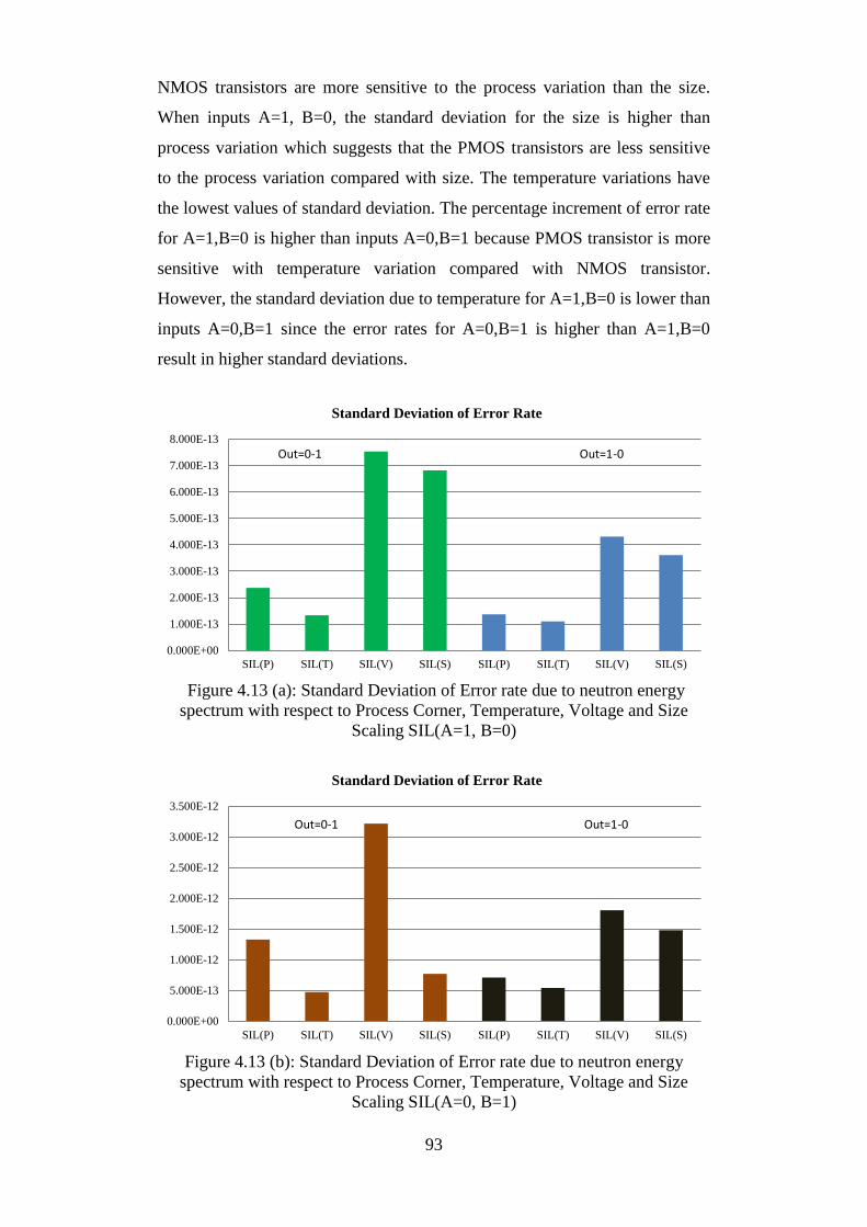
93
NMOS transistors are more sensitive to the process variation than the size.
When inputs A=1, B=0, the standard deviation for the size is higher than
process variation which suggests that the PMOS transistors are less sensitive
to the process variation compared with size. The temperature variations have
the lowest values of standard deviation. The percentage increment of error rate
for A=1,B=0 is higher than inputs A=0,B=1 because PMOS transistor is more
sensitive with temperature variation compared with NMOS transistor.
However, the standard deviation due to temperature for A=1,B=0 is lower than
inputs A=0,B=1 since the error rates for A=0,B=1 is higher than A=1,B=0
result in higher standard deviations.
Figure 4.13 (a): Standard Deviation of Error rate due to neutron energy
spectrum with respect to Process Corner, Temperature, Voltage and Size
Scaling SIL(A=1, B=0)
Figure 4.13 (b): Standard Deviation of Error rate due to neutron energy
spectrum with respect to Process Corner, Temperature, Voltage and Size
Scaling SIL(A=0, B=1)
0.000E+00
1.000E-13
2.000E-13
3.000E-13
4.000E-13
5.000E-13
6.000E-13
7.000E-13
8.000E-13
SIL(P) SIL(T) SIL(V) SIL(S) SIL(P) SIL(T) SIL(V) SIL(S)
Standard Deviation of Error Rate
Out=0-1 Out=1-0
0.000E+00
5.000E-13
1.000E-12
1.500E-12
2.000E-12
2.500E-12
3.000E-12
3.500E-12
SIL(P) SIL(T) SIL(V) SIL(S) SIL(P) SIL(T) SIL(V) SIL(S)
Standard Deviation of Error Rate
Out=0-1 Out=1-0
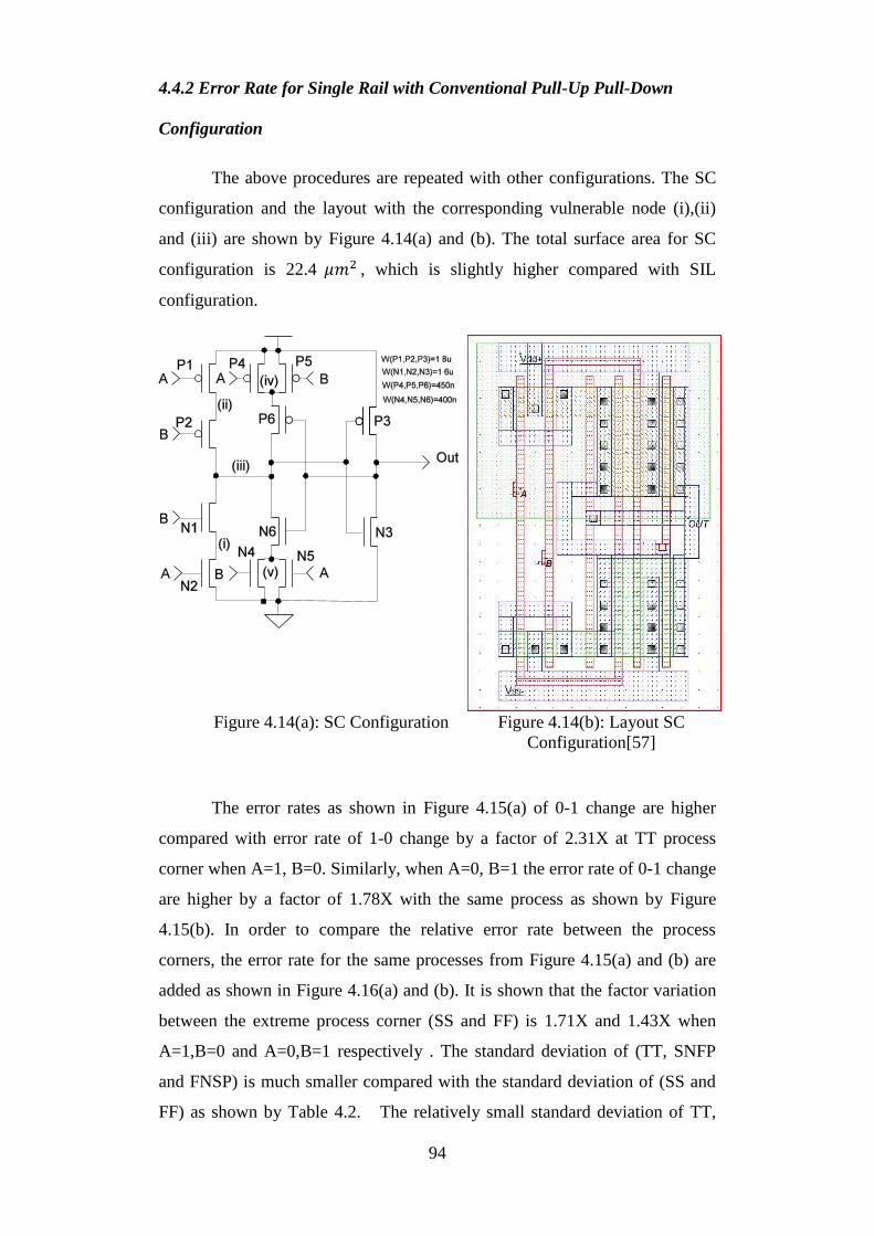
94
4.4.2 Error Rate for Single Rail with Conventional Pull-Up Pull-Down
Configuration
The above procedures are repeated with other configurations. The SC
configuration and the layout with the corresponding vulnerable node (i),(ii)
and (iii) are shown by Figure 4.14(a) and (b). The total surface area for SC
configuration is 22.4 𝜇𝑚2 , which is slightly higher compared with SIL
configuration.
Figure 4.14(a): SC Configuration Figure 4.14(b): Layout SC
Configuration[57]
The error rates as shown in Figure 4.15(a) of 0-1 change are higher
compared with error rate of 1-0 change by a factor of 2.31X at TT process
corner when A=1, B=0. Similarly, when A=0, B=1 the error rate of 0-1 change
are higher by a factor of 1.78X with the same process as shown by Figure
4.15(b). In order to compare the relative error rate between the process
corners, the error rate for the same processes from Figure 4.15(a) and (b) are
added as shown in Figure 4.16(a) and (b). It is shown that the factor variation
between the extreme process corner (SS and FF) is 1.71X and 1.43X when
A=1,B=0 and A=0,B=1 respectively . The standard deviation of (TT, SNFP
and FNSP) is much smaller compared with the standard deviation of (SS and
FF) as shown by Table 4.2. The relatively small standard deviation of TT,
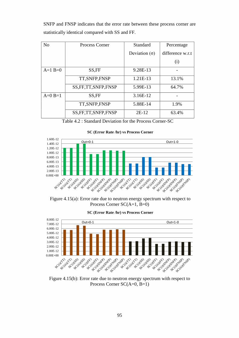
95
SNFP and FNSP indicates that the error rate between these process corner are
statistically identical compared with SS and FF.
No Process Corner Standard
Deviation (σ)
Percentage
difference w.r.t
(i)
A=1 B=0 SS,FF 9.28E-13 -
TT,SNFP,FNSP 1.21E-13 13.1%
SS,FF,TT,SNFP,FNSP 5.99E-13 64.7%
A=0 B=1 SS,FF 3.16E-12 -
TT,SNFP,FNSP 5.88E-14 1.9%
SS,FF,TT,SNFP,FNSP 2E-12 63.4%
Table 4.2 : Standard Deviation for the Process Corner-SC
Figure 4.15(a): Error rate due to neutron energy spectrum with respect to
Process Corner SC(A=1, B=0)
Figure 4.15(b): Error rate due to neutron energy spectrum with respect to
Process Corner SC(A=0, B=1)
0.00E+00
2.00E-13
4.00E-13
6.00E-13
8.00E-13
1.00E-12
1.20E-12
1.40E-12
1.60E-12
SC (Error Rate /hr) vs Process Corner
Out=0-1 Out=1-0
0.00E+00
1.00E-12
2.00E-12
3.00E-12
4.00E-12
5.00E-12
6.00E-12
7.00E-12
8.00E-12
SC (Error Rate /hr) vs Process Corner
Out=0-1 Out=1-0

96
Figure 4.16(a): Total Error rate due to neutron energy spectrum with respect to
Process Corner SC(A=1, B=0)
Figure 4.16(b): Total Error rate due to neutron energy spectrum with respect
to Process Corner SC(A=0, B=1)
The error rates of 0-1 change increase by 14.2% and the error rates of
1-0 change increase by 73.9% by increasing the temperature from −40𝑜𝐶 to
100𝑜𝐶 when A=1,B=0 as shown by Figure 4.17(a). Similarly when inputs
A=0, B=1 the error rates increase by 6.3% for 0-1 change and increase by
30.3% for 1-0 change on the same temperature increment as shown by Figure
4.17(b). The error rates for the same temperature as in Figure 4.17(a) and (b)
are added to obtain the total error rate of SC due to temperature variation as
shown in Figure 4.18(a) and (b) when A=1,B=0 and A=0, B=1 respectively . It
is shown that the factor variation between the extreme temperature variations
are 1.29X and 1.14X and the standard deviation due to the temperature
variation is 3.29E-13 and 8.66E-13 respectively. This is smaller compared
with standard deviation due to process which is 5.99E-13 and 2E-12
respectively. We can conclude from the standard deviation that temperature
has lower effect on SEU compared with process corner
0.00E+00
1.00E-12
2.00E-12
3.00E-12
4.00E-12
5.00E-12
SC(TT) SC(SS) SC(FF) SC(SNFP) SC(FNSP)
SC (Total Error Rate /hr) vs Process Corner
0.00E+00
5.00E-12
1.00E-11
1.50E-11
2.00E-11
2.50E-11
SC(TT) SC(SS) SC(FF) SC(SNFP) SC(FNSP)
SC (Total Error Rate /hr) vs Process Corner
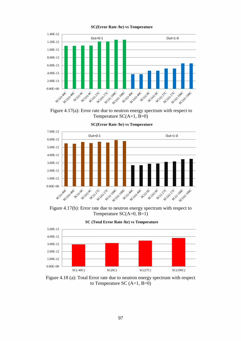
97
Figure 4.17(a): Error rate due to neutron energy spectrum with respect to
Temperature SC(A=1, B=0)
Figure 4.17(b): Error rate due to neutron energy spectrum with respect to
Temperature SC(A=0, B=1)
Figure 4.18 (a): Total Error rate due to neutron energy spectrum with respect
to Temperature SC (A=1, B=0)
0.00E+00
2.00E-13
4.00E-13
6.00E-13
8.00E-13
1.00E-12
1.20E-12
1.40E-12
SC(Error Rate /hr) vs Temperature
Out=0-1 Out=1-0
0.00E+00
1.00E-12
2.00E-12
3.00E-12
4.00E-12
5.00E-12
6.00E-12
7.00E-12
SC(Error Rate /hr) vs Temperature
Out=0-1 Out=1-0
0.00E+00
1.00E-12
2.00E-12
3.00E-12
4.00E-12
5.00E-12
SC(-40C) SC(0C) SC(27C) SC(100C)
SC (Total Error Rate /hr) vs Temperature

98
Figure 4.18 (b): Total Error rate due to neutron energy spectrum with respect
to Temperature SC (A=0, B=1)
From Figure 4.19(a), 4.20(a) and 4.21(a), it is observed that the error
rate between 0-1 change and 1-0 change decrease when the size is scaled. For
example, at nominal voltage of 1 V, the error rates between 0-1 change and 1-
0 change are 2.89X, 2.47X and 1.50X for the size of 150%, 100% and 50%
respectively when A=1, B=0. Similarly from Figure 4.19(b), 4.20(b) and
4.21(b), the error rates between 1-0 change and 0-1 change are 2.50X,1.76X
and 1.51X when A=0, B=1. The error rates with the same voltage are added
as shown by Figure 4.22(a) and (b) for A=1,B=0 and A=0,B=1 respectively.
The soft error rate increases by a factor 6.03X, 3.63X and 2.06X by scaling
voltage from 1.2 V to 0.8 V for 150%, 100% and 50% of nominal size
respectively for A=1,B=0 . Similarly, when A=0,B=1 the soft error rate
increases by a factor 2.89X, 2.06X and 1.51X by scaling voltage from 1.2 V to
0.8 V for 150%, 100% and 50% of nominal size respectively A=0,B=1.
Figure 4.19(a): Error rate due to neutron energy spectrum with respect to
Voltage Supply for 50% SC (A=1, B=0)
0.00E+00
5.00E-12
1.00E-11
1.50E-11
2.00E-11
SC(-40C) SC(0C) SC(27C) SC(100C)
SC (Total Error Rate /hr) vs Temperature
0.00E+00
2.00E-13
4.00E-13
6.00E-13
8.00E-13
1.00E-12
1.20E-12
1.40E-12
1.60E-12
1.80E-12
2.00E-12
SC (Error Rate /hr) for 50% of Nominal Sizing
Out=0-1 Out=1-0

99
Figure 4.19(b): Error rate due to neutron energy spectrum with respect to
Voltage Supply for 50% SC (A=0, B=1)
Figure 4.20(a): Error rate due to neutron energy spectrum with respect to
Voltage Supply for 100% SC (A=1, B=0)
Figure 4.20(b): Error rate due to neutron energy spectrum with respect to
Voltage Supply for 100% SC (A=0, B=1)
0.00E+00
1.00E-12
2.00E-12
3.00E-12
4.00E-12
5.00E-12
6.00E-12
SC (Error Rate /hr) for 50% of Nominal Sizing
Out=0-1 Out=1-0
0.00E+00
5.00E-13
1.00E-12
1.50E-12
2.00E-12
2.50E-12
SC (Error Rate /hr) for 100% of Nominal Sizing
Out=0-1 Out=1-0
0.00E+00
1.00E-12
2.00E-12
3.00E-12
4.00E-12
5.00E-12
6.00E-12
7.00E-12
8.00E-12
9.00E-12
SC (Error Rate /hr) for 100% of Nominal Sizing
Out=0-1 Out=1-0

100
Figure 4.21(a): Error rate due to neutron energy spectrum with respect to
Voltage Supply for 150% SC (A=1, B=0)
Figure 4.21(b): Error rate due to neutron energy spectrum with respect to
Voltage Supply for 150% SC (A=0, B=1)
Figure 4.22(a): Total error rate due to neutron energy spectrum with respect to
0.00E+00
2.00E-13
4.00E-13
6.00E-13
8.00E-13
1.00E-12
1.20E-12
1.40E-12
1.60E-12
SC(Error Rate /hr) for 150% of Nominal Sizing
Out=0-1 Out=1-0
0.00E+00
1.00E-12
2.00E-12
3.00E-12
4.00E-12
5.00E-12
6.00E-12
7.00E-12
8.00E-12
9.00E-12
SC(Error Rate /hr) for 150% of Nominal Sizing
Out=0-1 Out=1-0
0.00E+00
1.00E-12
2.00E-12
3.00E-12
4.00E-12
5.00E-12
6.00E-12
7.00E-12
Total Error Rate (/hr) of Different Sizing SC

101
Voltage Supply for SC (A=1, B=0)
Figure 4.22(b): Total error rate due to neutron energy spectrum with respect to
Voltage Supply for SC (A=0, B=1)
Sensitivity Analysis for SC configuration
The nodes sensitivity are obtained by calculating the standard
deviation of the error rate on every nodes to obtain the correct representation
of the variation of the critical charges towards process corner, temperature,
voltage and size scaling as shown by Figure 4.23 (a) and (b). As for SIL,
voltage scaling has the highest value of standard deviation which suggests that
the error rates are very sensitive to the change in the voltage supply. Standard
deviation for the process is significant than size for inputs A=0,B=1 which
suggests that the NMOS transistors are more sensitive to the process variation
than the size. When inputs A=1, B=0, the standard deviation for the size is
higher than process variation which suggests that the PMOS transistors are
less sensitive to the process variation compared with size. The temperature
variations have the lowest values of standard deviation. As for SIL, the
percentage increment of error rate for A=1,B=0 is higher than inputs A=0,B=1
because PMOS transistor is more sensitive with temperature variation
compared with NMOS transistor. However, the standard deviation due to
temperature for A=1,B=0 is lower than inputs A=0,B=1 since the error rates
for A=0,B=1 is higher than A=1,B=0 result in higher standard deviations.
0.00E+00
5.00E-12
1.00E-11
1.50E-11
2.00E-11
2.50E-11
3.00E-11
Total Error Rate (/hr) of Different Sizing SC
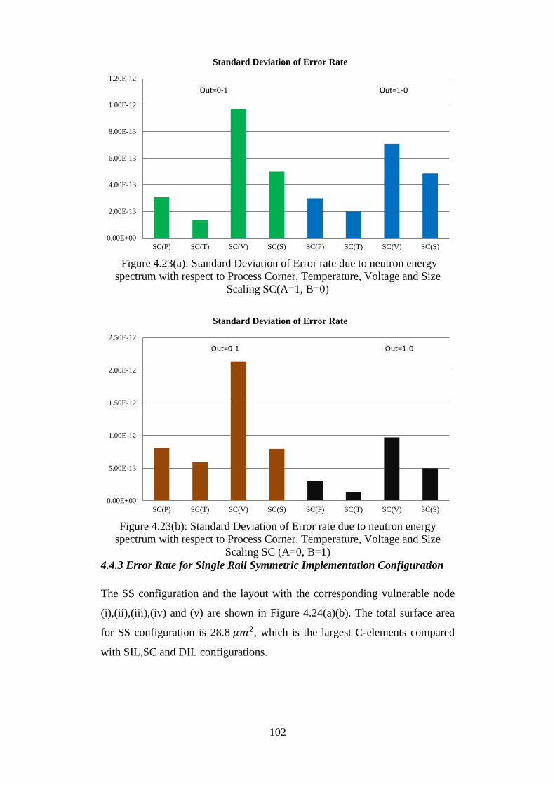
102
Figure 4.23(a): Standard Deviation of Error rate due to neutron energy
spectrum with respect to Process Corner, Temperature, Voltage and Size
Scaling SC(A=1, B=0)
Figure 4.23(b): Standard Deviation of Error rate due to neutron energy
spectrum with respect to Process Corner, Temperature, Voltage and Size
Scaling SC (A=0, B=1)
4.4.3 Error Rate for Single Rail Symmetric Implementation Configuration
The SS configuration and the layout with the corresponding vulnerable node
(i),(ii),(iii),(iv) and (v) are shown in Figure 4.24(a)(b). The total surface area
for SS configuration is 28.8 𝜇𝑚2, which is the largest C-elements compared
with SIL,SC and DIL configurations.
0.00E+00
2.00E-13
4.00E-13
6.00E-13
8.00E-13
1.00E-12
1.20E-12
SC(P) SC(T) SC(V) SC(S) SC(P) SC(T) SC(V) SC(S)
Standard Deviation of Error Rate
Out=0-1 Out=1-0
0.00E+00
5.00E-13
1.00E-12
1.50E-12
2.00E-12
2.50E-12
SC(P) SC(T) SC(V) SC(S) SC(P) SC(T) SC(V) SC(S)
Standard Deviation of Error Rate
Out=0-1 Out=1-0

103
Figure 4.24(a): SS
configuration
Figure 4.24(b): Layout SS
Configuration[57]
For SS configuration, injecting current pulse at node (ii),(iii) and (v)
cause 0-1 change and 1-0 change when A=1, B=0 and node (i),(iv) and (v)
when A=0,B=1. The error rates as shown in Figure 4.25(a) of 0-1 change are
higher compared with error rate of 1-0 change by a factor of 3.31X at TT
process corner when A=1, B=0. Similarly when A=0, B=1 the error rate of are
higher by a factor of 2.77X with the same process as shown by Figure 4.25(b).
In order to compare the relative error rate between the process corners, the
error rate for all the processes from Figure 4.25(a) and (b) are added as shown
in Figure 4.26(a) and (b). It is shown that the factor variation between the
extreme process corner (SS and FF) is 1.91X and 1.76X when A=1,B=0 and
A=0,B=1 respectively . The standard deviation of (TT, SNFP and FNSP) is
much smaller compared with the standard deviation of (SS and FF) as shown
by Table 4.3. The relatively small standard deviation of TT, SNFP and FNSP
indicates that the error rate between these process corner are statistically
identical compared with SS and FF.
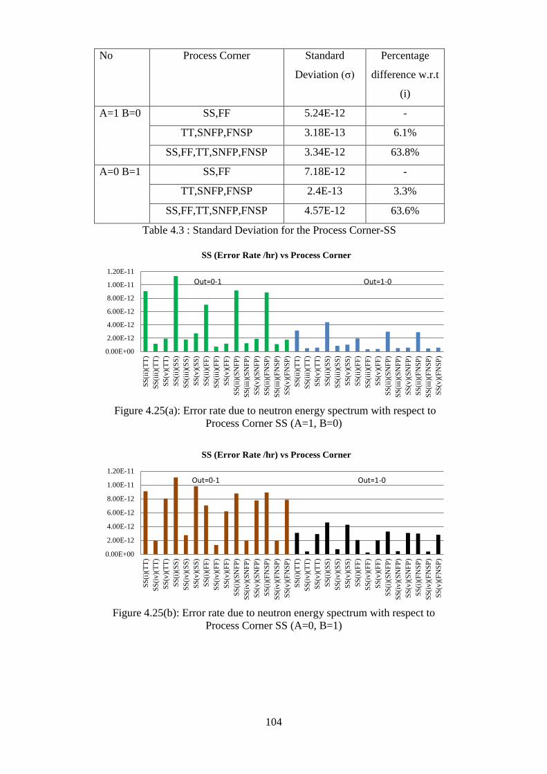
104
No Process Corner Standard
Deviation (σ)
Percentage
difference w.r.t
(i)
A=1 B=0 SS,FF 5.24E-12 -
TT,SNFP,FNSP 3.18E-13 6.1%
SS,FF,TT,SNFP,FNSP 3.34E-12 63.8%
A=0 B=1 SS,FF 7.18E-12 -
TT,SNFP,FNSP 2.4E-13 3.3%
SS,FF,TT,SNFP,FNSP 4.57E-12 63.6%
Table 4.3 : Standard Deviation for the Process Corner-SS
Figure 4.25(a): Error rate due to neutron energy spectrum with respect to
Process Corner SS (A=1, B=0)
Figure 4.25(b): Error rate due to neutron energy spectrum with respect to
Process Corner SS (A=0, B=1)
0.00E+00
2.00E-12
4.00E-12
6.00E-12
8.00E-12
1.00E-11
1.20E-11
SS
(ii)
(TT
)
SS
(iii
)(T
T)
SS
(v)(
TT
)
SS
(ii)
(SS
)
SS
(iii
)(S
S)
SS
(v)(
SS
)
SS
(ii)
(FF
)
SS
(iii
)(F
F)
SS
(v)(
FF
)
SS
(ii)
(SN
FP
)
SS
(iii
)(S
NF
P)
SS
(v)(
SN
FP
)
SS
(ii)
(FN
SP
)
SS
(iii
)(F
NS
P)
SS
(v)(
FN
SP
)
SS
(ii)
(TT
)
SS
(iii
)(T
T)
SS
(v)(
TT
)
SS
(ii)
(SS
)
SS
(iii
)(S
S)
SS
(v)(
SS
)
SS
(ii)
(FF
)
SS
(iii
)(F
F)
SS
(v)(
FF
)
SS
(ii)
(SN
FP
)
SS
(iii
)(S
NF
P)
SS
(v)(
SN
FP
)
SS
(ii)
(FN
SP
)
SS
(iii
)(F
NS
P)
SS
(v)(
FN
SP
)
SS (Error Rate /hr) vs Process Corner
Out=0-1 Out=1-0
0.00E+00
2.00E-12
4.00E-12
6.00E-12
8.00E-12
1.00E-11
1.20E-11
SS
(i)(
TT
)
SS
(iv)(
TT
)
SS
(v)(
TT
)
SS
(i)(
SS
)
SS
(iv)(
SS
)
SS
(v)(
SS
)
SS
(i)(
FF
)
SS
(iv)(
FF
)
SS
(v)(
FF
)
SS
(i)(
SN
FP
)
SS
(iv)(
SN
FP
)
SS
(v)(
SN
FP
)
SS
(i)(
FN
SP
)
SS
(iv)(
FN
SP
)
SS
(v)(
FN
SP
)
SS
(i)(
TT
)
SS
(iv)(
TT
)
SS
(v)(
TT
)
SS
(i)(
SS
)
SS
(iv)(
SS
)
SS
(v)(
SS
)
SS
(i)(
FF
)
SS
(iv)(
FF
)
SS
(v)(
FF
)
SS
(i)(
SN
FP
)
SS
(iv)(
SN
FP
)
SS
(v)(
SN
FP
)
SS
(i)(
FN
SP
)
SS
(iv)(
FN
SP
)
SS
(v)(
FN
SP
)
SS (Error Rate /hr) vs Process Corner
Out=0-1 Out=1-0
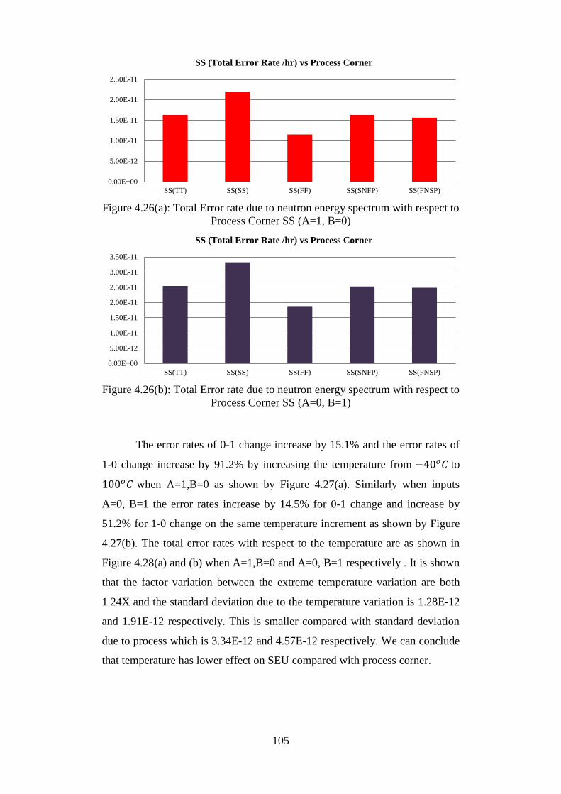
105
Figure 4.26(a): Total Error rate due to neutron energy spectrum with respect to
Process Corner SS (A=1, B=0)
Figure 4.26(b): Total Error rate due to neutron energy spectrum with respect to
Process Corner SS (A=0, B=1)
The error rates of 0-1 change increase by 15.1% and the error rates of
1-0 change increase by 91.2% by increasing the temperature from −40𝑜𝐶 to
100𝑜𝐶 when A=1,B=0 as shown by Figure 4.27(a). Similarly when inputs
A=0, B=1 the error rates increase by 14.5% for 0-1 change and increase by
51.2% for 1-0 change on the same temperature increment as shown by Figure
4.27(b). The total error rates with respect to the temperature are as shown in
Figure 4.28(a) and (b) when A=1,B=0 and A=0, B=1 respectively . It is shown
that the factor variation between the extreme temperature variation are both
1.24X and the standard deviation due to the temperature variation is 1.28E-12
and 1.91E-12 respectively. This is smaller compared with standard deviation
due to process which is 3.34E-12 and 4.57E-12 respectively. We can conclude
that temperature has lower effect on SEU compared with process corner.
0.00E+00
5.00E-12
1.00E-11
1.50E-11
2.00E-11
2.50E-11
SS(TT) SS(SS) SS(FF) SS(SNFP) SS(FNSP)
SS (Total Error Rate /hr) vs Process Corner
0.00E+00
5.00E-12
1.00E-11
1.50E-11
2.00E-11
2.50E-11
3.00E-11
3.50E-11
SS(TT) SS(SS) SS(FF) SS(SNFP) SS(FNSP)
SS (Total Error Rate /hr) vs Process Corner

106
Figure 4.27(a): Error rate due to neutron energy spectrum with respect to
Temperature SS (A=1, B=0)
Figure 4.27(b): Error rate due to neutron energy spectrum with respect to
Temperature SS (A=0, B=1)
Figure 4.28(a): Total Error rate due to neutron energy spectrum with respect to
Temperature SS (A=1, B=0)
0.00E+00
1.00E-12
2.00E-12
3.00E-12
4.00E-12
5.00E-12
6.00E-12
7.00E-12
8.00E-12
9.00E-12
1.00E-11
SS (Error Rate /hr) vs Temperature
Out=0-1 Out=1-0
0.00E+00
1.00E-12
2.00E-12
3.00E-12
4.00E-12
5.00E-12
6.00E-12
7.00E-12
8.00E-12
9.00E-12
1.00E-11
SS (Error Rate /hr) vs Temperature
Out=0-1 Out=1-0
0.00E+00
5.00E-12
1.00E-11
1.50E-11
2.00E-11
SS(-40C) SS(0C) SS(27C) SS(100C)
SS (Total Error Rate /hr) vs Temperature
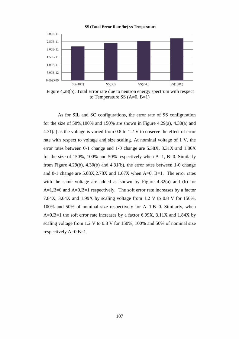
107
Figure 4.28(b): Total Error rate due to neutron energy spectrum with respect
to Temperature SS (A=0, B=1)
As for SIL and SC configurations, the error rate of SS configuration
for the size of 50%,100% and 150% are shown in Figure 4.29(a), 4.30(a) and
4.31(a) as the voltage is varied from 0.8 to 1.2 V to observe the effect of error
rate with respect to voltage and size scaling. At nominal voltage of 1 V, the
error rates between 0-1 change and 1-0 change are 5.38X, 3.31X and 1.86X
for the size of 150%, 100% and 50% respectively when A=1, B=0. Similarly
from Figure 4.29(b), 4.30(b) and 4.31(b), the error rates between 1-0 change
and 0-1 change are 5.08X,2.78X and 1.67X when A=0, B=1. The error rates
with the same voltage are added as shown by Figure 4.32(a) and (b) for
A=1,B=0 and A=0,B=1 respectively. The soft error rate increases by a factor
7.84X, 3.64X and 1.99X by scaling voltage from 1.2 V to 0.8 V for 150%,
100% and 50% of nominal size respectively for A=1,B=0. Similarly, when
A=0,B=1 the soft error rate increases by a factor 6.99X, 3.11X and 1.84X by
scaling voltage from 1.2 V to 0.8 V for 150%, 100% and 50% of nominal size
respectively A=0,B=1.
0.00E+00
5.00E-12
1.00E-11
1.50E-11
2.00E-11
2.50E-11
3.00E-11
SS(-40C) SS(0C) SS(27C) SS(100C)
SS (Total Error Rate /hr) vs Temperature

108
Figure 4.29(a): Error rate due to neutron energy spectrum with respect to
Voltage Supply for 50% SS (A=1, B=0)
Figure 4.29(b): Error rate due to neutron energy spectrum with respect to
Voltage Supply for 50% SS (A=0, B=1)
Figure 4.30(a): Error rate due to neutron energy spectrum with respect to
Voltage Supply for 100% SS (A=1, B=0)
0.00E+00
2.00E-12
4.00E-12
6.00E-12
8.00E-12
1.00E-11
1.20E-11
SS
(ii)
0.8
V
SS
(iii
)0.8
V
SS
(v)0
.8V
SS
(ii)
0.9
V
SS
(iii
)0.9
V
SS
(v)0
.9V
SS
(ii)
1V
SS
(iii
)1V
SS
(v)1
V
SS
(ii)
1.1
V
SS
(iii
)1.1
V
SS
(v)1
.1V
SS
(ii)
1.2
V
SS
(iii
)1.2
V
SS
(v)1
.2V
SS
(ii)
0.8
V
SS
(iii
)0.8
V
SS
(v)0
.8V
SS
(ii)
0.9
V
SS
(iii
)0.9
V
SS
(v)0
.9V
SS
(ii)
1V
SS
(iii
)1V
SS
(v)1
V
SS
(ii)
1.1
V
SS
(iii
)1.1
V
SS
(v)1
.1V
SS
(ii)
1.2
V
SS
(iii
)1.2
V
SS
(v)1
.2V
SS (Error Rate /hr) for 50% 0f Nominal Sizing
Out=0-1 Out=1-0
0.00E+00
2.00E-12
4.00E-12
6.00E-12
8.00E-12
1.00E-11
1.20E-11
SS
(i)0
.8V
SS
(iv)0
.8V
SS
(v)0
.8V
SS
(i)0
.9V
SS
(iv)0
.9V
SS
(v)0
.9V
SS
(i)1
V
SS
(iv)1
V
SS
(v)1
V
SS
(i)1
.1V
SS
(iv)1
.1V
SS
(v)1
.1V
SS
(i)1
.2V
SS
(iv)1
.2V
SS
(v)1
.2V
SS
(i)0
.8V
SS
(iv)0
.8V
SS
(v)0
.8V
SS
(i)0
.9V
SS
(iv)0
.9V
SS
(v)0
.9V
SS
(i)1
V
SS
(iv)1
V
SS
(v)1
V
SS
(i)1
.1V
SS
(iv)1
.1V
SS
(v)1
.1V
SS
(i)1
.2V
SS
(iv)1
.2V
SS
(v)1
.2V
SS (Error Rate /hr) for 50% 0f Nominal Sizing
Out=0-1 Out=1-0
0.00E+00
2.00E-12
4.00E-12
6.00E-12
8.00E-12
1.00E-11
1.20E-11
1.40E-11
1.60E-11
SS
(ii)
0.8
V
SS
(iii
)0.8
V
SS
(v)0
.8V
SS
(ii)
0.9
V
SS
(iii
)0.9
V
SS
(v)0
.9V
SS
(ii)
1V
SS
(iii
)1V
SS
(v)1
V
SS
(ii)
1.1
V
SS
(iii
)1.1
V
SS
(v)1
.1V
SS
(ii)
1.2
V
SS
(iii
)1.2
V
SS
(v)1
.2V
SS
(ii)
0.8
V
SS
(iii
)0.8
V
SS
(v)0
.8V
SS
(ii)
0.9
V
SS
(iii
)0.9
V
SS
(v)0
.9V
SS
(ii)
1V
SS
(iii
)1V
SS
(v)1
V
SS
(ii)
1.1
V
SS
(iii
)1.1
V
SS
(v)1
.1V
SS
(ii)
1.2
V
SS
(iii
)1.2
V
SS
(v)1
.2V
SS (Error Rate /hr) for 100% of Nominal Sizing
Out=0-1 Out=1-0

109
Figure 4.30(b): Error rate due to neutron energy spectrum with respect to
Voltage Supply for 100% SS (A=0, B=1)
Figure 4.31(a): Error rate due to neutron energy spectrum with respect to
Voltage Supply for 150% SS (A=1, B=0)
Figure 4.31(b): Error rate due to neutron energy spectrum with respect to
Voltage Supply for 150% SS (A=0, B=1)
0.00E+00
2.00E-12
4.00E-12
6.00E-12
8.00E-12
1.00E-11
1.20E-11
1.40E-11
SS
(i)0
.8V
SS
(iv)0
.8V
SS
(v)0
.8V
SS
(i)0
.9V
SS
(iv)0
.9V
SS
(v)0
.9V
SS
(i)1
V
SS
(iv)1
V
SS
(v)1
V
SS
(i)1
.1V
SS
(iv)1
.1V
SS
(v)1
.1V
SS
(i)1
.2V
SS
(iv)1
.2V
SS
(v)1
.2V
SS
(i)0
.8V
SS
(iv)0
.8V
SS
(v)0
.8V
SS
(i)0
.9V
SS
(iv)0
.9V
SS
(v)0
.9V
SS
(i)1
V
SS
(iv)1
V
SS
(v)1
V
SS
(i)1
.1V
SS
(iv)1
.1V
SS
(v)1
.1V
SS
(i)1
.2V
SS
(iv)1
.2V
SS
(v)1
.2V
SS (Error Rate /hr) for 100% of Nominal Sizing
Out=0-1 Out=1-0
0.00E+00
2.00E-12
4.00E-12
6.00E-12
8.00E-12
1.00E-11
1.20E-11
1.40E-11
SS
(ii)
0.8
V
SS
(iii
)0.8
V
SS
(v)0
.8V
SS
(ii)
0.9
V
SS
(iii
)0.9
V
SS
(v)0
.9V
SS
(ii)
1V
SS
(iii
)1V
SS
(v)1
V
SS
(ii)
1.1
V
SS
(iii
)1.1
V
SS
(v)1
.1V
SS
(ii)
1.2
V
SS
(iii
)1.2
V
SS
(v)1
.2V
SS
(ii)
0.8
V
SS
(iii
)0.8
V
SS
(v)0
.8V
SS
(ii)
0.9
V
SS
(iii
)0.9
V
SS
(v)0
.9V
SS
(ii)
1V
SS
(iii
)1V
SS
(v)1
V
SS
(ii)
1.1
V
SS
(iii
)1.1
V
SS
(v)1
.1V
SS
(ii)
1.2
V
SS
(iii
)1.2
V
SS
(v)1
.2V
SS (Error Rate /hr) for 150% of Nominal Sizing
Out=0-1 Out=1-0
0.00E+00
2.00E-12
4.00E-12
6.00E-12
8.00E-12
1.00E-11
1.20E-11
1.40E-11
1.60E-11
SS
(i)0
.8V
SS
(iv)0
.8V
SS
(v)0
.8V
SS
(i)0
.9V
SS
(iv)0
.9V
SS
(v)0
.9V
SS
(i)1
V
SS
(iv)1
V
SS
(v)1
V
SS
(i)1
.1V
SS
(iv)1
.1V
SS
(v)1
.1V
SS
(i)1
.2V
SS
(iv)1
.2V
SS
(v)1
.2V
SS
(i)0
.8V
SS
(iv)0
.8V
SS
(v)0
.8V
SS
(i)0
.9V
SS
(iv)0
.9V
SS
(v)0
.9V
SS
(i)1
V
SS
(iv)1
V
SS
(v)1
V
SS
(i)1
.1V
SS
(iv)1
.1V
SS
(v)1
.1V
SS
(i)1
.2V
SS
(iv)1
.2V
SS
(v)1
.2V
SS (Error Rate /hr) for 150% of Nominal Sizing
Out=0-1 Out=1-0

110
Figure 4.32(a): Total error rate due to neutron energy spectrum with respect to
Voltage Supply for SS (A=1, B=0)
Figure 4.32(b): Total error rate due to neutron energy spectrum with respect to
Voltage Supply for SS (A=0, B=1)
Sensitivity Analysis for SS configuration
The standard deviation rate of spectrum energy for 1-0 and 0-1 on four
different factors for SS configuration is shown by Figure 4.33(a) and (b). As
for SIL and SC, voltage scaling has the highest value of standard deviation
which suggests that the error rates are very sensitive to the change in the
voltage supply. Standard deviation for the process is significant than size for
inputs A=0,B=1 which suggests that the NMOS transistors are more sensitive
to the process variation than the size. When inputs A=1, B=0, the standard
deviation for the size is higher than process variation which suggests that the
PMOS transistors are less sensitive to the process variation compared with
size. The temperature variations have the lowest values of standard deviation.
0.00E+00
5.00E-12
1.00E-11
1.50E-11
2.00E-11
2.50E-11
3.00E-11
3.50E-11
Total Error Rate (/hr) of Different Sizing SS
0.00E+00
5.00E-12
1.00E-11
1.50E-11
2.00E-11
2.50E-11
3.00E-11
3.50E-11
4.00E-11
4.50E-11
5.00E-11
Total Error Rate (/hr) of Different Sizing SS
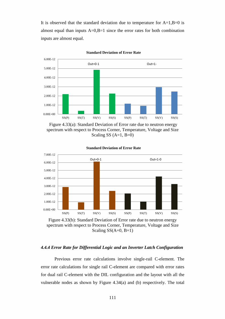
111
It is observed that the standard deviation due to temperature for A=1,B=0 is
almost equal than inputs A=0,B=1 since the error rates for both combination
inputs are almost equal.
Figure 4.33(a): Standard Deviation of Error rate due to neutron energy
spectrum with respect to Process Corner, Temperature, Voltage and Size
Scaling SS (A=1, B=0)
Figure 4.33(b): Standard Deviation of Error rate due to neutron energy
spectrum with respect to Process Corner, Temperature, Voltage and Size
Scaling SS(A=0, B=1)
4.4.4 Error Rate for Differential Logic and an Inverter Latch Configuration
Previous error rate calculations involve single-rail C-element. The
error rate calculations for single rail C-element are compared with error rates
for dual rail C-element with the DIL configuration and the layout with all the
vulnerable nodes as shown by Figure 4.34(a) and (b) respectively. The total
0.00E+00
1.00E-12
2.00E-12
3.00E-12
4.00E-12
5.00E-12
6.00E-12
SS(P) SS(T) SS(V) SS(S) SS(P) SS(T) SS(V) SS(S)
Standard Deviation of Error Rate
Out=0-1 Out=1-
0.00E+00
1.00E-12
2.00E-12
3.00E-12
4.00E-12
5.00E-12
6.00E-12
7.00E-12
SS(P) SS(T) SS(V) SS(S) SS(P) SS(T) SS(V) SS(S)
Standard Deviation of Error Rate
Out=0-1 Out=1-0
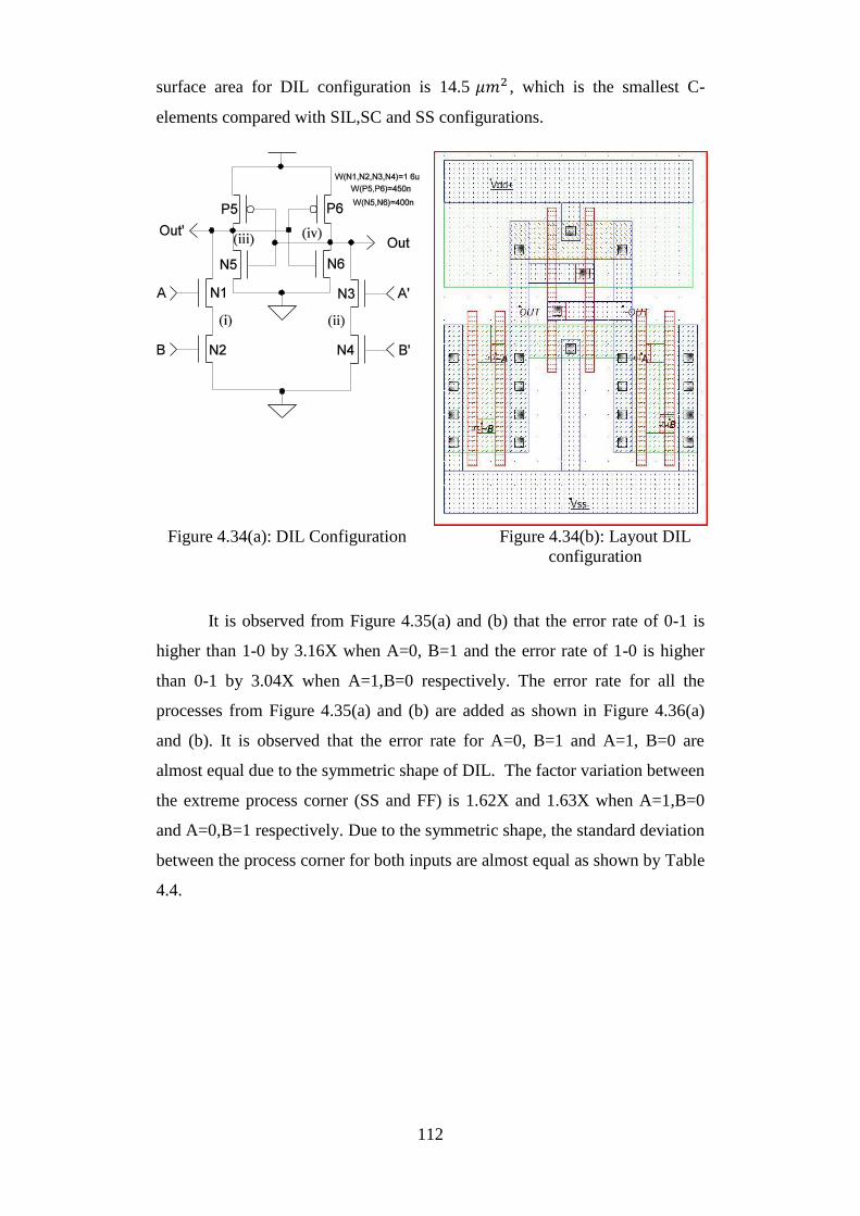
112
surface area for DIL configuration is 14.5 𝜇𝑚2 , which is the smallest C-
elements compared with SIL,SC and SS configurations.
Figure 4.34(a): DIL Configuration Figure 4.34(b): Layout DIL
configuration
It is observed from Figure 4.35(a) and (b) that the error rate of 0-1 is
higher than 1-0 by 3.16X when A=0, B=1 and the error rate of 1-0 is higher
than 0-1 by 3.04X when A=1,B=0 respectively. The error rate for all the
processes from Figure 4.35(a) and (b) are added as shown in Figure 4.36(a)
and (b). It is observed that the error rate for A=0, B=1 and A=1, B=0 are
almost equal due to the symmetric shape of DIL. The factor variation between
the extreme process corner (SS and FF) is 1.62X and 1.63X when A=1,B=0
and A=0,B=1 respectively. Due to the symmetric shape, the standard deviation
between the process corner for both inputs are almost equal as shown by Table
4.4.

113
No Process Corner Standard
Deveiation (σ)
Percentage
difference
w.r.t (i)
A=1 B=0 SS,FF 3.83E-12 -
TT,SNFP,FNSP 3.33E-13 8.7%
SS,FF,TT,SNFP,FNSP 2.44E-12 63.6%
A=0 B=1 SS,FF 3.8E-12 -
TT,SNFP,FNSP 3.33E-13 8.8%
SS,FF,TT,SNFP,FNSP 2.42E-12 63.6%
Table 4.4 : Standard Deviation for the Process Corner-DIL
Figure 4.35(a): Error rate due to neutron energy spectrum with respect to
Process Corner DIL(A=1, B=0)
Figure 4.35(b): Error rate due to neutron energy spectrum with respect to
Process Corner DIL(A=0, B=1)
0.00E+00
1.00E-12
2.00E-12
3.00E-12
4.00E-12
5.00E-12
6.00E-12
7.00E-12
8.00E-12
DIL (Error Rate /hr) vs Process Corner
Out=0-1 Out=1-0
0.00E+00
1.00E-12
2.00E-12
3.00E-12
4.00E-12
5.00E-12
6.00E-12
7.00E-12
8.00E-12
DIL (Error Rate /hr) vs Process Corner
Out=0-1 Out=1-0
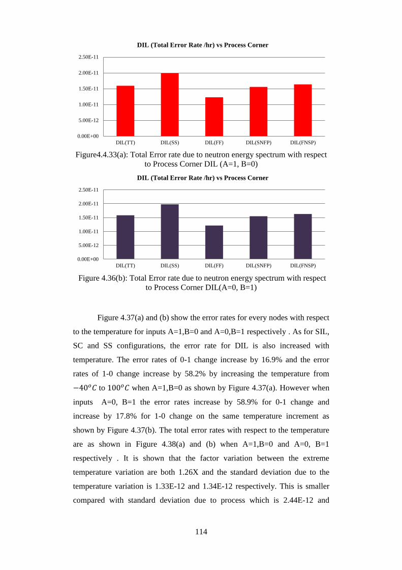
114
Figure4.4.33(a): Total Error rate due to neutron energy spectrum with respect
to Process Corner DIL (A=1, B=0)
Figure 4.36(b): Total Error rate due to neutron energy spectrum with respect
to Process Corner DIL(A=0, B=1)
Figure 4.37(a) and (b) show the error rates for every nodes with respect
to the temperature for inputs A=1,B=0 and A=0,B=1 respectively . As for SIL,
SC and SS configurations, the error rate for DIL is also increased with
temperature. The error rates of 0-1 change increase by 16.9% and the error
rates of 1-0 change increase by 58.2% by increasing the temperature from
−40𝑜𝐶 to 100𝑜𝐶 when A=1,B=0 as shown by Figure 4.37(a). However when
inputs A=0, B=1 the error rates increase by 58.9% for 0-1 change and
increase by 17.8% for 1-0 change on the same temperature increment as
shown by Figure 4.37(b). The total error rates with respect to the temperature
are as shown in Figure 4.38(a) and (b) when A=1,B=0 and A=0, B=1
respectively . It is shown that the factor variation between the extreme
temperature variation are both 1.26X and the standard deviation due to the
temperature variation is 1.33E-12 and 1.34E-12 respectively. This is smaller
compared with standard deviation due to process which is 2.44E-12 and
0.00E+00
5.00E-12
1.00E-11
1.50E-11
2.00E-11
2.50E-11
DIL(TT) DIL(SS) DIL(FF) DIL(SNFP) DIL(FNSP)
DIL (Total Error Rate /hr) vs Process Corner
0.00E+00
5.00E-12
1.00E-11
1.50E-11
2.00E-11
2.50E-11
DIL(TT) DIL(SS) DIL(FF) DIL(SNFP) DIL(FNSP)
DIL (Total Error Rate /hr) vs Process Corner
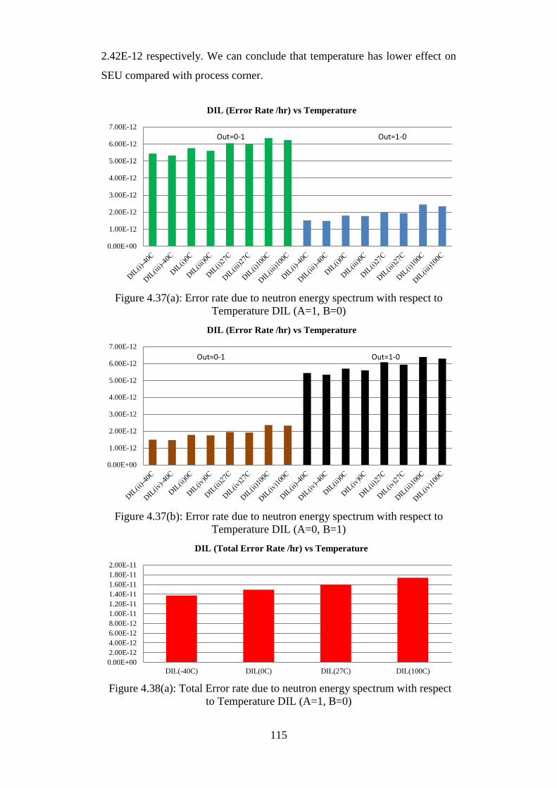
115
2.42E-12 respectively. We can conclude that temperature has lower effect on
SEU compared with process corner.
Figure 4.37(a): Error rate due to neutron energy spectrum with respect to
Temperature DIL (A=1, B=0)
Figure 4.37(b): Error rate due to neutron energy spectrum with respect to
Temperature DIL (A=0, B=1)
Figure 4.38(a): Total Error rate due to neutron energy spectrum with respect
to Temperature DIL (A=1, B=0)
0.00E+00
1.00E-12
2.00E-12
3.00E-12
4.00E-12
5.00E-12
6.00E-12
7.00E-12
DIL (Error Rate /hr) vs Temperature
Out=0-1 Out=1-0
0.00E+00
1.00E-12
2.00E-12
3.00E-12
4.00E-12
5.00E-12
6.00E-12
7.00E-12
DIL (Error Rate /hr) vs Temperature
Out=0-1 Out=1-0
0.00E+00
2.00E-12
4.00E-12
6.00E-12
8.00E-12
1.00E-11
1.20E-11
1.40E-11
1.60E-11
1.80E-11
2.00E-11
DIL(-40C) DIL(0C) DIL(27C) DIL(100C)
DIL (Total Error Rate /hr) vs Temperature
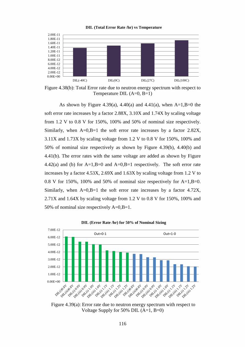
116
Figure 4.38(b): Total Error rate due to neutron energy spectrum with respect to
Temperature DIL (A=0, B=1)
As shown by Figure 4.39(a), 4.40(a) and 4.41(a), when A=1,B=0 the
soft error rate increases by a factor 2.88X, 3.10X and 1.74X by scaling voltage
from 1.2 V to 0.8 V for 150%, 100% and 50% of nominal size respectively.
Similarly, when A=0,B=1 the soft error rate increases by a factor 2.82X,
3.11X and 1.73X by scaling voltage from 1.2 V to 0.8 V for 150%, 100% and
50% of nominal size respectively as shown by Figure 4.39(b), 4.40(b) and
4.41(b). The error rates with the same voltage are added as shown by Figure
4.42(a) and (b) for A=1,B=0 and A=0,B=1 respectively. The soft error rate
increases by a factor 4.53X, 2.69X and 1.63X by scaling voltage from 1.2 V to
0.8 V for 150%, 100% and 50% of nominal size respectively for A=1,B=0.
Similarly, when A=0,B=1 the soft error rate increases by a factor 4.72X,
2.71X and 1.64X by scaling voltage from 1.2 V to 0.8 V for 150%, 100% and
50% of nominal size respectively A=0,B=1.
Figure 4.39(a): Error rate due to neutron energy spectrum with respect to
Voltage Supply for 50% DIL (A=1, B=0)
0.00E+00
2.00E-12
4.00E-12
6.00E-12
8.00E-12
1.00E-11
1.20E-11
1.40E-11
1.60E-11
1.80E-11
2.00E-11
DIL(-40C) DIL(0C) DIL(27C) DIL(100C)
DIL (Total Error Rate /hr) vs Temperature
0.00E+00
1.00E-12
2.00E-12
3.00E-12
4.00E-12
5.00E-12
6.00E-12
7.00E-12
DIL (Error Rate /hr) for 50% of Nominal Sizing
Out=0-1 Out=1-0

117
Figure 4.39(b): Error rate due to neutron energy spectrum with respect to
Voltage Supply for 50% DIL (A=0, B=1)
Figure 4.40(a): Error rate due to neutron energy spectrum with respect to
Voltage Supply for 100% DIL (A=1, B=0)
Figure 4.40(b): Error rate due to neutron energy spectrum with respect to
Voltage Supply for 100% DIL (A=0, B=1)
0.00E+00
1.00E-12
2.00E-12
3.00E-12
4.00E-12
5.00E-12
6.00E-12
7.00E-12
DIL (Error Rate /hr) for 50% of Nominal Sizing
Out=0-1 Out=1-0
0.00E+00
1.00E-12
2.00E-12
3.00E-12
4.00E-12
5.00E-12
6.00E-12
7.00E-12
8.00E-12
9.00E-12
1.00E-11
DIL (Error Rate /hr) for 100% of Nominal Sizing
Out=0-1 Out=1-0
0.00E+00
1.00E-12
2.00E-12
3.00E-12
4.00E-12
5.00E-12
6.00E-12
7.00E-12
8.00E-12
9.00E-12
1.00E-11
DIL (Error Rate /hr) for 100% of Nominal Sizing
Out=0-1 Out=1-0

118
Figure 4.41(a): Error rate due to neutron energy spectrum with respect to
Voltage Supply for 150% DIL (A=1, B=0)
Figure 4.41(b): Error rate due to neutron energy spectrum with respect to
Voltage Supply for 150% DIL (A=0, B=1)
Figure 4.42(a): Total error rate due to neutron energy spectrum with respect to
Voltage Supply for DIL (A=1, B=0)
0.00E+00
5.00E-13
1.00E-12
1.50E-12
2.00E-12
2.50E-12
3.00E-12
3.50E-12
4.00E-12
4.50E-12
5.00E-12
DIL (Error Rate /hr) for 150% of Nominal Sizing
Out=0-1 Out=1-0
0.00E+00
5.00E-13
1.00E-12
1.50E-12
2.00E-12
2.50E-12
3.00E-12
3.50E-12
4.00E-12
4.50E-12
5.00E-12
DIL (Error Rate /hr) for 150% of Nominal Sizing
Out=0-1 Out=1-
0.00E+00
5.00E-12
1.00E-11
1.50E-11
2.00E-11
2.50E-11
3.00E-11
Total Error Rate (/hr) of Different Sizing DIL
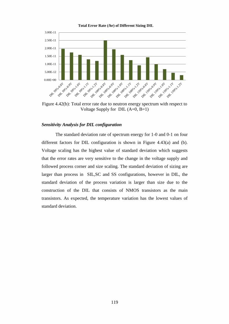
119
Figure 4.42(b): Total error rate due to neutron energy spectrum with respect to
Voltage Supply for DIL (A=0, B=1)
Sensitivity Analysis for DIL configuration
The standard deviation rate of spectrum energy for 1-0 and 0-1 on four
different factors for DIL configuration is shown in Figure 4.43(a) and (b).
Voltage scaling has the highest value of standard deviation which suggests
that the error rates are very sensitive to the change in the voltage supply and
followed process corner and size scaling. The standard deviation of sizing are
larger than process in SIL,SC and SS configurations, however in DIL, the
standard deviation of the process variation is larger than size due to the
construction of the DIL that consists of NMOS transistors as the main
transistors. As expected, the temperature variation has the lowest values of
standard deviation.
0.00E+00
5.00E-12
1.00E-11
1.50E-11
2.00E-11
2.50E-11
3.00E-11
Total Error Rate (/hr) of Different Sizing DIL

120
Figure 4.43(a): Standard Deviation of Error rate due to neutron energy
spectrum with respect to Process Corner, Temperature, Voltage Scaling and
Sizing DIL(A=1, B=0)
Figure 4.43(b): Standard Deviation of Error rate due to neutron energy
spectrum with respect to Process Corner, Temperature, Voltage Scaling and
Sizing DIL(A=0, B=1)
4.5 Circuit Vulnerability Against Single Event Upset -Error Rate
In Chapter 3 two methods are used in order to compare the vulnerability of C-
elements with respect to SEU which are comparing the normalised critical
charge at the output of C-elements (Out) and the node sensitivity by
calculating the standard deviation of the critical charges. In this chapter, the
vulnerability of C-elements with respect to SEU are obtained by comparing
0.00E+00
5.00E-13
1.00E-12
1.50E-12
2.00E-12
2.50E-12
3.00E-12
3.50E-12
4.00E-12
DIL(P) DIL(T) DIL(V) DIL(S) DIL(P) DIL(T) DIL(V) DIL(S)
Standard Deviation of Error Rate
Out=0-1
0.00E+00
5.00E-13
1.00E-12
1.50E-12
2.00E-12
2.50E-12
3.00E-12
3.50E-12
4.00E-12
DIL(P) DIL(T) DIL(V) DIL(S) DIL(P) DIL(T) DIL(V) DIL(S)
Standard Deviation of Error Rate
Out=0-1

121
the total error rate and standard deviation of the error rate with different
parameters as described before.
4.5.1 Error Rate Comparisons
The total error rate for A=1,B=0 and A=0, B=1 are added for all
configuration of C-Elements . The sums of total error are compared with
respect to process, temperature and voltage variations as shown by Figure
4.44-4.46. From Figure 4.44, factor variations of error rate between SS and
FF are 1.67, 1.47, 1.82 and 1.62 for SIL,SC,SS and DIL respectively. SS has
the highest factor variation between extreme process and SC has the lowest
factor variation. This shows that SS is sensitive with process variation
compared with other configurations. From Figure 4.45, factor variations of
error rates from -40 C to 100 C are 1.26, 1.17, 1.24 and 1.26 for SIL,SC,SS
and DIL respectively. SC and DIL has the highest factor variation between
extreme temperature and SC has the lowest factor variation. This shows that
SIL and DIL are sensitive with process variation compared with other
configurations. From Figure 4.46, factor variations of error rate from 0.8 V to
1.2 V are 3.25, 2.26, 3.31 and 2.71 for SIL,SC,SS and DIL respectively. SS
has the highest factor variation between extreme voltage and SC has the
lowest factor variation. This shows that SS is sensitive with voltage variation
compared with other configurations
Figure 4.44: Comparison of total error rate due to neutron energy spectrum
with respect to process at nominal sizing
0
1E-11
2E-11
3E-11
4E-11
5E-11
6E-11
Total Error Rate with respect to Process

122
Figure 4.45: Comparison of total error rate due to neutron energy spectrum
with respect to temperature at nominal sizing
Figure 4.46: Comparison of total error rate due to neutron energy spectrum
with respect to voltage at nominal sizing
It is obvious that SS has the highest error rate compared with other
configurations. SC and SS have the same number of transistors. However due
to the constructions of SS has more vulnerable nodes to soft error compared
with SC. SIL has the lowest error rates compared with others and therefore
more resistant towards soft error.
4.5.2 Sensitivity Analysis
The comparison of nodes sensitivity with respect to the process corner
variation, temperature, voltage and size scaling are presented as shown in
0
5E-12
1E-11
1.5E-11
2E-11
2.5E-11
3E-11
3.5E-11
4E-11
4.5E-11
5E-11
Total Error Rate with respect to Temperature
0
1E-11
2E-11
3E-11
4E-11
5E-11
6E-11
7E-11
8E-11
Total Error Rate with respect to Voltage at Nominal size
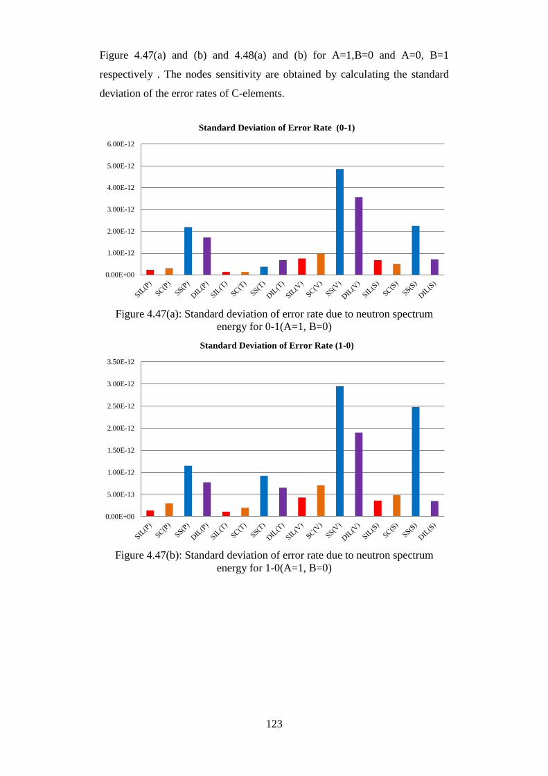
123
Figure 4.47(a) and (b) and 4.48(a) and (b) for A=1,B=0 and A=0, B=1
respectively . The nodes sensitivity are obtained by calculating the standard
deviation of the error rates of C-elements.
Figure 4.47(a): Standard deviation of error rate due to neutron spectrum
energy for 0-1(A=1, B=0)
Figure 4.47(b): Standard deviation of error rate due to neutron spectrum
energy for 1-0(A=1, B=0)
0.00E+00
1.00E-12
2.00E-12
3.00E-12
4.00E-12
5.00E-12
6.00E-12
Standard Deviation of Error Rate (0-1)
0.00E+00
5.00E-13
1.00E-12
1.50E-12
2.00E-12
2.50E-12
3.00E-12
3.50E-12
Standard Deviation of Error Rate (1-0)
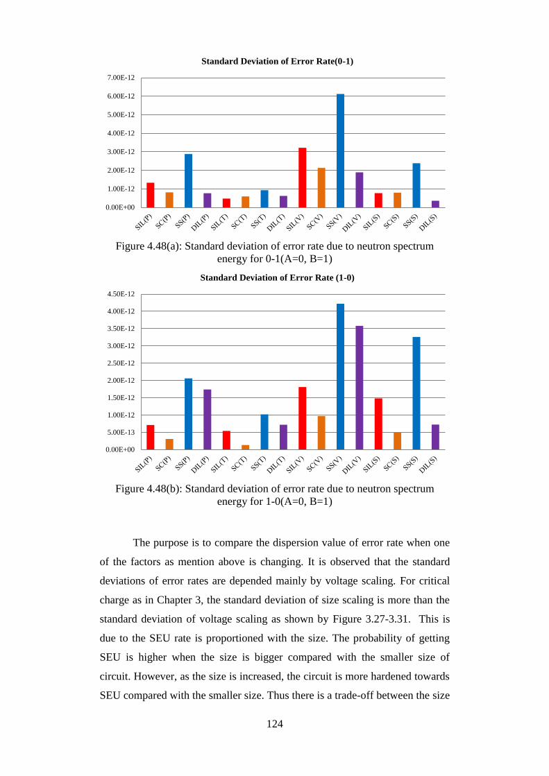
124
Figure 4.48(a): Standard deviation of error rate due to neutron spectrum
energy for 0-1(A=0, B=1)
Figure 4.48(b): Standard deviation of error rate due to neutron spectrum
energy for 1-0(A=0, B=1)
The purpose is to compare the dispersion value of error rate when one
of the factors as mention above is changing. It is observed that the standard
deviations of error rates are depended mainly by voltage scaling. For critical
charge as in Chapter 3, the standard deviation of size scaling is more than the
standard deviation of voltage scaling as shown by Figure 3.27-3.31. This is
due to the SEU rate is proportioned with the size. The probability of getting
SEU is higher when the size is bigger compared with the smaller size of
circuit. However, as the size is increased, the circuit is more hardened towards
SEU compared with the smaller size. Thus there is a trade-off between the size
0.00E+00
1.00E-12
2.00E-12
3.00E-12
4.00E-12
5.00E-12
6.00E-12
7.00E-12
Standard Deviation of Error Rate(0-1)
0.00E+00
5.00E-13
1.00E-12
1.50E-12
2.00E-12
2.50E-12
3.00E-12
3.50E-12
4.00E-12
4.50E-12
Standard Deviation of Error Rate (1-0)

125
of the circuit and the error rate. The temperature is the least factors that can
vary the error rate. In general, SS configuration has the highest standard
deviation compared with other configuration and therefore the least stable
against four factors (Process corner, temperature, voltage and size scaling).
This is due to the construction of circuit which has the most number of
vulnerable nodes and hence the highest error rate. Any variation of the highest
error rate will contribute to the highest standard deviations. We can conclude
that SIL and SC configurations are the most stable configurations against SEU
since the standard deviation values are lower compared with SS and DIL
configurations. In contrast, the SIL configuration is the least stable as shown
by Figure 3.27-3.31 in Chapter 3, only if the value of critical charge is taking
into account. However, after the overall size of is taking into consideration the
standard deviation of error rate of SIL is lower compared with SS and DIL.
4.6 Conclusions
In this chapter, we developed a method to calculate the error rate due
to neutron energy spectrum at different nodes and with different
implementation of C-elements. As in Chapter 3, there are four different factors
that we used to study the error rate: Process corner, temperature, voltage and
size scaling. Voltage scaling has the highest value of standard deviation which
suggests that the error rates are very sensitive to the change in the voltage
supply and followed process corner and size scaling. Our calculation and
observation shows that the most significant factors of error rate is voltage
scaling. This is in contrast with the standard deviation for critical charge found
in Chapter 3 that suggest size has the highest standard deviation compared
with voltage scaling. This is due to the SEU rate is proportioned with the size.
As the size is increased, the circuit is more resistant against SEU compared
with the smaller size, however, the probability of hitting by SEU is also
increased.The standard deviation of sizing are larger than process in SIL,SC
and SS configurations, however in DIL, the standard deviation of the process
variation is larger than size due to the construction of the DIL that consists of
NMOS transistors as the main transistors. As expected, the temperature
variation has the lowest values of standard deviation. In general, it is observed
that the SS and DIL have the most error rate compared with SIL and SC. SIL

126
has the lowest error rate. Therefore in general, the standard deviations for SS
and DIL are higher compared with SC and SIL.

127
Chapter 5. Error Detection and Correction of Single Event
Upset Tolerant Latch for Single Rail Data
This chapter presents an error detection latch (ED) design and error detection
and correction latch (EDC). The functionality of both ED and EDC latches are
demonstrated using Cadence UMC 90nm. The waveforms under fault free
conditions and in the event of an SEU striking the vulnerable nodes are
obtained. The performance of ED and EDC latches are analysed in terms of
propagation delay and switching power.
5.1 Introduction
The mitigation of soft error in digital circuit is one of the important
research area in modern integrated circuit. It is desireable to construct a latch
which is not only can detect errors, but also has the capability of correcting
them. In this chapter, the fault-tolerant latch based on C-element is proposed
since it can hold the signal data and control data independently. The latch is
designed based on Razor flip-flop.
The concepts of a Razor flip flop [58] is harnassed in the proposed
latch to restore the correct values in the event of a particle strike that might
possibly corrupt data. The operation of Razor flip-flop can be summarized as
follows. Razor flip flop consists of main latch, shadow latch, comparator and
MUX as shown in Figure 5.1. In the event of the delay in the combinational
logic meets the setup time of the rising edge of clock, the correct data is
latched by the main flip-flop and shadow latch. The output of main flip-flop
and shadow latch is compared and since the timing requirement is met, no
error is detected. However, in the event of the delay in the combinational logic
becomes significant, the data is not latched by the main flip flop. Due to the
delayed clock, the data is latched by shadow latch. The output of main flip
flop is compared with the shadow latch and since it is not equal, the
multiplexer (MUX) switch the value to allow the output of shadow latch to
propagate to the main latch. The valid data is restored in the next cycle of
clock. One of the problems of Razor flip-flop is the existence of short path
between the clock and the delayed clock. This can lead to the corruption of the
data in the shadow latch, and the minimum-path length constraint is added at
the input of each Razor flip-flop in the design.
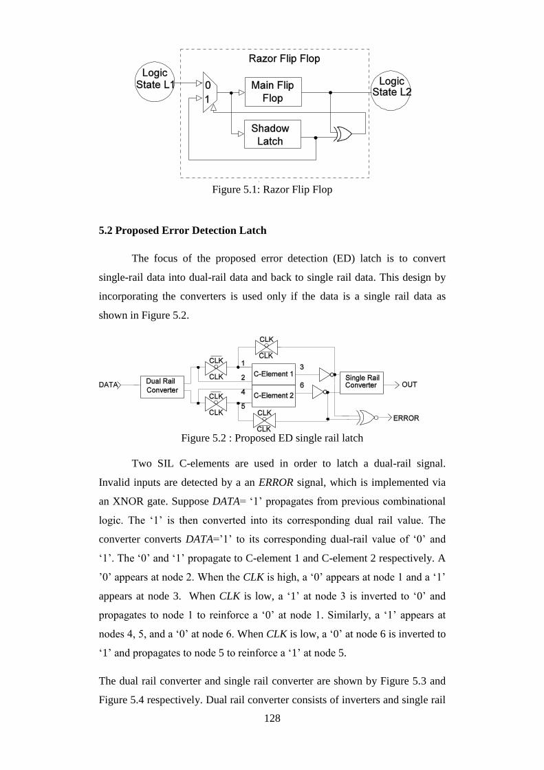
128
Figure 5.1: Razor Flip Flop
5.2 Proposed Error Detection Latch
The focus of the proposed error detection (ED) latch is to convert
single-rail data into dual-rail data and back to single rail data. This design by
incorporating the converters is used only if the data is a single rail data as
shown in Figure 5.2.
Figure 5.2 : Proposed ED single rail latch
Two SIL C-elements are used in order to latch a dual-rail signal.
Invalid inputs are detected by a an ERROR signal, which is implemented via
an XNOR gate. Suppose DATA= ‘1’ propagates from previous combinational
logic. The ‘1’ is then converted into its corresponding dual rail value. The
converter converts DATA=’1’ to its corresponding dual-rail value of ‘0’ and
‘1’. The ‘0’ and ‘1’ propagate to C-element 1 and C-element 2 respectively. A
’0’ appears at node 2. When the CLK is high, a ‘0’ appears at node 1 and a ‘1’
appears at node 3. When CLK is low, a ‘1’ at node 3 is inverted to ‘0’ and
propagates to node 1 to reinforce a ‘0’ at node 1. Similarly, a ‘1’ appears at
nodes 4, 5, and a ‘0’ at node 6. When CLK is low, a ‘0’ at node 6 is inverted to
‘1’ and propagates to node 5 to reinforce a ‘1’ at node 5.
The dual rail converter and single rail converter are shown by Figure 5.3 and
Figure 5.4 respectively. Dual rail converter consists of inverters and single rail
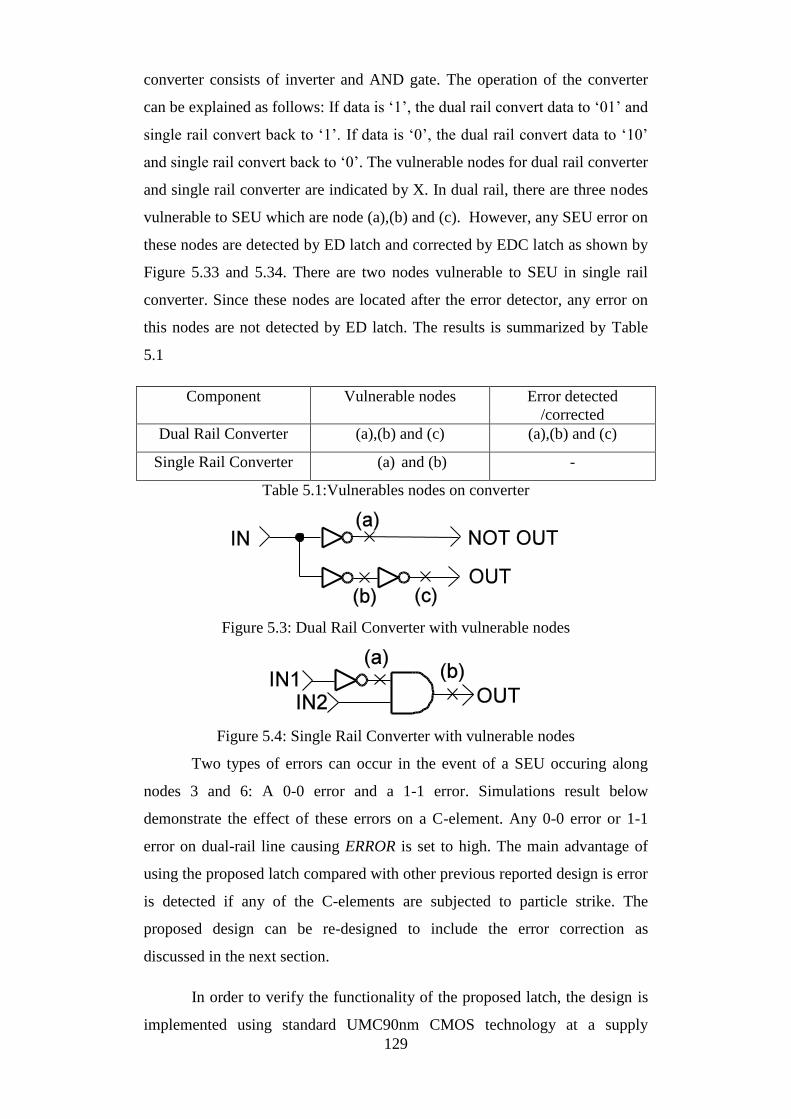
129
converter consists of inverter and AND gate. The operation of the converter
can be explained as follows: If data is ‘1’, the dual rail convert data to ‘01’ and
single rail convert back to ‘1’. If data is ‘0’, the dual rail convert data to ‘10’
and single rail convert back to ‘0’. The vulnerable nodes for dual rail converter
and single rail converter are indicated by X. In dual rail, there are three nodes
vulnerable to SEU which are node (a),(b) and (c). However, any SEU error on
these nodes are detected by ED latch and corrected by EDC latch as shown by
Figure 5.33 and 5.34. There are two nodes vulnerable to SEU in single rail
converter. Since these nodes are located after the error detector, any error on
this nodes are not detected by ED latch. The results is summarized by Table
5.1
Component Vulnerable nodes Error detected
/corrected
Dual Rail Converter (a),(b) and (c) (a),(b) and (c)
Single Rail Converter (a) and (b) -
Table 5.1:Vulnerables nodes on converter
Figure 5.3: Dual Rail Converter with vulnerable nodes
Figure 5.4: Single Rail Converter with vulnerable nodes
Two types of errors can occur in the event of a SEU occuring along
nodes 3 and 6: A 0-0 error and a 1-1 error. Simulations result below
demonstrate the effect of these errors on a C-element. Any 0-0 error or 1-1
error on dual-rail line causing ERROR is set to high. The main advantage of
using the proposed latch compared with other previous reported design is error
is detected if any of the C-elements are subjected to particle strike. The
proposed design can be re-designed to include the error correction as
discussed in the next section.
In order to verify the functionality of the proposed latch, the design is
implemented using standard UMC90nm CMOS technology at a supply
130
voltage, 𝑉𝐷𝐷 of 1 V. The Faraday circuit library is used in the design and the
design of C-element performed via the use of PMOS and NMOS transistors,
with the sizing ratio set to (1.8𝑢𝑚
90𝑛𝑚) and (
1.6𝑢𝑚
90𝑛𝑚) respectively. The aspect ratio of
PMOS with NMOS is 1.12 and according to standard inverter ratio in Faraday
library. The behaviours of the circuits are verified by simulation with nominal
values for electrical parameters.
The simulation for the case of fault-free and error detected operation at
the middle of the functional signal is shown in Figure 5.5. Time T1 shows the
waveform for the fault-free condition. A single rail data signal is converted
into a dual rail data signal before it is converted to single rail. No error is
detected. The data propagates succesful to the output of the latch. At time T2
as shown in (a) illustrate node 6 is injecting with current pulse at the middle of
the functional signal causing the output of C-element 2 changing from 0 to 1
temporarily. Node 3 remains undisturbed. As a result, this causes a 1-1 error
and this data is considered invalid and is marked as erroneous as shown in (c).
The output, OUT, changes temporarily from 1 to 0 as shown in (e).Similarly,
node 3 is injecting with current pulse at the middle of the functional signal
causing the output of C-element 1 changes temporarily from 1 to 0 as shown
in (b) at time T3. Node 6 remains undisturbed. As a result, this causes a 0-0
error and this data is considered invalid and marked as erroneous as shown in
(d). The output, OUT, changes temporarily from 1 to 0 as shown in (f). For 1-
1 error and 0-0 error, the ERROR is high to indicate that SEU error taking
place at node 3 and node 6 of C-elements.
The simulation is repeated for the case of error detected operation at
the edge of the functional signal as shown in Figure 5.6. At time T2 illustrate
node 3 is injecting with current pulse at the edge of the functional signal
causing the output of C-element 1 changing from 1 to 0 temporarily and thus
creating 0-0 error as shown in (a). The output, OUT, changes temporarily from
1 to 0 as shown in (e).Similarly node 6 is injecting with current pulse at the
edge of the functional signal causing the output of C-element 2 changes
temporarily from 0 to 1 at time T3 and thus creating 1-1 error as shown in (b).
The output, OUT, changes temporarily from 1 to 0 as shown in (f). For 1-1
error and 0-0 error, the ERROR is high to indicate that SEU error taking place
at node 3 and node 6 of C-elements as shown by (c) and (d) respectively
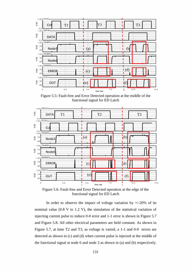
131
Figure 5.5: Fault-free and Error Detected operation at the middle of the
functional signal for ED Latch
Figure 5.6: Fault-free and Error Detected operation at the edge of the
functional signal for ED Latch
In order to observe the impact of voltage variation by +/-20% of its
nominal value (0.8 V to 1.2 V), the simulation of the statistical variation of
injecting current pulse to induce 0-0 error and 1-1 error is shown in Figure 5.7
and Figure 5.8. All other electrical parameters are held constant. As shown in
Figure 5.7, at time T2 and T3, as voltage is varied, a 1-1 and 0-0 errors are
detected as shown in (c) and (d) when current pulse is injected at the middle of
the functional signal at node 6 and node 3 as shown in (a) and (b) respectively.
CLK
DATA
Node3
Node6
ERROR
OUT
T1 T2 T3
(a) (b
)
(c) (d)
(e) (f)
DATA
CLK
Node3
Node6
ERROR
OUT
T1 T2 T3
(a) (b)
(c) (d)
(e) (f)
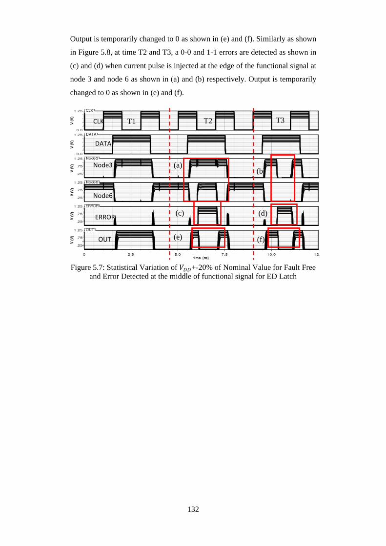
132
Output is temporarily changed to 0 as shown in (e) and (f). Similarly as shown
in Figure 5.8, at time T2 and T3, a 0-0 and 1-1 errors are detected as shown in
(c) and (d) when current pulse is injected at the edge of the functional signal at
node 3 and node 6 as shown in (a) and (b) respectively. Output is temporarily
changed to 0 as shown in (e) and (f).
Figure 5.7: Statistical Variation of 𝑉𝐷𝐷+-20% of Nominal Value for Fault Free
and Error Detected at the middle of functional signal for ED Latch
CLK
DATA
Node3
Node6
ERROR
OUT
T1 T2 T3
(a) (b)
(c) (d)
(e) (f)
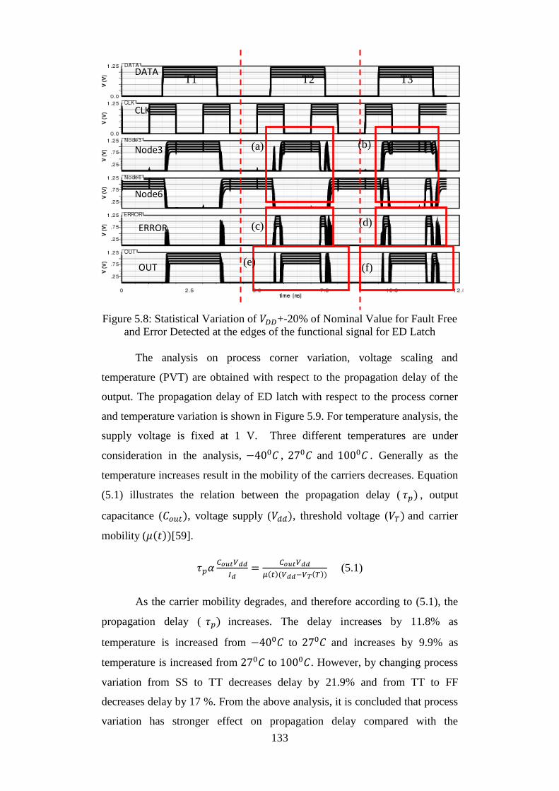
133
Figure 5.8: Statistical Variation of 𝑉𝐷𝐷+-20% of Nominal Value for Fault Free
and Error Detected at the edges of the functional signal for ED Latch
The analysis on process corner variation, voltage scaling and
temperature (PVT) are obtained with respect to the propagation delay of the
output. The propagation delay of ED latch with respect to the process corner
and temperature variation is shown in Figure 5.9. For temperature analysis, the
supply voltage is fixed at 1 V. Three different temperatures are under
consideration in the analysis, −400𝐶 , 270𝐶 and 1000𝐶 . Generally as the
temperature increases result in the mobility of the carriers decreases. Equation
(5.1) illustrates the relation between the propagation delay ( 𝜏𝑝) , output
capacitance (𝐶𝑜𝑢𝑡), voltage supply (𝑉𝑑𝑑), threshold voltage (𝑉𝑇) and carrier
mobility (𝜇(𝑡))[59].
𝜏𝑝𝛼𝐶𝑜𝑢𝑡𝑉𝑑𝑑
𝐼𝑑=
𝐶𝑜𝑢𝑡𝑉𝑑𝑑
𝜇(𝑡)(𝑉𝑑𝑑−𝑉𝑇(𝑇)) (5.1)
As the carrier mobility degrades, and therefore according to (5.1), the
propagation delay ( 𝜏𝑝) increases. The delay increases by 11.8% as
temperature is increased from −400𝐶 to 270𝐶 and increases by 9.9% as
temperature is increased from 270𝐶 to 1000𝐶. However, by changing process
variation from SS to TT decreases delay by 21.9% and from TT to FF
decreases delay by 17 %. From the above analysis, it is concluded that process
variation has stronger effect on propagation delay compared with the
DATA
CLK
Node3
Node6
ERROR
OUT
T1 T2 T3
(a) (b)
(c) (d)
(e) (f)
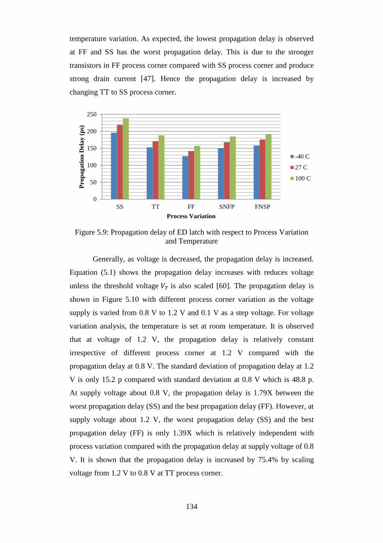
134
temperature variation. As expected, the lowest propagation delay is observed
at FF and SS has the worst propagation delay. This is due to the stronger
transistors in FF process corner compared with SS process corner and produce
strong drain current [47]. Hence the propagation delay is increased by
changing TT to SS process corner.
Figure 5.9: Propagation delay of ED latch with respect to Process Variation
and Temperature
Generally, as voltage is decreased, the propagation delay is increased.
Equation (5.1) shows the propagation delay increases with reduces voltage
unless the threshold voltage 𝑉𝑇 is also scaled [60]. The propagation delay is
shown in Figure 5.10 with different process corner variation as the voltage
supply is varied from 0.8 V to 1.2 V and 0.1 V as a step voltage. For voltage
variation analysis, the temperature is set at room temperature. It is observed
that at voltage of 1.2 V, the propagation delay is relatively constant
irrespective of different process corner at 1.2 V compared with the
propagation delay at 0.8 V. The standard deviation of propagation delay at 1.2
V is only 15.2 p compared with standard deviation at 0.8 V which is 48.8 p.
At supply voltage about 0.8 V, the propagation delay is 1.79X between the
worst propagation delay (SS) and the best propagation delay (FF). However, at
supply voltage about 1.2 V, the worst propagation delay (SS) and the best
propagation delay (FF) is only 1.39X which is relatively independent with
process variation compared with the propagation delay at supply voltage of 0.8
V. It is shown that the propagation delay is increased by 75.4% by scaling
voltage from 1.2 V to 0.8 V at TT process corner.
0
50
100
150
200
250
SS TT FF SNFP FNSP
Pro
pa
ga
tio
n D
ela
y (
ps)
Process Variation
-40 C
27 C
100 C
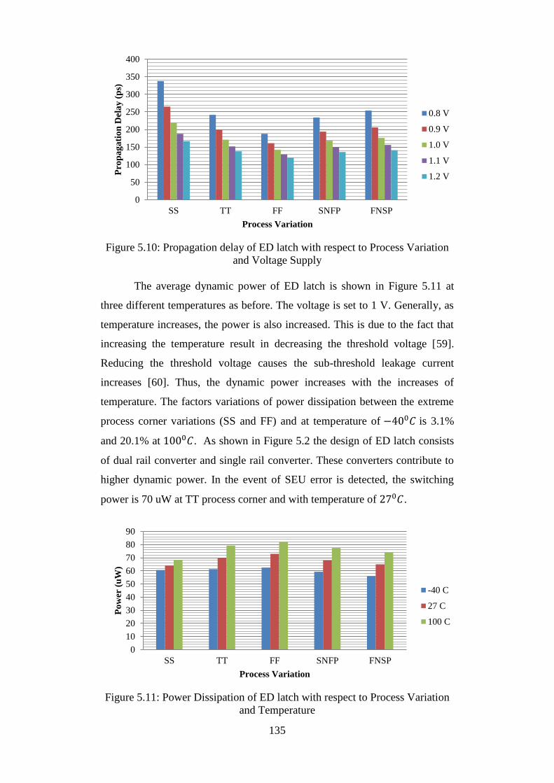
135
Figure 5.10: Propagation delay of ED latch with respect to Process Variation
and Voltage Supply
The average dynamic power of ED latch is shown in Figure 5.11 at
three different temperatures as before. The voltage is set to 1 V. Generally, as
temperature increases, the power is also increased. This is due to the fact that
increasing the temperature result in decreasing the threshold voltage [59].
Reducing the threshold voltage causes the sub-threshold leakage current
increases [60]. Thus, the dynamic power increases with the increases of
temperature. The factors variations of power dissipation between the extreme
process corner variations (SS and FF) and at temperature of −400𝐶 is 3.1%
and 20.1% at 1000𝐶. As shown in Figure 5.2 the design of ED latch consists
of dual rail converter and single rail converter. These converters contribute to
higher dynamic power. In the event of SEU error is detected, the switching
power is 70 uW at TT process corner and with temperature of 270𝐶.
Figure 5.11: Power Dissipation of ED latch with respect to Process Variation
and Temperature
0
50
100
150
200
250
300
350
400
SS TT FF SNFP FNSP
Pro
pa
ga
tio
n D
ela
y (
ps)
Process Variation
0.8 V
0.9 V
1.0 V
1.1 V
1.2 V
0
10
20
30
40
50
60
70
80
90
SS TT FF SNFP FNSP
Po
wer
(u
W)
Process Variation
-40 C
27 C
100 C

136
We can characterize the switching energy of the circuit with respect of current
pulse causing SEU charge into 3 distinct regions
a) Pre-critical charges that cause small change to the switching energy –
Over a small range of input pulse amplitude, the pulse output is
generated. The energy of the circuit increases slightly with the
increases of the current charge.
b) Critical charge that causes significant change to the switching energy –
At certain amplitude of current pulse, the state holder may change its
state. The energy is suddenly increased its value significantly. At this
point, the amount of charge that change the state holder is known as
the critical charge and it varies from node to node.
c) Post-critical charge that cause small change to the switching energy –
When the current charge is higher than critical charge, it cause the
switching energy to increase slightly.
The SEU charge is varied by varying the amplitude of induced SEU
until the state at node 3 and node 6 are changed. The switching energy of the
circuit for 0-1 change by inducing node 6 with SEU and 1-0 change by
inducing node 3 with SEU with respect to the process corner are shown in
Figure 5.12 and Figure 5.13. In this simulation, switching energy of the circuit
is measured with different process variations-SS, TT and FF. The SS, TT and
FF process variation are chosen as to compare the worst (SS), typical (TT) and
the best (FF) values of switching energy with respect to the critical charge
injected into the node. The temperature is set to 270𝐶 and the supply voltage
is 1 V. From Figure 5.12 for 0-1 change, it is shown that the SS has the lowest
critical charge value of 26 fC, TT has the critical charge of 35 fC and FF has
the highest critical charge value of 38 fC. From Figure 5.13 for 1-0 change,
the corresponding values of critical charges are 52 fC, 61 fC and 70 fC for SS,
TT and FF respectively. The critical charges for 1-0 change are double
compared with 0-1 change due to NMOS transistor is 2.2 times more sensitive
compared with PMOS transistor for the same width [54]. For 0-1 change, the
SS has lowest maximum switching energy (100 fJ) compared with TT (109 fJ)
and FF (123 FJ). For 1-0 change, the corresponding maximum switching
energy values are 66 fJ, 70 fJ and 78 fJ for SS, TT and FF respectively. The

137
factor variation of switching energy between extreme process variation (FF
and SS) is 1.23X for 0-1 change and 1.32X for 1-0 change. The higher
maximum switching energy by 0-1 change is due to the lower gate leakage
current in PMOS compared with NMOS [61] and therefore contributes to the
higher switching energy for 0-1 change. It is observed that the latch has the
initial switching energy values of 21.4 fJ (SS), 24.5 fJ (TT) and 25 fJ (FF)
corresponding to the no current pulse injected into the node. The higher initial
energy values are due to the switching activity of the single rail and dual rail
converters.
Figure 5.12: Switching Energy for ED Latch (0-1 Change) with Different
Process
Figure 5.13: Switching Energy for ED Latch (1-0 Change) with Different
Process
0
20
40
60
80
100
120
0 10 20 30 40
Sw
itch
ing
En
erg
y (
fJ)
SEU Charge (fC)
SS
TT
FF
0
10
20
30
40
50
60
70
80
90
100
46.8 51.8 56.8 61.8 66.8 71.8 76.8
Sw
itch
ing
En
erg
y (
fJ)
SEU Charge (fC)
SS
TT
FF
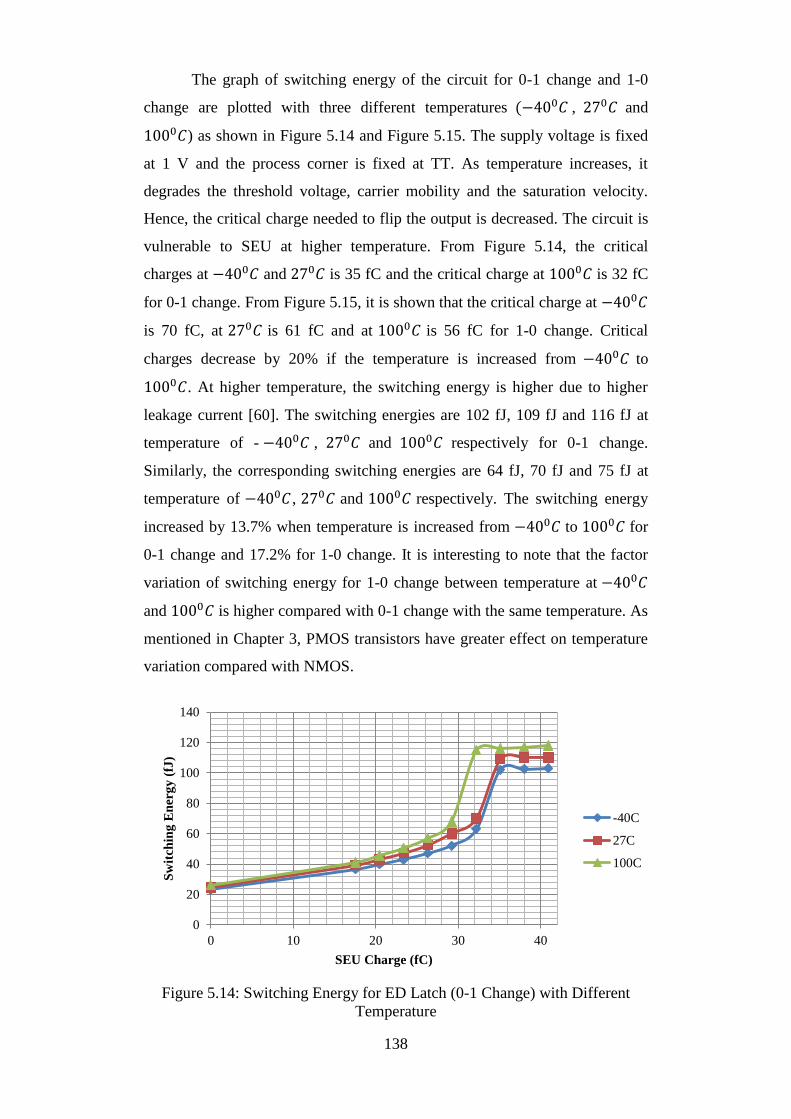
138
The graph of switching energy of the circuit for 0-1 change and 1-0
change are plotted with three different temperatures (−400𝐶 , 270𝐶 and
1000𝐶) as shown in Figure 5.14 and Figure 5.15. The supply voltage is fixed
at 1 V and the process corner is fixed at TT. As temperature increases, it
degrades the threshold voltage, carrier mobility and the saturation velocity.
Hence, the critical charge needed to flip the output is decreased. The circuit is
vulnerable to SEU at higher temperature. From Figure 5.14, the critical
charges at −400𝐶 and 270𝐶 is 35 fC and the critical charge at 1000𝐶 is 32 fC
for 0-1 change. From Figure 5.15, it is shown that the critical charge at −400𝐶
is 70 fC, at 270𝐶 is 61 fC and at 1000𝐶 is 56 fC for 1-0 change. Critical
charges decrease by 20% if the temperature is increased from −400𝐶 to
1000𝐶. At higher temperature, the switching energy is higher due to higher
leakage current [60]. The switching energies are 102 fJ, 109 fJ and 116 fJ at
temperature of - −400𝐶 , 270𝐶 and 1000𝐶 respectively for 0-1 change.
Similarly, the corresponding switching energies are 64 fJ, 70 fJ and 75 fJ at
temperature of −400𝐶 , 270𝐶 and 1000𝐶 respectively. The switching energy
increased by 13.7% when temperature is increased from −400𝐶 to 1000𝐶 for
0-1 change and 17.2% for 1-0 change. It is interesting to note that the factor
variation of switching energy for 1-0 change between temperature at −400𝐶
and 1000𝐶 is higher compared with 0-1 change with the same temperature. As
mentioned in Chapter 3, PMOS transistors have greater effect on temperature
variation compared with NMOS.
Figure 5.14: Switching Energy for ED Latch (0-1 Change) with Different
Temperature
0
20
40
60
80
100
120
140
0 10 20 30 40
Sw
itch
ing
En
erg
y (
fJ)
SEU Charge (fC)
-40C
27C
100C

139
Figure 5.15: Switching Energy for ED Latch (1-0 Change) with Different
Temperature
The vulnerable nodes on ED latch are shown in Figure 5.16. Nodes (a),(b) and
node (e) correspond to the output of the converter as discussed earlier. Nodes
1,2,3,4,5 and 6 and nodes (a),(b),(c) and (d) are detectable if there is error on
the nodes due to SEU. Results are summarized in Table 5.2
Component Vulnerable nodes Detected error on
the nodes
ED Latch 1,2,3,4,5 and 6 1,2,3,4,5 and 6
(a),(b),(c),(d),(e) and (f) (a),(b),(c) and (d)
Table 5.2: Vulnerable nodes on ED Latch
Figure 5.16: ED Latch with vulnerable nodes
5.3 Proposed Error Detection and Correction Latch
As shown in Figure 5.2, even though the error is detected if the particle
hits the sensitive nodes in both C-elements, it does not correct the output. The
concepts present in a Razor flip flop [58] is harnassed by utilizing a shadow
latch clock to correct erroneous samples in the event of timing error. The
0
10
20
30
40
50
60
70
80
90
46.5 51.5 56.5 61.5 66.5 71.5
Sw
itch
ing
En
erg
y (
fJ)
SEU Charge (fC)
-40C
27C
100C

140
proposed error detection and correction (EDC) latch is shown in Figure 5.17.
The corresponding shadow latch used in the proposed latch is shown by Figure
5.18.
Figure 5.17 Proposed EDC Latch
Figure 5.18: Shadow Latch
There is a difference between the constructions of the proposed latch
using the Razor technique with the prior implementation of the Razor flip-
flop. In the prior implementation, the output of the shadow latch and the
output of the main flip-flop are compared. In the event of timing error when
the data is not latched by the main flip-flop, the shadow latch is employed to
correct the values. The shadow latch is active low and is controlled by the
delayed clock, and the supply voltage is tuned to monitor the error rate. EDC
latch works on the basis that the error signal should arrive first before the data
propagates to the single rail converter. This is important as the error signal
should be able to switch the MUX and consequently the data from shadow
latch replace the corrupted data due to SEU. If the error signal comes later
than the output of single rail converter, the corrupted data propagates to the
output of MUX without being replaces by the data from shadow latch.
Hence, we used the concept of shadow latch to correct output values
when the sensitive nodes in the main latch are subjected to particle hits which
erroneously change its state, and would otherwise result in logical errors. The
output of shadow latch is fed into MUX unlike the prior implementation the
output is fed to comparator. The error signal is obtained by comparing the
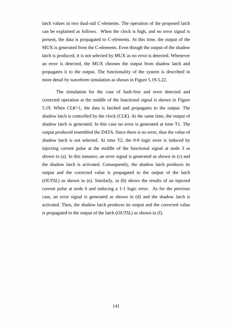
141
latch values in two dual-rail C-elements. The operation of the proposed latch
can be explained as follows. When the clock is high, and no error signal is
present, the data is propagated to C-elements. At this time, the output of the
MUX is generated from the C-elements. Even though the output of the shadow
latch is produced, it is not selected by MUX as no error is detected. Whenever
an error is detected, the MUX chooses the output from shadow latch and
propagates it to the output. The functionality of the system is described in
more detail by waveform simulation as shown in Figure 5.19-5.22.
The simulation for the case of fault-free and error detected and
corrected operation at the middle of the functional signal is shown in Figure
5.19. When CLK=1, the data is latched and propagates to the output. The
shadow latch is controlled by the clock (CLK). At the same time, the output of
shadow latch is generated. In this case no error is generated at time T1. The
output produced resembled the DATA. Since there is no error, thus the value of
shadow latch is not selected. At time T2, the 0-0 logic error is induced by
injecting current pulse at the middle of the functional signal at node 3 as
shown in (a). In this instance, an error signal is generated as shown in (c) and
the shadow latch is activated. Consequently, the shadow latch produces its
output and the corrected value is propagated to the output of the latch
(OUTSL) as shown in (e). Similarly, in (b) shows the results of an injected
current pulse at node 6 and inducing a 1-1 logic error. As for the previous
case, an error signal is generated as shown in (d) and the shadow latch is
activated. Then, the shadow latch produces its output and the corrected value
is propagated to the output of the latch (OUTSL) as shown in (f).

142
Figure 5.19: Fault Free, Error Detected and Error Corrected at the center of the
functional signal of for EDC Latch
The simulation is repeated for the case of error detected and corrected
operation at the edge of the functional signal as shown in Figure 5.20. At time
T2 illustrate node 3 is injecting with current pulse at the edge of the functional
signal causing the output of C-element 1 changing from 1 to 0 temporarily and
thus creating 0-0 error as shown in (a). The ERROR is high to indicate that
SEU error taking place at node 3 as shown in (c). The corrected output, OUT
due to 0-0 error is shown in (e).Similarly node 6 is injecting with current pulse
at the edge of the functional signal causing the output of C-element 2 changes
temporarily from 0 to 1 at time T3 and thus creating 1-1 error as shown in (b).
The ERROR is high to indicate that SEU error taking place at node 6 as shown
in (d). The corrected output, OUT due to 1-1 error is shown in (f)
DATA
CLK
Node3
Node6
ERROR
OUT
T1 T
2
T3
(a) (b)
(c) (d)
(e) (f)
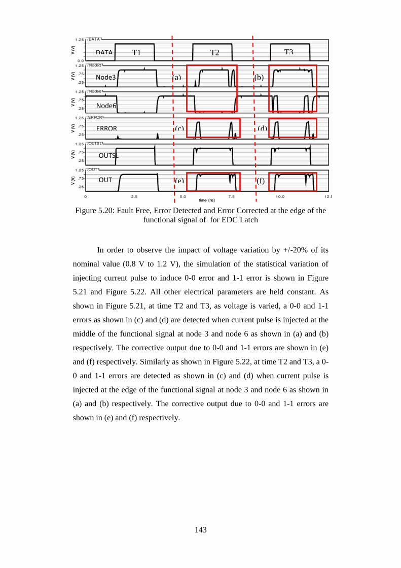
143
Figure 5.20: Fault Free, Error Detected and Error Corrected at the edge of the
functional signal of for EDC Latch
In order to observe the impact of voltage variation by +/-20% of its
nominal value (0.8 V to 1.2 V), the simulation of the statistical variation of
injecting current pulse to induce 0-0 error and 1-1 error is shown in Figure
5.21 and Figure 5.22. All other electrical parameters are held constant. As
shown in Figure 5.21, at time T2 and T3, as voltage is varied, a 0-0 and 1-1
errors as shown in (c) and (d) are detected when current pulse is injected at the
middle of the functional signal at node 3 and node 6 as shown in (a) and (b)
respectively. The corrective output due to 0-0 and 1-1 errors are shown in (e)
and (f) respectively. Similarly as shown in Figure 5.22, at time T2 and T3, a 0-
0 and 1-1 errors are detected as shown in (c) and (d) when current pulse is
injected at the edge of the functional signal at node 3 and node 6 as shown in
(a) and (b) respectively. The corrective output due to 0-0 and 1-1 errors are
shown in (e) and (f) respectively.
DATA
Node3
Node6
ERROR
OUTSL
OUT
T1 T2 T3
(a) (b)
(c) (d)
(e) (f)
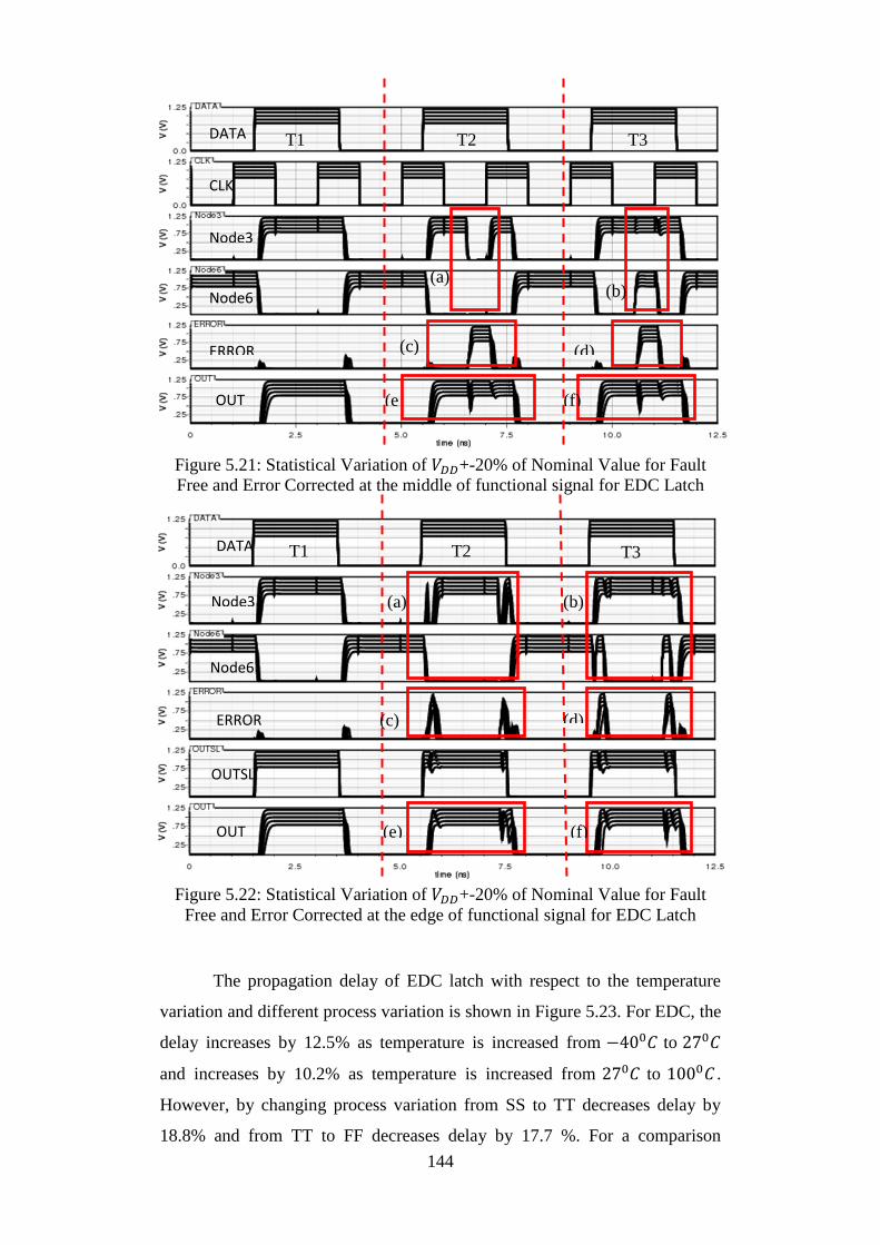
144
Figure 5.21: Statistical Variation of 𝑉𝐷𝐷+-20% of Nominal Value for Fault
Free and Error Corrected at the middle of functional signal for EDC Latch
Figure 5.22: Statistical Variation of 𝑉𝐷𝐷+-20% of Nominal Value for Fault
Free and Error Corrected at the edge of functional signal for EDC Latch
The propagation delay of EDC latch with respect to the temperature
variation and different process variation is shown in Figure 5.23. For EDC, the
delay increases by 12.5% as temperature is increased from −400𝐶 to 270𝐶
and increases by 10.2% as temperature is increased from 270𝐶 to 1000𝐶 .
However, by changing process variation from SS to TT decreases delay by
18.8% and from TT to FF decreases delay by 17.7 %. For a comparison
DATA
CLK
Node3
Node6
ERROR
OUT
T1 T2 T3
(a) (b)
(c) (d)
(e (f)
DATA
Node3
Node6
ERROR
OUTSL
OUT
T1 T2 T3
(a) (b)
(c) (d)
(e) (f)
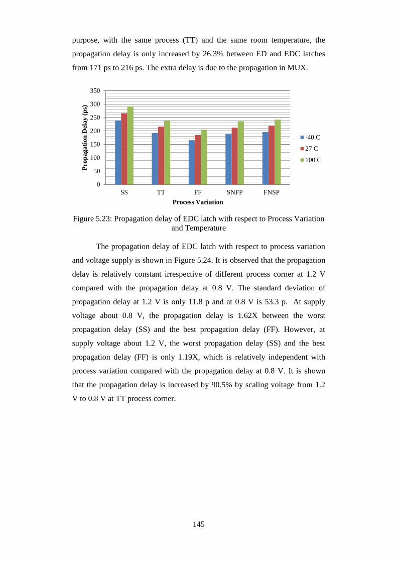
145
purpose, with the same process (TT) and the same room temperature, the
propagation delay is only increased by 26.3% between ED and EDC latches
from 171 ps to 216 ps. The extra delay is due to the propagation in MUX.
Figure 5.23: Propagation delay of EDC latch with respect to Process Variation
and Temperature
The propagation delay of EDC latch with respect to process variation
and voltage supply is shown in Figure 5.24. It is observed that the propagation
delay is relatively constant irrespective of different process corner at 1.2 V
compared with the propagation delay at 0.8 V. The standard deviation of
propagation delay at 1.2 V is only 11.8 p and at 0.8 V is 53.3 p. At supply
voltage about 0.8 V, the propagation delay is 1.62X between the worst
propagation delay (SS) and the best propagation delay (FF). However, at
supply voltage about 1.2 V, the worst propagation delay (SS) and the best
propagation delay (FF) is only 1.19X, which is relatively independent with
process variation compared with the propagation delay at 0.8 V. It is shown
that the propagation delay is increased by 90.5% by scaling voltage from 1.2
V to 0.8 V at TT process corner.
0
50
100
150
200
250
300
350
SS TT FF SNFP FNSP
Pro
pa
ga
tio
n D
ela
y (
ps)
Process Variation
-40 C
27 C
100 C
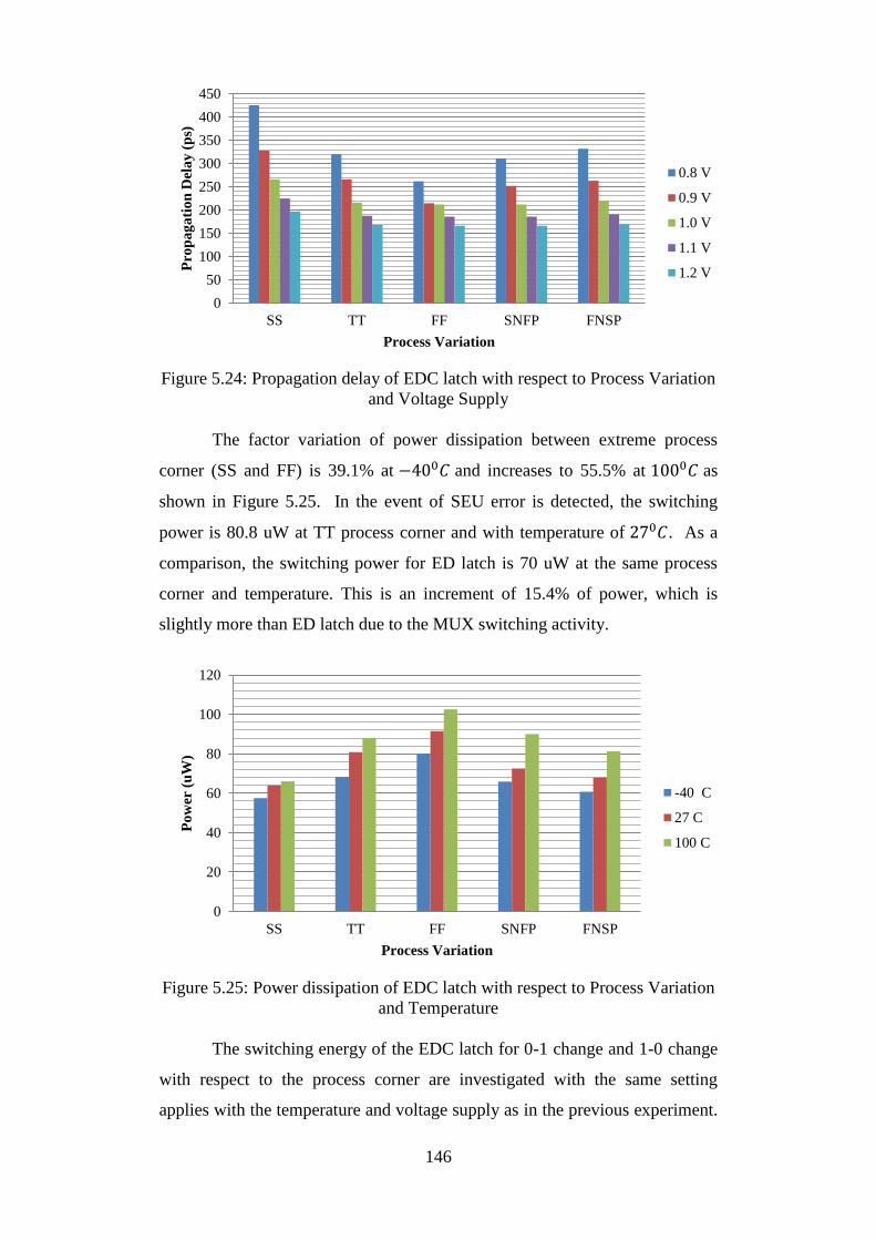
146
Figure 5.24: Propagation delay of EDC latch with respect to Process Variation
and Voltage Supply
The factor variation of power dissipation between extreme process
corner (SS and FF) is 39.1% at −400𝐶 and increases to 55.5% at 1000𝐶 as
shown in Figure 5.25. In the event of SEU error is detected, the switching
power is 80.8 uW at TT process corner and with temperature of 270𝐶. As a
comparison, the switching power for ED latch is 70 uW at the same process
corner and temperature. This is an increment of 15.4% of power, which is
slightly more than ED latch due to the MUX switching activity.
Figure 5.25: Power dissipation of EDC latch with respect to Process Variation
and Temperature
The switching energy of the EDC latch for 0-1 change and 1-0 change
with respect to the process corner are investigated with the same setting
applies with the temperature and voltage supply as in the previous experiment.
0
50
100
150
200
250
300
350
400
450
SS TT FF SNFP FNSP
Pro
pa
ga
tio
n D
ela
y (
ps)
Process Variation
0.8 V
0.9 V
1.0 V
1.1 V
1.2 V
0
20
40
60
80
100
120
SS TT FF SNFP FNSP
Po
wer
(u
W)
Process Variation
-40 C
27 C
100 C

147
From Figure 5.26 and 5.27, it is shown that the process corner of SS, TT and
FF have identical critical charge with ED latch for 0-1 change and 1-0 change.
For 0-1 change, SS has the lowest maximum switching energy (106 fJ)
compared with TT (119 fJ) and FF (134 fJ). The switching energy for FF is
1.26X compared with SS. Similarly, for 1-0 change SS has the lowest
maximum switching energy (68 fJ) compared with TT (81 fJ) and FF (28 fJ).
The switching energy for FF is 1.4X compared with SS. For the same process
corner, TT, the maximum switching energy for EDC latch is 19% higher
compared with the maximum switching energy for ED latch. The latch has the
initial switching energy values of 26 fJ (SS), 28 fJ (TT) and 30 fJ (FF)
corresponding to the no current pulse injected into the node.
Figure 5.26: Switching Energy for EDC Latch (0-1 Change) with Different
Process Variation
Figure 5.27: Switching Energy for EDC Latch (1-0 Change) with Different
Process Variation
0
20
40
60
80
100
120
140
0 10 20 30 40
Sw
itch
ing
En
erg
y (
fJ)
SEU Charge (fC)
SS
TT
FF
0
10
20
30
40
50
60
70
80
90
100
46.8 51.8 56.8 61.8 66.8 71.8 76.8
Sw
itch
ing
En
erg
y (
fJ)
SEU Charge
SS
TT
FF
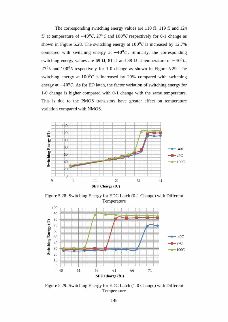
148
The corresponding switching energy values are 110 fJ, 119 fJ and 124
fJ at temperature of −400𝐶, 270𝐶 and 1000𝐶 respectively for 0-1 change as
shown in Figure 5.28. The switching energy at 1000𝐶 is increased by 12.7%
compared with switching energy at −400𝐶 . Similarly, the corresponding
switching energy values are 69 fJ, 81 fJ and 88 fJ at temperature of −400𝐶,
270𝐶 and 1000𝐶 respectively for 1-0 change as shown in Figure 5.29. The
switching energy at 1000𝐶 is increased by 29% compared with switching
energy at −400𝐶. As for ED latch, the factor variation of switching energy for
1-0 change is higher compared with 0-1 change with the same temperature.
This is due to the PMOS transistors have greater effect on temperature
variation compared with NMOS.
Figure 5.28: Switching Energy for EDC Latch (0-1 Change) with Different
Temperature
Figure 5.29: Switching Energy for EDC Latch (1-0 Change) with Different
Temperature
0
20
40
60
80
100
120
140
-9 1 11 21 31 41
Sw
itch
ing
En
erg
y (
fJ)
SEU Charge (fC)
-40C
27C
100C
0
10
20
30
40
50
60
70
80
90
100
46 51 56 61 66 71
Sw
itch
ing
En
erg
y (
fJ)
SEU Charge (fC)
-40C
27C
100C
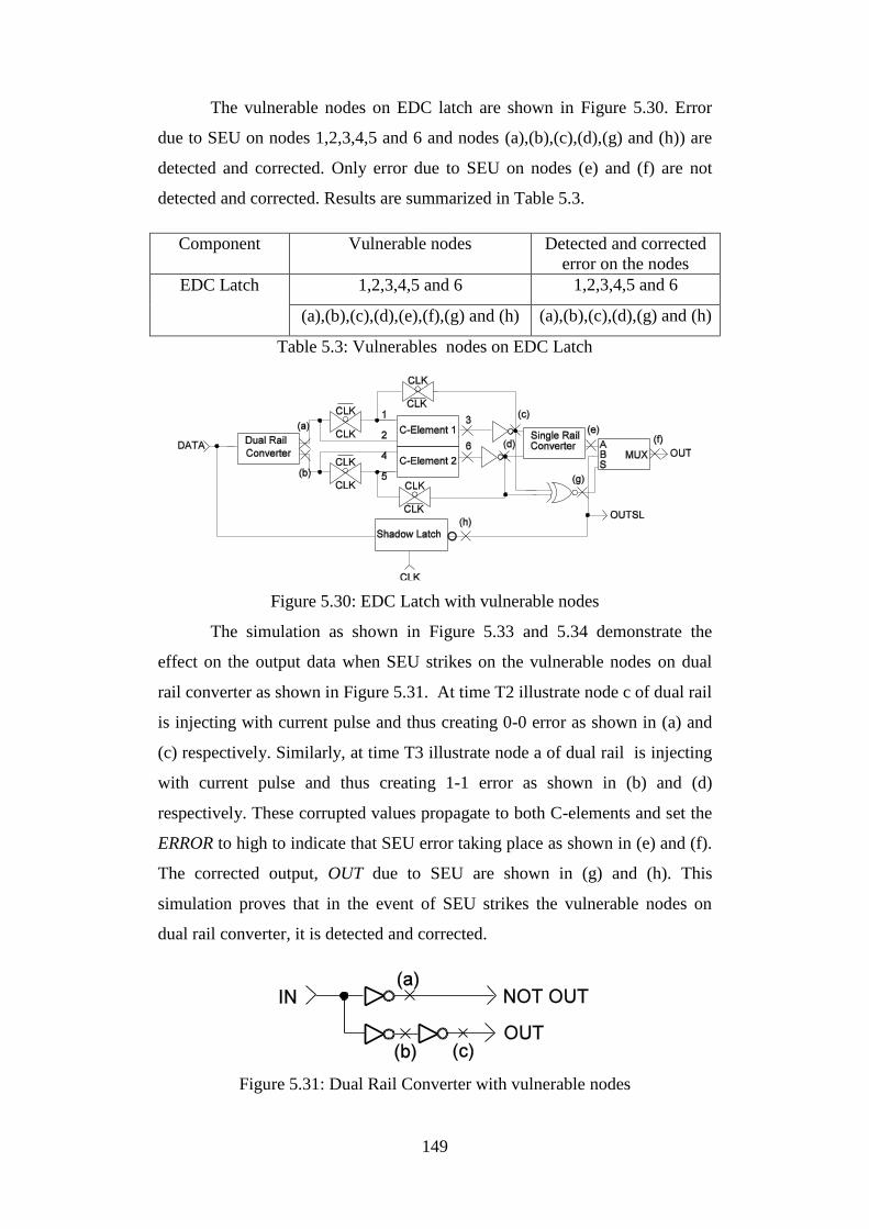
149
The vulnerable nodes on EDC latch are shown in Figure 5.30. Error
due to SEU on nodes 1,2,3,4,5 and 6 and nodes (a),(b),(c),(d),(g) and (h)) are
detected and corrected. Only error due to SEU on nodes (e) and (f) are not
detected and corrected. Results are summarized in Table 5.3.
Component Vulnerable nodes Detected and corrected
error on the nodes
EDC Latch 1,2,3,4,5 and 6 1,2,3,4,5 and 6
(a),(b),(c),(d),(e),(f),(g) and (h) (a),(b),(c),(d),(g) and (h)
Table 5.3: Vulnerables nodes on EDC Latch
Figure 5.30: EDC Latch with vulnerable nodes
The simulation as shown in Figure 5.33 and 5.34 demonstrate the
effect on the output data when SEU strikes on the vulnerable nodes on dual
rail converter as shown in Figure 5.31. At time T2 illustrate node c of dual rail
is injecting with current pulse and thus creating 0-0 error as shown in (a) and
(c) respectively. Similarly, at time T3 illustrate node a of dual rail is injecting
with current pulse and thus creating 1-1 error as shown in (b) and (d)
respectively. These corrupted values propagate to both C-elements and set the
ERROR to high to indicate that SEU error taking place as shown in (e) and (f).
The corrected output, OUT due to SEU are shown in (g) and (h). This
simulation proves that in the event of SEU strikes the vulnerable nodes on
dual rail converter, it is detected and corrected.
Figure 5.31: Dual Rail Converter with vulnerable nodes

150
Figure 5.32: Single Rail Converter with vulnerable nodes
Figure 5.33: Error injected to Dual Rail Converter
Figure 5.34: Corrected error due to the injected error to Dual Rail Converter
The simulation in Figure 5.35 demonstrates the effect on the output
data when SEU strikes on the vulnerable nodes on shadow latches(node h) and
XNOR gate (node g) of Figure 5.30. If the SEU strikes on shadow latch as
shown in (a), this value is not selected because the ERROR is still low. If SEU
A
NOT
Node 3
Node 6
T1 T2 T3 (a) (b
)
(c) (d)
DATA
CLK
ERROR
OUT
T1 T2 T3
(e) (f)
(g) (h)
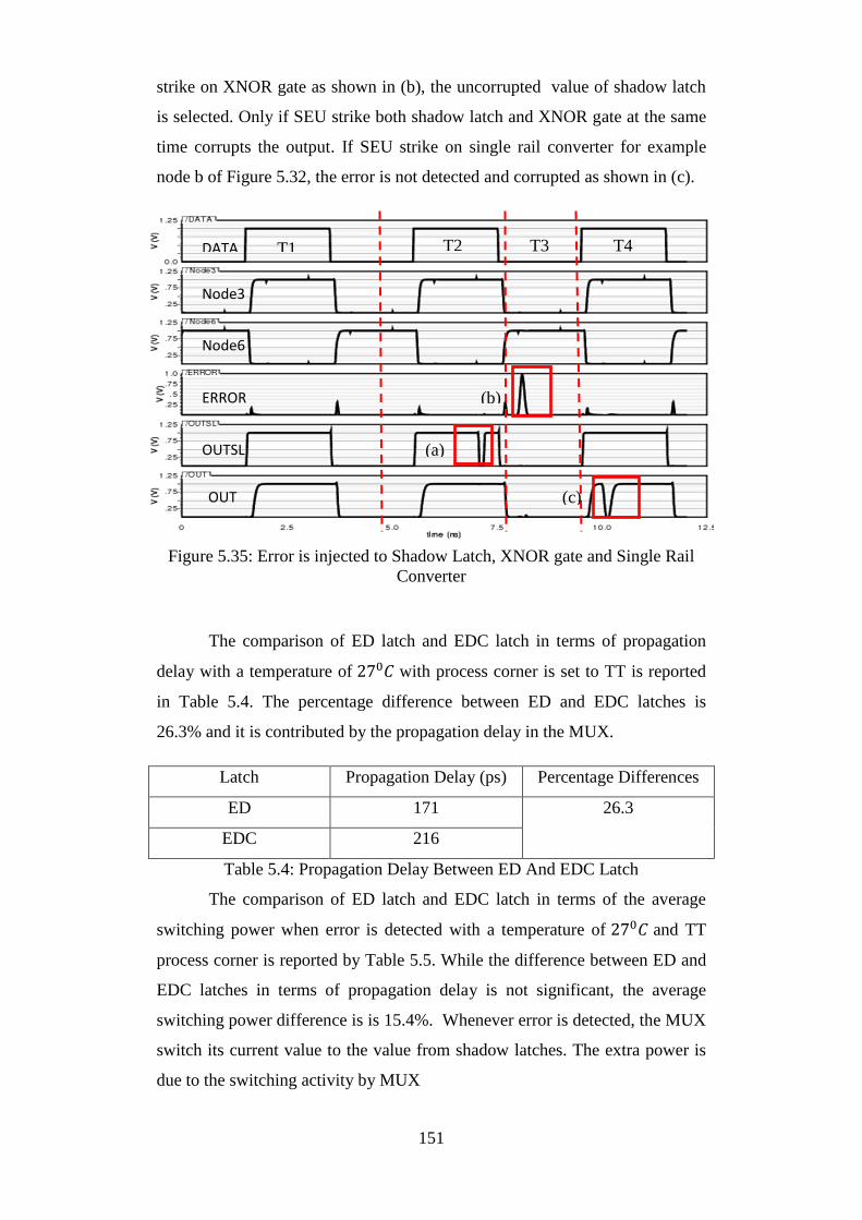
151
strike on XNOR gate as shown in (b), the uncorrupted value of shadow latch
is selected. Only if SEU strike both shadow latch and XNOR gate at the same
time corrupts the output. If SEU strike on single rail converter for example
node b of Figure 5.32, the error is not detected and corrupted as shown in (c).
Figure 5.35: Error is injected to Shadow Latch, XNOR gate and Single Rail
Converter
The comparison of ED latch and EDC latch in terms of propagation
delay with a temperature of 270𝐶 with process corner is set to TT is reported
in Table 5.4. The percentage difference between ED and EDC latches is
26.3% and it is contributed by the propagation delay in the MUX.
Latch Propagation Delay (ps) Percentage Differences
ED 171 26.3
EDC 216
Table 5.4: Propagation Delay Between ED And EDC Latch
The comparison of ED latch and EDC latch in terms of the average
switching power when error is detected with a temperature of 270𝐶 and TT
process corner is reported by Table 5.5. While the difference between ED and
EDC latches in terms of propagation delay is not significant, the average
switching power difference is is 15.4%. Whenever error is detected, the MUX
switch its current value to the value from shadow latches. The extra power is
due to the switching activity by MUX
DATA
Node3
Node6
ERROR
OUTSL
OUT
T1 T2 T3 T4
(b)
(a)
(c)
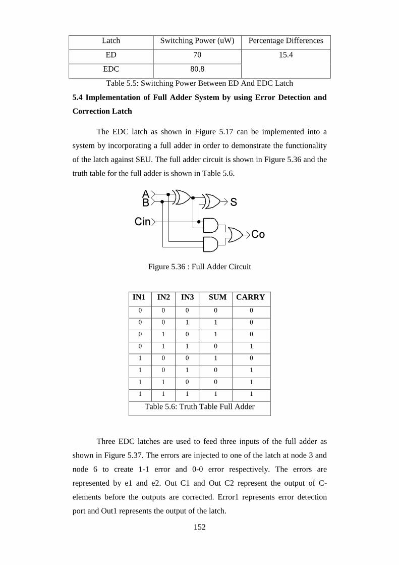
152
Latch Switching Power (uW) Percentage Differences
ED 70 15.4
EDC 80.8
Table 5.5: Switching Power Between ED And EDC Latch
5.4 Implementation of Full Adder System by using Error Detection and
Correction Latch
The EDC latch as shown in Figure 5.17 can be implemented into a
system by incorporating a full adder in order to demonstrate the functionality
of the latch against SEU. The full adder circuit is shown in Figure 5.36 and the
truth table for the full adder is shown in Table 5.6.
Figure 5.36 : Full Adder Circuit
IN1 IN2 IN3 SUM CARRY
0 0 0 0 0
0 0 1 1 0
0 1 0 1 0
0 1 1 0 1
1 0 0 1 0
1 0 1 0 1
1 1 0 0 1
1 1 1 1 1
Table 5.6: Truth Table Full Adder
Three EDC latches are used to feed three inputs of the full adder as
shown in Figure 5.37. The errors are injected to one of the latch at node 3 and
node 6 to create 1-1 error and 0-0 error respectively. The errors are
represented by e1 and e2. Out C1 and Out C2 represent the output of C-
elements before the outputs are corrected. Error1 represents error detection
port and Out1 represents the output of the latch.
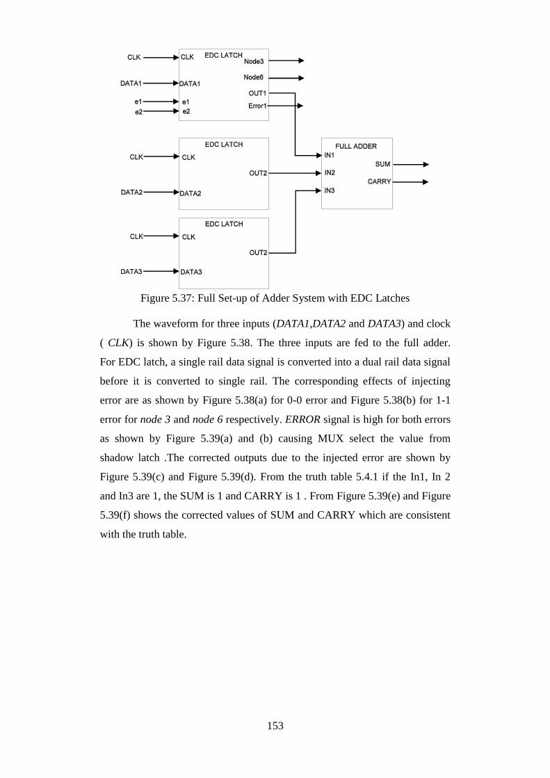
153
Figure 5.37: Full Set-up of Adder System with EDC Latches
The waveform for three inputs (DATA1,DATA2 and DATA3) and clock
( CLK) is shown by Figure 5.38. The three inputs are fed to the full adder.
For EDC latch, a single rail data signal is converted into a dual rail data signal
before it is converted to single rail. The corresponding effects of injecting
error are as shown by Figure 5.38(a) for 0-0 error and Figure 5.38(b) for 1-1
error for node 3 and node 6 respectively. ERROR signal is high for both errors
as shown by Figure 5.39(a) and (b) causing MUX select the value from
shadow latch .The corrected outputs due to the injected error are shown by
Figure 5.39(c) and Figure 5.39(d). From the truth table 5.4.1 if the In1, In 2
and In3 are 1, the SUM is 1 and CARRY is 1 . From Figure 5.39(e) and Figure
5.39(f) shows the corrected values of SUM and CARRY which are consistent
with the truth table.
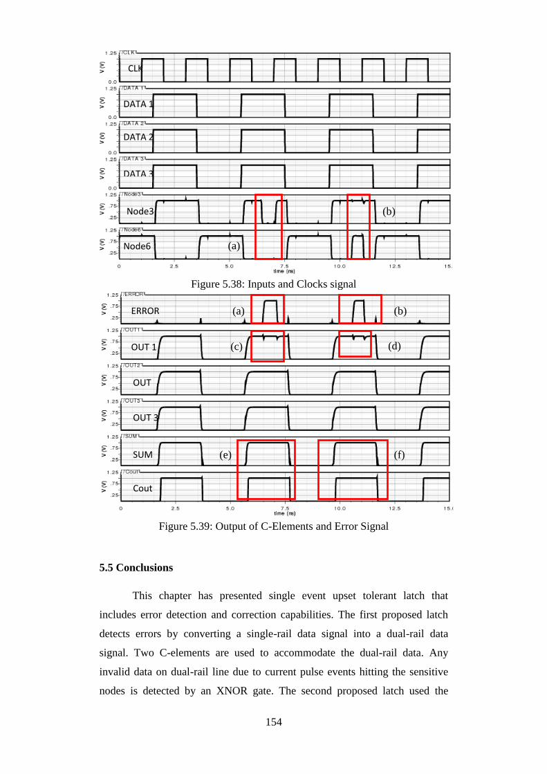
154
Figure 5.38: Inputs and Clocks signal
Figure 5.39: Output of C-Elements and Error Signal
5.5 Conclusions
This chapter has presented single event upset tolerant latch that
includes error detection and correction capabilities. The first proposed latch
detects errors by converting a single-rail data signal into a dual-rail data
signal. Two C-elements are used to accommodate the dual-rail data. Any
invalid data on dual-rail line due to current pulse events hitting the sensitive
nodes is detected by an XNOR gate. The second proposed latch used the
CLK
DATA 1
DATA 2
DATA 3
Node3
Node6 (a)
(b)
ERROR
OUT 1
OUT
2
OUT 3
SUM
Cout
(a) (b)
(c) (d)
(e) (f)

155
concept of Razor flip-flop to correct errors by employing a shadow latch that
is controlled by the same clock in order to restore correct values. By using
Cadence UMC 90nm, the functionality of both ED and EDC latches are
demonstrated by using waveforms under fault free condition and in the event
of current pulse hits the vulnerable nodes. The performance of ED and EDC
latches latch are analysed in terms of propagation delay versus process corner,
temperature and voltage supply. It is concluded that ED latch is 26.3% faster
than EDC latch and EDC latch consumes 15.4% more power compared with
ED latch. The relation of current charge with respect to switching energy of
both latches with different process corner and temperature are also obtained.
The functionality of the latches are also tested by incorporating a full adder in
the system and it is concluded the latches works as expected.
156
Chapter 6. Error Detection and Correction of Single Event
Upset Tolerant Latch for Dual Rail Data
This chapter presents error detection for a dual rail latch (EDD and error
detection and correction for dual rail latch (EDCD)). The functionality of both
EDD and EDCD latches are demonstrated using Cadence UMC 90nm. The
waveforms under fault free conditions and in the event of SEU striking the
vulnerable nodes are obtained. The performance of EDD and EDCD latches
are analysed in terms of propagation delay and switching power. The error
detection and correction with transient error correction latch (EDCDT) is also
proposed in this chapter.
6.1 Introduction
In globally asynchronous locally synchronous (GALS) design, single
rail data which utilise N lines to represent N bit of information is the most
common data representation in asynchronous communication [62]. However,
this type of representation has disadvantage: The single rail is subjected to
delay variation sensitive. It has timing constraint between the control signal
and data and hence does not suitable for long on-chip communication [62].
Dual rail encoding is necessary for long on-chip interconnect since it is delay
insensitive which refers to the data is transmitted correctly regardless of the
delay in the interconnecting wires. It uses two wires to represent 1 bit of
information.
In this chapter, three types of latches for dual rail data are proposed to
mitigate the effect of single event upset (SEU) and single event transient
(SET) on dual rail data.
a) Error detection for dual rail data (EDD)
b) Error detection and correction for dual rail data (EDCD)
c) Error detection and correction with transient correction for dual rail
(EDCDT)
6.2 Proposed Error Detection for Dual Rail Data
The ED and EDC latches as proposed in Chapter 5 for single rail data
latches suffer two main problems. The propagation delay of ED and EDC
latches are quite significant due to the converters. The use of ED and EDC for
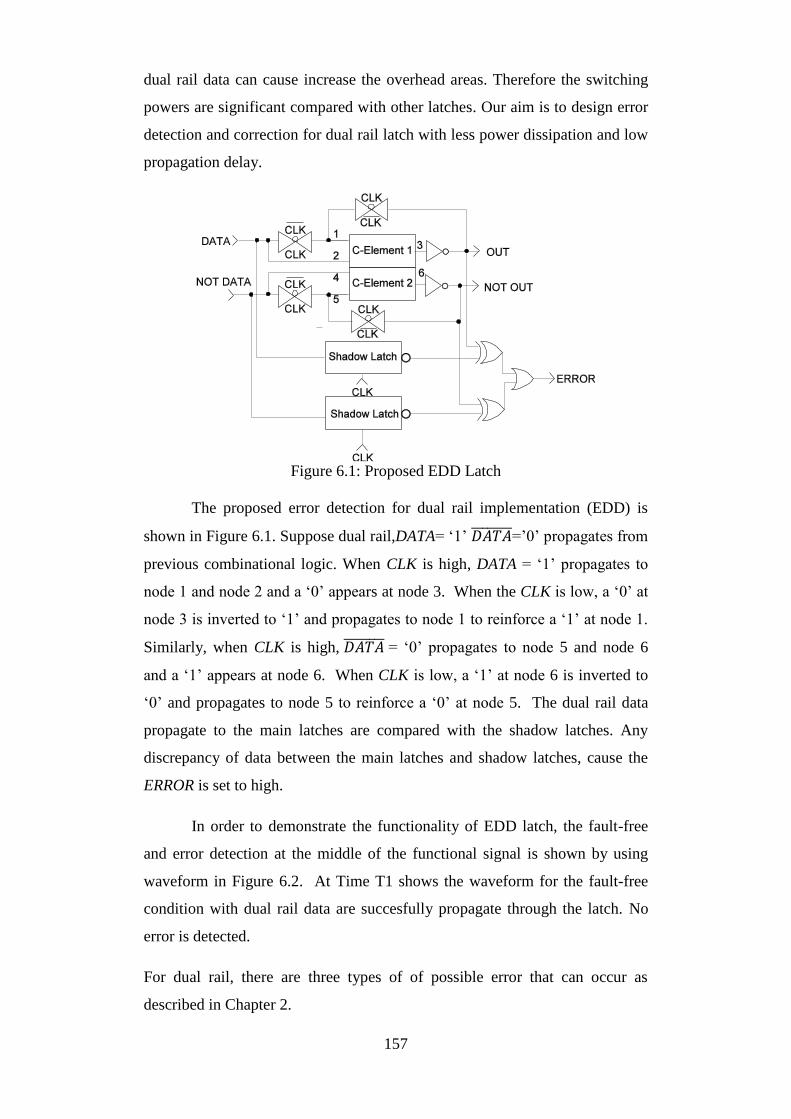
157
dual rail data can cause increase the overhead areas. Therefore the switching
powers are significant compared with other latches. Our aim is to design error
detection and correction for dual rail latch with less power dissipation and low
propagation delay.
Figure 6.1: Proposed EDD Latch
The proposed error detection for dual rail implementation (EDD) is
shown in Figure 6.1. Suppose dual rail,DATA= ‘1’ 𝐷𝐴𝑇𝐴̅̅ ̅̅ ̅̅ ̅̅ =’0’ propagates from
previous combinational logic. When CLK is high, DATA = ‘1’ propagates to
node 1 and node 2 and a ‘0’ appears at node 3. When the CLK is low, a ‘0’ at
node 3 is inverted to ‘1’ and propagates to node 1 to reinforce a ‘1’ at node 1.
Similarly, when CLK is high, 𝐷𝐴𝑇𝐴̅̅ ̅̅ ̅̅ ̅̅ = ‘0’ propagates to node 5 and node 6
and a ‘1’ appears at node 6. When CLK is low, a ‘1’ at node 6 is inverted to
‘0’ and propagates to node 5 to reinforce a ‘0’ at node 5. The dual rail data
propagate to the main latches are compared with the shadow latches. Any
discrepancy of data between the main latches and shadow latches, cause the
ERROR is set to high.
In order to demonstrate the functionality of EDD latch, the fault-free
and error detection at the middle of the functional signal is shown by using
waveform in Figure 6.2. At Time T1 shows the waveform for the fault-free
condition with dual rail data are succesfully propagate through the latch. No
error is detected.
For dual rail, there are three types of of possible error that can occur as
described in Chapter 2.

158
(a) Data generation: Error on Spacer that can cause 01 or 10 error.
(b) Data generation: 1-1 error on valid data.
(c) Data vanishing: 0-0 error on valid data.
At time T2, the current pulse is injected at node 3 and results in the
output of C-element 1 changing from 1 to 0 temporarily as shown in (a). Node
6 remains undisturbed. As a result, this causes a 0-0 error. Similarly, at time
T3 the current pulse is injected at node 6 and results in the output of C-
element 2 changing from 0 to 1 temporarily. This causes a spacer error and
this data is considered invalid as shown in (b). At time T4 current pulse is
injected at node 6 and results in the output of C-element 2 changing from 0 to
1 temporarily. Node 3 remains undisturbed. As a result, this causes a 1-1 error
and this data is considered invalid as shown in (c). For all the casses, error are
detected as shown by ERROR.
The simulation is repeated for the case of error detected operation at
the edge of the functional signal as shown in Figure 6.3. At time T2 illustrate
node 3 is injecting with current pulse at the edge of the functional signal
causing the output of C-element 1 changing from 1 to 0 temporarily and thus
creating 0-0 error as shown in (a).Similarly node 6 is injecting with current
pulse at the edge of the functional signal causing the output of C-element 2
changes temporarily from 0 to 1 at time T3 and thus creating 1-1 error as
shown in (b). For 0-0 error and 1-1 error, the ERROR is high to indicate that
SEU error taking place at node 3 and node 6 of C-elements respectively.

159
Figure 6.2: Fault-free and Error Detected at the middle of the functional signal
for EDD Latch
Figure 6.3: Fault-free and Error Detected at the edge of the functional signal
for EDD Latch
The experiment is repeated for EDD in order to observe the impact of
voltage variation by +/-20% of its nominal value (0.8 V to 1.2 V). Figure 6.4
shows the simulation of the statistical variation of injecting current pulse
induce 0-0, spacer and 1-1errors as shown in (a),(b) and (c) respectively. All
other electrical parameters are held constant.
DATA
NOT
CLK
ERROR
NOT OUT
OUT
T1 T2 T3 T4
(a) (b) (c)
DATA
NOT DATA
CLK
ERROR
NOT OUT
OUT
T1 T2 T3
(a) (b)
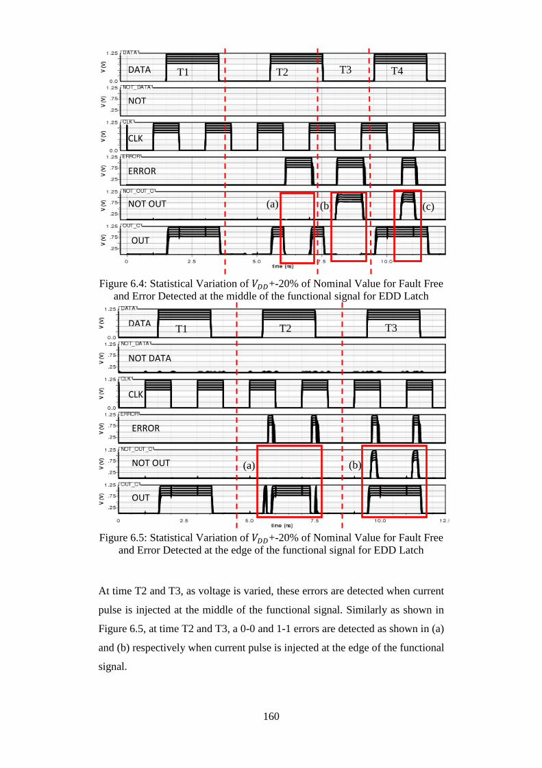
160
Figure 6.4: Statistical Variation of 𝑉𝐷𝐷+-20% of Nominal Value for Fault Free
and Error Detected at the middle of the functional signal for EDD Latch
Figure 6.5: Statistical Variation of 𝑉𝐷𝐷+-20% of Nominal Value for Fault Free
and Error Detected at the edge of the functional signal for EDD Latch
At time T2 and T3, as voltage is varied, these errors are detected when current
pulse is injected at the middle of the functional signal. Similarly as shown in
Figure 6.5, at time T2 and T3, a 0-0 and 1-1 errors are detected as shown in (a)
and (b) respectively when current pulse is injected at the edge of the functional
signal.
DATA
NOT
CLK
ERROR
NOT OUT
OUT
T1 T2 T3 T4
(a) (b) (c)
DATA
NOT DATA
CLK
ERROR
NOT OUT
OUT
T1 T2 T3
(a) (b)

161
In order to investigate the propagation delay of EDD latch with respect
to the temperature variation and different process variation the experiment is
conducted and the result is shown in Figure 6.6. As before, three different
temperatures are under consideration in our analysis. For EDD, the delay
increases by 14.8% as temperature is increased from −400𝐶 to 270𝐶 and
increases by 11.6% as temperature is increased from 270𝐶 to 1000𝐶 .
However, by changing process variation from SS to TT decreases delay by
24.5% and from TT to FF decreases delay by 20.4 %. For a comparison
purpose, with the same process (TT) and room temperature, the propagation
delay for ED latch is 4X longer compared with EDD latch. This huge
difference is mainly due to the delay in the converters in ED latch. However,
one problem exist in EDD latch is that the DATA propagate faster than the
error signal due to the logic gate needed to detect the presence of the signal.
This could cause problem as the error due to SEU propagate to the output
before it is corrected as the error signal propagate slower. In order to solve this
problem, the appropriate delays are inserted to allow the error signal propagate
faster than the output so the correction mechanism of SEU works. This is
discussed in Section 6.3.
Figure 6.6: Propagation delay of EDD latch with respect to Process Variation
and Temperature
The propagation delay of EDD latch with respect to process variation
and voltage supply are also measured. Figure 6.7 reports the result. At supply
voltage about 0.8 V, the propagation delay is 1.9X between the worst
propagation delay (SS) and the best propagation delay (FF). However, at
0
10
20
30
40
50
60
70
SS TT FF SNFP FNSP
Pro
pa
ga
tio
n D
ela
y (
ps)
Process Variation
-40 C
27 C
100 C
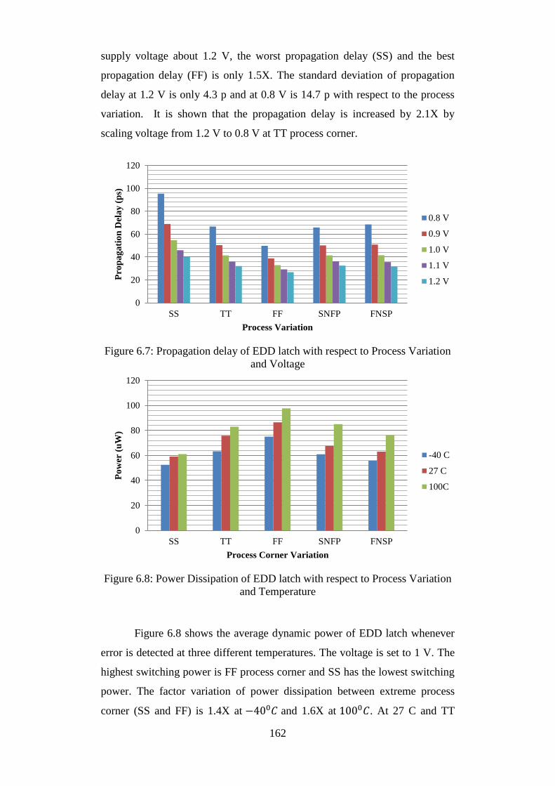
162
supply voltage about 1.2 V, the worst propagation delay (SS) and the best
propagation delay (FF) is only 1.5X. The standard deviation of propagation
delay at 1.2 V is only 4.3 p and at 0.8 V is 14.7 p with respect to the process
variation. It is shown that the propagation delay is increased by 2.1X by
scaling voltage from 1.2 V to 0.8 V at TT process corner.
Figure 6.7: Propagation delay of EDD latch with respect to Process Variation
and Voltage
Figure 6.8: Power Dissipation of EDD latch with respect to Process Variation
and Temperature
Figure 6.8 shows the average dynamic power of EDD latch whenever
error is detected at three different temperatures. The voltage is set to 1 V. The
highest switching power is FF process corner and SS has the lowest switching
power. The factor variation of power dissipation between extreme process
corner (SS and FF) is 1.4X at −400𝐶 and 1.6X at 1000𝐶. At 27 C and TT
0
20
40
60
80
100
120
SS TT FF SNFP FNSP
Pro
pa
ga
tio
n D
ela
y (
ps)
Process Variation
0.8 V
0.9 V
1.0 V
1.1 V
1.2 V
0
20
40
60
80
100
120
SS TT FF SNFP FNSP
Po
wer
(u
W)
Process Corner Variation
-40 C
27 C
100C
163
process corner, the average dynamic power is 76 µW whenever error is
detected.
The switching energy of the EDD latch for 0-1 change and for 1-0
change are shown in Figure 6.9 and 6.10 respectively. It is observed that the
process corner of SS, TT and FF have identical critical charge with ED latch
for 0-1 change and 1-0 change. For 0-1 change, SS has the lowest maximum
switching energy (102 fJ) compared with TT (112 fJ) and FF (129 fJ). The
switching energy for FF is 1.26X compared with SS. As a comparison with
ED latch, in the event of SEU is detected and caused the state to change, at
TT process corner, EDD latch is 3% higher of switching energy compared
with ED latch for 0-1 change Similarly, for 1-0 change SS has the lowest
maximum switching energy (69 fJ) compared with TT (72 fJ) and FF (83 fJ).
The above experiments are repeated at three different temperatures as
shown in Figure 6.11 and Figure 6.12. The corresponding switching energy
values are 105 fJ, 112 fJ and 120 fJ for at temperature of −400𝐶, 270𝐶 and
1000𝐶 respectively for 0-1 change. The switching energy at 1000𝐶 is 15.2%
higher compared with switching energy at −400𝐶 . Similarly, the
corresponding switching energy values are 67 fJ, 72 fJ and 78 fJ at
temperature of −400𝐶 , 270𝐶 and 1000𝐶 respectively for 1-0 change. The
switching energy at 1000𝐶 is 16.4% higher compared with switching energy
at −400𝐶 . As for ED and EDC latch, the percentage change of switching
energy for 1-0 change between temperature at −400𝐶 and 1000𝐶 is higher
compared with 0-1 change with the same temperature.
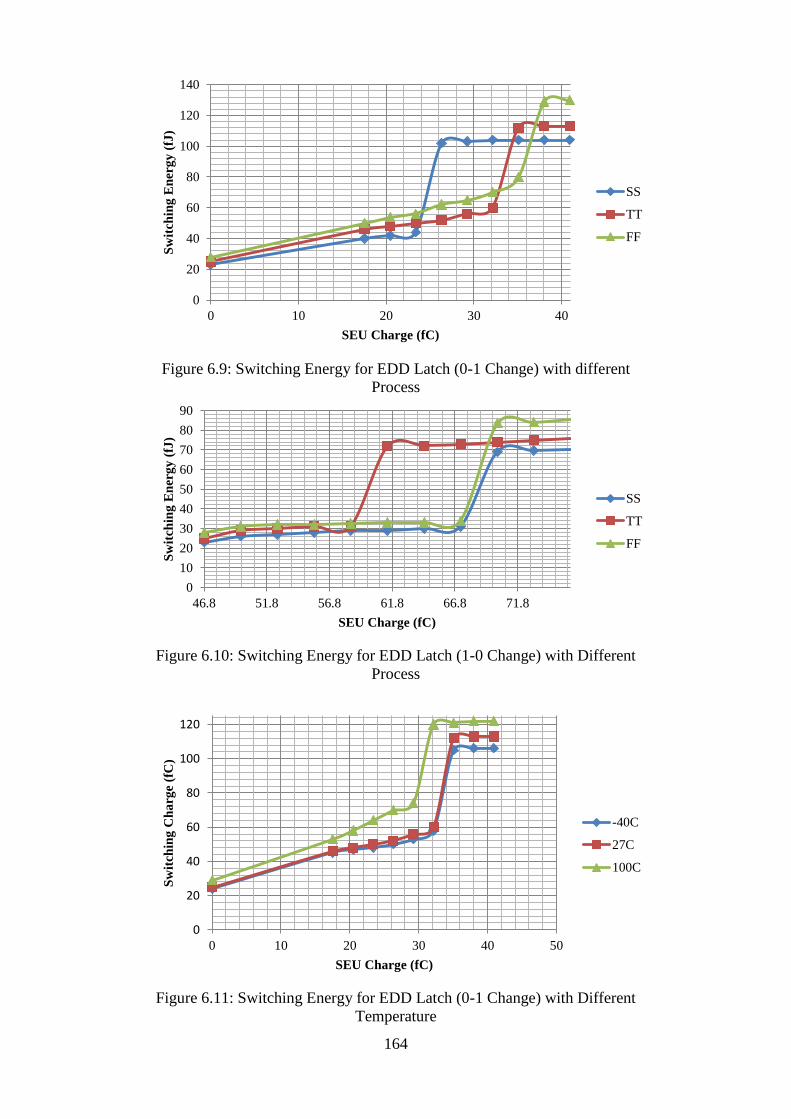
164
Figure 6.9: Switching Energy for EDD Latch (0-1 Change) with different
Process
Figure 6.10: Switching Energy for EDD Latch (1-0 Change) with Different
Process
Figure 6.11: Switching Energy for EDD Latch (0-1 Change) with Different
Temperature
0
20
40
60
80
100
120
140
0 10 20 30 40
Sw
itch
ing
En
erg
y (
fJ)
SEU Charge (fC)
SS
TT
FF
0
10
20
30
40
50
60
70
80
90
46.8 51.8 56.8 61.8 66.8 71.8
Sw
itch
ing
En
erg
y (
fJ)
SEU Charge (fC)
SS
TT
FF
0
20
40
60
80
100
120
0 10 20 30 40 50
Sw
itch
ing
Ch
arg
e (f
C)
SEU Charge (fC)
-40C
27C
100C

165
Figure 6.12: Switching Energy for EDD Latch (1-0 Change) with Different
Temperature
The vulnerable nodes on EDD latch are shown in Figure 6.13. Error on nodes
1,2,3,4,5 and 6 and nodes (a),(b),(c) and (d) are detectable if there is error on
the nodes due to SEU. However if there SEU error on node (e),(f) and (g), it
only generate error without changing the output. Results are summarized in
Table 6.1.
Component Vulnerable nodes Detected error on the
nodes
EDD Latch 1,2,3,4,5 and 6 1,2,3,4,5 and 6
(a),(b),(c),(d),(e),(f) and
(g)
(a),(b),(c) and (d)
Table 6.1: Vulnerable nodes on EDD Latch
Figure 6.13: Vulnerable nodes on EDD Latch
0
10
20
30
40
50
60
70
80
46.7 51.7 56.7 61.7 66.7 71.7
Sw
itch
ing
En
erg
y (
fJ)
SEU Charge (fC)
-40C
27C
100C
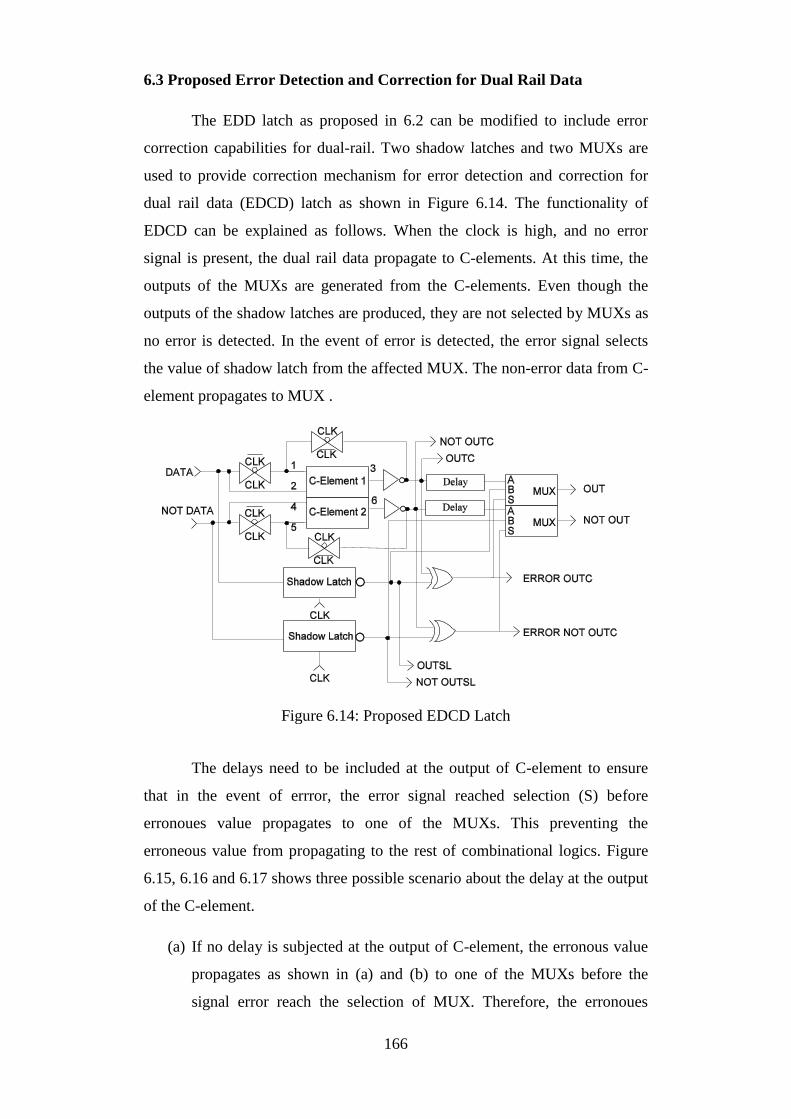
166
6.3 Proposed Error Detection and Correction for Dual Rail Data
The EDD latch as proposed in 6.2 can be modified to include error
correction capabilities for dual-rail. Two shadow latches and two MUXs are
used to provide correction mechanism for error detection and correction for
dual rail data (EDCD) latch as shown in Figure 6.14. The functionality of
EDCD can be explained as follows. When the clock is high, and no error
signal is present, the dual rail data propagate to C-elements. At this time, the
outputs of the MUXs are generated from the C-elements. Even though the
outputs of the shadow latches are produced, they are not selected by MUXs as
no error is detected. In the event of error is detected, the error signal selects
the value of shadow latch from the affected MUX. The non-error data from C-
element propagates to MUX .
Figure 6.14: Proposed EDCD Latch
The delays need to be included at the output of C-element to ensure
that in the event of errror, the error signal reached selection (S) before
erronoues value propagates to one of the MUXs. This preventing the
erroneous value from propagating to the rest of combinational logics. Figure
6.15, 6.16 and 6.17 shows three possible scenario about the delay at the output
of the C-element.
(a) If no delay is subjected at the output of C-element, the erronous value
propagates as shown in (a) and (b) to one of the MUXs before the
signal error reach the selection of MUX. Therefore, the erronoues
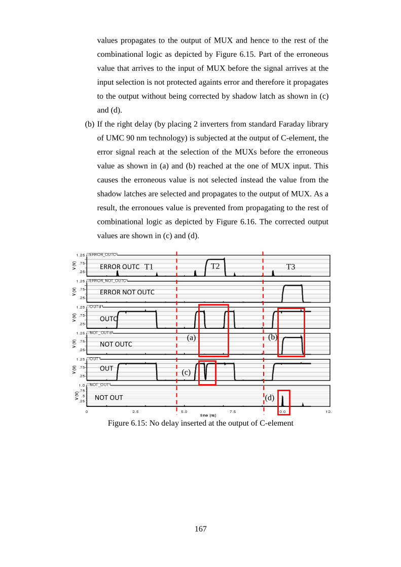
167
values propagates to the output of MUX and hence to the rest of the
combinational logic as depicted by Figure 6.15. Part of the erroneous
value that arrives to the input of MUX before the signal arrives at the
input selection is not protected againts error and therefore it propagates
to the output without being corrected by shadow latch as shown in (c)
and (d).
(b) If the right delay (by placing 2 inverters from standard Faraday library
of UMC 90 nm technology) is subjected at the output of C-element, the
error signal reach at the selection of the MUXs before the erroneous
value as shown in (a) and (b) reached at the one of MUX input. This
causes the erroneous value is not selected instead the value from the
shadow latches are selected and propagates to the output of MUX. As a
result, the erronoues value is prevented from propagating to the rest of
combinational logic as depicted by Figure 6.16. The corrected output
values are shown in (c) and (d).
Figure 6.15: No delay inserted at the output of C-element
T1 T2 T3
(a) (b)
(c)
(d) NOT OUT
OUT
NOT OUTC
OUTC
ERROR NOT OUTC
ERROR OUTC

168
Figure 6.16: Correct delay inserted at the output of C-element
(c) If the delay is subjected at the output of C-element and the delay is
longer than the error signal (by placing 4 inverters from standard
Faraday library of UMC 90 nm technology) causing error signal
propagates to the output before the erroneous value reached to one of
the MUXs input.
Figure 6.17: Delay is longer than error signal pulse
This results in the erroneous value as shown in (a) and (b) propagates to the
output of MUX as depicted by Figure 6.17. The corrected outputs due to the
T
1 T2 T3
(a) (b)
(c)
(d)
ERROR OUTC
ERROR NOT OUTC
OUTC
NOT OUTC
OUT
NOT OUT
T1 T2 T3
(a) (b)
(c)
(d)
ERROR OUTC
ERROR NOT OUTC
OUTC
NOT OUTC
OUT
NOT OUT
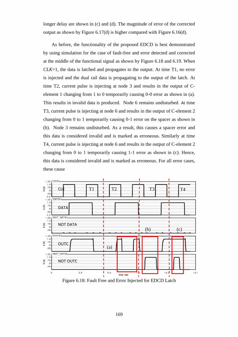
169
longer delay are shown in (c) and (d). The magnitude of error of the corrected
output as shown by Figure 6.17(d) is higher compared with Figure 6.16(d).
As before, the functionality of the proposed EDCD is best demonstrated
by using simulation for the case of fault-free and error detected and corrected
at the middle of the functional signal as shown by Figure 6.18 and 6.19. When
CLK=1, the data is latched and propagates to the output. At time T1, no error
is injected and the dual rail data is propagating to the output of the latch. At
time T2, current pulse is injecting at node 3 and results in the output of C-
element 1 changing from 1 to 0 temporarily causing 0-0 error as shown in (a).
This results in invalid data is produced. Node 6 remains undisturbed. At time
T3, current pulse is injecting at node 6 and results in the output of C-element 2
changing from 0 to 1 temporarily causing 0-1 error on the spacer as shown in
(b). Node 3 remains undisturbed. As a result, this causes a spacer error and
this data is considered invalid and is marked as erroneous. Similarly at time
T4, current pulse is injecting at node 6 and results in the output of C-element 2
changing from 0 to 1 temporarily causing 1-1 error as shown in (c). Hence,
this data is considered invalid and is marked as erroneous. For all error cases,
these cause
Figure 6.18: Fault Free and Error Injected for EDCD Latch
CLK
DATA
NOT DATA
OUTC
NOT OUTC
T1 T2 T3 T4
(a)
(b) (c)
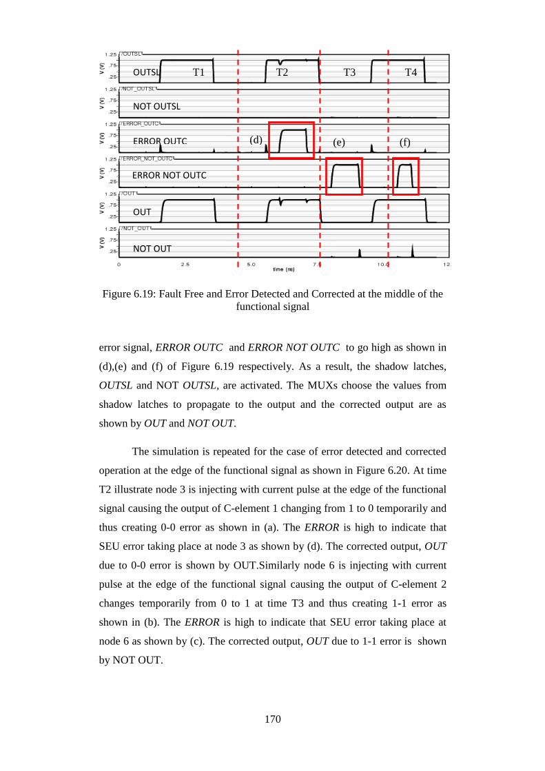
170
Figure 6.19: Fault Free and Error Detected and Corrected at the middle of the
functional signal
error signal, ERROR OUTC and ERROR NOT OUTC to go high as shown in
(d),(e) and (f) of Figure 6.19 respectively. As a result, the shadow latches,
OUTSL and NOT OUTSL, are activated. The MUXs choose the values from
shadow latches to propagate to the output and the corrected output are as
shown by OUT and NOT OUT.
The simulation is repeated for the case of error detected and corrected
operation at the edge of the functional signal as shown in Figure 6.20. At time
T2 illustrate node 3 is injecting with current pulse at the edge of the functional
signal causing the output of C-element 1 changing from 1 to 0 temporarily and
thus creating 0-0 error as shown in (a). The ERROR is high to indicate that
SEU error taking place at node 3 as shown by (d). The corrected output, OUT
due to 0-0 error is shown by OUT.Similarly node 6 is injecting with current
pulse at the edge of the functional signal causing the output of C-element 2
changes temporarily from 0 to 1 at time T3 and thus creating 1-1 error as
shown in (b). The ERROR is high to indicate that SEU error taking place at
node 6 as shown by (c). The corrected output, OUT due to 1-1 error is shown
by NOT OUT.
OUTSL
NOT OUTSL
ERROR OUTC
ERROR NOT OUTC
OUTC
OUT
NOT OUT
T1 T2 T3 T4
(d) (e) (f)
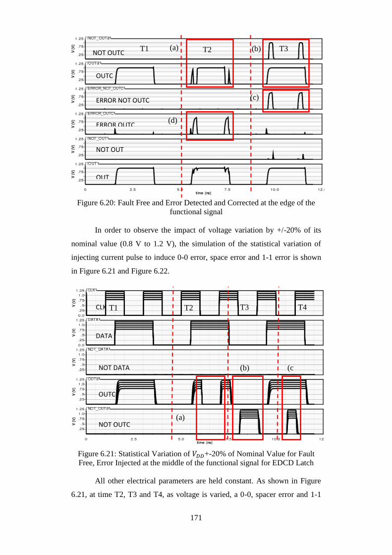
171
Figure 6.20: Fault Free and Error Detected and Corrected at the edge of the
functional signal
In order to observe the impact of voltage variation by +/-20% of its
nominal value (0.8 V to 1.2 V), the simulation of the statistical variation of
injecting current pulse to induce 0-0 error, space error and 1-1 error is shown
in Figure 6.21 and Figure 6.22.
Figure 6.21: Statistical Variation of 𝑉𝐷𝐷+-20% of Nominal Value for Fault
Free, Error Injected at the middle of the functional signal for EDCD Latch
All other electrical parameters are held constant. As shown in Figure
6.21, at time T2, T3 and T4, as voltage is varied, a 0-0, spacer error and 1-1
NOT OUTC
OUTC
ERROR NOT OUTC
ERROR OUTC
NOT OUT
OUT
T1 T2 T3 (a) (b)
(c)
(d)
T1 T2 T3 T4
(a)
(b) (c
)
CLK
DATA
NOT DATA
OUTC
NOT OUTC
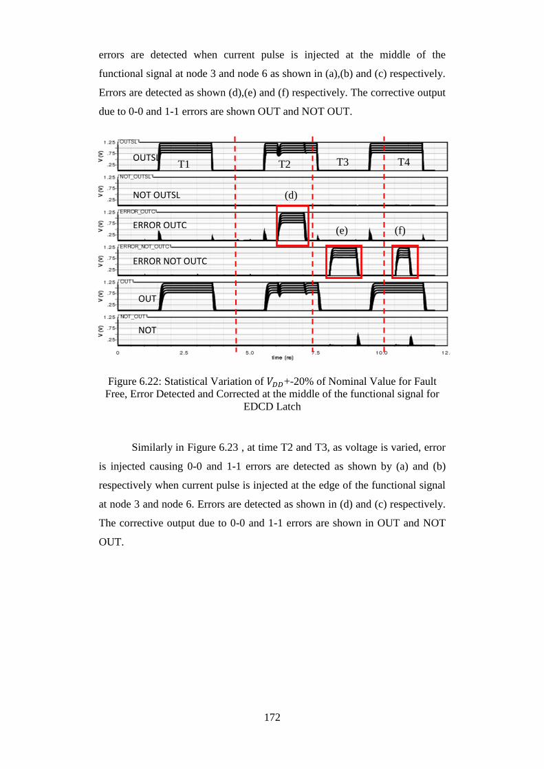
172
errors are detected when current pulse is injected at the middle of the
functional signal at node 3 and node 6 as shown in (a),(b) and (c) respectively.
Errors are detected as shown (d),(e) and (f) respectively. The corrective output
due to 0-0 and 1-1 errors are shown OUT and NOT OUT.
Figure 6.22: Statistical Variation of 𝑉𝐷𝐷+-20% of Nominal Value for Fault
Free, Error Detected and Corrected at the middle of the functional signal for
EDCD Latch
Similarly in Figure 6.23 , at time T2 and T3, as voltage is varied, error
is injected causing 0-0 and 1-1 errors are detected as shown by (a) and (b)
respectively when current pulse is injected at the edge of the functional signal
at node 3 and node 6. Errors are detected as shown in (d) and (c) respectively.
The corrective output due to 0-0 and 1-1 errors are shown in OUT and NOT
OUT.
T1 T2 T3 T4
(d)
(e) (f)
OUTSL
NOT OUTSL
ERROR OUTC
ERROR NOT OUTC
OUT
NOT
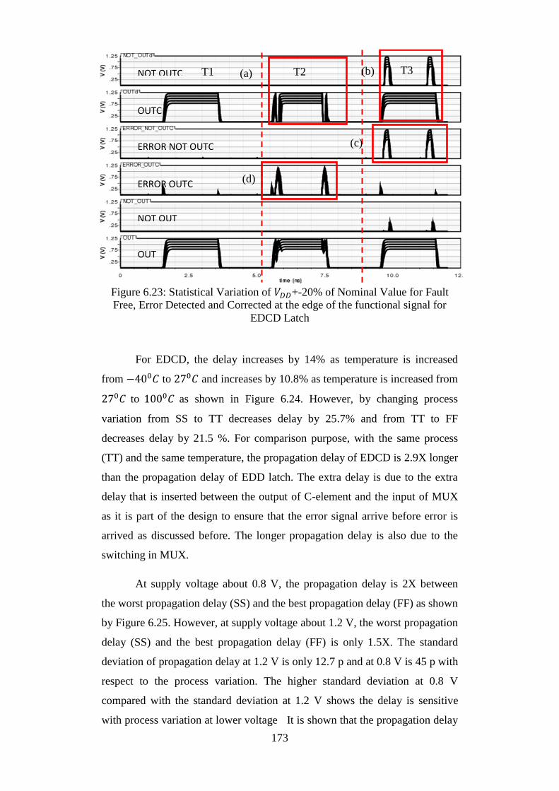
173
Figure 6.23: Statistical Variation of 𝑉𝐷𝐷+-20% of Nominal Value for Fault
Free, Error Detected and Corrected at the edge of the functional signal for
EDCD Latch
For EDCD, the delay increases by 14% as temperature is increased
from −400𝐶 to 270𝐶 and increases by 10.8% as temperature is increased from
270𝐶 to 1000𝐶 as shown in Figure 6.24. However, by changing process
variation from SS to TT decreases delay by 25.7% and from TT to FF
decreases delay by 21.5 %. For comparison purpose, with the same process
(TT) and the same temperature, the propagation delay of EDCD is 2.9X longer
than the propagation delay of EDD latch. The extra delay is due to the extra
delay that is inserted between the output of C-element and the input of MUX
as it is part of the design to ensure that the error signal arrive before error is
arrived as discussed before. The longer propagation delay is also due to the
switching in MUX.
At supply voltage about 0.8 V, the propagation delay is 2X between
the worst propagation delay (SS) and the best propagation delay (FF) as shown
by Figure 6.25. However, at supply voltage about 1.2 V, the worst propagation
delay (SS) and the best propagation delay (FF) is only 1.5X. The standard
deviation of propagation delay at 1.2 V is only 12.7 p and at 0.8 V is 45 p with
respect to the process variation. The higher standard deviation at 0.8 V
compared with the standard deviation at 1.2 V shows the delay is sensitive
with process variation at lower voltage It is shown that the propagation delay
NOT OUTC
OUTC
ERROR NOT OUTC
ERROR OUTC
NOT OUT
OUT
T1 T2 T3 (a) (b)
(c)
(d)
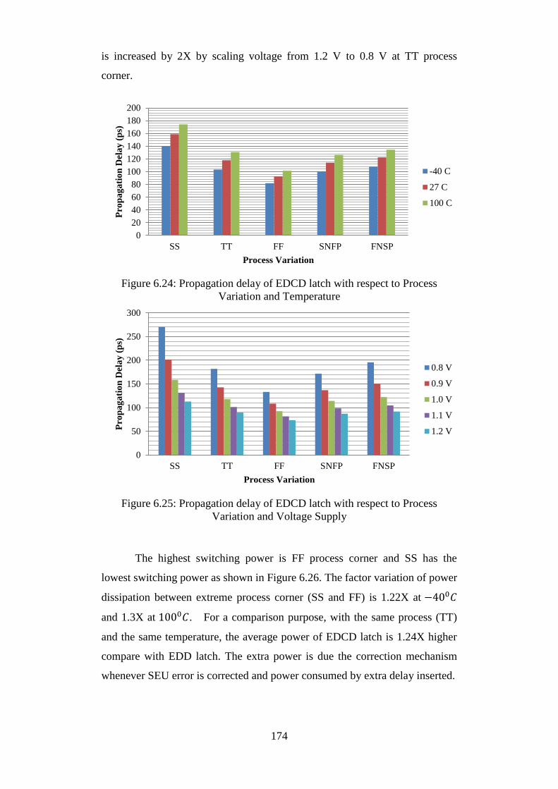
174
is increased by 2X by scaling voltage from 1.2 V to 0.8 V at TT process
corner.
Figure 6.24: Propagation delay of EDCD latch with respect to Process
Variation and Temperature
Figure 6.25: Propagation delay of EDCD latch with respect to Process
Variation and Voltage Supply
The highest switching power is FF process corner and SS has the
lowest switching power as shown in Figure 6.26. The factor variation of power
dissipation between extreme process corner (SS and FF) is 1.22X at −400𝐶
and 1.3X at 1000𝐶. For a comparison purpose, with the same process (TT)
and the same temperature, the average power of EDCD latch is 1.24X higher
compare with EDD latch. The extra power is due the correction mechanism
whenever SEU error is corrected and power consumed by extra delay inserted.
0
20
40
60
80
100
120
140
160
180
200
SS TT FF SNFP FNSP
Pro
pa
ga
tio
n D
ela
y (
ps)
Process Variation
-40 C
27 C
100 C
0
50
100
150
200
250
300
SS TT FF SNFP FNSP
Pro
pa
ga
tio
n D
ela
y (
ps)
Process Variation
0.8 V
0.9 V
1.0 V
1.1 V
1.2 V
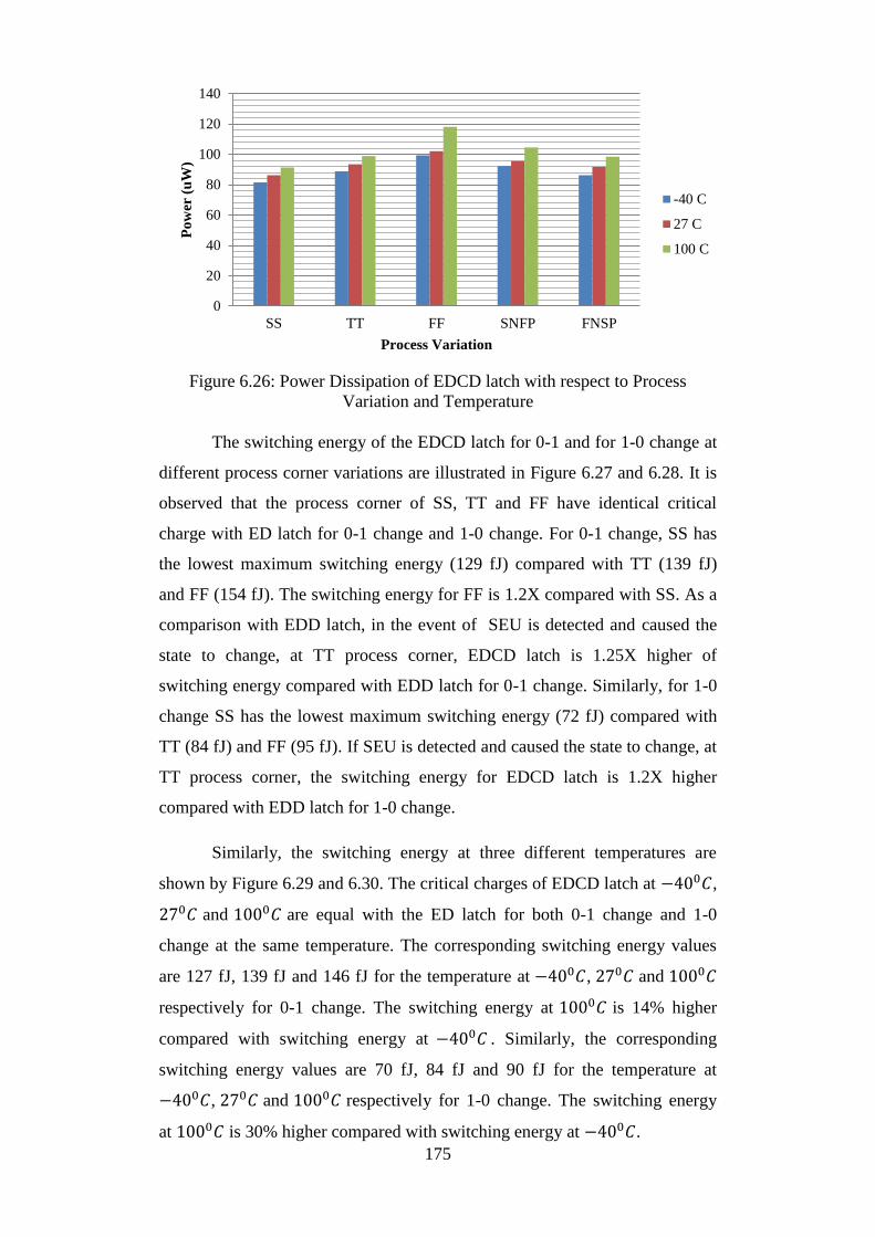
175
Figure 6.26: Power Dissipation of EDCD latch with respect to Process
Variation and Temperature
The switching energy of the EDCD latch for 0-1 and for 1-0 change at
different process corner variations are illustrated in Figure 6.27 and 6.28. It is
observed that the process corner of SS, TT and FF have identical critical
charge with ED latch for 0-1 change and 1-0 change. For 0-1 change, SS has
the lowest maximum switching energy (129 fJ) compared with TT (139 fJ)
and FF (154 fJ). The switching energy for FF is 1.2X compared with SS. As a
comparison with EDD latch, in the event of SEU is detected and caused the
state to change, at TT process corner, EDCD latch is 1.25X higher of
switching energy compared with EDD latch for 0-1 change. Similarly, for 1-0
change SS has the lowest maximum switching energy (72 fJ) compared with
TT (84 fJ) and FF (95 fJ). If SEU is detected and caused the state to change, at
TT process corner, the switching energy for EDCD latch is 1.2X higher
compared with EDD latch for 1-0 change.
Similarly, the switching energy at three different temperatures are
shown by Figure 6.29 and 6.30. The critical charges of EDCD latch at −400𝐶,
270𝐶 and 1000𝐶 are equal with the ED latch for both 0-1 change and 1-0
change at the same temperature. The corresponding switching energy values
are 127 fJ, 139 fJ and 146 fJ for the temperature at −400𝐶, 270𝐶 and 1000𝐶
respectively for 0-1 change. The switching energy at 1000𝐶 is 14% higher
compared with switching energy at −400𝐶 . Similarly, the corresponding
switching energy values are 70 fJ, 84 fJ and 90 fJ for the temperature at
−400𝐶, 270𝐶 and 1000𝐶 respectively for 1-0 change. The switching energy
at 1000𝐶 is 30% higher compared with switching energy at −400𝐶.
0
20
40
60
80
100
120
140
SS TT FF SNFP FNSP
Po
wer
(u
W)
Process Variation
-40 C
27 C
100 C
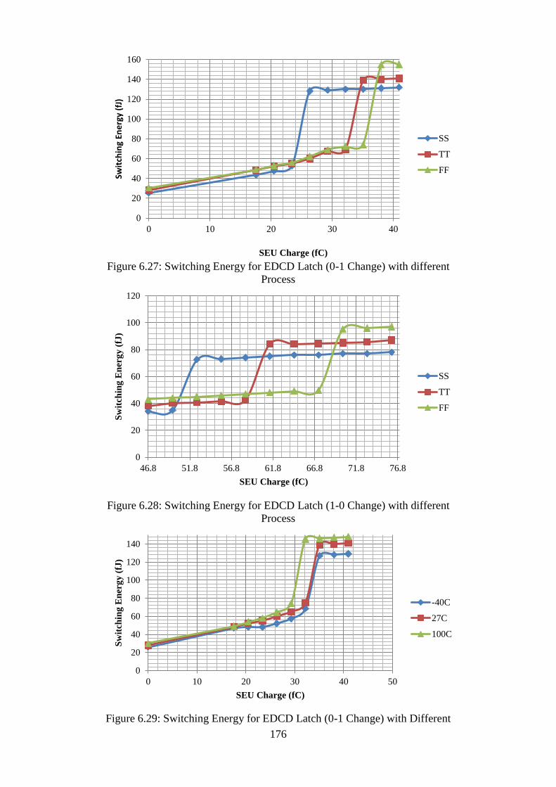
176
Figure 6.27: Switching Energy for EDCD Latch (0-1 Change) with different
Process
Figure 6.28: Switching Energy for EDCD Latch (1-0 Change) with different
Process
Figure 6.29: Switching Energy for EDCD Latch (0-1 Change) with Different
0
20
40
60
80
100
120
140
160
0 10 20 30 40
Swit
chin
g En
erg
y (f
J)
SEU Charge (fC)
SS
TT
FF
0
20
40
60
80
100
120
46.8 51.8 56.8 61.8 66.8 71.8 76.8
Sw
itch
ing
En
erg
y (
fJ)
SEU Charge (fC)
SS
TT
FF
0
20
40
60
80
100
120
140
0 10 20 30 40 50
Sw
itch
ing
En
erg
y (
fJ)
SEU Charge (fC)
-40C
27C
100C

177
Temperature
Figure 6.30: Switching Energy for EDCD Latch (1-0 Change) with Different
Temperature
The vulnerable nodes on EDCD latch are shown in Figure 6.31. Error
due to SEU on nodes 1,2,3,4,5 and 6 and nodes (a),(b),(e),(f),(g) and (h) are
detected and corrected. Only error due to SEU on nodes (c) and (d) are not
detected and corrected. Results are summarized in Table 6.2.
Component Vulnerable nodes Detected and corrected
error on the nodes
EDCD Latch 1,2,3,4,5 and 6 1,2,3,4,5 and 6
(a),(b),(c),(d),(e),(f),(g)
and (h)
(a),(b),(e),(f),(g) and (h)
Table 6.2: Vulnerable nodes on EDCD Latch
0
20
40
60
80
100
120
46.8 51.8 56.8 61.8 66.8 71.8
Sw
itch
ing
En
erg
y (
fJ)
SEU Charge (fC)
-40C
27C
100C
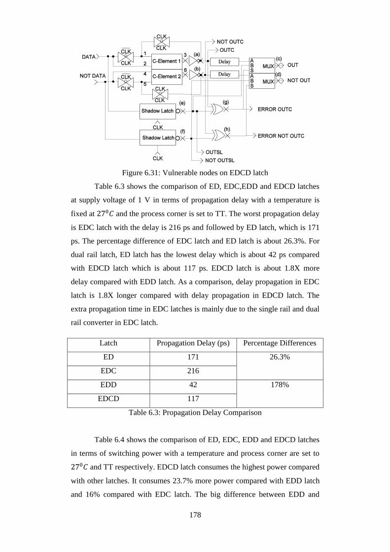
178
Figure 6.31: Vulnerable nodes on EDCD latch
Table 6.3 shows the comparison of ED, EDC,EDD and EDCD latches
at supply voltage of 1 V in terms of propagation delay with a temperature is
fixed at 270𝐶 and the process corner is set to TT. The worst propagation delay
is EDC latch with the delay is 216 ps and followed by ED latch, which is 171
ps. The percentage difference of EDC latch and ED latch is about 26.3%. For
dual rail latch, ED latch has the lowest delay which is about 42 ps compared
with EDCD latch which is about 117 ps. EDCD latch is about 1.8X more
delay compared with EDD latch. As a comparison, delay propagation in EDC
latch is 1.8X longer compared with delay propagation in EDCD latch. The
extra propagation time in EDC latches is mainly due to the single rail and dual
rail converter in EDC latch.
Latch Propagation Delay (ps) Percentage Differences
ED 171 26.3%
EDC 216
EDD 42 178%
EDCD 117
Table 6.3: Propagation Delay Comparison
Table 6.4 shows the comparison of ED, EDC, EDD and EDCD latches
in terms of switching power with a temperature and process corner are set to
270𝐶 and TT respectively. EDCD latch consumes the highest power compared
with other latches. It consumes 23.7% more power compared with EDD latch
and 16% compared with EDC latch. The big difference between EDD and
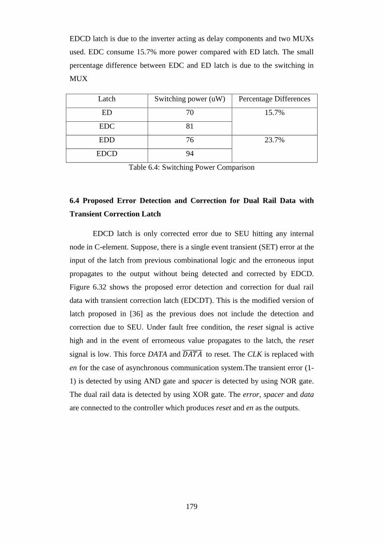
179
EDCD latch is due to the inverter acting as delay components and two MUXs
used. EDC consume 15.7% more power compared with ED latch. The small
percentage difference between EDC and ED latch is due to the switching in
MUX
Latch Switching power (uW) Percentage Differences
ED 70 15.7%
EDC 81
EDD 76 23.7%
EDCD 94
Table 6.4: Switching Power Comparison
6.4 Proposed Error Detection and Correction for Dual Rail Data with
Transient Correction Latch
EDCD latch is only corrected error due to SEU hitting any internal
node in C-element. Suppose, there is a single event transient (SET) error at the
input of the latch from previous combinational logic and the erroneous input
propagates to the output without being detected and corrected by EDCD.
Figure 6.32 shows the proposed error detection and correction for dual rail
data with transient correction latch (EDCDT). This is the modified version of
latch proposed in [36] as the previous does not include the detection and
correction due to SEU. Under fault free condition, the reset signal is active
high and in the event of errorneous value propagates to the latch, the reset
signal is low. This force DATA and 𝐷𝐴𝑇𝐴̅̅ ̅̅ ̅̅ ̅̅ to reset. The CLK is replaced with
en for the case of asynchronous communication system.The transient error (1-
1) is detected by using AND gate and spacer is detected by using NOR gate.
The dual rail data is detected by using XOR gate. The error, spacer and data
are connected to the controller which produces reset and en as the outputs.
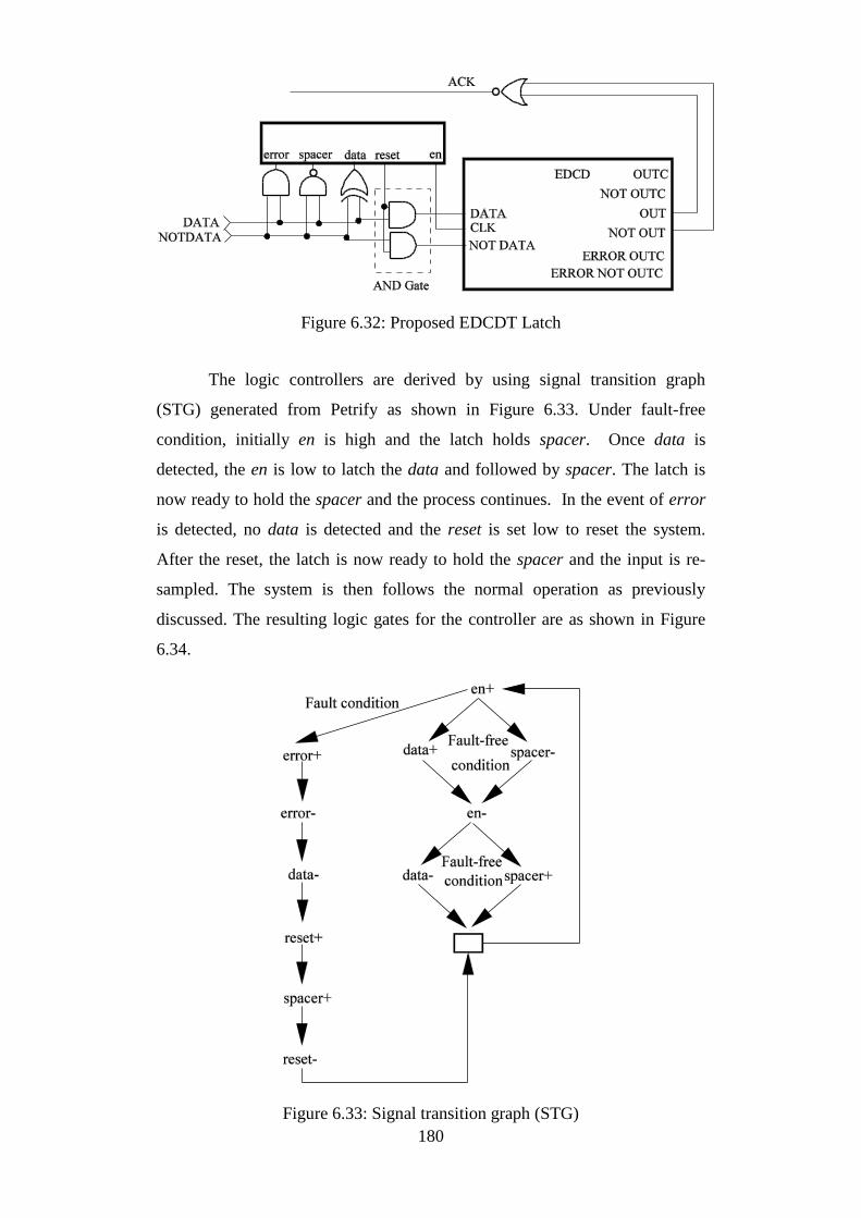
180
Figure 6.32: Proposed EDCDT Latch
The logic controllers are derived by using signal transition graph
(STG) generated from Petrify as shown in Figure 6.33. Under fault-free
condition, initially en is high and the latch holds spacer. Once data is
detected, the en is low to latch the data and followed by spacer. The latch is
now ready to hold the spacer and the process continues. In the event of error
is detected, no data is detected and the reset is set low to reset the system.
After the reset, the latch is now ready to hold the spacer and the input is re-
sampled. The system is then follows the normal operation as previously
discussed. The resulting logic gates for the controller are as shown in Figure
6.34.
Figure 6.33: Signal transition graph (STG)

181
Figure 6.34: Logic gates for the controller
The functionality of EDCDT is best described by using waveform.
Figure 6.35 shows the simulation of fault-free error, SEU error and transient
error. Figure 6.36 shows the simulation of control signal of the system. Under
fault-free condition as shown by time T1, dual rail data are detected and
propagate to the output. No SEU error and SET error are detected. The en goes
high to latch the data and the reset signal remains high. At time T2, a particle
hitting at node of EDCDT latch causing it to temporarily goes from 0-1, as
shown in Figure 6.35(a). This causes spacer error. At this instance, the output
of shadow latch propagates to the MUX to correct the corrupted output due to
SEU as shown by the output, NOT OUT. The error signal (ERROR NOT
OUTC) due to SEU (spacer error) is indicated by Figure 6.36(a). At time T3, a
particle hitting at node of EDCDT latch causing it to temporarily goes from 0-
1, as shown in Figure 6.35(b). This causes 1-1 error. Similarly, at this instance,
the output of shadow latch propagates to the MUX to correct the corrupted
output due to SEU as shown by the output, NOT OUT. The error signal
(ERROR NOT OUTC) due to SEU (1-1 error) is indicated in Figure 6.36(b).
At time T4, a transient error propagates to the latch. The error due to SET
(error) goes to 1 to indicate the presence of transient error as shown in Figure
6.35(c) and error is indicated in Figure 6.36(c). At this instances, no data and
spacer are detected as a result of SET error as shown in Figure 6.36(d) The
error detect the transient error causing the reset to go low as shown in Figure
6.36(e). Consequently, the erroneous data does not propagate to the output.
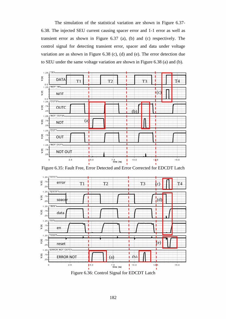
182
The simulation of the statistical variation are shown in Figure 6.37-
6.38. The injected SEU current causing spacer error and 1-1 error as well as
transient error as shown in Figure 6.37 (a), (b) and (c) respectively. The
control signal for detecting transient error, spacer and data under voltage
variation are as shown in Figure 6.38 (c), (d) and (e). The error detection due
to SEU under the same voltage variation are shown in Figure 6.38 (a) and (b).
Figure 6.35: Fault Free, Error Detected and Error Corrected for EDCDT Latch
Figure 6.36: Control Signal for EDCDT Latch
DATA
NOT
OUTC
NOT
OUT
NOT OUT
T1 T2 T3 T4
(c)
(b)
(a)
error
spacer
data
en
reset
ERROR NOT
OUTC NOU
(c)
(d)
(e)
(b) (a)
T1 T2 T3 T4
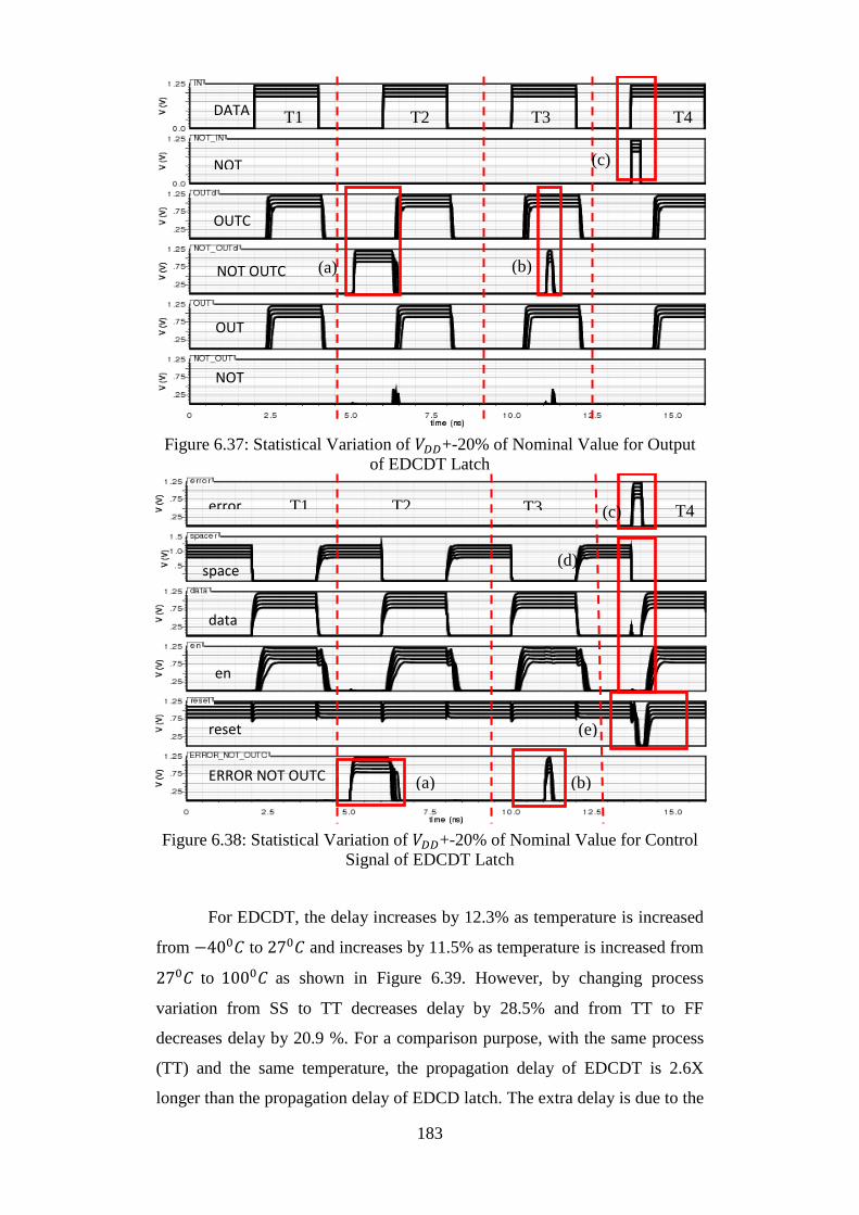
183
Figure 6.37: Statistical Variation of 𝑉𝐷𝐷+-20% of Nominal Value for Output
of EDCDT Latch
Figure 6.38: Statistical Variation of 𝑉𝐷𝐷+-20% of Nominal Value for Control
Signal of EDCDT Latch
For EDCDT, the delay increases by 12.3% as temperature is increased
from −400𝐶 to 270𝐶 and increases by 11.5% as temperature is increased from
270𝐶 to 1000𝐶 as shown in Figure 6.39. However, by changing process
variation from SS to TT decreases delay by 28.5% and from TT to FF
decreases delay by 20.9 %. For a comparison purpose, with the same process
(TT) and the same temperature, the propagation delay of EDCDT is 2.6X
longer than the propagation delay of EDCD latch. The extra delay is due to the
DATA
NOT
OUTC
NOT OUTC
OUT
NOT
T1 T2 T3 T4
(c)
(b) (a)
error
space
r
data
en
reset
ERROR NOT OUTC
T1 T2 T3 T4 (c)
(d)
(e)
(b) (a)

184
logic needed to detect transient error and produce reset and enable signal.
However, with the same conditions apply, the propagation delay of EDCDT is
only 1.4X longer than the propagation delay of EDC latch.
At supply voltage about 0.8 V, the propagation delay is 2.2X between
the worst propagation delay (SS) and the best propagation delay (FF) as shown
in Figure 6.40. However, at supply voltage about 1.2 V, the worst propagation
delay (SS) and the best propagation delay (FF) is only 1.6X. The standard
deviation of propagation delay at 1.2 V is only 61 p and at 0.8 V is 203 p with
respect to the process variation. It is shown that the propagation delay is
increased by 1.8X by scaling voltage from 1.2 V to 0.8 V at TT process
corner.
The factor variation of power dissipation between extreme process
corner (SS and FF) is 1.3X at −400𝐶 and 1.24X at 1000𝐶 as shown by Figure
6.41. For a comparison purpose, with the same process (TT) and the same
temperature (270𝐶 ), the average power of EDCDT latch is 2.7X higher
compare with EDCD latch. The extra power is due to the switching power by
the logic needed to detect transient error and produce reset and enable signal.
Figure 6.39: Propagation delay of EDCDT latch with respect to Process
Variation and Temperature
0
100
200
300
400
500
600
700
800
SS TT FF SNFP FNSP
Pro
pa
ga
tio
n D
ela
y (
ps)
Process Variation
-40 C
27 C
100 C

185
Figure 6.40: Propagation delay of EDCDT latch with respect to Process
Variation and Voltage Scaling
Figure 6.41: Power Dissipation of EDCDT latch with respect to Process
Variation and Temperature
Table 6.5 and Table 6.6 compares 10 latches in terms of area overhead
(by counting number of transistors) with respect to ED latch and error
correction capability. The proposed ED latch and EDC latch have higher area
overhead compared with previous proposed latches due to the logic gates
needed to convert the single-rail signals into dual-rail signals. However, for
EDD and EDCD latches, the overhead areas are comparable with the previous
proposed latches, especially FERST latch. The EDCDT latch and the proposed
latch [36] have almost the same overhead area, but EDCDT latch has the SEU
Error Detected and Corrected Capability in which the latch proposed by [36]
do not have the capability.
0
200
400
600
800
1000
1200
SS TT FF SNFP FNSP
Pro
pa
ga
tio
n D
ela
y (
ps)
Process Variation
0.8 V
0.9 V
1.0 V
1.1 V
1.2 V
0
100
200
300
400
500
600
700
800
SS TT FF SNFP FNSP
Po
wer
(u
W)
Process Variation
-40 C
27 C
100 C
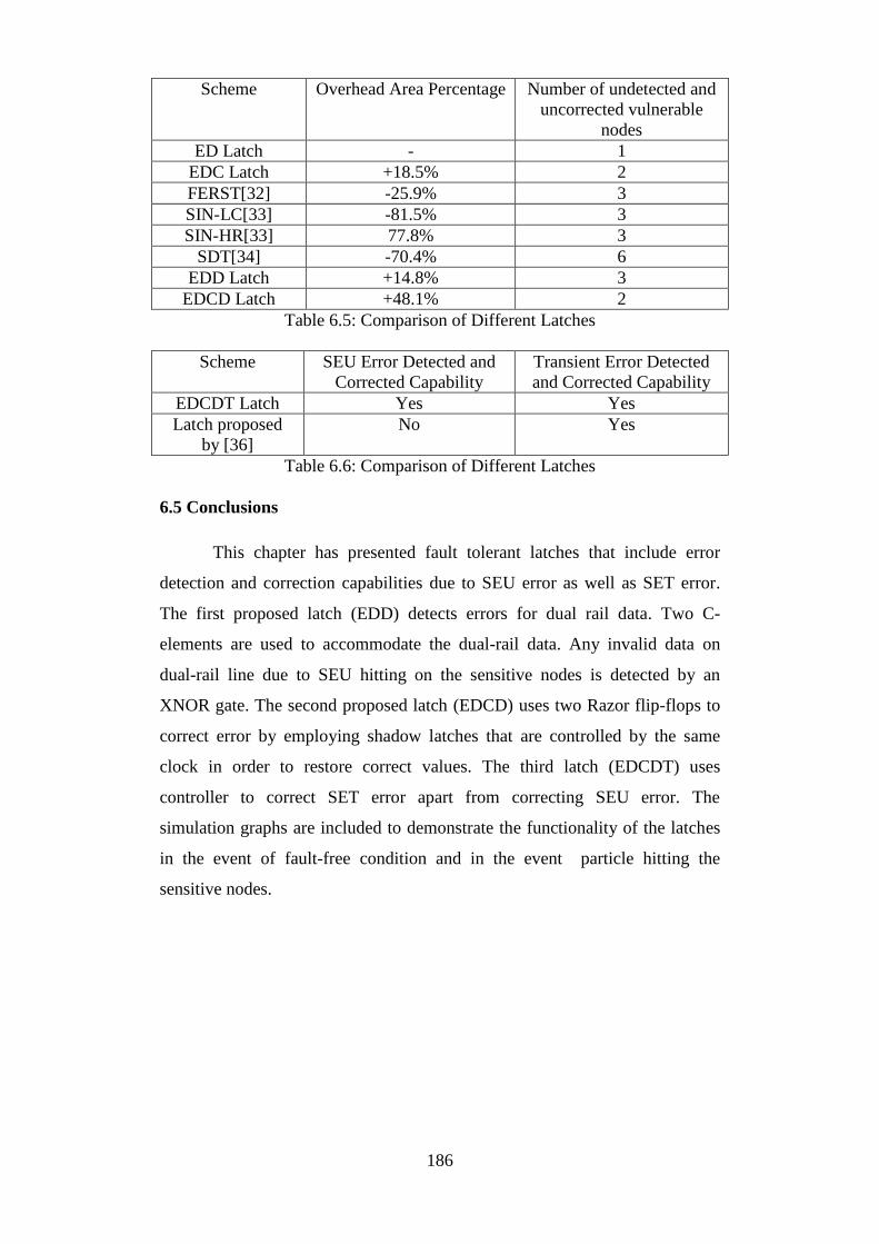
186
Scheme Overhead Area Percentage Number of undetected and
uncorrected vulnerable
nodes
ED Latch - 1
EDC Latch +18.5% 2
FERST[32] -25.9% 3
SIN-LC[33] -81.5% 3
SIN-HR[33] 77.8% 3
SDT[34] -70.4% 6
EDD Latch +14.8% 3
EDCD Latch +48.1% 2
Table 6.5: Comparison of Different Latches
Scheme SEU Error Detected and
Corrected Capability
Transient Error Detected
and Corrected Capability
EDCDT Latch Yes Yes
Latch proposed
by [36]
No Yes
Table 6.6: Comparison of Different Latches
6.5 Conclusions
This chapter has presented fault tolerant latches that include error
detection and correction capabilities due to SEU error as well as SET error.
The first proposed latch (EDD) detects errors for dual rail data. Two C-
elements are used to accommodate the dual-rail data. Any invalid data on
dual-rail line due to SEU hitting on the sensitive nodes is detected by an
XNOR gate. The second proposed latch (EDCD) uses two Razor flip-flops to
correct error by employing shadow latches that are controlled by the same
clock in order to restore correct values. The third latch (EDCDT) uses
controller to correct SET error apart from correcting SEU error. The
simulation graphs are included to demonstrate the functionality of the latches
in the event of fault-free condition and in the event particle hitting the
sensitive nodes.
187
Chapter 7. The design of Asynchronous Communication by
using the Proposed EDCD Latches
This chapter presents the systems that utilise the proposed EDCD latches.
Using Quartus II, the functionality EDCD latches are demonstrated by using
waveforms under fault free conditions and in the event of SEU hitting the
vulnerable nodes. An asynchronous communication is used to demonstrate the
functionality of EDCD latches. The effect of the system using latches that has
no capablity of detecting and correcting errors is also demonstrated in this
chapter.
7.1 Introduction
In this chapter, the functionality of error detection and correction for
dual rail (EDCD) latches are verified by using Quartus II from Altera. The
functionality of error detection and correction for single rail (EDC) on
complex logic is shown in Appendix B. Previously, Cadence UMC 90nm
technology is used to construct the latches at transistor-level design. In order
to design the proposed latches in Quartus II, some modifications have to be
made on the design. While there is a standard gates and logic available in
library of Quartus II, some non-standard logic are not available such as C-
element. VHDL is used to describe the behaviour of non-standard logic as
shown by Algorithm 7.1 and 7.2. Previously, the C-element and shadow latch
are constructed at transistors level by using UMC90 nm technology. The result
of synthesize C-element and shadow latch are shown in Figure 7.1 and Figure
7.2 respectively.
7.2 Asynchronous communication by using EDCD Latch
The injection method by using XOR gate is used to simulate the state
change in EDCD latch. Two XOR gates are inserted at the output of C-
element 1 and C-element 2 as shown by the dashed-box in Figure 7.3. The first
port of XOR gate is fed with the output of C-element and the second port of
XOR gate is fed with errors as denoted by e1 and e2.
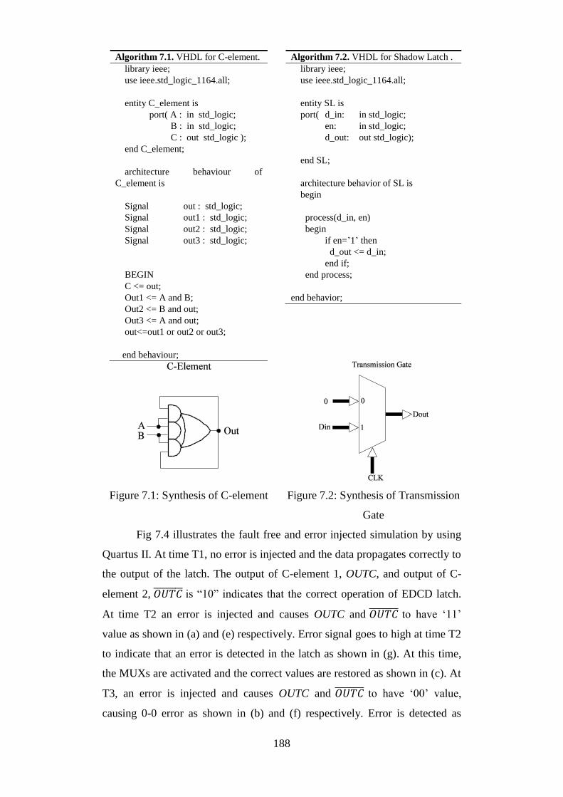
188
Algorithm 7.1. VHDL for C-element.
library ieee;
use ieee.std_logic_1164.all;
entity C_element is
port( A : in std_logic;
B : in std_logic;
C : out std_logic );
end C_element;
architecture behaviour of
C_element is
Signal out : std_logic;
Signal out1 : std_logic;
Signal out2 : std_logic;
Signal out3 : std_logic;
BEGIN
C <= out;
Out1 <= A and B;
Out2 <= B and out;
Out3 <= A and out;
out<=out1 or out2 or out3;
end behaviour;
Algorithm 7.2. VHDL for Shadow Latch .
library ieee;
use ieee.std_logic_1164.all;
entity SL is
port( d_in: in std_logic;
en: in std_logic;
d_out: out std_logic);
end SL;
architecture behavior of SL is
begin
process(d_in, en)
begin
if en=’1’ then
d_out <= d_in;
end if;
end process;
end behavior;
Figure 7.1: Synthesis of C-element Figure 7.2: Synthesis of Transmission
Gate
Fig 7.4 illustrates the fault free and error injected simulation by using
Quartus II. At time T1, no error is injected and the data propagates correctly to
the output of the latch. The output of C-element 1, OUTC, and output of C-
element 2, 𝑂𝑈𝑇𝐶̅̅ ̅̅ ̅̅ ̅̅ is “10” indicates that the correct operation of EDCD latch.
At time T2 an error is injected and causes OUTC and 𝑂𝑈𝑇𝐶̅̅ ̅̅ ̅̅ ̅̅ to have ‘11’
value as shown in (a) and (e) respectively. Error signal goes to high at time T2
to indicate that an error is detected in the latch as shown in (g). At this time,
the MUXs are activated and the correct values are restored as shown in (c). At
T3, an error is injected and causes OUTC and 𝑂𝑈𝑇𝐶̅̅ ̅̅ ̅̅ ̅̅ to have ‘00’ value,
causing 0-0 error as shown in (b) and (f) respectively. Error is detected as
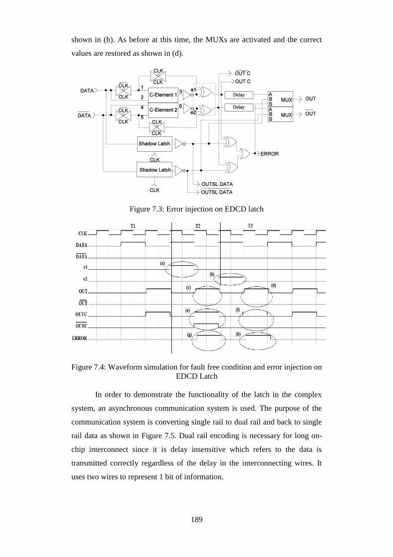
189
shown in (h). As before at this time, the MUXs are activated and the correct
values are restored as shown in (d).
Figure 7.3: Error injection on EDCD latch
Figure 7.4: Waveform simulation for fault free condition and error injection on
EDCD Latch
In order to demonstrate the functionality of the latch in the complex
system, an asynchronous communication system is used. The purpose of the
communication system is converting single rail to dual rail and back to single
rail data as shown in Figure 7.5. Dual rail encoding is necessary for long on-
chip interconnect since it is delay insensitive which refers to the data is
transmitted correctly regardless of the delay in the interconnecting wires. It
uses two wires to represent 1 bit of information.
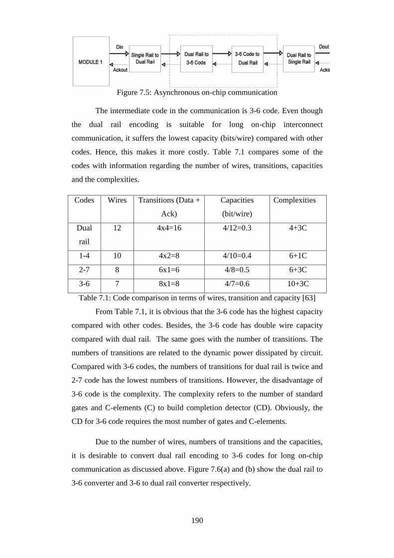
190
Figure 7.5: Asynchronous on-chip communication
The intermediate code in the communication is 3-6 code. Even though
the dual rail encoding is suitable for long on-chip interconnect
communication, it suffers the lowest capacity (bits/wire) compared with other
codes. Hence, this makes it more costly. Table 7.1 compares some of the
codes with information regarding the number of wires, transitions, capacities
and the complexities.
Codes Wires Transitions (Data +
Ack)
Capacities
(bit/wire)
Complexities
Dual
rail
12 4x4=16 4/12=0.3 4+3C
1-4 10 4x2=8 4/10=0.4 6+1C
2-7 8 6x1=6 4/8=0.5 6+3C
3-6 7 8x1=8 4/7=0.6 10+3C
Table 7.1: Code comparison in terms of wires, transition and capacity [63]
From Table 7.1, it is obvious that the 3-6 code has the highest capacity
compared with other codes. Besides, the 3-6 code has double wire capacity
compared with dual rail. The same goes with the number of transitions. The
numbers of transitions are related to the dynamic power dissipated by circuit.
Compared with 3-6 codes, the numbers of transitions for dual rail is twice and
2-7 code has the lowest numbers of transitions. However, the disadvantage of
3-6 code is the complexity. The complexity refers to the number of standard
gates and C-elements (C) to build completion detector (CD). Obviously, the
CD for 3-6 code requires the most number of gates and C-elements.
Due to the number of wires, numbers of transitions and the capacities,
it is desirable to convert dual rail encoding to 3-6 codes for long on-chip
communication as discussed above. Figure 7.6(a) and (b) show the dual rail to
3-6 converter and 3-6 to dual rail converter respectively.

191
(a) : Dual rail to 3-6 converter (b) : 3-6 to dual rail converter
Figure 7.6
The conversion of the dual rail to 3-6 code back to dual rail code is
shown in Figure 7.7. Each of the pipelines is enabled from subsequent
pipeline stage. The enable signal is obtained from the (CD) of the subsequent
pipeline stage before it is inverted into second port of C-element of the
previous pipeline. The on-chip communication consists of three pipelines.
The first register pipeline buffers the input of dual rail data and the CD detects
the presence of dual rail data at the output of the first pipelines. This provides
acknowledge signal to the preceding pipeline. The second pipeline outputs the
3-6 code from dual rail to 3-6 converter and the CD detects the presence of 3-6
acknowledge signal. The acknowledge signal is used to enable and disable the
first pipeline. The third pipeline outputs the dual rail data from 3-6 to dual rail
converter and allowing the acknowledge signal from CD that detects the
presence of dual rail data. The CD signal is used to enable and disable the
second pipeline. It is desired to build the latch from pipeline by using EDCD
latch and the effect of using EDCD latch in the event of current pulse hit to
one of latches in the pipeline is discussed below.
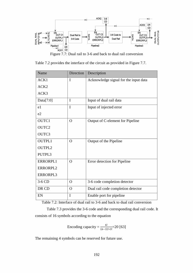
192
Figure 7.7: Dual rail to 3-6 and back to dual rail conversion
Table 7.2 provides the interface of the circuit as provided in Figure 7.7.
Name Direction Description
ACK1
ACK2
ACK3
I Acknowledge signal for the input data
Data[7:0] I Input of dual rail data
e1
e2
I Input of injected error
OUTC1
OUTC2
OUTC3
O Output of C-element for Pipeline
OUTPL1
OUTPL2
PUTPL3
O Output of the Pipeline
ERRORPL1
ERRORPL2
ERRORPL3
O Error detection for Pipeline
3-6 CD O 3-6 code completion detector
DR CD O Dual rail code completion detector
EN I Enable port for pipeline
Table 7.2: Interface of dual rail to 3-6 and back to dual rail conversion
Table 7.3 provides the 3-6 code and the corresponding dual rail code. It
consists of 16 symbols according to the equation
Encoding capacity = 6!
(6−3)!∗3!=20 [63]
The remaining 4 symbols can be reserved for future use.
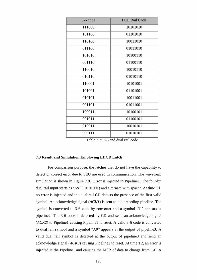
193
3-6 code Dual Rail Code
111000 10101010
101100 01101010
110100 10011010
011100 01011010
101010 10100110
001110 01100110
110010 10010110
010110 01010110
110001 10101001
101001 01101001
010101 10011001
001101 01011001
100011 10100101
001011 01100101
010011 10010101
000111 01010101
Table 7.3: 3-6 and dual rail code
7.3 Result and Simulation Employing EDCD Latch
For comparison purpose, the latches that do not have the capability to
detect or correct error due to SEU are used in communication. The waveform
simulation is shown in Figure 7.8. Error is injected to Pipeline1. The four-bit
dual rail input starts as ‘A9’ (10101001) and alternate with spacer. At time T1,
no error is injected and the dual rail CD detects the presence of the first valid
symbol. An acknowledge signal (ACK1) is sent to the preceding pipeline. The
symbol is converted to 3-6 code by converter and a symbol ‘31’ appears at
pipeline2. The 3-6 code is detected by CD and send an acknowledge signal
(ACK2) to Pipeline1 causing Pipeline1 to reset. A valid 3-6 code is converted
to dual rail symbol and a symbol “A9” appears at the output of pipeline3. A
valid dual rail symbol is detected at the output of pipeline3 and send an
acknowledge signal (ACK3) causing Pipeline2 to reset. At time T2, an error is
injected at the Pipeline1 and causing the MSB of data to change from 1-0. A
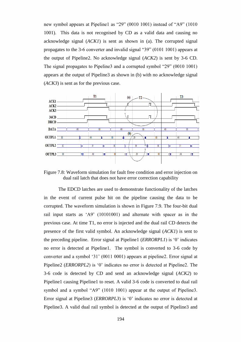
194
new symbol appears at Pipeline1 as “29” (0010 1001) instead of “A9” (1010
1001). This data is not recognised by CD as a valid data and causing no
acknowledge signal (ACK1) is sent as shown in (a). The corrupted signal
propagates to the 3-6 converter and invalid signal “39” (0101 1001) appears at
the output of Pipeline2. No acknowledge signal (ACK2) is sent by 3-6 CD.
The signal propagates to Pipeline3 and a corrupted symbol “29” (0010 1001)
appears at the output of Pipeline3 as shown in (b) with no acknowledge signal
(ACK3) is sent as for the previous case.
Figure 7.8: Waveform simulation for fault free condition and error injection on
dual rail latch that does not have error correction capability
The EDCD latches are used to demonstrate functionality of the latches
in the event of current pulse hit on the pipeline causing the data to be
corrupted. The waveform simulation is shown in Figure 7.9. The four-bit dual
rail input starts as ‘A9’ (10101001) and alternate with spacer as in the
previous case. At time T1, no error is injected and the dual rail CD detects the
presence of the first valid symbol. An acknowledge signal (ACK1) is sent to
the preceding pipeline. Error signal at Pipeline1 (ERRORPL1) is ‘0’ indicates
no error is detected at Pipeline1. The symbol is converted to 3-6 code by
converter and a symbol ‘31’ (0011 0001) appears at pipeline2. Error signal at
Pipeline2 (ERRORPL2) is ‘0’ indicates no error is detected at Pipeline2. The
3-6 code is detected by CD and send an acknowledge signal (ACK2) to
Pipeline1 causing Pipeline1 to reset. A valid 3-6 code is converted to dual rail
symbol and a symbol “A9” (1010 1001) appear at the output of Pipeline3.
Error signal at Pipeline3 (ERRORPL3) is ‘0’ indicates no error is detected at
Pipeline3. A valid dual rail symbol is detected at the output of Pipeline3 and
195
send an acknowledge (ACK3) signal causing Pipeline2 to reset. At time T2, an
error is injected as shown in (a) at the Pipeline1 and causing the second MSB
of data to change from 0-1. A new symbol appears at output of C-element
(OUTC1) as “E9” (1110 1001) instead of “A9” (1010 1001) as shown in (e).
This is an example of 1-1 error. At this instance, error signal at Pipeline1 is
produced (ERRORPL1) to indicate that error is detected on Pipeline1 as shown
in (c). As a result of error is detected, the MUXs are activated to replace the
corrupted values with the true value. The true value of “A9” (1010 1001)
appears at OUTPL1 as shown in (g). With the correction mechanism in place,
the dual rail CD is able to detect the presence of valid dual rail and
acknowledge signal (ACK1) is sent to the preceding pipeline. The corrected
dual rail values are converted to 3-6 code and a symbol of “31” (0011 0001)
appears the output of pipeline2 as shown in (g). The 3-6 CD recognise it as a
valid data and sent an acknowledge signal (ACK2) to Pipeline1 and causing it
to reset. No error signal is produced (ERRORPL2) at Pipeline2 to indicate that
no error is detected on Pipeline2. The data is converted back to dual rail and a
symbol of “A9” (1010 1001) appears at the output of Pipeline3 as shown in
(g). Similarly no error is produced (ERRORPL3) at Pipeline3 to indicate that
no error is detected on Pipeline3.
At time T3 an error is injected as shown in (b) at the Pipeline1 and
causing the MSB of data to change from 1-0. A new symbol appears at output
of C-element (OUTC1) as “29” (0010 1001) instead of “A9” (1010 1001) as
shown in (f). This is an example of 0-0 error. At this instance, error signal at
pipeline1 is produced (ERRORPL1) to indicate that error is detected on
Pipeline1 as shown in (d). As a result of error is detected, the MUXs are
activated to replace the corrupted values with the true value. The data proceed
to converters, and Pipeline2 and Ppipeline3 with the same protocols as
described above as shown in (h).
With the 0-0 and 1-1 errors occur at pipeline, the proposed EDCD
latches are able to detect and correct error as shown by the waveform in Figure
7.9.

196
Figure 7.9: Waveform simulation for fault free condition and error injection on
EDCD latch
7.4 Conclusions
This chapter has presented the application of EDCD latch. The EDC
latch is used as a pipeline in the adder system and the EDCD latch is used as a
pipeline in the asynchronous communication. For this purpose, Quartus II
software is used to obtain the waveform of the simulation. To emulate the
SEU hitting on the sensitive node, the XOR is placed at the output of the latch.
One port is connected to the output of C-element and the other port is used to
the error. Two simulations are performed to demonstrate the functionality of
EDCD latch. The first simulation is the data transfer by using latches that do
not have the capability of detecting and correcting errors. The second
simulation is by using EDCD latches. It is proven that simulation by using
EDCD latches are able to counter SEU error for the case of dual rail
asynchronous communication.
197
Chapter 8. Conclusions and Further Work
Chapter 8 presents conclusions and future work related to the project.
8.1 Conclusions
Single event upset (SEU) can cause system failures or produce
incorrect values in a digital system. Such problems become extremely severe
in emerging submicron technologies due to the transistors and voltage supply
scaling. This scaling causes physical features of transistors, drain current and
threshold voltage to reduce, making them more vulnerable to SEU. The
increasing demand for low power consumption and system complexities has
necessitated the analysis of SEU and mitigation of the effect of SEU in digital
systems. Apart from voltage and size scaling of transistors, other factors that
can affect the vulnerability of the circuits towards SEU include process
variation and temperature. Process variation refers to inaccuracies in the
manufacturing process and can lead to deterioration of circuit performance and
an increase in power consumption. As for temperature, it degrades the
threshold voltage, carrier mobility and saturation velocity of transistors. As a
result of degrading carrier mobility, the drain current becomes lower and the
sensitivity of the node towards SEU is increased.
The first step in this research was to analyse the occurrence of soft
error on four different configurations of C-elements: SIL, SC, SS and DIL.
The sensitive nodes on different C-elements were identified and injected with
current pulse. The current pulse causing SEU was modelled with fast rising
time and slow falling time. The amplitude of current was varied until the state
was changed at the output of the C-elements. The charge corresponding to the
state change is known as the critical charge. The experiments were repeated
with respect to the change of the process corner, temperature, voltage and size
scaling. The standard deviations of all nodes in all C-elements were compared.
The SIL configuration had the highest standard deviation for all changes,
which implies that SIL is the most sensitive C-element compared with other
configurations.
198
Next, a new method was developed to calculate the error rate of the
four C-element circuits with respect to process corner, temperature, voltage
and size scaling. The method took into consideration the probability of being
hit by current pulse. The error rates and the standard deviation of error rates
were calculated and compared between C-elements. Results show that SS and
DIL have the highest error rates and highest standard deviations compared
with SIL and SC. It is concluded, therefore, that SIL and SC are the most
stable C-elements compared with the SS and DIL configurations.
The focus of the third stage was to mitigate the effect of SEU by
designing error detection and correction latches in response to SEU. Two
types of latches were proposed, EDC and EDCD latches for single and dual
rail respectively. By using Cadence UMC 90nm, the functionality of both
types of latches can be demonstrated by using waveforms under fault free
conditions and in the event of a current pulse striking the vulnerable nodes.
The performances of both latches were studied in terms of propagation delay
versus process corner, temperature and voltage supply. The switching energy
of both latches can be obtained in the event of the current charge being less
than, equal to or more than the critical charge with different process corners
and temperatures. The error detection and correction as well as transient error
correction latch (EDCDT) were also proposed to correct transient error in
addition to correcting SEU error.
The focus of the fourth stage was to design asynchronous
communication. The main purpose of designing the system was to test the
functionality of the EDCD latch by injecting an error into one of the latches.
This was demonstrated by using waveforms under fault free conditions and in
the event of SEU hitting the vulnerable nodes. Quartus II software was used to
design the systems. The effect of the system using latches in terms of it having
no capablity of detecting and correcting errors was also demonstrated in order
to compare the correction capability of the latch
8.2 Further Work
This section discusses possible extensions to this research. Future work could
include the following:

199
(a) Designing an error correction latch due to charge sharing. As transistors
continue to shrink, distances between the hit devices and the adjacent
devices have become very close and this results in the diffusion of the
charge to the adjacent node. The proposed error correction latches
(EDC and EDCD latches) have addressed SEU for charge collecting at
single nodes. The work can be extended to include error collection due
to the charge sharing (charge collection at several nodes induced by a
single event transient (SET)).
(b) Silicon implementation can be used to measure error rate of the EDC
and EDCD latches instead of using a Field Programmable Gates Array
(FPGA). This is due to the delay in each of the blocks in FPGA. It is
expected that the error rate measurements in silicon implementation
would be less than in FPGA due to the propagation delay in FPGA,
especially at lower voltages, where timing error is more significant than
injected error.
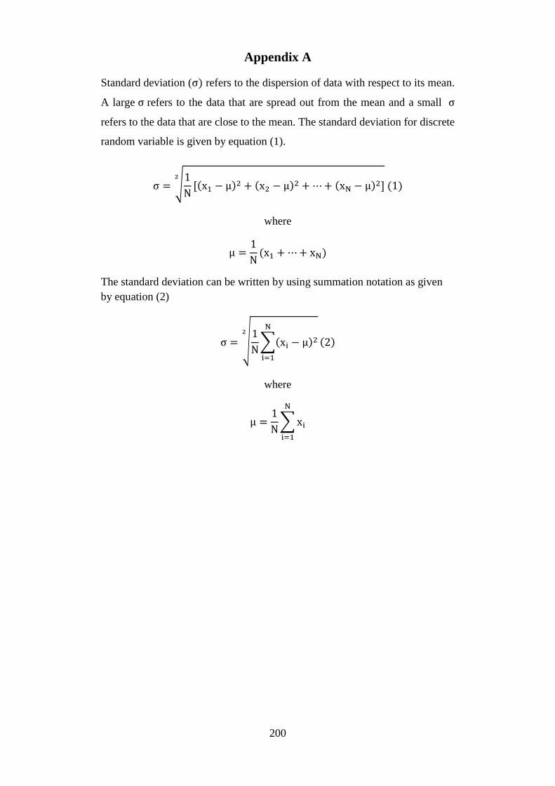
200
Appendix A
Standard deviation (σ) refers to the dispersion of data with respect to its mean.
A large σ refers to the data that are spread out from the mean and a small σ
refers to the data that are close to the mean. The standard deviation for discrete
random variable is given by equation (1).
σ = √1
N[(x1 − μ)2 + (x2 − μ)2 +⋯+ (xN − μ)2]
2
(1)
where
μ =1
N(x1 +⋯+ xN)
The standard deviation can be written by using summation notation as given
by equation (2)
σ = √1
N∑(xi − μ)2N
i=1
2
(2)
where
μ =1
N∑xi
N
i=1
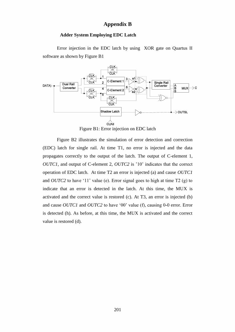
201
Appendix B
Adder System Employing EDC Latch
Error injection in the EDC latch by using XOR gate on Quartus II
software as shown by Figure B1
Figure B1: Error injection on EDC latch
Figure B2 illustrates the simulation of error detection and correction
(EDC) latch for single rail. At time T1, no error is injected and the data
propagates correctly to the output of the latch. The output of C-element 1,
OUTC1, and output of C-element 2, OUTC2 is ’10’ indicates that the correct
operation of EDC latch. At time T2 an error is injected (a) and cause OUTC1
and OUTC2 to have ‘11’ value (e). Error signal goes to high at time T2 (g) to
indicate that an error is detected in the latch. At this time, the MUX is
activated and the correct value is restored (c). At T3, an error is injected (b)
and cause OUTC1 and OUTC2 to have ‘00’ value (f), causing 0-0 error. Error
is detected (h). As before, at this time, the MUX is activated and the correct
value is restored (d).
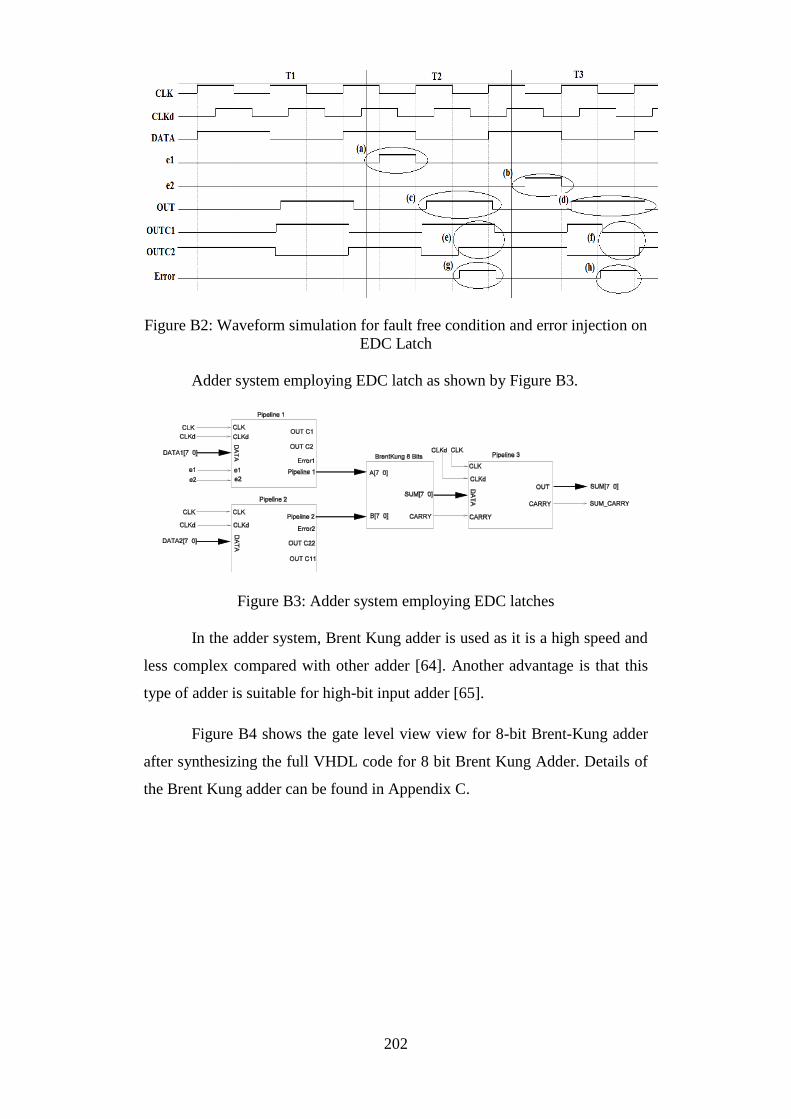
202
Figure B2: Waveform simulation for fault free condition and error injection on
EDC Latch
Adder system employing EDC latch as shown by Figure B3.
Figure B3: Adder system employing EDC latches
In the adder system, Brent Kung adder is used as it is a high speed and
less complex compared with other adder [64]. Another advantage is that this
type of adder is suitable for high-bit input adder [65].
Figure B4 shows the gate level view view for 8-bit Brent-Kung adder
after synthesizing the full VHDL code for 8 bit Brent Kung Adder. Details of
the Brent Kung adder can be found in Appendix C.
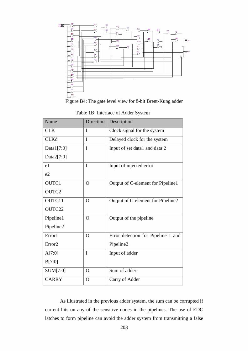
203
Figure B4: The gate level view for 8-bit Brent-Kung adder
Table 1B: Interface of Adder System
Name Direction Description
CLK I Clock signal for the system
CLKd I Delayed clock for the system
Data1[7:0]
Data2[7:0]
I Input of set data1 and data 2
e1
e2
I Input of injected error
OUTC1
OUTC2
O Output of C-element for Pipeline1
OUTC11
OUTC22
O Output of C-element for Pipeline2
Pipeline1
Pipeline2
O Output of the pipeline
Error1
Error2
O Error detection for Pipeline 1 and
Pipeline2
A[7:0]
B[7:0]
I Input of adder
SUM[7:0] O Sum of adder
CARRY O Carry of Adder
As illustrated in the previous adder system, the sum can be corrupted if
current hits on any of the sensitive nodes in the pipelines. The use of EDC
latches to form pipeline can avoid the adder system from transmitting a false
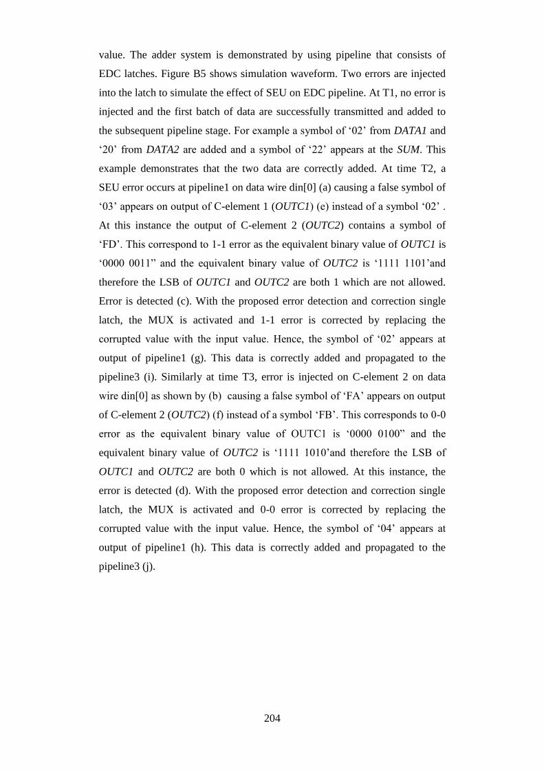
204
value. The adder system is demonstrated by using pipeline that consists of
EDC latches. Figure B5 shows simulation waveform. Two errors are injected
into the latch to simulate the effect of SEU on EDC pipeline. At T1, no error is
injected and the first batch of data are successfully transmitted and added to
the subsequent pipeline stage. For example a symbol of ‘02’ from DATA1 and
‘20’ from DATA2 are added and a symbol of ‘22’ appears at the SUM. This
example demonstrates that the two data are correctly added. At time T2, a
SEU error occurs at pipeline1 on data wire din[0] (a) causing a false symbol of
‘03’ appears on output of C-element 1 (OUTC1) (e) instead of a symbol ‘02’ .
At this instance the output of C-element 2 (OUTC2) contains a symbol of
‘FD’. This correspond to 1-1 error as the equivalent binary value of OUTC1 is
‘0000 0011” and the equivalent binary value of OUTC2 is ‘1111 1101’and
therefore the LSB of OUTC1 and OUTC2 are both 1 which are not allowed.
Error is detected (c). With the proposed error detection and correction single
latch, the MUX is activated and 1-1 error is corrected by replacing the
corrupted value with the input value. Hence, the symbol of ‘02’ appears at
output of pipeline1 (g). This data is correctly added and propagated to the
pipeline3 (i). Similarly at time T3, error is injected on C-element 2 on data
wire din[0] as shown by (b) causing a false symbol of ‘FA’ appears on output
of C-element 2 (OUTC2) (f) instead of a symbol ‘FB’. This corresponds to 0-0
error as the equivalent binary value of OUTC1 is ‘0000 0100” and the
equivalent binary value of OUTC2 is ‘1111 1010’and therefore the LSB of
OUTC1 and OUTC2 are both 0 which is not allowed. At this instance, the
error is detected (d). With the proposed error detection and correction single
latch, the MUX is activated and 0-0 error is corrected by replacing the
corrupted value with the input value. Hence, the symbol of ‘04’ appears at
output of pipeline1 (h). This data is correctly added and propagated to the
pipeline3 (j).
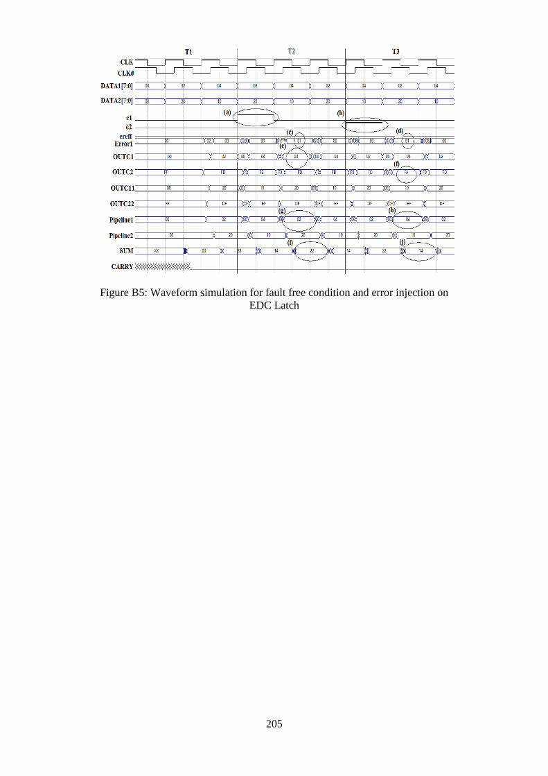
205
Figure B5: Waveform simulation for fault free condition and error injection on
EDC Latch
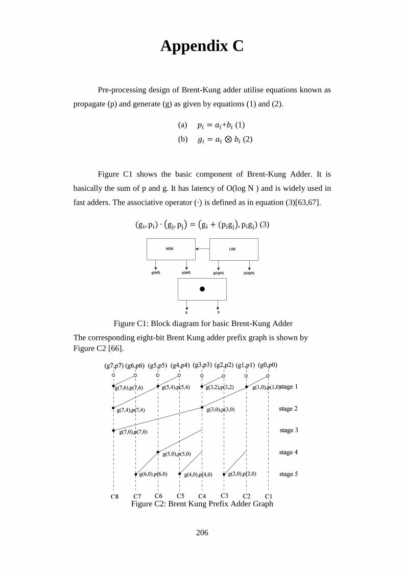
206
Appendix C
Pre-processing design of Brent-Kung adder utilise equations known as
propagate (p) and generate (g) as given by equations (1) and (2).
(a) 𝑝𝑖 = 𝑎𝑖+𝑏𝑖 (1)
(b) 𝑔𝑖 = 𝑎𝑖⊗𝑏𝑖 (2)
Figure C1 shows the basic component of Brent-Kung Adder. It is
basically the sum of p and g. It has latency of O(log N ) and is widely used in
fast adders. The associative operator (∙) is defined as in equation (3)[63,67].
(gi, pi) ∙ (gj, pj) = (gi + (pigj), pigj) (3)
Figure C1: Block diagram for basic Brent-Kung Adder
The corresponding eight-bit Brent Kung adder prefix graph is shown by
Figure C2 [66].
Figure C2: Brent Kung Prefix Adder Graph
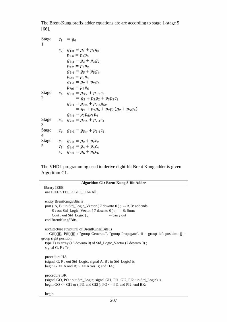
207
The Brent-Kung prefix adder equations are are according to stage 1-stage 5
[66].
Stage
1 𝑐1 = 𝑔0
𝑐2 𝑔1:0 = 𝑔1 + 𝑝1𝑔0
𝑝1:0 = 𝑝1𝑝0
𝑔3:2 = 𝑔3 + 𝑝3𝑔2
𝑝3:2 = 𝑝3𝑝2
𝑔5:4 = 𝑔5 + 𝑝5𝑔4
𝑝5:4 = 𝑝5𝑝4
𝑔7:6 = 𝑔7 + 𝑝7𝑔6
𝑝7:6 = 𝑝7𝑝6 Stage
2 𝑐4 𝑔3:0 = 𝑔3:2 + 𝑝3:2𝑐2
= 𝑔3 + 𝑝3𝑔2 + 𝑝3𝑝2𝑐2
𝑔7:4 = 𝑔7:6 + 𝑝7:6𝑔5:4
= 𝑔7 + 𝑝7𝑔6 + 𝑝7𝑝6(𝑔2 + 𝑝5𝑔4) 𝑔7:4 = 𝑝7𝑝6𝑝5𝑝4
Stage
3 𝑐8 𝑔7:0 = 𝑔7:4 + 𝑝7:4𝑐4
Stage
4 𝑐6 𝑔5:0 = 𝑔5:4 + 𝑝5:4𝑐4
Stage
5 𝑐3
𝑐5
𝑐7
𝑔2:0 = 𝑔2 + 𝑝2𝑐2
𝑔4:0 = 𝑔4 + 𝑝4𝑐4
𝑔6:0 = 𝑔6 + 𝑝6𝑐6
The VHDL programming used to derive eight-bit Brent Kung adder is given
Algorithm C1.
Algorithm C1: Brent Kung 8-Bit Adder
library IEEE;
use IEEE.STD_LOGIC_1164.All;
entity BrentKung8Bits is
port ( A, B : in Std_Logic_Vector ( 7 downto 0 ) ; -- A,B: addends
S : out Std_Logic_Vector ( 7 downto 0 ) ; -- S: Sum;
Cout : out Std_Logic ) ; -- carry out
end BrentKung8Bits ;
architecture structural of BrentKung8Bits is
-- G(ii)(jj), P(ii)(jj) : "group Generate", "group Propagate". ii = group left position, jj =
group right position
type Tr is array (15 downto 0) of Std_Logic_Vector (7 downto 0) ;
signal G, P : Tr ;
procedure HA
(signal G, P : out Std_Logic; signal A, B : in Std_Logic) is
begin G <= A and B; P <= A xor B; end HA;
procedure BK
(signal GO, PO : out Std_Logic; signal GI1, PI1, GI2, PI2 : in Std_Logic) is
begin GO <= GI1 or ( PI1 and GI2 ); PO <= PI1 and PI2; end BK;
begin

208
-- "HA" cells row
HA ( G(07)(07) , P(07)(07) , A(07) , B(07) ) ;
HA ( G(06)(06) , P(06)(06) , A(06) , B(06) ) ;
HA ( G(05)(05) , P(05)(05) , A(05) , B(05) ) ;
HA ( G(04)(04) , P(04)(04) , A(04) , B(04) ) ;
HA ( G(03)(03) , P(03)(03) , A(03) , B(03) ) ;
HA ( G(02)(02) , P(02)(02) , A(02) , B(02) ) ;
HA ( G(01)(01) , P(01)(01) , A(01) , B(01) ) ;
HA ( G(00)(00) , P(00)(00) , A(00) , B(00) ) ;
-- "BK" cells row 1
BK ( G(07)(06) , P(07)(06) , G(07)(07) , P(07)(07) , G(06)(06) , P(06)(06) ) ;
BK ( G(05)(04) , P(05)(04) , G(05)(05) , P(05)(05) , G(04)(04) , P(04)(04) ) ;
BK ( G(03)(02) , P(03)(02) , G(03)(03) , P(03)(03) , G(02)(02) , P(02)(02) ) ;
BK ( G(01)(00) , P(01)(00) , G(01)(01) , P(01)(01) , G(00)(00) , P(00)(00) ) ;
-- "BK" cells row 2
BK ( G(07)(04) , P(07)(04) , G(07)(06) , P(07)(06) , G(05)(04) , P(05)(04) ) ;
BK ( G(03)(00) , P(03)(00) , G(03)(02) , P(03)(02) , G(01)(00) , P(01)(00) ) ;
-- "BK" cells row 3
BK ( G(07)(00) , P(07)(00) , G(07)(04) , P(07)(04) , G(03)(00) , P(03)(00) ) ;
-- "BK" cells row 4
BK ( G(05)(00) , P(05)(00) , G(05)(04) , P(05)(04) , G(03)(00) , P(03)(00) ) ;
-- "BK" cells row 5
BK ( G(02)(00) , P(02)(00) , G(02)(02) , P(02)(02) , G(01)(00) , P(01)(00) ) ;
BK ( G(04)(00) , P(04)(00) , G(04)(04) , P(04)(04) , G(03)(00) , P(03)(00) ) ;
BK ( G(06)(00) , P(06)(00) , G(06)(06) , P(06)(06) , G(05)(00) , P(05)(00) ) ;
-- "XOR" gates row
Cout <= G(07)(00) ;
S(07) <= P(07)(07) xor G(06)(00) ;
S(06) <= P(06)(06) xor G(05)(00) ;
S(05) <= P(05)(05) xor G(04)(00) ;
S(04) <= P(04)(04) xor G(03)(00) ;
S(03) <= P(03)(03) xor G(02)(00) ;
S(02) <= P(02)(02) xor G(01)(00) ;
S(01) <= P(01)(01) xor G(00)(00) ;
S(00) <= P(00)(00) ;
end structural ;
209
References
[1] International Technology Roadmap for Semiconductors (www.itrs.net)
[2] Borkar, S, Thousand Core Chips: A Technology Perspective,
Proceedings of the 44th
annual Design Automation Conference. ACM:
San Diego, California, 2007.
[3] NASA Thesaurus
[4] Normand, E.,Single Event Upset at Ground Level, IEEE Transactions
on Nuclear Science, 1996. 43(6): p. 2742-2750
[5] VideogeniX, SEUs and Their Effects on Electronic Devices: A White
Paper on Why Electronic Equipment Locks Up for No Apparent Reason
and How to Remedy the Situation, 2006
[6] Subahasish Mitra, Ming Zhang, Norbert Seifert, TM Mak and Kee Sup
Kim, Soft Error Resilient System Design through Error Correction,
International Conference on Very Large Scale Integration, IFIP, 2006
[7] T. C. May and M. H. Woods, Alpha-Particle-Induced Soft Errors in
Dynamic Memories, IEEE Trans. Electron Devices, Vol. ED-26, 1979,
pp. 2–8.
[8] C. M. Hsieh, P. C. Murley, and R. R. O’Brien, Dynamics of Charge
Collection from Alpha-Particle Tracks in Integrated Circuits, Proc.
IRPS, 1981, pp. 38–42
[9] J. F. Ziegler and W. A. Lanford, The Effect of Sea Level Cosmic Rays
on Electronic Devices, J. Appl. Phys., Vol. 52, 1981, pp. 4305–4318.
[10] C. A. Gossett, B. W. Hughlock, M. Katoozi, G. S. LaRue, and S. A.
Wender, Single Event Phenomena in Atmospheric Neutron
Environments, IEEE Trans. Nucl. Sci., Vol. 40, Dec. 1993, pp. 1845–
1856
[11] G. R. Srinivason, P. C. Murley, and H. K. Tang, Accurate, Predictive
Modelling of Soft Error Rate Due to Cosmic Rays and Chip Alpha
Radiation, IEEE Proc. IRPS, 1994, pp. 12–16
[12] T. R. Oldham, S. Murrill, and C. T. Self, Single Event Upset of VLSI
Memory Circuits Induced by Thermal Neutrons, Radiation Effects,
Research, and Engineering, Vol. 5, no. 1, 1986, pp. 4–12
[13] R. C. Baumann, T. Z. Hossain, S. Murata, and H. Kitagawa, Boron
Compounds as a Dominant Source of Alpha Particles in Semiconductor
Devices, IEEE Proc. IRPS, 1995, pp. 297–302.
[14] R. C. Baumann, T. Z. Hossain, E. B. Smith, S. Murata, and H.
Kitagawa, Boron as a Primary Source of Radiation in High Density
DRAM’s, IEEE Proc. VLSI Symp., 1995, pp. 81–82.
[15] R. C. Baumann and E. B. Smith, Neutron-Induced Boron Fission as a
Major Source of Soft Errors in Deep Submicron SRAM Devices, IEEE
Proc. IRPS, 2000, pp. 152–157
[16] R. C. Baumann, Soft Errors in Advanced Semiconductor Devices—Part
I: The Three Radiation Sources, IEEE Transactions on Device and
Materials Reliability Vol. 1, No. 1, March 2001.
[17] Tanay Karnik, Peter Hazucha, Jagdish Patel, Characterization of Soft
Errors Caused by Single Event Upsets in CMOS Processes, IEEE
Transactions on Dependable and Secure Computing, Vol 1, Issue: 2,
2004, pp. 128-143.
[18] JEDEC Solid State Technology Association, Measurement and Reporting
of Alpha Particle and Terrestrial Cosmic Ray-Induced Soft Errors in
210
Semiconductor Devices, October 2006
[19] Fan Wang and Vishwani D. Agrawal, Single Event Upset: An
Embedded Tutorial, 21st International Conference on VLSI Design,
2008, pp 429 – 434.
[20] L.Anghel, M.Rebaunger, M.Sonze Reorda and M.Violante, Multi-Level
Fault Effects Evaluation, Radiation Effects on Embedded
Systems,Springer, 2007, pp. 69-88.
[21] R.D. Schrimp, Radiation Effects in Microelectronics, Radiation Effects
on Embedded Systems , Springer, 2007, pp.11-29
[22] Balkaran S.Gill, Chris Papachristou, Francis G.Wolff and Norbert
Seifert, Node Sensitivity Analysis for Soft Errors in CMOS Logic,
International Test Conference, 2005.
[23] A. J. Klein Osowski et al, Modeling Single-Event Upsets in 65-nm
Silicon-on-Insulator Semiconductor Devices, IEEE Transactions on
Nuclear Science, Vol. 53. No. 6, Dec. 2006, pp. 3321-3328
[24] Hungse Cha and Janak H. Patel, A Logic Level Model for Alpha
Particle Hits in CMOS Circuits, International Conference on Computer
Design, October 1993, pp 538-542.
[25] V.A. Carreno and G Choi, R.K Layer, Analog-Digital Simulation of
Transient-Induced Logic Errors and Upset Susceptibility of an
Advanced Control System, NASA Technical Memorondum 4241, Nov
1990
[26] C. Dai et al, Alpha-SER Modelling and Simulation for Sub-0.25μm
CMOS Technology, IEEE Symposium on VLSI Technology, June
1999, pp. 81-82.
[27] Vikas Chandra and Robert Aitken, Impact of Technology and Voltage
Scaling on the Soft Error Susceptibility in Nanoscale CMOS, IEEE
International Symposium on Defect and Fault Tolerance of VLSI
Systems, 2008,pp 114-122. [28] Weidong Kuang, Ibarra C.M and Peiyi Zhao, Soft Error Hardening for
Asynchronous Circuits ,22nd
IEEE International Symposium on Defect
and Fault Tolerance in VLSI Systems, 2007, pp 273-281.
[29] J. Spars ø and S. Furber, Principles Of Asynchronous Circuit Design A
Systems Perspective Kluwer, Academic Publishers, 2001
[30] Singh, M. and S.M. Nowick, MOUSETRAP: Ultra-High-Speed
Transition-Signaling Asynchronous Pipelines, Proceedings of 2001
International Conference on Computer Design, 2001
[31] W.J Bainbridge, S.J Salisbury, Glitch Sensitivity and Defense of Quasi
Delay-Insensitive Network-on-Chip Links , IEEE Symposium on
Asynchronous Circuits and Systems, 2009,pp 35-44.
[32] M. Fazeli, SG Miremadi, A Ejali and A Patooghyi, Low Energy Single
Event Upset/Single Event Transient-Tolerant Latch for Deep
Submicron Technologies, IET Computer Digit Tech, Vol 3, Iss 3, 2009,
pp. 289-303.
[33] Martin Omana, Daniele Rossi and Cecilia Metra, Latch Susceptibility to
Transient Faults and New Hardening Approach, IEE Transactions on
Computer, Vol 56, No 9, 2007, pp. 1255-1268.
[34] Zhao Y and Dey S, Separate Dual-Transistor Registers- A Circuit
Solution for On-Line Testing of Transient Error in UDSM-IC, Proc. 9th
IEEE International On–Line Testing Symposium , 2003, pp. 7-11.
[35] Mitra, S., N. Seifert, M. Zhang, Q. Shi and K.S. Kim, Robust System
Design with Built-In Soft Error Resilience, IEEE Computer, Vol. 38,
211
No. 2, pp. 43-52, Feb. 2005.
[36] Gardiner KT, Yakovlev A and Bystrov A., A C-element Latch Scheme
with Increased Transient Fault Tolerance for Asynchronous Circuits, International On-Line Testing Symposium Proceedings, Heraklion,
Crete, Greece: IEEE Computer Society, 2007.
[37] Y. Monnet, M. Renaudin, and R. Leveugle, Designing Resistant
Circuits Against Malicious Fault Injection Using Asynchronous Logic,
IEEE Transactions on Computers 55(9), September 2006, pp1104–
1115.
[38] Ja Chun Ku and Yehea Ismail, A Compact and Accurate Temperature-
Dependent Model for CMOS Circuit Delay, IEEE International
Symposium on Circuits and Systems, 2007, pp. 3736-3739.
[39] A. Osman, M. Osman, N. Dogan, and M. Imam, An extended tanh law
MOSFET model for high temperature circuit simulation, JSSC, 1995,
pp. 147-150.
[40] Y. Taur and T. Ning, Fundamentals of modern VLSI devices,
Cambridge University Press, 1998
[41] A. Bellaouar, A. Fridi, M. I. Elmasry and K. Itoh, Supply Voltage
Scaling for Temperature Insensitive CMOS Circuit Operation, IEEE
Trans. on Circuits and Systems, Vol. 45, No. 3, March 1998, pp. 415-
417.
[42] K. Roy, S. Mukhopadhyay, and H. Mahmood-Meimand, Leakage
current mechanisms and leakage reduction techniques in deep-
submicrometer CMOS circuits, Proc. IEEE, 2003, pp. 305-327.
[43] Veendrick, H,Short-circuit Dissipation of Static CMOS Circuitry and
its Impact on the Design of Buffer Circuits, Solid-State Circuits, IEEE
Journal of 19(4), 1984, pp 468–473
[44] Neeraj Kr. Shukla et al, Analysis of the Effect of Temperature and Vdd
on Leakage Current in Conventional 6T-SRAM Bit-Cell at 90nm and
65nm Technology, International Journal of Computer Applications, July
2011,Vol 26, No 1 pp. 44-48.
[45] Rajaraman Ramanarayanan, Ramakrishnan Krishnan, Vijaykrishnan
Narayanan and Mary Jane Irwin, Modelling Soft Errors at the Device
and Logic Levels for Combinational Circuits, IEEE Transactions on
Dependable and Secure Computing, Vol 6, No 3, 2009
[46] A. J. Martin, Formal Program Transformations for VLSI Circuit
Synthesis, Formal Development of Programs and Proofs (E. W.
Dijkstra, ed.), UT Year of Program- ming Series, pp. 59-80, Addison-
Wesley, 1989 [47] Tino Heijmen et al, A Comparative Study on the Soft-Error Rate of
Flip-Flop from 90-nm production Libraries, 44th
IEEE International
Symposium on Reliability Physics, March 2006, pp. 204-211.
[48] Kumar, R and Kursun, V, Impact of Temperature Fluctuation on
Circuits Characteristics in 180nm and 65 nm CMOS Technologies,
International Symposium on Circuits and Systems, 2006, pp. 3858-
3861.
[49] I. E. Sutherland, Micropipelines, Communications of the AGM, Vol.
32, pp. 720-738, June 1989
[50] K. van Berkel, Beware the Isochronic Fork, The VLSI journal, Vol. 13,
pp. 103-128, June 1992
[51] M. Shams, J. C. Ebergen, and M. I. Elmasry, Optimizing CMOS
Implementations of the C-element, Proceedings of the 1997 IEEE

212
International Conference on Computer Design: VLSI in Computers and
Processors, pp. 700-705, 1997
[52] Gottfried Fuchs, Matthias Fugger and Andreas Steininger, On the
Threat of Metastability in an Asynchronous Fault-Tolerant Clock
Generation Scheme, Fault-Tolerant Distributed Algorithms on VLSI
Chips.
[53] Ming Zhang and Naresh R Shanbhag, A Soft Error Rate Analysis
(SERA) Methodology, International Conference Computer Aided
Design, pp. 111-118, 2004.
[54] Peter Hazucha and Christer Svensson, Impact of CMOS Technology
Scaling on the Atmospheric Neutron Soft Error Rate, IEEE
Transactions on Nuclear Science, Vol 47, Issue: 6, 2000, pp. 2586-2594
[55] X.W.Zhu and C.R.Cirba,Charge Deposition Modelling of Thermal
Neutron Products in Fast Submicron MOS Devices, IEEE Transactions
on Nuclear Science, Vol 46, No 6, 2006, pp.1378-1385
[56] 0. C. Allkofer and P. K. Grieder, Physics Data: Cosmic Ravs on Earth,
Fachinformationszentm Energie, Physik, Mathematik GmbH,
Karlsruhe, 1984
[57] Moreira, M.T, Oliveira, B.S, Pontes J.J.H, Moraes, F.G, Calazans,
N.L.V, Impact of C-elements in Asynchronous Circuits, International
Symposium on Quality Electronic Design, 2012, pp. 438-444
[58] Dan Ernst, Nam Sung Kim, Shidharta Das, Sanjay Pant, Rajeev Rao
and Toan Pham, Razor, A Low-Power Pipeline Based on Circuit-Level
Timing Speculation, Proceedings of the 36th
International Symposium
on Microarchitecture (MICRO-36’03), 2003, pp. 7-18.
[59] Preeti Verma and R.A Mishra, Temperature Dependence of
Propagation Delay Characteristic in LECTOR based CMOS Circuit,
Special Issue of International Journal of Computer Applications (0975
– 8887) on Electronics, Information and Communication Engineering –
ICEICE No.6, Dec 2011
[60] Kanika Kaur and Arti Noor, Corner and Delay Analysis of Low Power
CMOS Cells, International Journal of Electrical and Electronics
Engineering Research (IJEEER) ISSN 2250-155X, Vol. 3, Issue 1, Mar
2013, 161-168.
[61] F. Hamzaoglu and M. Stan, Circuit-Level Techniques to Control Gate
Leakage for Sub-100 nm CMOS, Proc. Int. Symp. Low Power Design,
2002, pp. 60–63. [62] Ethiopia Nigussie, Juha Plosila, and Jouni Isoaho. Current Mode On-
Chip Interconnect Using Level-Encoded Two-Phase Dual-Rail
Encoding, IEEE International Symposium on Circuits and Systems,
ISCAS 2007, 2007.
[63] Yebin Shi, Fault-Tolerant Delay-Insensitive Communication, Thesis
submitted to the Faculty of Engineering and Physical Science, University of
Manchester, 2010
[64] R. P. Brent and H. T. Kung, A Regular Layout for Parallel Adders,
Computers, IEEE Transactions on, Vol. C-31, 1982, pp. 260-264.
[65] Salah Hasan Ibrahim, Sawal Hamid Md Ali and Md. Shabiul Islam,
High Speed Direct Digital Frequency Synthesizer with Pipelining
Phase Accumulator Based on Brent-Kung Adder, 10th IEEE International
Conference on Semiconductor Electronics (ICSE), 2012.
[66] Wang, N., et al., Characterizing the Effects of Transient Faults on a
High-Performance Processor Pipeline, International Conference
213
Dependable Systems and Networks, 2004, pp. 61-70
[67] I. Koren, Computer Arithmetic Algorithms, Natick, MA: A.K. Peters
Ltd., 2002.