SoC FPGAs: Opportunities and...
84
© 2018 Microsemi, a wholly owned subsidiary of Microchip Technology Inc. 1 SoC FPGAs: Opportunities and Challenges Advanced Workshop on Modern FPGA Based Technology for Scientific Computing Nizar Abdallah May 2019
Transcript of SoC FPGAs: Opportunities and...

© 2018 Microsemi, a wholly owned subsidiary of Microchip Technology Inc. 1
SoC FPGAs: Opportunities and Challenges
Advanced Workshop on Modern FPGA Based Technology for Scientific Computing
Nizar AbdallahMay 2019

2© 2018 Microsemi
▪ A short bio…
▪ What will we be talking about?

3© 2018 Microsemi
Disclaimer–On Our Ability to Predict the Future

4© 2018 Microsemi
Disclaimer–On Our Ability to Predict the Future

5© 2018 Microsemi
Introduction

6© 2018 Microsemi

7© 2018 Microsemi

8© 2018 Microsemi
More Intelligence in Every System

9© 2018 Microsemi
▪ IoT => distributed intelligence & interconnectivity
▪ Data explosion, processing (AI & ML) => computation, response time
▪ Energy needs => decentralized processing at end points + reconfigurability
▪ Environmental sustainability (product as a service) => cloud storage, response time, adaptability
▪ Social sustainability => cost & access
▪ Security => response time
▪ Well being (robotics, medical, comfort) => response time, adaptability, portability
▪ Theoretical research: space exploration => reliability
Society’s Top Challenges and Trends

10© 2018 Microsemi
▪ Everything we do has a digital component
▪ Push to the cloud
▪ Run analytics
▪ Push back to the source
At the Center of the Digital Transformation
Memory FPGA
Inspired from Intel CEO Brian Krzanich, IDF 2016
Cloud &
Data Centers
Things &
Devices

11© 2018 Microsemi
Design Cost
▪ Up to $300M for a new SoC
▪ Between $20M - $50M with reuse
Source: IBS

12© 2018 Microsemi
Performance Improvement Trend

13© 2018 Microsemi
Key Requirements
Cost + Speed + Power + Flexibility
Integration
[Re] Programmability
FPGA SoC

14© 2018 Microsemi
FPGA Economics
Asia-Pacific FPGA market growth. Source: Global Market Insights U.S. FPGA market Growth. Source: Grand View Research

15© 2018 Microsemi
FPGA Basics

16© 2018 Microsemi
Programmable Logic Basics
▪ Flexible architecture with virtually no restrictions – any pin to any logic block. LUT4 + FF = an LE
▪ Large Density, High pin count – SRAM based or Flash
▪ Highly integrated with memory, DSP, transceivers
▪ Variable timing dependent on routing
Field Programmable Gate Array (FPGA) Complex Programmable Logic Device (CPLD)
▪ Less flexible architecture with routing limitations –uses Macrocell blocks to build functions
▪ Low density EEPROM based but with fixed timing
▪ Great for simple logic functions
▪ No investment being made in this technology
17© 2018 Microsemi
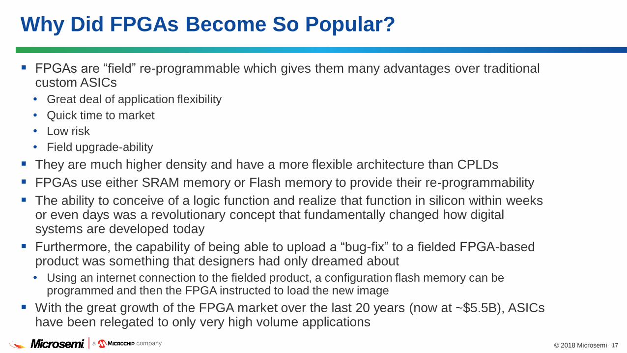
Why Did FPGAs Become So Popular?
▪ FPGAs are “field” re-programmable which gives them many advantages over traditional custom ASICs
• Great deal of application flexibility
• Quick time to market
• Low risk
• Field upgrade-ability
▪ They are much higher density and have a more flexible architecture than CPLDs
▪ FPGAs use either SRAM memory or Flash memory to provide their re-programmability
▪ The ability to conceive of a logic function and realize that function in silicon within weeks or even days was a revolutionary concept that fundamentally changed how digital systems are developed today
▪ Furthermore, the capability of being able to upload a “bug-fix” to a fielded FPGA-based product was something that designers had only dreamed about
• Using an internet connection to the fielded product, a configuration flash memory can be programmed and then the FPGA instructed to load the new image
▪ With the great growth of the FPGA market over the last 20 years (now at ~$5.5B), ASICs have been relegated to only very high volume applications

18© 2018 Microsemi
▪ All FPGAs have some combination of these building blocks and switch matrices
▪ Other blocks that are becoming more popular within FPGAs are
• Transceiver Blocks from 5G to 25G+
• Analog PLLs, crypto processors, DDR controllers, ADCs
• Embedded processors (Arm and RISCV)
FPGA Architecture
4-Input Look-up-table (LUT4) plus FF 20Kbit Large SRAM (LSRAM) 18x18 Multiply Math Block
Routing Switch Matrix
Logic Element
Xilinx/Altera Microchip

19© 2018 Microsemi
How Do FPGAs Work?
▪ The designer describes his design in• RTL (VHDL or Verilog)
• Uses IP blocks (UART or SPI for example)
▪ Simulates the RTL using Modelsim
▪ Synthesizes the design using Synplify from Synopsys• This converts the RTL into an edif netlist
▪ After place and route, timing and power analysis is performed
▪ Programming takes place using a USB dongle to• Program a SPI flash or NAND flash for Xilinx
and Altera
– Once the chip is told to re-program, it “re-boots” itself with the new image
• Program our FPGA directly since the FPGA is flash based (no “boot” prom needed)
BitstreamJTAG
SPI
Single Chip (Flash)
Multiple Chip (SRAM based)
UsersRTL

20© 2018 Microsemi
▪ Top-Down design methodology
[FPGA] Design Methodology
1- Specifications
2- Partitioning
3- Partial Implementation
4- Assemblage
5- Full Implementation
6- System Validation

21© 2018 Microsemi
FPGA Implementation Flow
▪ Simplified FPGA design implementation flow
Design
Entry
Logic
Synthesis
P&R
(Layout)Programming
Verification

22© 2018 Microsemi
System Validation Flow
▪ Simulation
• Bus Functional Model (BFM)
• Mixed language HDL simulation
▪ Hardware Prototype for system validation

23© 2018 Microsemi
Remember Barto's Law
“Every circuit is considered guilty
until proven innocent”

24© 2018 Microsemi
Example of a FPGA Family Table (PolarFire)
Extended Commercial (0⁰C-100⁰C) and Industrial (-40⁰C-100⁰C) Temperature Support for all Die Package Combinations - RoHS only
FeaturesPolarFire FPGA
MPF100 MPF200 MPF300 MPF500
FPGA Fabric
Logic Elements (4LUT + DFF) 109K 192K 300K 481K
Math Blocks (18x18 MACC) 336 588 924 1480
LSRAM Blocks (20 kbit) 352 616 952 1520
uSRAM Blocks (64x12) 1008 1764 2772 4440
Total RAM (Mbits) 7.6 Mbits 13.3 Mbits 20.6 Mbits 33 Mbits
uPROM (kbits) 297 Kbits 297 Kbits 459 Kbits 513 Kbits
User DLL's/PLL's 8 each 8 each 8 each 8 each
High Speed
I/O
250 Mbps -12.7 Gbps Transceiver Lanes 8 16 16 24
PCIe Gen2 Endpoints/Root Ports 2 2 2 2
Total I/O Total User I/O 296 364 512 584
Packaging
Type / Size / Pitch Total User I/O (HSIO / GPIO) GPIO CDRs / XCVRs
FCSG325 (11x11, 11x14.5*, 0.5 mm) 170(84/86) 8/4 170(84/86) 8/4*
FCSG536 (16x16, 0.5 mm) 300(120/180) 15/4 300(120/180) 15/4
FCVG484 (19x19, 0.8 mm) 284(120/164) 14/4 284(120/164)14/4 284(120/164) 14/4
FCG484 (23x23, 1.0 mm) 244(96/148) 13/8 244(96/148) 13/8 244(96/148) 13/8
FCG784 (29x29, 1.0 mm) 364(132/232) 20/16 388(156/232) 20/16 388(156/232) 20/16
FCG1152 (35x35, 1.0 mm) 512(276/236) 24/16 584(324/260) 24/24
Devices in the same package and family type are pin compatible
Additional Temp Grade: Military (-55⁰C-125⁰C) - Leaded packages only

25© 2018 Microsemi
Where FPGAs Fit Within Electronic Systems?
▪ A common application for an FPGA is as an companion chip to a CPU
• Functions could range from interface expansion, to DSP offload algorithms, to motor control, to image processing, to NVDIMM controllers
▪ High-end FPGAs are used in many communications data-path designs
• Microchip FPGAs fit better in the control plane
▪ With the advent of embedded processors on FPGAs, a new class of applications is emerging where the entire System is On a Chip (SOC)
• SmartFusion2 (M3) and Zynq/Cyclone 5 (dual A9 CPUs
▪ Military and Space applications
• Mil Avionics, missile guidance, soldier hand held
• Nasa based space programs and military communications programs
• Higher volume new space applications – RT plastic

26© 2018 Microsemi
Additional Application Examples

27© 2018 Microsemi
SoC FPGA

28© 2018 Microsemi
▪ FPGA• Field Programmable Gate Array
• Plenty of I/O options
• Extremely parallel architecture
• Programmable hardware
▪ SoC• System on Chip
• CPU Core + Peripherals
• Programmable software
▪ SoC FPGA• SoC & FPGA on a single chip
• Connected through on-chip bus
SoC and SoC FPGA

29© 2018 Microsemi
SoC Overview

30© 2018 Microsemi
SoC Overview
Source: Greg Wright - RISC-V Summit December 2018
31© 2018 Microsemi
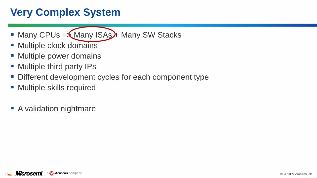
Very Complex System
▪ Many CPUs => Many ISAs + Many SW Stacks
▪ Multiple clock domains
▪ Multiple power domains
▪ Multiple third party IPs
▪ Different development cycles for each component type
▪ Multiple skills required
▪ A validation nightmare

32© 2018 Microsemi
▪ Reduce size => Reduce overall system cost
▪ Increase performance
▪ Lower power consumption
▪ Increase system reliability
▪ Need for special bus interface for a CPU
▪ Need for obscure amount of IOs
▪ Need for extra CPU power for your FPGA
▪ Need for extra FPGA speedup for your CPU functions
Why SoC FPGA?

33© 2018 Microsemi
RISC-V: The Opportunity
Homogenization
• Common base (and frozen)
• Shared frameworks and libraries
• Rich ecosystem (and growing)
Customization
• Mix-and-match extensions
• Domain specific features
• Proprietary extensions
• Freedom in implementing

34© 2018 Microsemi
Instruction Set Architecture (ISA)
Application
OS
Compiler Firmware
CPU I/O
Memory
Digital Circuits
Gates & Transistors
Software
Hardware
Instruction Set Architecture (ISA)

35© 2018 Microsemi
Instruction Set Architecture (ISA)
▪ A well-defined hardware/software interface
▪ The “contract” between software and hardware
• Functional definition of operations, modes, and storage locations supported by hardware
• Precise description of how to invoke, and access them
▪ Not in the “contract”: non-functional aspects
• How operations are implemented
• Which operations are fast and which are slow and when
• Which operations take more power and which take less

36© 2018 Microsemi
Instruction Set Architecture (ISA)
HARDWARE
Interface
SOFTWARE
“Contract”
Hardware team
Software team

37© 2018 Microsemi
Why RISC-V for a SoC FPGA?
▪ The RISC-V ISA is Open. Open ISAs allow for …• Low cost migration to ASICs, royalty free usage
• Innovation for custom architectures – free “architectural license” doesn’t restrict usage to fixed architectures
▪ The RISC-V ISA is simple. Simplicity …• Allows for a low power implementation
• Lower cost of ownership - easier to learn, customize and debug
• Simple architectures are easier to secure against threats
Open, Lowest Power, Cost Optimized, Programmable SoC

38© 2018 Microsemi
▪ Consider the following scenarios:
1. The existing design uses an FPGA and a separate microprocessor?• Comparable functionality and performance, but lower board space, power, and cost by as
much as 50% less
2. The current generation uses a proprietary ASIC that includes a microprocessor?• No expensive mask charges or minimum purchase requirements
• Faster time to market with lower risk
• Adapt to changing markets requirements and emerging standards
3. A microprocessor being used today, but would benefit from a peripheral set more tailored to the application?• If forced to accept compromises due to the lack of off-the-shelf processor derivatives
• The design can be differentiated both in hardware and software, making it more difficult for competitors to copy or emulate
When does it make sense?

39© 2018 Microsemi
In Any Case…
Architecture Matters

40© 2018 Microsemi
▪ Design considerations & engineering trade-off decisions
▪ The selection criteria centers on the following areas:• Existing ecosystem (legacy IPs, Software…)
• System performance
• System reliability
• System flexibility
• System cost
• Power consumption
• Continuity (product roadmap)
• Quality of the software solution (development tools)
Criteria for Choosing an SoC FPGA

41© 2018 Microsemi
▪ Industrial Example: Motor Control• The processing must be deterministic (i.e. complete within a given window in time, every time)
System Performance

42© 2018 Microsemi
▪ The processor performance
▪ The fabric performance
▪ The interconnect between fabric and processor
▪ Memory bandwidth
System Performance

43© 2018 Microsemi
System PerformanceThe interconnect between fabric and processor
FPGA Logic
SerDes Channels
SECDED
Memory Interface
Hardened
MCU
SEU-Free
Flash FPGA
Configuration
Memory
Encryption,
Error Detection
And Low Power
Control
SEU Protected
SRAM Blocks
Data transfer between the memory, FPGA fabric, processor, and peripherals

44© 2018 Microsemi
▪ Question: Does the interconnect support high throughput path?
System PerformanceThe interconnect between fabric and processor

45© 2018 Microsemi
▪ If needed, a low latency non-blocking bridge for allowing control access to the FPGA
System PerformanceThe interconnect between fabric and processor

46© 2018 Microsemi
▪ Hardware acceleration example: When the acceleration results are needed by the processor
▪ In this case, in the other direction: Does the architecture include an Accelerator Coherency Port (ACP)?
• ARM Cortex-A9-based SoC FPGAs include a feature called an Accelerator Coherency Port (ACP). Through the ACP, new data produced by an FPGA-based hardware accelerator is transferred directly to the processor’s L2 cache via a low-latency direct connection—not just quickly but coherently
System PerformanceThe interconnect between fabric and processor

47© 2018 Microsemi
▪ Memory controllers are as important as the memory speed
▪ Question: Do you have separate hard memory controllers?
▪ Question: How smart is the memory controller?
System PerformanceMemory bandwidth
17% Faster using a smarter scheduling
algorithm (e.g. deficit weight round robin)

48© 2018 Microsemi
▪ Supporting ECC Memory for content protection• On-Chip RAM
• External DDR Memory Controller
• L1 Cache & L2 Cache
• SPI Controller
• DMA Controller
• 10/100/1G Ethernet Controller
• USB 2.0 OTG Controller
• …
▪ Protection for shared memory• Arm has the concept of “trust zone”
System Reliability

49© 2018 Microsemi
▪ Extending the flexibility to the system level
System Flexibility

50© 2018 Microsemi
▪ Extending the flexibility to the system level
System Flexibility

51© 2018 Microsemi
▪ Extending the flexibility to the system level
System Flexibility

52© 2018 Microsemi
▪ Design considerations & engineering trade-off decisions
▪ The selection criteria centers on the following areas:• Existing ecosystem (legacy IPs, Software…)
• System performance
• System reliability
• System flexibility
• System cost
• Power consumption
• Continuity (product roadmap)
• Quality of the software solution (development tools)
Criteria for Choosing an SoC FPGA

53© 2018 Microsemi
PolarFire SoC FPGA Architecture
Mi-V: Microsemi’s RISC-V Processor

54© 2018 Microsemi
PolarFire SoC FPGA
Industry’s First RISC-V SoC FPGA Architecture Brings Real-Time to Linux, Giving Developers the Freedom to Innovate in Low-Power, Secure and Reliable Designs
▪ First SoC FPGA with deterministic, coherent CPU cluster and a deterministic L2 memory subsystem enabling Linux + real-time applications
▪ First SoC FPGA architecture integrating a RISC-V processor subsystem and low-power FPGA technology
▪ PolarFire SoC FPGA with a mid-range low-power SoC FPGA and high levels of security and reliability

55© 2018 Microsemi
Freedom to implement RISC-V in hardware

56© 2018 Microsemi
Award Winning PolarFire FPGA as an SoC platform
Control Plane
Signal Processing
Video & Image
Processing Hardware
Acceleration
10G Bridging &
Aggregation
Low Power Optics
Portable
Equipment
▪ Proven Security
• Defense-grade security
• DPA safe Crypto coprocessor
• Built-in anti-tamper
▪ Exceptional Reliability
• SEU immune configuration
• Block RAM with ECC
• Extended temperatures
▪ Lowest Power
• Low static power technology
• Power optimized transceivers
• Up to 50% lower than SRAM FPGAs

57© 2018 Microsemi
Low Power MSS
✓ Low power RISC-V micro-architecture
✓ 2MB L2 cache: increases cache hit/miss ratio
✓ 0.5-0.9W lower power
✓ Power-optimized transceivers
Low Power: RISC-V MSS vs. Alternatives
0.0
200.0
400.0
600.0
800.0
1000.0
1200.0
1400.0
1600.0
PolarFireSoC Zynq Zynq+
Processor Power4000 DMIPS load, DDR@32b x 1600Mb/s
DDR
ProcessorDynamic
ProcessorStatic
Comp A
22nm
Comp A
16nmPolarFire SOC
28nm
0
2
4
6
8
10
12
14
16
PolarFireSoC Zynq Zynq+
4x4x60MHz DFE Power
Static
XCVR
lProcessor
Dynamic
4x4x60MHz RRH
368MHz
732DSP
126k LE
10xCPRI7 1x12.5G
JESD
4000 DMIPS
4GB/s
DDR
Comp A
22nm
Comp A
16nmPolarFire SOC
28nm
LTE Digital Front End Application
✓ 3-7W lower power for 60MHz 4x4 MIMO implementation

58© 2018 Microsemi
▪ PolarFire SoC inherits best in class PolarFire FPGA Security• DPA resistant bitstream programming
• Anti-tamper
• Cryptographical bound supply chain assurance
• Physically unclonable function
• True random number generator
• Side channel resistant crypto coprocessor
▪ PolarFire SoC has:+ Secure Boot
+ Spectre and Meltdown immunity
+ Physical memory protection
+ SECDED on all memories(single-error correction and double-error detection)
Security Ready for IoT

59© 2018 Microsemi
Real-time Linux?
▪ Wide spread Linux adoption
• Rich OS with thousands of applications to choose from
▪ Requirements still exist for real-time while running Linux
• Safety critical
– The ability to deterministically monitor the execution environment.
• Real-time system control
– Completing tasks deterministically, on time every time.
• Securing the IoT
– Execute a trusted execution environment deterministically for consistent results.
▪ Working with
• We have been able to architect a complex SoC FPGA that provides
– Determinism and a rich OS within the same multi-core CPU cluster

60© 2018 Microsemi
Variable Execution Time in Typical Application Processors
SMP 1
L2
DDR4
CPU
SMP 2
CPU
SMP 3
CPU
SMP 4
CPU
5332800
5333000
5333200
5333400
5333600
5333800
5334000
5334200
Execution Time Variability
Branch predictors, cache misses and lack of coherency affect determinism negatively

61© 2018 Microsemi
▪ Turn off the CPU branch predictors
Solution
SMP 1RT
BP Off
E51 U54
SMP 2
U54
SMP 3
U54
SMP 4
U54

62© 2018 Microsemi
▪ Turn off the CPU branch predictors
▪ Make sure all cores coherent to the memory subsystem
Solution
SMP 1
L2
DDR4
RT
BP Off
E51 U54
SMP 2
U54
SMP 3
U54
SMP 4
U54

63© 2018 Microsemi
▪ Turn off the CPU branch predictors
▪ Make sure all cores coherent to the memory subsystem
▪ Make the memory system deterministic
Solution
SMP 1
L2
DDR4
RT
BP Off
E51 U54
SMP 2
U54
SMP 3
U54
SMP 4
U54
Direct
Access

64© 2018 Microsemi
▪ Turn off the CPU branch predictors
▪ Make sure all cores coherent to the memory subsystem
▪ Make the memory system deterministic
▪ Share coherent memory for message passing
Solution
SMP 1
L2
DDR4
RT
BP Off
E51 U54
SMP 2
U54
SMP 3
U54
SMP 4
U54
Direct
AccessCoherent
Buffers

65© 2018 Microsemi
▪ Turn off the CPU branch predictors
▪ Make sure all cores coherent to the memory subsystem
▪ Make the memory system deterministic
▪ Share coherent memory for message passing
▪ Linux and real time in a coherent memory subsystem
Solution
SMP 1
L2
DDR4
RT
BP Off
E51 U54
SMP 2
U54
SMP 3
U54
SMP 4
U54
Direct
AccessCoherent
Buffers
5722600
5722800
5723000
5723200
5723400
5723600
5723800
5724000
No Execution Time Variability
RESULT

66© 2018 Microsemi
PolarFire SoC - RISC-V enabled innovation platform
Freedom to Innovate in
• Linux and Real-Time
• Securely Connected IoT systems
• High-Rel Safety Critical Systems
• Thermal and Power Constrained Systems

67© 2018 Microsemi
PolarFire SoC Summary
▪ PolarFire FPGA Award Winning Features
• 30-50% Lower power
• Defense grade security
• Exceptional reliability
• Smallest, lowest power, secure form factors – 11x11, 16x16, 19x19
▪ PolarFire Microprocessor Subsystem
• Linux and real time in a deterministic, coherent CPU cluster
• 30-50% Lower power
• Defense grade secure boot
• Spectre/Meltdown immune
• SECDED on all memories

68© 2018 Microsemi
▪ Free Rapid Software Development and Debug Capabilities Without Hardware
▪ Complete PolarFire SoC Processor Subsystem Model
▪ Available now!
Freedom to start software development

69© 2018 Microsemi
HiFive Unleashed Development BoardHiFive Unleashed Expansion Board
PolarFire SoC Embedded Experts Development Kit
Freedom to begin hardware development

70© 2018 Microsemi
New Mi-V Embedded Experts Network
Freedom to engage with the Mi-V Ecosystem

71© 2018 Microsemi
RISC-V CPUs
RISC-V Soft CPU LE'S CoreMark Score Cache Size Mul/Div Floating Point Availability
CORE_RISCV_AXI4* 10K 2.01 8K I and D Yes N/A Now
Mi_V_RV32IMAF_L1_AHB* 26K 2.01 8K I and D Yes Single Precision Now
Mi_V_RV32IMA_L1_AHB* 10K 2.01 8K I and D Yes N/A Now
Mi_V_RV32IMA_L1_AXI* 10K 2.01 8K I and D Yes N/A Now
*Click the RISC-V Soft CPU to download the Handbook

72© 2018 Microsemi
Summary
▪ PolarFire SoC gives designers the freedom to create innovative low power systems by enabling Linux and deterministic architectures in novel ways
• First SoC FPGA with deterministic, coherent CPU cluster and a deterministic L2 memory subsystem enabling Linux + real-time applications
• First SoC FPGA architecture integrating a RISC-V processor subsystem and low-power FPGA technology
• PolarFire SoC addresses the industry’s need for a mid-range low-power SoC FPGA with high levels of security and reliability
▪ Developers can begin development today• antmicro Renode platform for software development
• PolarFire SoC Embedded Experts Development Kit for hardware development
• New Mi-V Embedded Experts Network

73© 2018 Microsemi
PolarFire Dual Camera Video Kit
Example using a soft RISC-V

74© 2018 Microsemi
Imaging and Video Solutions for Smart Embedded Vision
▪ Based on PolarFire™
▪ Ideal for mid-bandwidth(4K/2K) imaging/video
▪ Up to 50 percent lower power compared to SRAM-based FPGAs
▪ Target Applications
• Machine learning
• Automotive
• Surveillance
• Medical imaging

75© 2018 Microsemi

76© 2018 Microsemi

77© 2018 Microsemi
Board Components and Operations
▪ PF_Dual_Camera_Video_Kit_Demo\Microsemi_PolarFire_FPGA_Video_Kit_User_Guide_UG0856_V1.pdf

78© 2018 Microsemi

79© 2018 Microsemi
How do you make a design with a Mi-V

80© 2018 Microsemi
How do you make a design with a Mi-V
▪ The design suite is called Libero SoC
▪ You can run through a full design flow, from synthesis to programming your device
▪ Libero includes the firmware catalog to create drivers for IP cores

81© 2018 Microsemi
How do you write a program and run it on the Mi-V
▪ Softconsole Eclipse IDE required for the development
▪ Runs on Windows and Linux
▪ Eclipse-based IDE (Integrated Development Environment)
▪ Uses OpenOCD and GDB for debugging
▪ Comes bundled with several sample projects
▪ Most common demo is called “Blinky” which demos UART, GPIO and Interrupts
▪ If running correctly, the LEDs on the device should blink on and off, and when the project is first run, it will send a “hello” message over UART
▪ Softconsole has a built-in terminal emulator
▪ Resources at github.com/riscv-on-Microsemi-fpga

82© 2018 Microsemi

83© 2018 Microsemi
Another Example (ASIC Design Services)

84© 2018 Microsemi
Another Example (ASIC Design Services)
▪ PolarFire + Mi-V in Tiny Yolo Video