SFP+ Optical Transceivers,Fiber Optic Transceivers,Fiber ...

DE
RE
R
6
7
3
1
2
B
A
Bus
D4
Product
Folder
Sample &Buy
Technical
Documents
Tools &
Software
Support &Community
SN65176B, SN75176BSLLS101F –JULY 1985–REVISED JANUARY 2015
SNx5176B Differential Bus Transceivers1 Features 3 Description
The SN65176B and SN75176B differential bus1• Bidirectional Transceivers
transceivers are designed for bidirectional data• Meet or Exceed the Requirements of ANSI communication on multipoint bus transmission lines.Standards TIA/EIA-422-B and TIA/EIA-485-A They are designed for balanced transmission linesand ITU Recommendations V.11 and X.27 and meet ANSI Standards TIA/EIA-422-B and
TIA/EIA-485-A and ITU Recommendations V.11 and• Designed for Multipoint Transmission onX.27.Long Bus Lines in Noisy Environments
• 3-State Driver and Receiver Outputs The SN65176B and SN75176B devices combine a 3-state differential line driver and a differential input line• Individual Driver and Receiver Enablesreceiver, both of which operate from a single 5-V• Wide Positive and Negative Input/Output Bus power supply. The driver and receiver have active-Voltage Ranges high and active-low enables, respectively, that can be
• ± 60-mA Max Driver Output Capability connected together externally to function as adirection control. The driver differential outputs and• Thermal Shutdown Protectionthe receiver differential inputs are connected• Driver Positive and Negative Current Limiting internally to form differential input/output (I/O) bus
• 12-kΩ Min Receiver Input Impedance ports that are designed to offer minimum loading tothe bus when the driver is disabled or VCC = 0. These• ± 200-mV Receiver Input Sensitivityports feature wide positive and negative common-• 50-mV Typ Receiver Input Hysteresismode voltage ranges, making the device suitable for• Operate From Single 5-V Supply party-line applications.
The driver is designed for up to 60 mA of sink or2 Applicationssource current. The driver features positive and
• Chemical/Gas Sensors negative current limiting and thermal shutdown for• Digital Signage protection from line-fault conditions. Thermal
shutdown is designed to occur at a junction• HMI (Human Machine Interfaces)temperature of approximately 150°C. The receiver• Motor Controls: AC Induction, Brushed and Brush- features a minimum input impedance of 12 kΩ, an
less DC, Low- and High-Voltage, Stepper Motors, input sensitivity of ±200 mV, and a typical inputand Permanent Magnets hysteresis of 50 mV.
• TETRA Base StationsDevice Information(1)
• Telecom Towers: Remote Electrical Tilt UnitsPART NUMBER PACKAGE (PIN) BODY SIZE (NOM)(RET) and Tower Mounted Amplifiers (TMA)
SOIC (8) 4.90 mm × 3.91 mm• Weigh ScalesSNx5176 PDIP (8) 9.81 mm × 6.35 mm• Wireless Repeaters
SOP (8) 6.20 mm × 5.30 mm
(1) For all available packages, see the orderable addendum atthe end of the datasheet.
4 Simplified Schematic
1
An IMPORTANT NOTICE at the end of this data sheet addresses availability, warranty, changes, use in safety-critical applications,intellectual property matters and other important disclaimers. PRODUCTION DATA.

SN65176B, SN75176BSLLS101F –JULY 1985–REVISED JANUARY 2015 www.ti.com
Table of Contents9.2 Functional Block Diagram ....................................... 121 Features .................................................................. 19.3 Feature Description................................................. 122 Applications ........................................................... 19.4 Device Functional Modes........................................ 133 Description ............................................................. 1
10 Application and Implementation........................ 144 Simplified Schematic............................................. 110.1 Application Information.......................................... 145 Revision History..................................................... 210.2 Typical Application ............................................... 146 Pin Configuration and Functions ......................... 310.3 System Examples ................................................. 157 Specifications......................................................... 4 11 Power Supply Recommendations ..................... 167.1 Absolute Maximum Ratings ...................................... 4
12 Layout................................................................... 167.2 Recommended Operating Conditions....................... 412.1 Layout Guidelines ................................................. 167.3 Thermal Information .................................................. 412.2 Layout Example .................................................... 167.4 Electrical Characteristics – Driver ............................. 5
13 Device and Documentation Support ................. 167.5 Electrical Characteristics – Receiver ........................ 613.1 Related Links ........................................................ 167.6 Switching Characteristics – Driver ............................ 613.2 Trademarks ........................................................... 167.7 Switching Characteristics – Receiver........................ 613.3 Electrostatic Discharge Caution............................ 167.8 Typical Characteristics .............................................. 713.4 Glossary ................................................................ 168 Parameter Measurement Information .................. 9
14 Mechanical, Packaging, and Orderable9 Detailed Description ............................................ 12 Information ........................................................... 169.1 Overview ................................................................. 12
5 Revision History
Changes from Revision E (January 2014) to Revision F Page
• Added Applications, Device Information table, Pin Functions table, ESD Ratings table, Thermal Information table,Feature Description section, Device Functional Modes, Application and Implementation section, Power SupplyRecommendations section, Layout section, Device and Documentation Support section, and Mechanical,Packaging, and Orderable Information section. ..................................................................................................................... 1
• Moved Typical Characteristics inside of the Specifications section. ...................................................................................... 7
Changes from Revision D (April 2003) to Revision E Page
• Updated document to new TI data sheet format - no specification changes. ........................................................................ 1• Deleted Ordering Information table. ....................................................................................................................................... 1• Added ESD warning. ............................................................................................................................................................ 16
2 Submit Documentation Feedback Copyright © 1985–2015, Texas Instruments Incorporated
Product Folder Links: SN65176B SN75176B

1
2
3
4
8
7
6
5
R
RE
DE
D
VCC
B
A
GND
SN65176B, SN75176Bwww.ti.com SLLS101F –JULY 1985–REVISED JANUARY 2015
6 Pin Configuration and Functions
Top View
Pin FunctionsPIN
TYPE DESCRIPTIONNAME NO.R 1 O Logic Data Output from RS-485 ReceiverRE 2 I Receive Enable (active low)DE 3 I Driver Enable (active high)D 4 I Logic Data Input to RS-485 DriverGND 5 — Device Ground PinA 6 I/O RS-422 or RS-485 Data LineB 7 I/O RS-422 or RS-485 Data LineVCC 8 — Power Input. Connect to 5-V Power Source.
Copyright © 1985–2015, Texas Instruments Incorporated Submit Documentation Feedback 3
Product Folder Links: SN65176B SN75176B
SN65176B, SN75176BSLLS101F –JULY 1985–REVISED JANUARY 2015 www.ti.com
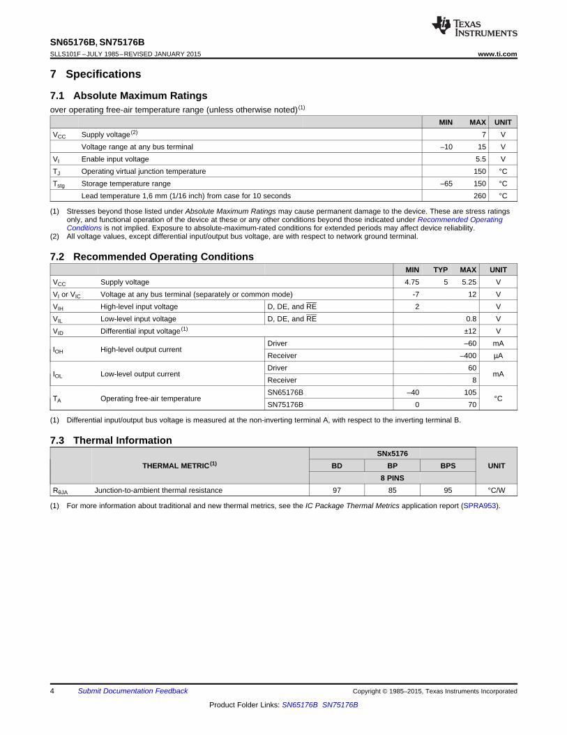
7 Specifications
7.1 Absolute Maximum Ratingsover operating free-air temperature range (unless otherwise noted) (1)
MIN MAX UNITVCC Supply voltage (2) 7 V
Voltage range at any bus terminal –10 15 VVI Enable input voltage 5.5 VTJ Operating virtual junction temperature 150 °CTstg Storage temperature range –65 150 °C
Lead temperature 1,6 mm (1/16 inch) from case for 10 seconds 260 °C
(1) Stresses beyond those listed under Absolute Maximum Ratings may cause permanent damage to the device. These are stress ratingsonly, and functional operation of the device at these or any other conditions beyond those indicated under Recommended OperatingConditions is not implied. Exposure to absolute-maximum-rated conditions for extended periods may affect device reliability.
(2) All voltage values, except differential input/output bus voltage, are with respect to network ground terminal.
7.2 Recommended Operating ConditionsMIN TYP MAX UNIT
VCC Supply voltage 4.75 5 5.25 VVI or VIC Voltage at any bus terminal (separately or common mode) -7 12 VVIH High-level input voltage D, DE, and RE 2 VVIL Low-level input voltage D, DE, and RE 0.8 VVID Differential input voltage (1) ±12 V
Driver –60 mAIOH High-level output current
Receiver –400 µADriver 60
IOL Low-level output current mAReceiver 8SN65176B –40 105
TA Operating free-air temperature °CSN75176B 0 70
(1) Differential input/output bus voltage is measured at the non-inverting terminal A, with respect to the inverting terminal B.
7.3 Thermal InformationSNx5176
THERMAL METRIC (1) BD BP BPS UNIT8 PINS
RθJA Junction-to-ambient thermal resistance 97 85 95 °C/W
(1) For more information about traditional and new thermal metrics, see the IC Package Thermal Metrics application report (SPRA953).
4 Submit Documentation Feedback Copyright © 1985–2015, Texas Instruments Incorporated
Product Folder Links: SN65176B SN75176B

SN65176B, SN75176Bwww.ti.com SLLS101F –JULY 1985–REVISED JANUARY 2015
7.4 Electrical Characteristics – Driverover recommended ranges of supply voltage and operating free-air temperature (unless otherwise noted)
PARAMETER TEST CONDITIONS (1) MIN TYP (2) MAX UNITVIK Input clamp voltage II = –18 mA –1.5 VVO Output voltage IO = 0 0 6 V|VOD1| Differential output voltage IO = 0 1.5 3.6 6 V
RL = 100 Ω, see Figure 10 ½ VOD1 or 2 (3)|VOD2| Differential output voltage V
RL = 54 Ω, see Figure 10 1.5 2.5 5VOD3 Differential output voltage See (4) 1.5 5 V
Change in magnitude of∆|VOD| RL = 54 Ω or 100 Ω, see Figure 10 ±0.2 Vdifferential output voltage (5)
VOC Common-mode output voltage RL = 54 Ω or 100 Ω, see Figure 10 -1 +3 VChange in magnitude of
∆|VOC| common-mode output RL = 54 Ω or 100 Ω, see Figure 10 ±0.2 Vvoltage (5)
VO = 12 V 1IO Output current Output disabled (6) mA
VO = –7 V –0.8IIH High-level input current VI = 2.4 V 20 µAIIL Low-level input current VI = 0.4 V –400 µA
VO = –7 V –250VO = 0 –150
IOS Short-circuit output current mAVO = VCC 250VO = 12 V 250
Outputs enabled 42 70ICC Supply current (total package) No load mA
Outputs disabled 26 35
(1) The power-off measurement in ANSI Standard TIA/EIA-422-B applies to disabled outputs only and is not applied to combined inputs andoutputs.
(2) All typical values are at VCC = 5 V and TA = 25°C.(3) The minimum VOD2 with a 100-Ω load is either ½ VOD1 or 2 V, whichever is greater.(4) See ANSI Standard TIA/EIA-485-A, Figure 3.5, Test Termination Measurement 2.(5) Δ|VOD| and Δ|VOC| are the changes in magnitude of VOD and VOC, respectively, that occur when the input is changed from a high level
to a low level.(6) This applies for both power on and off; refer to ANSI Standard TIA/EIA-485-A for exact conditions. The TIA/EIA-422-B limit does not
apply for a combined driver and receiver terminal.
Copyright © 1985–2015, Texas Instruments Incorporated Submit Documentation Feedback 5
Product Folder Links: SN65176B SN75176B

SN65176B, SN75176BSLLS101F –JULY 1985–REVISED JANUARY 2015 www.ti.com
7.5 Electrical Characteristics – Receiverover recommended ranges of common-mode input voltage, supply voltage, and operating free-air temperature (unlessotherwise noted)
PARAMETER TEST CONDITIONS MIN TYP (1) MAX UNITVIT+ Positive-going input threshold voltage VO = 2.7 V, IO = –0.4 mA 0.2 VVIT– Negative-going input threshold voltage VO = 0.5 V, IO = 8 mA –0.2 (2) VVhys Input hysteresis voltage (VIT+ – VIT–) 50 mVVIK Enable Input clamp voltage II = –18 mA –1.5 VVOH High-level output voltage VID = 200 mV, IOH = –400 µA, see Figure 11 2.7 VVOL Low-level output voltage VID = –200 mV, IOL = 8 mA, see Figure 11 0.45 VIOZ High-impedance-state output current VO = 0.4 V to 2.4 V ±20 µA
VI = 12 V 1II Line input current Other input = 0 V (3) mA
VI = –7 V –0.8IIH High-level enable input current VIH = 2.7 V 20 µAIIL Low-level enable input current VIL = 0.4 V –100 µArI Input resistance VI = 12 V 12 kΩIOS Short-circuit output current –15 –85 mA
Outputs enabled 42 55ICC Supply current (total package) No load mA
Outputs disabled 26 35
(1) All typical values are at VCC = 5 V, TA = 25°C.(2) The algebraic convention, in which the less positive (more negative) limit is designated minimum, is used in this data sheet for common-
mode input voltage and threshold voltage levels only.(3) This applies for both power on and power off. Refer to EIA Standard TIA/EIA-485-A for exact conditions.
7.6 Switching Characteristics – DriverVCC = 5 V, RL = 110 Ω, TA = 25°C (unless otherwise noted)
PARAMETER TEST CONDITIONS MIN TYP MAX UNITtd(OD) Differential-output delay time RL = 54 Ω, see Figure 12 15 22 nstt(OD) Differential-output transition time RL = 54 Ω, see Figure 12 20 30 nstPZH Output enable time to high level See Figure 13 85 120 nstPZL Output enable time to low level See Figure 14 40 60 nstPHZ Output disable time from high level See Figure 13 150 250 nstPLZ Output disable time from low level See Figure 14 20 30 ns
7.7 Switching Characteristics – ReceiverVCC = 5 V, CL = 15 pF, TA = 25°C
PARAMETER TEST CONDITIONS MIN TYP MAX UNITtPLH Propagation delay time, low- to high-level output 21 35
VID = 0 to 3 V, see Figure 15 nstPHL Propagation delay time, high- to low-level output 23 35tPZH Output enable time to high level 10 20
See Figure 16 nstPZL Output enable time to low level 12 20tPHZ Output disable time from high level 20 35
See Figure 16 nstPLZ Output disable time from low level 17 25
6 Submit Documentation Feedback Copyright © 1985–2015, Texas Instruments Incorporated
Product Folder Links: SN65176B SN75176B

4
3
2
1
100806040200–200
120
5
TA – Free-Air Temperature – C°
–40
VCC = 5 V
VID = 200 mV
IOH = –440 Aµ
VO
H–
Hig
h-L
evelO
utp
ut
Vo
ltag
e–
VVO
H
4.5
3.5
2.5
1.5
0.5
TA = 25°C
VCC = 5 V
0.5
0.4
0.3
0.2
0.1
2520151050
30
0.6
IOL – Low-Level Output Current – mA
0
VO
L–
Lo
w-L
evelO
utp
ut
Vo
ltag
e–
VV
OL
–25
VCC = 5.25 V
VCC = 5 V
VCC = 4.75 V
0 –10 –20 –30 –40 –50
5
0
1
2
3
4
IOH – High-Level Output Current – mA
VO
H–
Hig
h-L
evelO
utp
ut
Vo
ltag
e–
VVO
H
4.5
3.5
2.5
1.5
0.5
–5 –15 –35 –45
VID = 0.2 V
TA = 25°C
VO
D–
Dif
fere
nti
alO
utp
ut
Vo
ltag
e–
V 3.5
3
2.5
2
1.5
1
0.5
9080706050403020100
100
4
IO – Output Current – mA
0
VO
D
VCC = 5 V
TA = 25°C
VO
H–
Hig
h-L
evelO
utp
ut
Vo
ltag
e–
V
VCC = 5 V
4.5
4
3.5
3
2.5
2
1.5
1
0.5
–100–80–60–40–200
–120
5
IOH – High-Level Output Current – mA
0
VO
H
TA = 25°C
VCC = 5 V
TA = 25°C
IOL – Low-Level Output Current – mA
0 12020 40 60 80 100
5
0
0.5
1
1.5
2
2.5
3
3.5
4
4.5
–L
ow
-Le
ve
lO
utp
ut
Vo
lta
ge
–V
VO
L
SN65176B, SN75176Bwww.ti.com SLLS101F –JULY 1985–REVISED JANUARY 2015
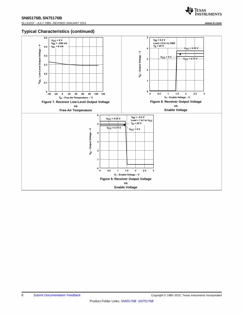
7.8 Typical Characteristics
Figure 1. Driver High-Level Output Voltage Figure 2. Driver Low-Level Output Voltagevs vs
High-Level Output Current Low-Level Output Current
Figure 3. Driver Differential Output Voltage Figure 4. Receiver High-Level Output Voltagevs vs
Output Current High-Level Output Current
Only the 0°C to 70°C portion of the curve applies to theOnly the 0°C to 70°C portion of the curve applies to theSN75176B device.SN75176B device.
Figure 6. Receiver Low-Level Output VoltageFigure 5. Receiver High-Level Output Voltagevsvs
Low-Level Output CurrentFree-Air Temperature
Copyright © 1985–2015, Texas Instruments Incorporated Submit Documentation Feedback 7
Product Folder Links: SN65176B SN75176B
VO
–O
utp
ut
Vo
lta
ge
–V
5
4
3
2
1
2.521.510.50
3
6
VI – Enable Voltage – V
0
VO
Load = 1 kΩ to VCC
VCC = 5 V
VCC = 5.25 V
TA = 25°C
VID = –0.2 V
VCC = 4.75 V
VO
L–
Lo
w-L
evelO
utp
ut
Vo
ltag
e–
V
VID = –200 mV
VCC = 5 V
TA – Free-Air Temperature – C°
0.6
0
0.1
0.2
0.3
0.4
0.5
100806040200–20 120–40
VO
L
IOL = 8 mA
VO
–O
utp
ut
Vo
lta
ge
–V
VCC = 5 V
VCC = 5.25 VTA = 25°C
VID = 0.2 V
0
VI – Enable Voltage – V
30.5 1 1.5 2 2.5
4
3
2
1
0
5
VO
Load = 8 kΩ to GND
VCC = 4.75 V
SN65176B, SN75176BSLLS101F –JULY 1985–REVISED JANUARY 2015 www.ti.com
Typical Characteristics (continued)
Figure 8. Receiver Output VoltageFigure 7. Receiver Low-Level Output Voltagevsvs
Enable VoltageFree-Air Temperature
Figure 9. Receiver Output Voltagevs
Enable Voltage
8 Submit Documentation Feedback Copyright © 1985–2015, Texas Instruments Incorporated
Product Folder Links: SN65176B SN75176B

VOLTAGE WAVEFORMS
tPHZ
1.5 V
2.3 V
0.5 V0 V
3 V
tPZH
Output
Input 1.5 VS1
0 V or 3 V
Output
CL = 50 pF
(see Note A)
TEST CIRCUIT
50 Ω
VOH
Voff ≈0 V
RL = 110 Ω
Generator
(see Note B)
3 V
VOLTAGE WAVEFORMS
tt(OD)
td(OD)
1.5 V
10%
tt(OD)
≈2.5 V
≈–2.5 V
90%50%Output
td(OD)
0 V
3 V
1.5 VInput
TEST CIRCUIT
Output
CL = 50 pF
(see Note A)
50 Ω
RL = 54 ΩGenerator
(see Note B)50%10%
ID
VOL
VOH
–IOH+IOL
2
RL
VOD2
VOC2
RL
SN65176B, SN75176Bwww.ti.com SLLS101F –JULY 1985–REVISED JANUARY 2015
8 Parameter Measurement Information
Figure 10. Driver VOD and VOC
Figure 11. Receiver VOH and VOL
A. CL includes probe and jig capacitance.B. The input pulse is supplied by a generator having the following characteristics: PRR ≤1 MHz, 50% duty cycle, tr ≤ 6
ns, tf ≤ 6 ns, ZO = 50 Ω.
Figure 12. Driver Test Circuit and Voltage Waveforms
A. CL includes probe and jig capacitance.B. The input pulse is supplied by a generator having the following characteristics: PRR ≤1 MHz, 50% duty cycle, tr ≤ 6
ns, tf ≤ 6 ns, ZO = 50 Ω.
Figure 13. Driver Test Circuit and Voltage Waveforms
Copyright © 1985–2015, Texas Instruments Incorporated Submit Documentation Feedback 9
Product Folder Links: SN65176B SN75176B

VOLTAGE WAVEFORMS
1.3 V
0 V
3 V
VOL
VOH
tPHLtPLH
1.5 V
Output
Input
TEST CIRCUIT
CL = 15 pF
(see Note A)
Output
0 V
1.5 V
51 ΩGenerator
(see Note B)
1.5 V
1.3 V
VOLTAGE WAVEFORMS
5 V
VOL
0.5 V
tPZL
3 V
0 V
tPLZ
2.3 V
1.5 V
Output
Input
TEST CIRCUIT
Output
RL = 110 Ω
5 V
S1
CL = 50 pF
(see Note A)
50 Ω
3 V or 0 V
Generator
(see Note B)
1.5 V
SN65176B, SN75176BSLLS101F –JULY 1985–REVISED JANUARY 2015 www.ti.com
Parameter Measurement Information (continued)
A. CL includes probe and jig capacitance.B. The input pulse is supplied by a generator having the following characteristics: PRR ≤1 MHz, 50% duty cycle, tr ≤ 6
ns, tf ≤ 6 ns, ZO = 50 Ω.
Figure 14. Driver Test Circuit and Voltage Waveforms
A. CL includes probe and jig capacitance.B. The input pulse is supplied by a generator having the following characteristics: PRR ≤1 MHz, 50% duty cycle, tr ≤ 6
ns, tf ≤ 6 ns, ZO = 50 Ω.
Figure 15. Receiver Test Circuit and Voltage Waveforms
10 Submit Documentation Feedback Copyright © 1985–2015, Texas Instruments Incorporated
Product Folder Links: SN65176B SN75176B

VOH0.5 V
≈1.3 V
tPHZ
Output
Input 1.5 V
0 V
3 VS1 to 1.5 V
S2 ClosedS3 Closed
tPLZ
≈1.3 V
VOL
0.5 VOutput
Input 1.5 V
0 V
3 V
≈4.5 V
VOL
1.5 V
S3 OpenS2 ClosedS1 to –1.5 V
0 V
1.5 V
3 V
tPZL
Output
Input
0 V
1.5 V
VOH
0 V
Output
Input
tPZHS3 ClosedS2 OpenS1 to 1.5 V
1.5 V
3 V
TEST CIRCUIT
50 Ω
1N916 or Equivalent
S3
5 V
S22 kΩ
5 kΩ
S1
–1.5 V
1.5 V
VOLTAGE WAVEFORMS
S1 to –1.5 V
S2 ClosedS3 Closed
Generator
(see Note B)
CL = 15 pF
(see Note A)
SN65176B, SN75176Bwww.ti.com SLLS101F –JULY 1985–REVISED JANUARY 2015
Parameter Measurement Information (continued)
A. CL includes probe and jig capacitance.B. The input pulse is supplied by a generator having the following characteristics: PRR ≤1 MHz, 50% duty cycle, tr ≤ 6
ns, tf ≤ 6 ns, ZO = 50 Ω.
Figure 16. Receiver Test Circuit and Voltage Waveforms
Copyright © 1985–2015, Texas Instruments Incorporated Submit Documentation Feedback 11
Product Folder Links: SN65176B SN75176B

DE
RE
R
6
7
3
1
2
B
A
Bus
D4
SN65176B, SN75176BSLLS101F –JULY 1985–REVISED JANUARY 2015 www.ti.com
9 Detailed Description
9.1 OverviewThe SN65176B and SN75176B differential bus transceivers are integrated circuits designed for bidirectional datacommunication on multipoint bus transmission lines. They are designed for balanced transmission lines and meetANSI Standards TIA/EIA-422-B and TIA/EIA-485-A and ITU Recommendations V.11 and X.27.
The SN65176B and SN75176B devices combine a 3-state differential line driver and a differential input linereceiver, both of which operate from a single 5-V power supply. The driver and receiver have active-high andactive-low enables, respectively, that can be connected together externally to function as a direction control. Thedriver differential outputs and the receiver differential inputs are connected internally to form differentialinput/output (I/O) bus ports that are designed to offer minimum loading to the bus when the driver is disabled orVCC = 0. These ports feature wide positive and negative common-mode voltage ranges, making the devicesuitable for party-line applications.
The driver is designed for up to 60 mA of sink or source current. The driver features positive and negativecurrent limiting and thermal shutdown for protection from line-fault conditions. Thermal shutdown is designed tooccur at a junction temperature of approximately 150°C. The receiver features a minimum input impedance of 12kΩ, an input sensitivity of ±200 mV, and a typical input hysteresis of 50 mV.
The SN65176B and SN75176B devices can be used in transmission-line applications employing the SN75172and SN75174 quadruple differential line drivers and SN75173 and SN75175 quadruple differential line receivers.
9.2 Functional Block Diagram
9.3 Feature Description
9.3.1 DriverThe driver converts a TTL logic signal level to RS-422 and RS-485 compliant differential output. The TTL logicinput, DE pin, can be used to turn the driver on and off.
Table 1. Driver Function Table (1)
INPUT ENABLE DIFFERENTIAL OUTPUTSD DE A BH H H LL H L HX L Z Z
(1) H = high level,L = low level,X = irrelevant,Z = high impedance (off)
12 Submit Documentation Feedback Copyright © 1985–2015, Texas Instruments Incorporated
Product Folder Links: SN65176B SN75176B

SN65176B, SN75176Bwww.ti.com SLLS101F –JULY 1985–REVISED JANUARY 2015
9.3.2 ReceiverThe receiver converts a RS-422 or RS-485 differential input voltage to a TTL logic level output. The TTL logicinput, RE pin, can be used to turn the receiver logic output on and off.
Table 2. Receiver Function Table (1)
DIFFERENTIAL INPUTS ENABLE OUTPUTA–B RE R
VID ≥ 0.2 V L H–0.2 V < VID < 0.2 V L U
VID ≤ –0.2 V L LX H Z
Open L U
(1) H = high level,L = low level,U = unknown,Z = high impedance (off)
9.4 Device Functional Modes
9.4.1 Device PoweredBoth the driver and receiver can be individually enabled or disabled in any combination. DE and RE can beconnected together for a single port direction control bit.
9.4.2 Device UnpoweredThe driver differential outputs and the receiver differential inputs are connected internally to form differentialinput/output (I/O) bus ports that are designed to offer minimum loading to the bus when the driver is disabled orVCC = 0.
9.4.3 Symbol Cross Reference
Table 3. Symbol EquivalentsDATA SHEET TIA/EIA-422-B TIA/EIA-485-APARAMETER
VO Voa, Vob Voa, Vob
|VOD1| Vo Vo
|VOD2| Vt ®L = 100 Ω) Vt ®L = 54 Ω)Vt (test termination|VOD3| measurement 2)
∆|VOD| | |Vt| – |Vt| | | |Vt – |Vt| |VOC |Vos| |Vos|∆|VOC| |Vos – Vos| |Vos – Vos|
IOS |Isa|, |Isb|IO |Ixa|, |Ixb| Iia, Iib
Copyright © 1985–2015, Texas Instruments Incorporated Submit Documentation Feedback 13
Product Folder Links: SN65176B SN75176B

Up to 32Transceivers
SN65176B
SN75176B
SN65176B
SN75176B
RTRT
SN65176B, SN75176BSLLS101F –JULY 1985–REVISED JANUARY 2015 www.ti.com
10 Application and Implementation
NOTEInformation in the following applications sections is not part of the TI componentspecification, and TI does not warrant its accuracy or completeness. TI’s customers areresponsible for determining suitability of components for their purposes. Customers shouldvalidate and test their design implementation to confirm system functionality.
10.1 Application InformationThe device can be used in RS-485 and RS-422 physical layer communications.
10.2 Typical Application
The line should be terminated at both ends in its characteristic impedance ®T = ZO). Stub lengths off the main lineshould be kept as short as possible.
Figure 17. Typical RS-485 Application Circuit
10.2.1 Design Requirements• 5-V power source• RS-485 bus operating at 10 Mbps or less• Connector that ensures the correct polarity for port pins• External fail safe implementation
10.2.2 Detailed Design Procedure• Place the device close to bus connector to keep traces (stub) short to prevent adding reflections to the bus
line• If desired, add external fail-safe biasing to ensure +200 mV on the A-B port.
14 Submit Documentation Feedback Copyright © 1985–2015, Texas Instruments Incorporated
Product Folder Links: SN65176B SN75176B

Output
85 Ω
NOM
TYPICAL OF RECEIVER OUTPUT
Input/Output
Port
960 Ω
NOM16.8 kΩ
NOM
TYPICAL OF A AND B I/O PORTS
Driver input: R(eq) = 3 kΩ NOM
Enable inputs: R(eq )= 8 kΩ NOM
R(eq) = Equivalent Resistor
R(eq)
VCC
EQUIVALENT OF EACH INPUT
VCC
Input
960 Ω
NOM
VCC
GND
SN65176B, SN75176Bwww.ti.com SLLS101F –JULY 1985–REVISED JANUARY 2015
Typical Application (continued)10.2.3 Application Curves
Figure 18. Eye Diagram for 10-Mbits/s over 100 feet of standard CAT-5E cable120-Ω Termination at both ends. Scale is 1V per division and 25nS per division
10.3 System Examples
Figure 19. Schematics of Inputs and Outputs
Copyright © 1985–2015, Texas Instruments Incorporated Submit Documentation Feedback 15
Product Folder Links: SN65176B SN75176B
5V
GND
TTL Logic
TTL Logic
TTL Logic
TTL Logic
6
5
7
1
2
3
4
81.5 μF
R
RE
DE
D
VCC
B
A
GND
GND
Connector
B
A
SN65176B, SN75176BSLLS101F –JULY 1985–REVISED JANUARY 2015 www.ti.com
11 Power Supply RecommendationsPower supply should be 5V with a tolerance less than 10%
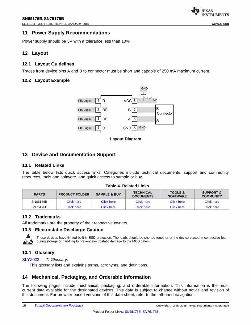
12 Layout
12.1 Layout GuidelinesTraces from device pins A and B to connector must be short and capable of 250 mA maximum current.
12.2 Layout Example
Layout Diagram
13 Device and Documentation Support
13.1 Related LinksThe table below lists quick access links. Categories include technical documents, support and communityresources, tools and software, and quick access to sample or buy.
Table 4. Related LinksTECHNICAL TOOLS & SUPPORT &PARTS PRODUCT FOLDER SAMPLE & BUY DOCUMENTS SOFTWARE COMMUNITY
SN65176B Click here Click here Click here Click here Click hereSN75176B Click here Click here Click here Click here Click here
13.2 TrademarksAll trademarks are the property of their respective owners.
13.3 Electrostatic Discharge CautionThese devices have limited built-in ESD protection. The leads should be shorted together or the device placed in conductive foamduring storage or handling to prevent electrostatic damage to the MOS gates.
13.4 GlossarySLYZ022 — TI Glossary.
This glossary lists and explains terms, acronyms, and definitions.
14 Mechanical, Packaging, and Orderable InformationThe following pages include mechanical, packaging, and orderable information. This information is the mostcurrent data available for the designated devices. This data is subject to change without notice and revision ofthis document. For browser-based versions of this data sheet, refer to the left-hand navigation.
16 Submit Documentation Feedback Copyright © 1985–2015, Texas Instruments Incorporated
Product Folder Links: SN65176B SN75176B

PACKAGE OPTION ADDENDUM
www.ti.com 15-Jun-2016
Addendum-Page 1
PACKAGING INFORMATION
Orderable Device Status(1)
Package Type PackageDrawing
Pins PackageQty
Eco Plan(2)
Lead/Ball Finish(6)
MSL Peak Temp(3)
Op Temp (°C) Device Marking(4/5)
Samples
SN65176BD ACTIVE SOIC D 8 75 Green (RoHS& no Sb/Br)
CU NIPDAU Level-1-260C-UNLIM -40 to 105 65176B
SN65176BDG4 ACTIVE SOIC D 8 75 Green (RoHS& no Sb/Br)
CU NIPDAU Level-1-260C-UNLIM -40 to 105 65176B
SN65176BDR ACTIVE SOIC D 8 2500 Green (RoHS& no Sb/Br)
CU NIPDAU Level-1-260C-UNLIM -40 to 105 65176B
SN65176BDRE4 ACTIVE SOIC D 8 2500 Green (RoHS& no Sb/Br)
CU NIPDAU Level-1-260C-UNLIM -40 to 105 65176B
SN65176BDRG4 ACTIVE SOIC D 8 2500 Green (RoHS& no Sb/Br)
CU NIPDAU Level-1-260C-UNLIM -40 to 105 65176B
SN65176BP ACTIVE PDIP P 8 50 Pb-Free(RoHS)
CU NIPDAU N / A for Pkg Type -40 to 105 SN65176BP
SN75176BD ACTIVE SOIC D 8 75 Green (RoHS& no Sb/Br)
CU NIPDAU Level-1-260C-UNLIM 0 to 70 75176B
SN75176BDE4 ACTIVE SOIC D 8 75 Green (RoHS& no Sb/Br)
CU NIPDAU Level-1-260C-UNLIM 0 to 70 75176B
SN75176BDG4 ACTIVE SOIC D 8 75 Green (RoHS& no Sb/Br)
CU NIPDAU Level-1-260C-UNLIM 0 to 70 75176B
SN75176BDR ACTIVE SOIC D 8 2500 Green (RoHS& no Sb/Br)
CU NIPDAU Level-1-260C-UNLIM 0 to 70 75176B
SN75176BDRE4 ACTIVE SOIC D 8 2500 Green (RoHS& no Sb/Br)
CU NIPDAU Level-1-260C-UNLIM 0 to 70 75176B
SN75176BDRG4 ACTIVE SOIC D 8 2500 Green (RoHS& no Sb/Br)
CU NIPDAU Level-1-260C-UNLIM 0 to 70 75176B
SN75176BP ACTIVE PDIP P 8 50 Pb-Free(RoHS)
CU NIPDAU N / A for Pkg Type 0 to 70 SN75176BP
SN75176BPE4 ACTIVE PDIP P 8 50 Pb-Free(RoHS)
CU NIPDAU N / A for Pkg Type 0 to 70 SN75176BP
SN75176BPSR ACTIVE SO PS 8 2000 Green (RoHS& no Sb/Br)
CU NIPDAU Level-1-260C-UNLIM 0 to 70 A176B
SN75176BPSRG4 ACTIVE SO PS 8 2000 Green (RoHS& no Sb/Br)
CU NIPDAU Level-1-260C-UNLIM 0 to 70 A176B
(1) The marketing status values are defined as follows:ACTIVE: Product device recommended for new designs.

PACKAGE OPTION ADDENDUM
www.ti.com 15-Jun-2016
Addendum-Page 2
LIFEBUY: TI has announced that the device will be discontinued, and a lifetime-buy period is in effect.NRND: Not recommended for new designs. Device is in production to support existing customers, but TI does not recommend using this part in a new design.PREVIEW: Device has been announced but is not in production. Samples may or may not be available.OBSOLETE: TI has discontinued the production of the device.
(2) Eco Plan - The planned eco-friendly classification: Pb-Free (RoHS), Pb-Free (RoHS Exempt), or Green (RoHS & no Sb/Br) - please check http://www.ti.com/productcontent for the latest availabilityinformation and additional product content details.TBD: The Pb-Free/Green conversion plan has not been defined.Pb-Free (RoHS): TI's terms "Lead-Free" or "Pb-Free" mean semiconductor products that are compatible with the current RoHS requirements for all 6 substances, including the requirement thatlead not exceed 0.1% by weight in homogeneous materials. Where designed to be soldered at high temperatures, TI Pb-Free products are suitable for use in specified lead-free processes.Pb-Free (RoHS Exempt): This component has a RoHS exemption for either 1) lead-based flip-chip solder bumps used between the die and package, or 2) lead-based die adhesive used betweenthe die and leadframe. The component is otherwise considered Pb-Free (RoHS compatible) as defined above.Green (RoHS & no Sb/Br): TI defines "Green" to mean Pb-Free (RoHS compatible), and free of Bromine (Br) and Antimony (Sb) based flame retardants (Br or Sb do not exceed 0.1% by weightin homogeneous material)
(3) MSL, Peak Temp. - The Moisture Sensitivity Level rating according to the JEDEC industry standard classifications, and peak solder temperature.
(4) There may be additional marking, which relates to the logo, the lot trace code information, or the environmental category on the device.
(5) Multiple Device Markings will be inside parentheses. Only one Device Marking contained in parentheses and separated by a "~" will appear on a device. If a line is indented then it is a continuationof the previous line and the two combined represent the entire Device Marking for that device.
(6) Lead/Ball Finish - Orderable Devices may have multiple material finish options. Finish options are separated by a vertical ruled line. Lead/Ball Finish values may wrap to two lines if the finishvalue exceeds the maximum column width.
Important Information and Disclaimer:The information provided on this page represents TI's knowledge and belief as of the date that it is provided. TI bases its knowledge and belief on informationprovided by third parties, and makes no representation or warranty as to the accuracy of such information. Efforts are underway to better integrate information from third parties. TI has taken andcontinues to take reasonable steps to provide representative and accurate information but may not have conducted destructive testing or chemical analysis on incoming materials and chemicals.TI and TI suppliers consider certain information to be proprietary, and thus CAS numbers and other limited information may not be available for release.
In no event shall TI's liability arising out of such information exceed the total purchase price of the TI part(s) at issue in this document sold by TI to Customer on an annual basis.

TAPE AND REEL INFORMATION
*All dimensions are nominal
Device PackageType
PackageDrawing
Pins SPQ ReelDiameter
(mm)
ReelWidth
W1 (mm)
A0(mm)
B0(mm)
K0(mm)
P1(mm)
W(mm)
Pin1Quadrant
SN65176BDR SOIC D 8 2500 330.0 12.4 6.4 5.2 2.1 8.0 12.0 Q1
SN65176BDRG4 SOIC D 8 2500 330.0 12.4 6.4 5.2 2.1 8.0 12.0 Q1
SN75176BDR SOIC D 8 2500 330.0 12.4 6.4 5.2 2.1 8.0 12.0 Q1
SN75176BDRG4 SOIC D 8 2500 330.0 12.4 6.4 5.2 2.1 8.0 12.0 Q1
SN75176BPSR SO PS 8 2000 330.0 16.4 8.2 6.6 2.5 12.0 16.0 Q1
PACKAGE MATERIALS INFORMATION
www.ti.com 13-Feb-2014
Pack Materials-Page 1

*All dimensions are nominal
Device Package Type Package Drawing Pins SPQ Length (mm) Width (mm) Height (mm)
SN65176BDR SOIC D 8 2500 340.5 338.1 20.6
SN65176BDRG4 SOIC D 8 2500 340.5 338.1 20.6
SN75176BDR SOIC D 8 2500 340.5 338.1 20.6
SN75176BDRG4 SOIC D 8 2500 340.5 338.1 20.6
SN75176BPSR SO PS 8 2000 367.0 367.0 38.0
PACKAGE MATERIALS INFORMATION
www.ti.com 13-Feb-2014
Pack Materials-Page 2


IMPORTANT NOTICE
Texas Instruments Incorporated and its subsidiaries (TI) reserve the right to make corrections, enhancements, improvements and otherchanges to its semiconductor products and services per JESD46, latest issue, and to discontinue any product or service per JESD48, latestissue. Buyers should obtain the latest relevant information before placing orders and should verify that such information is current andcomplete. All semiconductor products (also referred to herein as “components”) are sold subject to TI’s terms and conditions of salesupplied at the time of order acknowledgment.TI warrants performance of its components to the specifications applicable at the time of sale, in accordance with the warranty in TI’s termsand conditions of sale of semiconductor products. Testing and other quality control techniques are used to the extent TI deems necessaryto support this warranty. Except where mandated by applicable law, testing of all parameters of each component is not necessarilyperformed.TI assumes no liability for applications assistance or the design of Buyers’ products. Buyers are responsible for their products andapplications using TI components. To minimize the risks associated with Buyers’ products and applications, Buyers should provideadequate design and operating safeguards.TI does not warrant or represent that any license, either express or implied, is granted under any patent right, copyright, mask work right, orother intellectual property right relating to any combination, machine, or process in which TI components or services are used. Informationpublished by TI regarding third-party products or services does not constitute a license to use such products or services or a warranty orendorsement thereof. Use of such information may require a license from a third party under the patents or other intellectual property of thethird party, or a license from TI under the patents or other intellectual property of TI.Reproduction of significant portions of TI information in TI data books or data sheets is permissible only if reproduction is without alterationand is accompanied by all associated warranties, conditions, limitations, and notices. TI is not responsible or liable for such altereddocumentation. Information of third parties may be subject to additional restrictions.Resale of TI components or services with statements different from or beyond the parameters stated by TI for that component or servicevoids all express and any implied warranties for the associated TI component or service and is an unfair and deceptive business practice.TI is not responsible or liable for any such statements.Buyer acknowledges and agrees that it is solely responsible for compliance with all legal, regulatory and safety-related requirementsconcerning its products, and any use of TI components in its applications, notwithstanding any applications-related information or supportthat may be provided by TI. Buyer represents and agrees that it has all the necessary expertise to create and implement safeguards whichanticipate dangerous consequences of failures, monitor failures and their consequences, lessen the likelihood of failures that might causeharm and take appropriate remedial actions. Buyer will fully indemnify TI and its representatives against any damages arising out of the useof any TI components in safety-critical applications.In some cases, TI components may be promoted specifically to facilitate safety-related applications. With such components, TI’s goal is tohelp enable customers to design and create their own end-product solutions that meet applicable functional safety standards andrequirements. Nonetheless, such components are subject to these terms.No TI components are authorized for use in FDA Class III (or similar life-critical medical equipment) unless authorized officers of the partieshave executed a special agreement specifically governing such use.Only those TI components which TI has specifically designated as military grade or “enhanced plastic” are designed and intended for use inmilitary/aerospace applications or environments. Buyer acknowledges and agrees that any military or aerospace use of TI componentswhich have not been so designated is solely at the Buyer's risk, and that Buyer is solely responsible for compliance with all legal andregulatory requirements in connection with such use.TI has specifically designated certain components as meeting ISO/TS16949 requirements, mainly for automotive use. In any case of use ofnon-designated products, TI will not be responsible for any failure to meet ISO/TS16949.
Products ApplicationsAudio www.ti.com/audio Automotive and Transportation www.ti.com/automotiveAmplifiers amplifier.ti.com Communications and Telecom www.ti.com/communicationsData Converters dataconverter.ti.com Computers and Peripherals www.ti.com/computersDLP® Products www.dlp.com Consumer Electronics www.ti.com/consumer-appsDSP dsp.ti.com Energy and Lighting www.ti.com/energyClocks and Timers www.ti.com/clocks Industrial www.ti.com/industrialInterface interface.ti.com Medical www.ti.com/medicalLogic logic.ti.com Security www.ti.com/securityPower Mgmt power.ti.com Space, Avionics and Defense www.ti.com/space-avionics-defenseMicrocontrollers microcontroller.ti.com Video and Imaging www.ti.com/videoRFID www.ti-rfid.comOMAP Applications Processors www.ti.com/omap TI E2E Community e2e.ti.comWireless Connectivity www.ti.com/wirelessconnectivity
Mailing Address: Texas Instruments, Post Office Box 655303, Dallas, Texas 75265Copyright © 2016, Texas Instruments Incorporated