SNVS962A –DECEMBER 2013–REVISED NOVEMBER · PDF fileA4,B4 2 LED1 O High-Side...
40
1200 1400 1600 1800 2000 2200 2400 2600 2800 2.8 3 3.2 3.4 3.6 3.8 4 4.2 4.4 4.6 4.8 5 I IN (mA) V IN (V) TA = +25ºC TA = -40ºC TA = +85ºC C032 I LED = 1.5A, V LED = 3.7V IN OUT TEMP SW ENABLE TORCH TX SDA SCL GND 1 2H 10 2F 10 2F STROBE LED2 2.7V to 5.5V LED1 LM3646 Product Folder Sample & Buy Technical Documents Tools & Software Support & Community LM3646 SNVS962A – DECEMBER 2013 – REVISED NOVEMBER 2014 LM3646 1.5-A Synchronous Boost Converter With Dual High-Side Current Sources and I 2 C-Compatible Interface 1 Features 3 Description The LM3646 utilizes a 4-MHz fixed-frequency 1• High-Side Current Sources Allowing for Grounded synchronous boost converter to provide power to dual LED Cathode for Improved Thermal Management 1.5-A constant current LED sources. The high-side • > 85% Efficiency in Torch and Flash Modes current sources allow for grounded cathode LED • Small Solution Size < 20 mm 2 operation providing flash current up to 1.5 A total. An adaptive headroom regulation scheme ensures the • Accurate and Programmable Flash LED Current LED currents remain in regulation and maximizes from 24 mA to 1.5 A in 11.7-mA Steps efficiency. The combination of dual LED driving • Accurate and Programmable Torch LED Current capability, high LED current, small solution size and from 2.5 mA to 187 mA in 1.5-mA Steps high level of adjustability make the LM3646 perfect • Dual 1.5-A High-Side Current Sources for Dual for camera phone LED flash and torch applications. LED Drive The LM3646 is controlled through an I 2 C-compatible • Hardware Flash and Torch Enables interface. The main features of the LM3646 include: a hardware flash enable (STROBE) input for direct • Hardware Enable Pin triggering of the flash pulse, a hardware Torch enable • Soft-Start Operation for Battery Protection (TORCH) for movie mode or flashlight functions, a TX • LED Thermal Sensing and Current Scale-Back input which forces the flash pulse into a low-current torch mode allowing for synchronization to RF power • Synchronization Input for RF Power Amplifier amplifier events or other high-current conditions, an Pulse Events integrated comparator designed to monitor an NTC • VIN Flash Monitor Optimization thermistor and provide an interrupt to the LED • 1-MHz I²C-Compatible Interface current, and a programmable input voltage monitor • I²C-Programmable NTC Trip Point which monitors the battery voltage and can reduce the flash current during low battery conditions. A • 0.4-mm Pitch, 20-Bump DSBGA hardware enable (ENABLE) input provides a hardware shutdown during system software failures. 2 Applications The 4-MHz switching frequency, overvoltage Camera Phone LED Flash and Torch protection, and adjustable current limit allow for the use of tiny, low-profile inductors and (10-μF) ceramic capacitors. The device is available in a small 20- bump DSBGA package and operates over the –40°C to 85°C temperature range. Device Information (1) PART NUMBER PACKAGE BODY SIZE (NOM) LM3646 DSBGA (20) 2.015 mm x 1.615 mm (1) For all available packages, see the orderable addendum at the end of the datasheet. Typical Application Circuit System Performance 1 An IMPORTANT NOTICE at the end of this data sheet addresses availability, warranty, changes, use in safety-critical applications, intellectual property matters and other important disclaimers. PRODUCTION DATA.
Transcript of SNVS962A –DECEMBER 2013–REVISED NOVEMBER · PDF fileA4,B4 2 LED1 O High-Side...
1200
1400
1600
1800
2000
2200
2400
2600
2800
2.8 3 3.2 3.4 3.6 3.8 4 4.2 4.4 4.6 4.8 5
I IN (
mA
)
VIN (V)
TA = +25ºC
TA = -40ºC
TA = +85ºC
C032
ILED = 1.5A, VLED = 3.7V
IN OUT
TEMP
SW
ENABLE
TORCHTXSDASCL
GND
1 PH
10 PF 10 PF
STROBELED2
2.7V to 5.5V
LED1
LM3646
Product
Folder
Sample &Buy
Technical
Documents
Tools &
Software
Support &Community
LM3646SNVS962A –DECEMBER 2013–REVISED NOVEMBER 2014
LM3646 1.5-A Synchronous Boost Converter With Dual High-Side Current Sourcesand I2C-Compatible Interface
1 Features 3 DescriptionThe LM3646 utilizes a 4-MHz fixed-frequency
1• High-Side Current Sources Allowing for Groundedsynchronous boost converter to provide power to dualLED Cathode for Improved Thermal Management1.5-A constant current LED sources. The high-side
• > 85% Efficiency in Torch and Flash Modes current sources allow for grounded cathode LED• Small Solution Size < 20 mm2 operation providing flash current up to 1.5 A total. An
adaptive headroom regulation scheme ensures the• Accurate and Programmable Flash LED CurrentLED currents remain in regulation and maximizesfrom 24 mA to 1.5 A in 11.7-mA Stepsefficiency. The combination of dual LED driving
• Accurate and Programmable Torch LED Current capability, high LED current, small solution size andfrom 2.5 mA to 187 mA in 1.5-mA Steps high level of adjustability make the LM3646 perfect
• Dual 1.5-A High-Side Current Sources for Dual for camera phone LED flash and torch applications.LED Drive The LM3646 is controlled through an I2C-compatible
• Hardware Flash and Torch Enables interface. The main features of the LM3646 include: ahardware flash enable (STROBE) input for direct• Hardware Enable Pintriggering of the flash pulse, a hardware Torch enable• Soft-Start Operation for Battery Protection (TORCH) for movie mode or flashlight functions, a TX
• LED Thermal Sensing and Current Scale-Back input which forces the flash pulse into a low-currenttorch mode allowing for synchronization to RF power• Synchronization Input for RF Power Amplifieramplifier events or other high-current conditions, anPulse Eventsintegrated comparator designed to monitor an NTC• VIN Flash Monitor Optimizationthermistor and provide an interrupt to the LED
• 1-MHz I²C-Compatible Interface current, and a programmable input voltage monitor• I²C-Programmable NTC Trip Point which monitors the battery voltage and can reduce
the flash current during low battery conditions. A• 0.4-mm Pitch, 20-Bump DSBGAhardware enable (ENABLE) input provides ahardware shutdown during system software failures.2 ApplicationsThe 4-MHz switching frequency, overvoltageCamera Phone LED Flash and Torchprotection, and adjustable current limit allow for theuse of tiny, low-profile inductors and (10-μF) ceramiccapacitors. The device is available in a small 20-bump DSBGA package and operates over the –40°Cto 85°C temperature range.
Device Information(1)
PART NUMBER PACKAGE BODY SIZE (NOM)LM3646 DSBGA (20) 2.015 mm x 1.615 mm
(1) For all available packages, see the orderable addendum atthe end of the datasheet.
Typical Application Circuit System Performance
1
An IMPORTANT NOTICE at the end of this data sheet addresses availability, warranty, changes, use in safety-critical applications,intellectual property matters and other important disclaimers. PRODUCTION DATA.

LM3646SNVS962A –DECEMBER 2013–REVISED NOVEMBER 2014 www.ti.com
Table of Contents7.4 Device Functional Modes........................................ 141 Features .................................................................. 17.5 Programming........................................................... 172 Applications ........................................................... 17.6 Register Map........................................................... 193 Description ............................................................. 1
8 Application and Implementation ........................ 244 Revision History..................................................... 28.1 Application Information............................................ 245 Pin Configuration and Functions ......................... 38.2 Typical Application .................................................. 246 Specifications......................................................... 4
9 Power Supply Recommendations ...................... 326.1 Absolute Maximum Ratings ...................................... 410 Layout................................................................... 326.2 Handling Ratings....................................................... 4
10.1 Layout Guidelines ................................................. 326.3 Recommended Operating Conditions ...................... 410.2 Layout Example .................................................... 336.4 Thermal Information .................................................. 4
11 Device and Documentation Support ................. 346.5 Electrical Characteristics........................................... 511.1 Device Support...................................................... 346.6 Timing Requirements ................................................ 611.2 Documentation Support ........................................ 346.7 Typical Characteristics .............................................. 711.3 Trademarks ........................................................... 347 Detailed Description ............................................ 1211.4 Electrostatic Discharge Caution............................ 347.1 Overview ................................................................. 1211.5 Glossary ................................................................ 347.2 Functional Block Diagram ....................................... 13
12 Mechanical, Packaging, and Orderable7.3 Feature Description................................................. 13Information ........................................................... 34
4 Revision History
Changes from Original (December 2013) to Revision A Page
• Added Device Information and Handling Rating tables, Feature Description, Device Functional Modes, Applicationand Implementation, Power Supply Recommendations, Layout, Device and Documentation Support, andMechanical, Packaging, and Orderable Information sections; moved some curves to Application Curves section .............. 1
• Deleted "TX interrupt" .......................................................................................................................................................... 12• Changed reference to "Max LED Control Register (0x05)" to "Enable Register (0x01)" .................................................... 14• Added Control Truth table ................................................................................................................................................... 17
2 Submit Documentation Feedback Copyright © 2013–2014, Texas Instruments Incorporated
Product Folder Links: LM3646

Top View
A B C D E
Bottom View
E D C B A
1
2
3
4
1
2
3
4
LM3646www.ti.com SNVS962A –DECEMBER 2013–REVISED NOVEMBER 2014
5 Pin Configuration and Functions
DSBGA Package20 Pins
Pin FunctionsPIN
TYPE DESCRIPTIONNUMBER COUNT NAME
A1, B1 2 GND - Ground.A2, B2 2 SW O Drain Connection for Internal NMOS and Synchronous PMOS Switches.
A3, B3, C3 3 OUT O Step-Up DC/DC Converter Output. Connect a 10-µF ceramic capacitor between this pin andGND.
A4,B4 2 LED1 O High-Side Current Source Output for Flash LED. Both bumps must be connected for properoperation.
C1 1 AGND - Analog Ground.C2 1 TORCH I Active High Hardware Torch Enable. Drive TORCH high to turn on Torch/Movie Mode. Used
for External PWM mode. Has an internal pull-down resistor of 200 kΩ between TORCH andGND.
C4, D4 2 LED2 O High-Side Current Source Output for Flash LED. Both bumps must be connected for properoperation.
D1 1 IN I Input Voltage Connection. Connect IN to the input supply, and bypass to GND with a 10-µF orlarger ceramic capacitor.
D2 1 SCL I Serial Clock Input.D3 1 ENABLE I Active High Enable Pin. High = Standby, Low = Shutdown/Reset. Has an internal pull-down
resistor of 200 kΩ between ENABLE and GND.E1 1 TEMP O Threshold Detector for LED Temperature Sensing and Current Scale Back.E2 1 SDA I/O Serial Data Input/Output.E3 1 STROBE I Active High Hardware Flash Enable. Drive STROBE high to turn on Flash LEDs. STROBE
overrides TORCH. Has an internal pull-down resistor of 200 kΩ between STROBE and GND.E4 1 TX I Configurable Dual Polarity Power Amplifier Synchronization Input. Has an internal pull-down
resistor of 200 kΩ between TX and GND.
Copyright © 2013–2014, Texas Instruments Incorporated Submit Documentation Feedback 3
Product Folder Links: LM3646

LM3646SNVS962A –DECEMBER 2013–REVISED NOVEMBER 2014 www.ti.com
6 Specifications
6.1 Absolute Maximum Ratingsover operating free-air temperature range (unless otherwise noted) (1) (2)
MIN MAX UNIT−0.3 the lesser of VSCL, SDA, ENABLE, STROBE, TX, TORCH, LED1, LED2, TEMP (VIN+0.3) w/ 6 max
IN, SW, OUT −0.3 6 VInternallyContinuous power dissipation (3)Limited
Junction temperature (TJ-MAX) 150 °CMaximum lead temperature (soldering) See (4)
(1) Stresses beyond those listed under Absolute Maximum Ratings may cause permanent damage to the device. These are stress ratingsonly, and functional operation of the device at these or any other conditions beyond those indicated under Recommended OperatingConditions is not implied. Exposure to absolute-maximum-rated conditions for extended periods may affect device reliability.
(2) All voltages are with respect to the potential at the GND pin.(3) Internal thermal shutdown circuitry protects the device from permanent damage. Thermal shutdown engages at TJ = 135°C (typ.).
Thermal shutdown is verified by design.(4) For detailed soldering specifications and information, please refer to Texas Instruments Application Note 1112: DSBGA Wafer Level
Chip Scale Package (SNVA009).
6.2 Handling RatingsMIN MAX UNIT
Tstg Storage temperature range –65 150 °CHuman body model (HBM), per ANSI/ESDA/JEDEC JS-001, all –2500 2500pins (1)
V(ESD) Electrostatic discharge VCharged device model (CDM), per JEDEC specification –1500 1500JESD22-C101, all pins (2)
(1) JEDEC document JEP155 states that 500-V HBM allows safe manufacturing with a standard ESD control process.(2) JEDEC document JEP157 states that 250-V CDM allows safe manufacturing with a standard ESD control process.
6.3 Recommended Operating Conditionsover operating free-air temperature range (unless otherwise noted) (1) (2)
MIN MAX UNITVIN 2.7 5.5 VJunction temperature (TJ) −40 125 °CAmbient temperature (TA) (3) −40 85 °C
(1) Stresses beyond those listed under Absolute Maximum Ratings may cause permanent damage to the device. These are stress ratingsonly, and functional operation of the device at these or any other conditions beyond those indicated under Recommended OperatingConditions is not implied. Exposure to absolute-maximum-rated conditions for extended periods may affect device reliability.
(2) All voltages are with respect to the potential at the GND pin.(3) In applications where high power dissipation and/or poor package thermal resistance is present, the maximum ambient temperature may
have to be derated. Maximum ambient temperature (TA-MAX) is dependent on the maximum operating junction temperature (TJ-MAX-OP= 125°C), the maximum power dissipation of the device in the application (PD-MAX), and the junction-to-ambient thermal resistance of thepart/package in the application (RθJA), as given by the following equation: TA-MAX = TJ-MAX-OP – (RθJA × PD-MAX).
6.4 Thermal InformationLM3646
THERMAL METRIC (1) YFQ UNIT20 PINS
RθJA Junction-to-ambient thermal resistance 53.4 °C/W
(1) For more information about traditional and new thermal metrics, see the IC Package Thermal Metrics application report, SPRA953.
4 Submit Documentation Feedback Copyright © 2013–2014, Texas Instruments Incorporated
Product Folder Links: LM3646

LM3646www.ti.com SNVS962A –DECEMBER 2013–REVISED NOVEMBER 2014
6.5 Electrical CharacteristicsTypical (TYP) limits apply for TA = 25°C. Minimum (MIN) and maximum (MAX) limits apply over the full operating ambienttemperature range (−40°C ≤ TA ≤ 85°C). Unless otherwise specified, VIN = 3.6 V. (1) (2)
PARAMETER TEST CONDITIONS MIN TYP MAX UNITCURRENT SOURCE SPECIFICATIONS
1.395 1.5 1.605 A1.5A Flash, VOUT = 4 V, LED1 or LED2Active (−7%) (7%)
ILED1/2 Current source accuracy84.06 93.4 102.74 mA93.4 mA Torch, VOUT = 3.6 V, LED1 or
LED2 Active (−10%) (10%)250 280 mVILED = 1.5A Flash (12%)VOUT - Current source regulationVLED1/2 150 172.5ILED = 93.4 mA Torch (15%)
STEP-UP DC/DC CONVERTER SPECIFICATIONSICL Switch current limit −15% 1 15% A
−10% 3.1 10%VOVP Output overvoltage protection trip ON threshold 4.85 5.0 5.15 V
point OFF threshold 4.65 4.8 4.95RPMOS RPMOS switch on-resistance IPMOS = 1A 85 mΩRNMOS NMOS switch on-resistance INMOS = 1A 65UVLO Undervoltage lockout threshold Falling VIN 2.74 2.8 2.85 VVNTC-Trip NTC comparator trip threshold −6% 600 6% mVINTC NTC Current −6% 50 6% µAVNTC-Open NTC open trip threshold 2.2 2.3 2.4 VVNTC-Short NTC short trip threshold 75 100 125 mVVIVFM Input voltage flash monitor trip −5% 2.9 5% V
thresholdfSW Switching frequency 2.8 V ≤ VIN ≤ 4.8 V 3.72 4 4.28 MHzISD Shutdown supply current Device disabled, EN = 0 V 0.1 1.3 µA
2.8 V ≤ VIN ≤ 4.8 VISB Standby supply current Device disabled, EN = 1.8 V 2.5 10 µA
2.8 V ≤ VIN ≤ 4.8 VENABLE, STROBE, TORCH, TX VOLTAGE SPECIFICATIONSVIL Input logic low 2.8 V ≤ VIN ≤ 4.2 V 0 0.4 VVIH Input logic high 1.2 VIN
I2C-COMPATIBLE INTERFACE SPECIFICATIONS (SCL, SDA)VIL Input logic low 2.8 V ≤ VIN ≤ 4.2 V 0 0.4 VVIH Input logic high 1.2 VIN
VOL Output logic low ILOAD = 1.5 mA 300 mVtSCL SCL clock period 1 µs
(1) All voltages are with respect to the potential at the GND pin.(2) Min and Max limits are 100% production tested at an ambient temperature (TA) of 25°C. Limits over the operating temperature range are
specified through correlation using Statistical Quality Control (SQC) methods.
Copyright © 2013–2014, Texas Instruments Incorporated Submit Documentation Feedback 5
Product Folder Links: LM3646

I2C Flash I2C Stop STROBEI2C Bus
ILED ILED
TORCH
ILED
I2C Controlled Flash Start and Stop Delay Times
Strobe Controlled Flash Start and Stop Delay Times
External Indicator Start and Stop Delay TimesUsing Torch Pin
ILED
Flash time-out
ta tb tc td
te tf
tg th
TX event ± Start and Stop Delay Times
TX
EDGE TRIG STROBE
LM3646SNVS962A –DECEMBER 2013–REVISED NOVEMBER 2014 www.ti.com
6.6 Timing RequirementsDELAY EXPLANATION TIME
ta Time for the LED current to start ramping up after an I2C Write command. 560 µstb Time for the LED current to start ramping down after an I2C Stop command. 120 µstc Time for the LED current to start ramping up after the STROBE pin is raised high. 560 µstd Time for the LED current to start ramping down after the STROBE pin is pulled low. 8 µste Time for the LED current to start ramping up after the TORCH pin is raised high. 560 µstf Time for the LED current to start ramping down after the TORCH pin is pulled low. 8 µstg Time for the LED current to start ramping down after the TX pin is pulled high. 3 µs
Time for the LED current to start ramping up after the TX pin is pulled low, provided the part has not timedth 2 µsout in flash mode.
Figure 1. Control Logic Delays
6 Submit Documentation Feedback Copyright © 2013–2014, Texas Instruments Incorporated
Product Folder Links: LM3646

180
182
184
186
188
190
192
194
196
198
200
2.8 3 3.2 3.4 3.6 3.8 4 4.2 4.4 4.6 4.8 5
I LE
D (
mA
)
VIN (V)
D1, +25ºCD1, -40ºCD1, +85ºCD2, +25ºCD2, -40ºCD2, +85ºC
C003
1
1.1
1.2
1.3
1.4
1.5
1.6
1.7
1.8
2.5 2.8 3.1 3.4 3.7 4 4.3 4.6 4.9 5.2 5.5
I CL
(A)
VIN (V)
TA = +25ºC
TA = -40ºC
TA = +85ºC
C009
ILED = 1.5A, VLED = 4.5V
720
730
740
750
760
770
780
2.8 3 3.2 3.4 3.6 3.8 4 4.2 4.4 4.6 4.8 5
I LE
D (
mA
)
VIN (V)
D1, +25ºCD1, -40ºCD1, +85ºCD2, +25ºCD2, -40ºCD2, +85ºC
C002
0
20
40
60
80
100
120
140
160
180
200
0 8 16 24 32 40 48 56 64 72 80 88 96 104112120128
I LE
D (
mA
)
LED1 Code (#)
D1, +25ºCD1, -40ºCD1, +85ºCD2, +25ºCD2, -40ºCD2, +85ºC
C005
0
200
400
600
800
1000
1200
1400
1600
0 8 16 24 32 40 48 56 64 72 80 88 96 104112120128
I LE
D (
mA
)
LED1 Code (#)
D1, +25ºCD1, -40ºCD1, +85ºCD2, +25ºCD2, -40ºCD2, +85ºC
C004
1450
1460
1470
1480
1490
1500
1510
1520
1530
1540
1550
2.8 3 3.2 3.4 3.6 3.8 4 4.2 4.4 4.6 4.8 5
I LE
D (
mA
)
VIN (V)
D1, +25ºCD1, -40ºCD1, +85ºCD2, +25ºCD2, -40ºCD2, +85ºC
C001
LM3646www.ti.com SNVS962A –DECEMBER 2013–REVISED NOVEMBER 2014
6.7 Typical CharacteristicsUnless otherwise specified: TA= 25°C; VIN = 3.6 V; VEN = VIN; CIN = 10 µF; COUT = 10 µF; L = 1 µH.
Figure 2. Flash LED Current vs. Brightness Code Figure 3. Flash LED Current Line Regulation, ILED = 1.5A
Figure 5. Torch LED Current vs. Brightness CodeFigure 4. Flash LED Current Line Regulation,ILED1 = ILED2 = 0.75A
Figure 6. Torch LED Current Line Regulation, Figure 7. Inductor Current vs. Input Voltage, CL= 1 AILED = 187.1 mA
Copyright © 2013–2014, Texas Instruments Incorporated Submit Documentation Feedback 7
Product Folder Links: LM3646

1.4
1.6
1.8
2
2.2
2.4
2.6
2.8
3
2.5 2.8 3.1 3.4 3.7 4 4.3 4.6 4.9 5.2 5.5
I CL
(A)
VIN (V)
TA = +25ºC
TA = -40ºC
TA = +85ºC
C014
ILED = 1.5A, VLED = 4.5V
1.4
1.6
1.8
2
2.2
2.4
2.6
2.8
3
3.2
3.4
2.5 2.8 3.1 3.4 3.7 4 4.3 4.6 4.9 5.2 5.5
I CL
(A)
VIN (V)
TA = +25ºC
TA = -40ºC
TA = +85ºC
C015
ILED = 1.5A, VLED = 4.5V
1.4
1.5
1.6
1.7
1.8
1.9
2
2.1
2.2
2.3
2.5 2.8 3.1 3.4 3.7 4 4.3 4.6 4.9 5.2 5.5
I CL
(A)
VIN (V)
TA = +25ºC
TA = -40ºC
TA = +85ºC
C012
ILED = 1.5A, VLED = 4.5V
1.4
1.6
1.8
2
2.2
2.4
2.6
2.5 2.8 3.1 3.4 3.7 4 4.3 4.6 4.9 5.2 5.5
I CL
(A)
VIN (V)
TA = +25ºC
TA = -40ºC
TA = +85ºC
C013
ILED = 1.5A, VLED = 4.5V
1.2
1.3
1.4
1.5
1.6
1.7
1.8
1.9
2
2.5 2.8 3.1 3.4 3.7 4 4.3 4.6 4.9 5.2 5.5
I CL
(A)
VIN (V)
TA = +25ºC
TA = -40ºC
TA = +85ºC
C010
ILED = 1.5A, VLED = 4.5V
1.4
1.5
1.6
1.7
1.8
1.9
2
2.5 2.8 3.1 3.4 3.7 4 4.3 4.6 4.9 5.2 5.5
I CL
(A)
VIN (V)
TA = +25ºC
TA = -40ºC
TA = +85ºC
C011
ILED = 1.5A, VLED = 4.5V
LM3646SNVS962A –DECEMBER 2013–REVISED NOVEMBER 2014 www.ti.com
Typical Characteristics (continued)Unless otherwise specified: TA= 25°C; VIN = 3.6 V; VEN = VIN; CIN = 10 µF; COUT = 10 µF; L = 1 µH.
Figure 8. Inductor Current vs. Input Voltage, CL = 1.3 A Figure 9. Inductor Current vs. Input Voltage, CL = 1.6 A
Figure 10. Inductor Current vs. Input Voltage, CL = 1.9 A Figure 11. Inductor Current vs. Input Voltage, CL = 2.2 A
Figure 12. Inductor Current vs. Input Voltage, CL = 2.5 A Figure 13. Inductor Current vs. Input Voltage, CL = 2.8 A
8 Submit Documentation Feedback Copyright © 2013–2014, Texas Instruments Incorporated
Product Folder Links: LM3646

0.22
0.23
0.24
0.25
0.26
0.27
0.28
0.29
0.3
2.8 3 3.2 3.4 3.6 3.8 4 4.2 4.4 4.6
VF
B (
V)
VIN (V)
TA = +25ºC
TA = -40ºC
TA = +85ºC
C029
ILED = 1.5A, VLED = 4V
0.0001
0.0010
0.0100
0.1000
1.0000
2.5 2.8 3.1 3.4 3.7 4 4.3 4.6 4.9 5.2 5.5
I SD (
µA
)
VIN (V)
TA = +25ºC
TA = -40ºC
TA = +85ºC
C020
400
600
800
1000
1200
1400
1600
2.5 2.8 3.1 3.4 3.7 4 4.3 4.6 4.9 5.2 5.5
I LE
D (
mA
)
VIN (V)
CL = 1.0ACL = 1.3ACL = 1.6ACL = 1.9ACL = 2.2ACL = 2.5ACL = 2.8ACL = 3.1A
C017
ILED = 1.5A, VLED = 4V 1200
1400
1600
1800
2000
2200
2400
2600
2800
3000
3200
3400
2.5 2.8 3.1 3.4 3.7 4 4.3 4.6 4.9 5.2 5.5
I IN (
mA
)
VIN (V)
TA = +25ºC
TA = -40ºC
TA = +85ºC
C018
ILED = 1.5A, ICL = 3.1A, VLED = 4V
1.4
1.6
1.8
2
2.2
2.4
2.6
2.8
3
3.2
3.4
3.6
2.5 2.8 3.1 3.4 3.7 4 4.3 4.6 4.9 5.2 5.5
I CL
(A)
VIN (V)
TA = +25ºC
TA = -40ºC
TA = +85ºC
C016
ILED = 1.5A, VLED = 4.5V
0.9
1.2
1.5
1.8
2.1
2.4
2.7
3
3.3
3.6
2.5 2.8 3.1 3.4 3.7 4 4.3 4.6 4.9 5.2 5.5
I CL
(A)
VIN (V)
CL = 1.0ACL = 1.3ACL = 1.6ACL = 1.9ACL = 2.2ACL = 2.5ACL = 2.8ACL = 3.1A
C008
ILED = 1.5A, VLED = 4.5V
LM3646www.ti.com SNVS962A –DECEMBER 2013–REVISED NOVEMBER 2014
Typical Characteristics (continued)Unless otherwise specified: TA= 25°C; VIN = 3.6 V; VEN = VIN; CIN = 10 µF; COUT = 10 µF; L = 1 µH.
Figure 15. Inductor Current Limit vs. Input VoltageFigure 14. Inductor Current vs. Input Voltage, CL = 3.1 A
Figure 17. Input Current vs. Input VoltageFigure 16. Flash LED Current vs. Input Voltage in CurrentLimit
Figure 18. Current Source Headroom vs. Input Voltage Figure 19. Shutdown Current vs. Input Voltage
Copyright © 2013–2014, Texas Instruments Incorporated Submit Documentation Feedback 9
Product Folder Links: LM3646

47.0
47.5
48.0
48.5
49.0
49.5
50.0
2.5 2.8 3.1 3.4 3.7 4 4.3 4.6 4.9 5.2 5.5
I NT
C (
µA
)
VIN (V)
TA = +25ºC
TA = -40ºC
TA = +85ºC
C024
VNTC = 1.0V
0.55
0.56
0.57
0.58
0.59
0.6
0.61
0.62
0.63
0.64
0.65
2.5 2.8 3.1 3.4 3.7 4 4.3 4.6 4.9 5.2 5.5
VN
TC (
V)
VIN (V)
TA = +25ºC
TA = -40ºC
TA = +85ºC
C026
450
500
550
600
650
700
750
800
850
900
2.5 2.8 3.1 3.4 3.7 4 4.3 4.6 4.9 5.2 5.5
I Q (
µA
)
VIN (V)
TA = +25ºC
TA = -40ºC
TA = +85ºC
C023
ILED = 0
3.8
3.85
3.9
3.95
4
4.05
4.1
4.15
4.2
4.25
4.3
2.7 2.9 3.1 3.3 3.5 3.7 3.9 4.1 4.3 4.5 4.7
f SW
(M
Hz)
VIN (V)
TA = +25ºC
TA = -40ºC
TA = +85ºC
C019
0
2
4
6
8
10
12
14
2.5 2.8 3.1 3.4 3.7 4 4.3 4.6 4.9 5.2 5.5
I SB (
µA
)
VIN (V)
TA = +25ºC
TA = -40ºC
TA = +85ºC
C021
0.4
0.6
0.8
1
1.2
1.4
1.6
1.8
2
2.5 2.8 3.1 3.4 3.7 4 4.3 4.6 4.9 5.2 5.5
I SB (
µA
)
VIN (V)
TA = +25ºC
TA = -40ºC
TA = +85ºC
C022
LM3646SNVS962A –DECEMBER 2013–REVISED NOVEMBER 2014 www.ti.com
Typical Characteristics (continued)Unless otherwise specified: TA= 25°C; VIN = 3.6 V; VEN = VIN; CIN = 10 µF; COUT = 10 µF; L = 1 µH.
Figure 20. Standby Current vs. Input Voltage, VEN = 1.8 V Figure 21. Standby Current vs. Input Voltage, VEN = VIN
Figure 22. Input Current vs. Input Voltage in Pass Mode Figure 23. Frequency vs. Input Voltage
Figure 24. NTC Bias Current vs. Input Voltage Figure 25. NTC Threshold vs. Input Voltage, VNTC = 0.6 V
10 Submit Documentation Feedback Copyright © 2013–2014, Texas Instruments Incorporated
Product Folder Links: LM3646

46
47
48
49
50
51
2.5 2.8 3.1 3.4 3.7 4 4.3 4.6 4.9 5.2 5.5
I NT
C (
µA
)
VIN (V)
VNTC = 0.5V
VNTC = 1.0V
VNTC = 1.5V
VNTC = 2.0V
C025
2.25
2.27
2.29
2.31
2.33
2.35
2.5 2.8 3.1 3.4 3.7 4 4.3 4.6 4.9 5.2 5.5
VN
TC (
V)
VIN (V)
TA = +25ºC
TA = -40ºC
TA = +85ºC
C027
LM3646www.ti.com SNVS962A –DECEMBER 2013–REVISED NOVEMBER 2014
Typical Characteristics (continued)Unless otherwise specified: TA= 25°C; VIN = 3.6 V; VEN = VIN; CIN = 10 µF; COUT = 10 µF; L = 1 µH.
Figure 26. NTC Bias Current vs. Input Voltage at Different Figure 27. NTC Open Threshold vs. Input VoltageVNTC
Copyright © 2013–2014, Texas Instruments Incorporated Submit Documentation Feedback 11
Product Folder Links: LM3646

LM3646SNVS962A –DECEMBER 2013–REVISED NOVEMBER 2014 www.ti.com
7 Detailed Description
7.1 OverviewThe LM3646 is a high-power white LED flash driver capable of delivering up to 1.5 A (total LED current) into twoparallel LEDs. The device incorporates a 4-MHz constant frequency, synchronous Current-Mode PWM boostconverter, and two high-side current sources to regulate the LED current over the 2.7 V to 5.5 V input voltagerange.
The LM3646 PWM converter switches and maintains at least VHR across the current sources (LED1 and LED2).This minimum headroom voltage ensures that the current source remains in regulation. If the input voltage isabove the LED voltage + current source headroom voltage, the device does not switch and turns the PFET oncontinuously (Pass Mode). In Pass Mode the difference between (VIN - ILED x RPMOS) and the voltage across theLED is dropped across the current sources.
The LM3646 has three logic inputs including a hardware Flash Enable (STROBE), a hardware Torch Enable(TORCH) used for external Torch Mode control, and a Flash Interrupt input (TX) designed to interrupt the flashpulse during high battery current conditions. All three logic inputs have internal 200 kΩ (typ.) pull-down resistorsto GND.
Additional features of the LM3646 include an internal comparator for LED thermal sensing via an external NTCthermistor and an input voltage monitor that can reduce the Flash current (during low VIN conditions).
Control of the LM3646 is done via an I2C-compatible interface. This includes adjustment of the Flash and Torchcurrent levels, current source selection, changing the Flash Timeout Duration, changing the switch current limit,and enabling the NTC block. Additionally, there are flag and status bits that indicate flash current time-out, LEDover-temperature condition, LED failure (open/short), device thermal shutdown and VIN undervoltage conditions.
12 Submit Documentation Feedback Copyright © 2013–2014, Texas Instruments Incorporated
Product Folder Links: LM3646

+-
VOVP
PWM Control
ThermalShutdown
+150oC
INVREF
I2C
Interface
+
-
+ -
ErrorAmplifier
SlopeCompensation
SDA
SCL
ControlLogic/
Registers
GND
OUT
LED1
TEMP
TXSTROBETORCHENABLE
SW
65 m:
85 m:
Over Voltage Comparator
+-
NTC VTRIP
INTC
ILED1
Soft-Start
+-
4 MHzOscillator
+-
UVLOInput Voltage Flash Monitor
OUT-VHR
ILED2
LED2FB
SELECT
Current Sense/Current Limit
LM3646www.ti.com SNVS962A –DECEMBER 2013–REVISED NOVEMBER 2014
7.2 Functional Block Diagram
7.3 Feature Description
7.3.1 Flash ModeIn Flash Mode, the LED current sources (LED1/2) provide 128 target current levels from 0 mA to 1500 mA. TheFlash currents are adjusted via bits[3:0] of the Max LED Current Control Register (0x05) and bits[6:0] of theLED1 Flash Current Control Register (0x06). Flash Mode is activated by the Enable Register (0x01), or by pullingthe STROBE pin HIGH. Once the Flash sequence is activated the current source (LED) will ramp up to theprogrammed Flash current by stepping through all current steps until the programmed current is reached.
While both LED1 and LED2 are capable of delivering 1.5A to the LED, the sum total of the LED current will notexceed the value stored in the Max LED Current Control Register. LED1 will receive the current value stored inthe LED1 Flash Current Control Register, and LED2 will receive the difference of the value stored in the MAXLED Current Control Register and LED1 Flash Current Control Register.
If LED1 and LED2 Active:LED1 = LED1 Flash Current Control ValueLED2 = MAX Flash Current Control Value - LED1 Flash Current Control ValueIf MAX Flash Current Control Value < LED1 Flash Current Control ValueLED1 = MAX Flash Current Control Value
Copyright © 2013–2014, Texas Instruments Incorporated Submit Documentation Feedback 13
Product Folder Links: LM3646

LM3646SNVS962A –DECEMBER 2013–REVISED NOVEMBER 2014 www.ti.com
Feature Description (continued)LED2 = Off
If the LED1 Current Control Value is set to a level that is higher than the MAX Flash LED Current Control Value,LED1 receives the MAX Flash LED Current Control value, and LED2 is disabled.
When the part is enabled in Flash Mode through the Enable Register or the STROBE pin, all mode bits in theEnable Register are cleared after completion of the flash event. Before the device can be enabled again, themode bits need to be set.
7.3.2 Torch ModeIn Torch Mode, the LED current sources (LED1/2) provide 128 target current levels from 0 mA to 187.5 mA. TheTorch currents are adjusted via bits[6:4] of the Max LED Current Control Register (0x05) and bits[6:0] of theLED1 Torch Current Control Register (0x07). Torch Mode is activated by the Enable Register (0x01), or bypulling the TORCH pin HIGH. Once the TORCH sequence is activated the current source (LED) will ramp up tothe programmed Torch current by stepping through all current steps until the programmed current is reached.
LED1 receives the current value stored in the LED1 Torch Current Control Register, and LED2 receives thedifference of the value stored in the MAX LED Current Control Register and LED1 Torch Current ControlRegister.
If LED1 and LED2 Active:LED1 = LED1 Torch Current Control ValueLED2 = MAX Torch Current Control Value - LED1 Torch Current Control ValueIf MAX Torch Current Control Value < LED1 Torch Current Control ValueLED1 = MAX Torch Current Control ValueLED2 = Off
If the LED1 Torch Current Control Value is set to a level that is higher than the MAX Torch LED Current ControlValue, LED1 receives the MAX Torch LED Current Control value, and LED2 is disabled. Torch Mode is notaffected by Flash Timeout.
7.4 Device Functional Modes
7.4.1 Start-Up (Enabling the Device)Turn on of the LM3646 Torch and Flash Modes can be done through the Enable Register (0x01). On start-up,when VOUT is less than VIN, the internal synchronous PFET turns on as a current source and delivers 200 mA(typ.) to the output capacitor. During this time the current source (LED) is off. When the voltage across the outputcapacitor reaches 2.2 V (typ.) the current source turns on. At turnon the current source steps through eachFLASH or TORCH level until the target LED current is reached. This gives the device a controlled turn-on andlimits inrush current from the VIN supply.
7.4.2 Pass ModeThe LM3646 starts up in Pass Mode and stays there until Boost Mode is needed to maintain regulation. In PassMode the boost converter does not switch and the synchronous PFET turns fully on bringing VOUT up to VIN -(ILED x RPMOS). In Pass Mode the inductor current is not limited by the peak current limit. In this situation theoutput current must be limited to 2A. If the voltage difference between VOUT and VLED falls below VHR, the deviceswitches to Boost Mode.
7.4.3 Power Amplifier Synchronization (TX)The TX pin is a Power Amplifier Synchronization input. This is designed to reduce the flash LED current and thuslimit the battery current during high battery current conditions such as PA transmit events. When the LM3646 isengaged in a Flash event and the TX pin is pulled high, the LED current is forced into Torch Mode at theprogrammed Torch current setting. If the TX pin is then pulled low before the Flash pulse terminates, the LEDcurrent will return to the previous Flash current level. At the end of the Flash time-out, whether the TX pin is highor low, the LED current will turn off. The TX input can be disabled by setting bit TX Pin Enable to a ‘0’ in theEnable Register (0x01).
14 Submit Documentation Feedback Copyright © 2013–2014, Texas Instruments Incorporated
Product Folder Links: LM3646

IVM-D
IVM-U
tfilter
VIN
ILED
t
0 mA
IFLASH
IVM-D
IVM-U
tfilter tfilter
VIN
ILED
t
0 mA
IFLASH
LM3646www.ti.com SNVS962A –DECEMBER 2013–REVISED NOVEMBER 2014
Device Functional Modes (continued)7.4.4 Input Voltage Flash Monitor (IVFM)The LM3646 has the ability to adjust the flash current based upon the voltage level present at the IN pin utilizingan Input Voltage Flash Monitor. The IVFM block has an adjustable threshold (IVM-D) ranging from 2.9 V to 3.2 Vin 100-mV steps as well as adjustable hysteresis. The IVFM threshold and hysteresis are controlled by bits[4:3]and bits[2:1] respectively, in the IVFM Mode Register (0x02). Flags Register1 (0x08) has the IVFM flag (bit[3])set when the input voltage crosses the IVFM value. The IVFM threshold sets the input voltage boundary thatforces the LM3646 to stop ramping the flash current during startup in Stop and Hold Mode, or to actively adjustthe LED current lower in Down Adjust Mode, or to continuously adjust the LED current up and down in Up &Down mode.
Stop and Hold Mode (Figure 28): Stops Current Ramp and Holds the level for the remaining flash if VIN crossesIVM-D Line. Sets IVFM Flag (bit[3] in Flags Register1) upon crossing IVM-D Line.
Down Mode (Figure 29): Adjusts current down if VIN crosses IVM-D Line and stops decreasing once VIN risesabove the IVM-D line + the IVFM hysteresis setting. The LM3646 will decrease the current throughout the flashpulse anytime the input voltage falls below the IVM-D line, not just once. The flash current will not increase againuntil the next flash. Sets IVFM Flag (bit[3] in Flags Register1) upon crossing IVM-D Line.
Up and Down Mode (Figure 30): Adjusts current down if VIN crosses IVM-D Line and adjusts current up if VINrises above the IVM-D line + the IVFM hystersis setting. In this mode, the current will continually adjust with therising and falling of the input voltage throughout the entire flash pulse. Sets IVFM Flag (bit[3] in Flags Register1)upon crossing IVM-D Line.
Figure 28. IVFM Stop and Hold Mode
Figure 29. IVFM Down Mode
Copyright © 2013–2014, Texas Instruments Incorporated Submit Documentation Feedback 15
Product Folder Links: LM3646

IVM-D
IVM-U
tfilter
VIN
ILED
t
0 mA
IFLASH
tfilter tfilter
LM3646SNVS962A –DECEMBER 2013–REVISED NOVEMBER 2014 www.ti.com
Device Functional Modes (continued)
Figure 30. IVFM Up and Down Mode
7.4.5 Fault/Protections
7.4.5.1 Fault OperationUpon entering a fault condition, the LM3646 sets the appropriate flag in the Flags Register1 (0x08) or FlagsRegister2 (0x09), and place the part into standby by clearing and locking the Torch Enable bit (bit[7] in LED1Torch Current Control Register (0x07)) and Mode Bits (M1, M0) in the Enable Register (0x01), until the FlagsRegister1 or Flags Register2 is read back via I2C.
7.4.5.2 Flash Time-OutThe Flash Time-Out period sets the amount of time that the Flash Current is being sourced from the currentsource (LED). The LM3646 has 8 timeout levels ranging 50 ms to 400 ms in 50 ms steps. The Flash Time-Outperiod is controlled by bits[2:0] in the Flash Timing Register (0x04). Flash Time-Out only applies to the FlashMode operation. The mode bits are cleared and bit[0] is set in the Flags Register1 (0x08) upon a Flash Timeout.
7.4.5.3 Overvoltage Protection (OVP)The output voltage is limited to typically 5 V (see VOVP Spec). In situations such as an open LED, the LM3646raises the output voltage in order to try to keep the LED current at its target value. When VOUT reaches 5 V (typ.)the overvoltage comparator trips and turns off the internal NFET. When VOUT falls below the “VOVP OffThreshold”, the LM3646 begins switching again. The mode bits are cleared, and the OVP flag is set (bit[7] inFlags Register1 (0x08)) when an OVP condition is present for 512 microseconds, preventing momentary OVPevents from forcing the part to shut down.
7.4.5.4 Current LimitThe LM3646 features 8 selectable inductor current limits ranging from 1 A to 3.1 A in 300-mA steps. The currentlimit is programmable through bits[7:5] of the Enable Register (0x01) of the I2C-compatible interface. When theinductor current limit is reached, the LM3646 terminates the charging phase of the switching cycle.
Since the current limit is sensed in the NMOS switch, there is no mechanism to limit the current when the deviceoperates in Pass Mode. In Boost Mode or Pass Mode if VOUT falls below 2.3 V, the part stops switching, and thePFET operates as a current source limiting the current to 200 mA. This prevents damage to the LM3646 andexcessive current draw from the battery during output short-circuit conditions. The mode bits are not clearedupon a Current Limit event, but the OCP flag (bit[4]) in Flags Register1 (0x08) is set.
16 Submit Documentation Feedback Copyright © 2013–2014, Texas Instruments Incorporated
Product Folder Links: LM3646

LM3646www.ti.com SNVS962A –DECEMBER 2013–REVISED NOVEMBER 2014
Device Functional Modes (continued)7.4.5.5 NTC Thermistor Input (TEMP)The TEMP pin serves as a threshold detector for negative temperature coefficient (NTC) thermistors. It interruptsthe LED current and sets the NTC TRIP flag bit[6] in Flags Register1 (0x08) when the voltage at TEMP goesbelow the programmed threshold. The NTC threshold voltage is adjustable from 200 mV to 900 mV in 100 mVsteps via the NTC and Torch Ramp Register (0x03). The NTC current is set to 50 µA. When an over-temperatureevent is detected, the LM3646 is forced into shutdown. The NTC detection circuitry can be enabled or disabledvia bit[4] of the Enable Register (0x01). If Enabled, the NTC block will turn on and off during the start and stop ofa Flash/Torch event. The mode bits are cleared upon an NTC event.
Additionally, the NTC input looks for an open NTC connection and a short NTC connection. If the NTC input fallsbelow 100 mV, the NTC short flag is set (bit[1] in Flags Register2 (0x09)), and the part is disabled. If the NTCinput rises above 2.3 V, the NTC Open flag is set (bit[0] in Flags Register2), and the part is disabled. These faultdetections can be individually disabled/enabled via the NTC Open Detect Enable bit in IVFM Mode Register(0x02) and the NTC Short Fault Enable bit in Flags Register2.
7.4.5.6 Undervoltage Lockout (UVLO)The LM3646 has an internal comparator that monitors the voltage at IN and forces the LM3646 into shutdown ifthe input voltage drops to 2.8 V. If the UVLO monitor threshold is tripped, the UVLO flag bit is set in FlagsRegister1 (0x08). If the input voltage rises above 2.8 V, the LM3646 is not available for operation until there is anI2C read command initiated for the Flags Register1. Upon a read, Flags Register1 is cleared, and normaloperation can resume if the input voltage is greater than 2.8 V. This feature can be disabled by writing a ‘0’ to theUVLO Enable bit in the IVFM Mode Register (0x02). The mode bits are cleared upon a UVLO event.
7.4.5.7 Thermal Shutdown (TSD)When the LM3646’s die temperature reaches 135°C the boost converter shuts down, and the NFET and PFETturn off, as does the current source (LED). When the thermal shutdown threshold is tripped, a '1' gets written tobit[5] of Flags Register1 (0x08) (Thermal Shutdown bit), and the LM3646 will go into standby. The LM3646 isallowed to restart only after Flags Register1 is read, clearing the fault flag. Upon restart, if the die temperature isstill above 135°C, the LM3646 resets the Fault flag and re-enters standby. The mode bits are cleared upon aTSD.
7.4.5.8 LED and/or VOUT Short FaultThe LED Fault flags (bit[2] or bit[3]) in Flags Register2 (0x09) read back a '1' if the part is active in Flash or TorchMode and either LED output experiences a short condition. The Output Short Fault flag (bit[1] in Flags Register1(0x08)) reads back a '1' if the part is active in Flash or Torch Mode and the boost output experiences a shortcondition. An LED short condition is determined if the voltage at LED goes below 500 mV (typ.); VOUT shortcondition occurs if the voltage at OUT goes below 2.1 V (typ.) while the device is in Torch or Flash Mode. Thereis a delay of 256 μs deglitch time before the LED flag is valid and 2.048 ms before the VOUT flag is valid. Thisdelay is the time between when the Flash or Torch current is triggered, and when the LED voltage and the outputvoltage are sampled. The LED and VOUT short flags can only be reset to '0' by removing power to the LM3646,or by reading back the Flags Register1 or Flags Register2. The mode bits are cleared upon an LED and/orVOUT short fault.
7.5 Programming
7.5.1 Control Truth Table
Table 1. Control Truth TableMODE1 MODE0 STROBE EN TORCH EN STROBE PIN TORCH PIN ACTION
0 X X 0 X X Standby0 X X 1 X pos edge Ext Torch1 1 1 X pos edge X Ext Flash1 0 X 0 X X Int Torch1 1 0 X X X Int Flash
Copyright © 2013–2014, Texas Instruments Incorporated Submit Documentation Feedback 17
Product Folder Links: LM3646

SDA
Start Condition Stop Condition
SCLS P
SCL
SDA
data change allowed
data valid
data change allowed
data valid
data change allowed
LM3646SNVS962A –DECEMBER 2013–REVISED NOVEMBER 2014 www.ti.com
7.5.2 I2C-Compatible Interface
7.5.2.1 Data ValidityThe data on SDA line must be stable during the HIGH period of the clock signal (SCL). In other words, state ofthe data line can only be changed when SCL is LOW.
Figure 31. Data Validity Diagram
A pull-up resistor between the controller's VIO line and SDA must be greater than [(VIO-VOL) / 3mA] to meet theVOL requirement on SDA. Using a larger pullup resistor results in lower switching current with slower edges, whileusing a smaller pullup results in higher switching currents with faster edges.
7.5.2.2 START and STOP ConditionsSTART and STOP conditions classify the beginning and the end of the I2C session. A START condition isdefined as the SDA signal transitioning from HIGH to LOW while SCL line is HIGH. A STOP condition is definedas the SDA transitioning from LOW to HIGH while SCL is HIGH. The I2C-compatible master always generatesSTART and STOP conditions. The I2C-compatible bus is considered to be busy after a START condition and freeafter a STOP condition. During data transmission, the I2C-compatible master can generate repeated STARTconditions. First START and repeated START conditions are equivalent, function-wise.
Figure 32. Start and Stop Conditions
7.5.2.3 Transferring DataEvery byte put on the SDA line must be eight bits long, with the most significant bit (MSB) transferred first. Eachbyte of data has to be followed by an acknowledge bit. The acknowledge related clock pulse is generated by themaster. The master releases the SDA line (HIGH) during the acknowledge clock pulse. The LM3646 pulls downthe SDA line during the 9th clock pulse, signifying an acknowledge. The LM3646 generates an acknowledgeafter each byte is received. There is no acknowledge created after data is read from the LM3646.
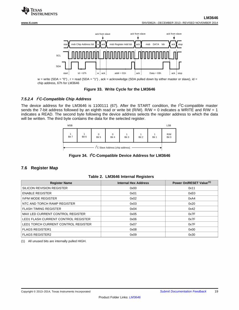
After the START condition, the I2C master sends a chip address. This address is seven bits long followed by aneighth bit which is a data direction bit (R/W). The LM3646 7-bit address is 0x67 (Figure 33). For the eighth bit, a'0' indicates a WRITE, and a '1' indicates a READ. The second byte selects the register to which the data will bewritten. The third byte contains data to write to the selected register.
18 Submit Documentation Feedback Copyright © 2013–2014, Texas Instruments Incorporated
Product Folder Links: LM3646
R/WBit 0
1Bit 1
1Bit 2
1Bit 3
0Bit 4
0Bit 5
1Bit 7
1Bit 6
MSB LSB
I2C Slave Address (chip address)
start msb Chip Address lsb w ack msb Register Add lsb ack msb DATA lsb ack stop
ack from slave ack from slave ack from slave
SCL
SDA
start Id = 67h w ack addr = 01h ack ackData = 03h stop
LM3646www.ti.com SNVS962A –DECEMBER 2013–REVISED NOVEMBER 2014
w = write (SDA = "0") , r = read (SDA = "1") , ack = acknowledge (SDA pulled down by either master or slave), id =chip address, 67h for LM3646
Figure 33. Write Cycle for the LM3646
7.5.2.4 I2C-Compatible Chip AddressThe device address for the LM3646 is 1100111 (67). After the START condition, the I2C-compatible mastersends the 7-bit address followed by an eighth read or write bit (R/W). R/W = 0 indicates a WRITE and R/W = 1indicates a READ. The second byte following the device address selects the register address to which the datawill be written. The third byte contains the data for the selected register.
Figure 34. I2C-Compatible Device Address for LM3646
7.6 Register Map
Table 2. LM3646 Internal RegistersRegister Name Internal Hex Address Power On/RESET Value (1)
SILICON REVISION REGISTER 0x00 0x11ENABLE REGISTER 0x01 0xE0IVFM MODE REGISTER 0x02 0xA4NTC AND TORCH RAMP REGISTER 0x03 0x20FLASH TIMING REGISTER 0x04 0x42MAX LED CURRENT CONTROL REGISTER 0x05 0x7FLED1 FLASH CURRENT CONTROL REGISTER 0x06 0x7FLED1 TORCH CURRENT CONTROL REGISTER 0x07 0x7FFLAGS REGISTER1 0x08 0x00FLAGS REGISTER2 0x09 0x30
(1) All unused bits are internally pulled HIGH.
Copyright © 2013–2014, Texas Instruments Incorporated Submit Documentation Feedback 19
Product Folder Links: LM3646

LM3646SNVS962A –DECEMBER 2013–REVISED NOVEMBER 2014 www.ti.com
7.6.1 Silicon Revision Register (0x00)
Bit 7 Bit 6 Bit 5 Bit 4 Bit 3 Bit 2 Bit 1 Bit 0RFU Chip ID Current Value = '010' Silicon Revision Current Value = '001'
7.6.2 Enable Register (0x01)
Bit 7 Bit 6 Bit 5 Bit 4 Bit 3 Bit 2 Bit 1 Bit 0Inductor Current Limit NTC Enable TX Pin Enable Soft-Start Enable LED Mode Bits: M1, M0
000 = 1.0A 0 = Disabled 0 = Disabled Enable 0 = Disabled 00 = Standby (default)(default) (default) (default)001 = 1.3A 01 = Standby
1 = Enabled 1 = Enabled 1 = Enabled010 = 1.6A 10 = Torch011 = 1.9A 11 = Flash100 = 2.2A101 = 2.5A110 = 2.8A
111 = 3.1A (default)
NTC Enable Enables or Disables the NTC detection block when the LM3646 is enabledTX Pin EN Enables the TX pin and TX current reduction functionSoft-Start EN Enables the Pass-Mode startup sequence
LED Mode Bits (M1, M0)00–Standby Off01–Standby Off10–Torch Sets Torch Mode. If Torch EN = 0, Torch will start after I²C-compatible command.11–Flash Sets Flash Mode. If Strobe EN = 0, Flash will start after I²C-compatible command.
7.6.3 IVFM Mode Register (0x02)
Bit 7 Bit 6 Bit 5 Bit 4 Bit 3 Bit 2 Bit 1 Bit 0UVLO IVFM Filter IVFM Enable IVFM Level Adjust Threshold IVFM Mode/Hysteresis NTC Open
Enable(2.8 V) Fault Enable0 = Disabled 0 = 4 µs 0 = Disabled 00 = 2.9V (default) 00 = Ramp and Hold 0 = Disabled1 = Enabled (default) 1 = Enabled 01 = 3.0V 01 = 0mV Hyst (default)
(default) (default)1 = 256 µs 10 = 3.1V 10 = 50 mV Hyst (default) 1 = Enabled11 = 3.2V 11 = 100 mV Hyst
7.6.4 NTC and Torch Ramp Register (0x03)
Bit 7 Bit 6 Bit 5 Bit 4 Bit 3 Bit 2 Bit 1 Bit 0Boost Mode NTC Trip Thresholds Torch Current Ramp Times
00 = Automatic (default) 000 = 200 mV 000 = Ramp Disabled (default)01 = Force Pass-Mode 001 = 300 mV 001 = 16 ms10 = Force Boost-Mode 010 = 400 mV 010 = 32 ms
11 = Automatic 011 = 500 mV 011 = 64 ms100 = 600 mV (default) 100 = 128 ms
101 = 700 mV 101 = 256 ms110 = 800 mV 110 = 512 ms111 = 900 mV 111 = 1024 ms
20 Submit Documentation Feedback Copyright © 2013–2014, Texas Instruments Incorporated
Product Folder Links: LM3646

VIN
VTRIPControlLogic
NTC Control Block
TEMPINTC
NTC +-
LM3646www.ti.com SNVS962A –DECEMBER 2013–REVISED NOVEMBER 2014
Figure 35. NTC Control Block
The TEMP node is connected to an NTC resistor as shown in Figure 35. A constant current source from theinput is connected to this node. Any change in the voltage because of a change in the resistance of the NTCresistor is compared to a set VTRIP. The trip thresholds are selected by Bits[5:3] of the NTC and Torch RampRegister.
7.6.5 Flash Timing Register (0x04)
Bit 7 Bit 6 Bit 5 Bit 4 Bit 3 Bit 2 Bit 1 Bit 0IVFM Modulation Strobe Usage Flash Ramp Time Flash Time-Out Time0 = Down Adjust 0 = Level 000 = 256 µs (default) 000 = 50 ms
(default) 1 = Edge 001 = 512 µs 001 = 100 ms1 = Up/Down (default) 010 = 1.024 ms 010 = 150 ms (default)
Adjust 011 = 2.048 ms 011 = 200 ms100 = 4.096 ms 100 = 250 ms101 = 8.192 ms 101 = 300 ms110 = 16.384 ms 110 = 350 ms111 = 32.768 ms 111 = 400 ms
7.6.6 Max LED Current Control Register (0x05)
Bit 7 Bit 6 Bit 5 Bit 4 Bit 3 Bit 2 Bit 1 Bit 0LED Short Fault Max Torch Current Max Flash Current
Enable0 = Down Adjust 000 = 23.04 mA 0000 = 93.35 mA
(default) 001 = 46.48 mA 0001 = 187.10 mA1 = Up/Down Adjust 010 = 69.91 mA 0010 = 280.85 mA
011 = 93.35 mA 0011 = 374.60 mA100 = 116.79 mA 0100 = 468.35 mA101 = 140.23 mA 0101 = 562.10 mA110 = 163.66 mA 0110 = 655.85 mA
111 = 187.10 mA (default) 0111 = 749.60 mA1000 = 843.35 mA1001 = 937.10 mA1010 = 1030.85 mA1011 = 1124.60 mA1100 = 1218.35 mA1101 = 1312.10 mA1110 = 1405.85 mA
1111 = 1499.60 mA (default)
If LED1 and LED2 Active:LED2 = MAX Current Control Value - LED1 Current Control ValueIf MAX Current Control Value < LED1 Current Control ValueLED1 = MAX Current Control ValueLED2 = Off
Copyright © 2013–2014, Texas Instruments Incorporated Submit Documentation Feedback 21
Product Folder Links: LM3646

LM3646SNVS962A –DECEMBER 2013–REVISED NOVEMBER 2014 www.ti.com
7.6.7 LED1 Flash Current Control Register (0x06)
Bit 7 Bit 6 Bit 5 Bit 4 Bit 3 Bit 2 Bit 1 Bit 0Strobe Pin Enable LED1 Flash Current Level
Bit0 = Disabled 0x00= 0 mA, LED1 Disabled, LED2 = Max Flash Current
(default) 0x01 = 23.04 mA1 = Enabled 0x02 = 34.76 mA
0x03 = 46.48 mA0x04 = 58.19 mA
. . .0x7D = 1476.16 mA0x7E = 1487.88 mA
0x7F = 1499.60 mA, LED2 Disabled (default)
7.6.8 LED1 Torch Current Control Register (0x07)
LED1 TORCH CURRENT CONTROL REGISTER (0x07)Bit 7 Bit 6 Bit 5 Bit 4 Bit 3 Bit 2 Bit 1 Bit 0
Torch Pin Enable LED1 Torch Current LevelBit
0 = Disabled 0x00= 0 mA, LED1 Disabled, LED2 = Max Torch Current(default) 0x01 = 2.53 mA
1 = Enabled 0x02 = 3.99 mA0x03 = 5.46 mA0x04 = 6.92 mA
. . .0x7D = 184.17 mA0x7E = 185.64 mA
0x7F = 187.10 mA, LED2 Disabled (default)
7.6.9 Flags Register1 (0x08)
Bit 7 Bit 6 Bit 5 Bit 4 Bit 3 Bit 2 Bit 1 Bit 0OVP NTC TRIP THERMAL OCP IVFM UVLO VOUT SHORT FLASH
SHUTDOWN FAULT TIMEOUT0 = Default 0 = Default 0 = Default 0 = Default 0 = Default0 = Default 0 = Default 0 = Default
OVP Fault Over-Voltage Protection tripped. Open Output capacitor or open LED.NTC Trip Fault NTC Threshold crossed.Thermal Shutdown Fault LM3646 Die temperature reached thermal shutdown value.Over-Current Protection Event Flag Inductor Current limit value was reached.IVFM Flag IVFM block adjusted LED current.UVLO Fault UVLO Threshold crossed.VOUT Short Fault VOUT Short detected.Time-Out Flag Flash Time-Out detected.
Note: Faults require an I2C read-back of the “Flags Register” to resume operation. Flags report an event occurred, but do notinhibit future functionality. A read-back of the Flags Register will only get updated again if the fault or flag is still present upon arestart.
7.6.10 Flags Register2 (0x09)
Bit 7 Bit 6 Bit 5 Bit 4 Bit 3 Bit 2 Bit 1 Bit 0RFU SOFTWARE Fault NTC Short LED2 Short LED1 Short NTC Short NTC Open Flag
Shutdown Fault Fault FlagRESET Bit Fault EnableEnable
0 = Normal 0 = Disabled 0 = Disabled 0 = Default 0 = Default 0 = Default 0 = DefaultOperation 1 = Enabled 1 = Enabled(Default) (default) (default)
1 = RESET
22 Submit Documentation Feedback Copyright © 2013–2014, Texas Instruments Incorporated
Product Folder Links: LM3646
LM3646www.ti.com SNVS962A –DECEMBER 2013–REVISED NOVEMBER 2014
Software Reset Bit Writing to this bit resets the LM3646 to the default power up conditions. This bit self-clears upon assertion.Fault Shutdown Enable When Enabled, faults will force the LM3646 to shutdown. When disabled, faults will not force the LM3646 to
shutdown. The LM3646 protection mechanisms will remain active until the part is manually disabled via the I2Cbus.
NTC Short Fault Enable When enabled, NTC Short faults will be detected and reported. When disabled, NTC Short faults will not bedetected or reported.
LED2 Short Fault Set to a '1' if LED2 is shorted.LED1 Short Fault Set to a '1' if LED1 is shorted.NTC Short Fault The NTC Short Flag is set if the NTC pin voltage crosses below 100 mV during operation.NTC Open Fault The NTC Open Flag is set if the NTC pin voltage crosses above 2.3V during operation.
Note: An I2C readback of the Flags Register2 will clear both the NTC Open and NTC Short Flags.
Copyright © 2013–2014, Texas Instruments Incorporated Submit Documentation Feedback 23
Product Folder Links: LM3646

VIN
ENABLE
LM3646
SDA
SCL
LED1
LED2
OUT
SW
TX
TORCH
TEMP
STROBE
L1
VBATT
2.7V ± 5.5V
C1
10 µF
1 µH
C2
10 µF
D1
µC/µP
GND
D2
LM3646SNVS962A –DECEMBER 2013–REVISED NOVEMBER 2014 www.ti.com
8 Application and Implementation
NOTEInformation in the following applications sections is not part of the TI componentspecification, and TI does not warrant its accuracy or completeness. TI’s customers areresponsible for determining suitability of components for their purposes. Customers shouldvalidate and test their design implementation to confirm system functionality.
8.1 Application InformationThe LM3646 can drive two flash LED at currents up to 1.5 A total. The 4-MHz DC/DC boost regulator allows forthe use of small value discrete external components.
8.2 Typical Application
Figure 36. Typical Application Circuit
24 Submit Documentation Feedback Copyright © 2013–2014, Texas Instruments Incorporated
Product Folder Links: LM3646

where IN INOUT
( )- VVxVL =I'
OUTSW VxLxfx2
I+xR=V LESRESR ''VxI OUTLED
VIN©§
¹·
Q =V'( )INOUTLED - VVxI
OUTOUTSW CxVxf
LM3646www.ti.com SNVS962A –DECEMBER 2013–REVISED NOVEMBER 2014
Typical Application (continued)8.2.1 Design RequirementsExample requirements based on default register values:
DESIGN PARAMETER EXAMPLE VALUEInput voltage range 2.5 V to 5.5 VBrightness control I2C Register
Inductor 1-µH, 3.1-A saturation CurrentLED configuration 2 Flash LEDs
Maximum flash brightness 1.5 AFlash brightness 1.5 A on LED1, LED2 Disabled
8.2.2 Detailed Design Procedure
8.2.2.1 Output Capacitor SelectionThe LM3646 is designed to operate with at least a 10-µF ceramic output capacitor. When the boost converter isrunning, the output capacitor supplies the load current during the boost converter's on-time. When the NMOSswitch turns off, the inductor energy is discharged through the internal PMOS switch, supplying power to the loadand restoring charge to the output capacitor. This causes a sag in the output voltage during the on-time and arise in the output voltage during the off-time. The output capacitor is therefore chosen to limit the output ripple toan acceptable level depending on load current and input/output voltage differentials and also to ensure theconverter remains stable.
For proper operation the output capacitor must be at least a 10-µF ceramic. Larger capacitors such as a 22-µF orcapacitors in parallel can be used if lower output voltage ripple is desired. To estimate the output voltage rippleconsidering the ripple due to capacitor discharge (ΔVQ) and the ripple due to the capacitor's ESR (ΔVESR), usethe following equations:
For continuous conduction mode, the output voltage ripple due to the capacitor discharge is:
(1)
The output voltage ripple due to the output capacitor's ESR is found by:
(2)
In ceramic capacitors the ESR is very low so a close approximation is to assume that 80% of the output voltageripple is due to capacitor discharge and 20% from ESR. Table 3 lists different manufacturers for various outputcapacitors and their case sizes suitable for use with the LM3646.
8.2.2.2 Input Capacitor SelectionChoosing the correct size and type of input capacitor helps minimize the voltage ripple caused by the switchingof the LM3646 device’s boost converter, and reduces noise on the boost converter's input pin that can feedthrough and disrupt internal analog signals. In the Figure 36 a 10-µF ceramic input capacitor works well. It isimportant to place the input capacitor as close as possible to the LM3646’s input (IN) pin. This reduces the seriesresistance and inductance that can inject noise into the device due to the input switching currents. Table 3 listsvarious input capacitors that are recommended for use with the LM3646.
Table 3. Recommended Input/Output Capacitors (X5R Dielectric)MANUFACTURER PART NUMBER VALUE CASE SIZE VOLTAGE RATINGTDK Corporation C1608JB0J106M 10 µF 0603 (1.6 mm × 0.8 mm × 0.8 mm) 6.3VTDK Corporation C2012JB1A106M 10 µF 0805 (2.0 mm × 1.25 mm × 1.25 mm) 10V
Copyright © 2013–2014, Texas Instruments Incorporated Submit Documentation Feedback 25
Product Folder Links: LM3646

ex( ) C25R=TR °2981
273+C°T1
E -¹·
©§
PEAKI LOADI=
Kx LI+' where L =I' IN xV ( )INOUT - VV
OUTSW VxLxfx2IN
OUT
V
V
LM3646SNVS962A –DECEMBER 2013–REVISED NOVEMBER 2014 www.ti.com
Table 3. Recommended Input/Output Capacitors (X5R Dielectric) (continued)MANUFACTURER PART NUMBER VALUE CASE SIZE VOLTAGE RATINGTDK Corporation C2012JB0J226M 22 µF 0805 (2.0 mm × 1.25 mm ×1.25 mm) 6.3V
Murata GRM21BR61A106KE19 10 µF 0805 (2.0 mm × 1.25 mm × 1.25 mm) 10VMurata GRM21BR60J226ME39L 22 µF 0805 (2.0 mm × 1.25 mm × 1.25 mm) 6.3V
8.2.2.3 Inductor SelectionThe LM3646 is designed to use a 1 µH or 2.2 µH inductor. Table 4 lists various inductors and theirmanufacturers that can work well with the LM3646. When the device is boosting (VOUT > VIN) the inductor willtypically be the largest area of efficiency loss in the circuit. Therefore, choosing an inductor with the lowestpossible series resistance is important. Additionally, the saturation rating of the inductor should be greater thanthe maximum operating peak current of the LM3646. This prevents excess efficiency loss that can occur withinductors that operate in saturation and prevents over-heating of the inductor and further efficiency loss. Forproper inductor operation and circuit performance ensure that the inductor saturation and the peak current limitsetting of the LM3646 is greater than IPEAK in the following calculation:
(3)
where ƒSW = 4 MHz, and efficiency can be found in the Typical Characteristics plots.
Table 4. Recommended InductorsMANUFACTURER VALUE PART NUMBER DIMENSIONS (L×W×H) ISAT RDC
TOKO 1 µH 1286AS-H-1R0N 2.0 mm × 1.6 mm × 1.2 mm 3.1A 68 mΩTOKO 1 µH 1285AS-H-1R0M 2.0 mm × 1.6 mm × 1.0 mm 2.7A 80 mΩTDK 1 µH TFM201610G-1R0M-T05 2.0 mm × 1.6 mm × 1.0 mm 2.9A 60 mΩ
8.2.2.4 NTC Thermistor SelectionThe TEMP pin is a comparator input for flash LED thermal sensing. NTC Mode is intended to monitor an externalthermistor which monitors LED temperature and prevents LED overheating. An internal comparator checks thevoltage on the TEMP pin against the trip point programmed in the NTC and Torch Ramp Register (0x03). Thethermistor is driven by an internally regulated current source, and the voltage on the TEMP pin is related to thesource current and the NTC resistance. NTC thermistors have a temperature to resistance relationship of:
(4)
where β is given in the thermistor datasheet and R25°C is the thermistor's value at 125°C.
Table 5. Application Circuit Component ListCOMPONENT MANUFACTURER VALUE PART NUMBER SIZE CURRENT/VOLTAGE
RATING (RESISTANCE)L TOKO 1 µH 1286AS-H-1R0N 2.0 mm x 1.6 mm x 1.2 mm ISAT = 3.1 A (68 mΩ)
COUT1,2 Murata 10 µF GRM188R60J106M 1.6 mm x 0.8 mm x 0.8 mm (0603) 6.3 VCIN1,2 Murata 10 µF GRM188R60J106M 1.6 mm x 0.8 mm x 0.8 mm (0603) 6.3 V
26 Submit Documentation Feedback Copyright © 2013–2014, Texas Instruments Incorporated
Product Folder Links: LM3646

t ± Time Base ± 100 µs/div
VOUT = 2 V/div
ILED = 1 A/div
IIN = 1 A/div
VLED = 2 V/div
t ± Time Base ± 100 µs/div
VOUT = 2 V/div
ILED = 1 A/div
IIN = 1 A/div
VLED = 2 V/div
50
60
70
80
90
100
100 300 500 700 900 1100 1300 1500
³LE
D (%
)
ILED (mA)
TA = +25ºC
TA = -40ºC
TA = +85ºC
C031
VIN = 3.7V
50
60
70
80
90
100
2.8 3 3.2 3.4 3.6 3.8 4 4.2 4.4 4.6 4.8 5
³LE
D (%
)
VIN (V)
TA = +25ºC
TA = -40ºC
TA = +85ºC
C007
ILED = 187.5mA, VLED = 3.2V
50
60
70
80
90
100
2.8 3 3.2 3.4 3.6 3.8 4 4.2 4.4 4.6 4.8 5
³LE
D (%
)
VIN (V)
TA = +25ºC
TA = -40ºC
TA = +85ºC
C006
ILED = 1.5A, VLED = 4V
50
60
70
80
90
100
2.8 3 3.2 3.4 3.6 3.8 4 4.2 4.4 4.6 4.8 5
³LE
D (%
)
VIN (V)
TA = +25ºC
TA = -40ºC
TA = +85ºC
C028
ILED = 750mA, VLED = 3.5V
LM3646www.ti.com SNVS962A –DECEMBER 2013–REVISED NOVEMBER 2014
8.2.3 Application CurvesUnless otherwise specified: TA= 25°C; VIN = 3.6 V; VEN = VIN; CIN = 10 µF; COUT = 10 µF; L = 1 µH.
Figure 37. Flash LED Efficiency vs. Input Voltage Figure 38. Flash LED Efficiency vs. Input Voltage
Figure 40. Torch LED Efficiency vs. Input VoltageFigure 39. Flash LED Efficiency vs. LED Current
Figure 42. Flash Ramp-DownFigure 41. Flash Ramp-Up
Copyright © 2013–2014, Texas Instruments Incorporated Submit Documentation Feedback 27
Product Folder Links: LM3646

t ± Time Base ± 1 ms/div
VOUT = 2 V/div
ILED = 1 A/div
IIN = 1 A/div
VLED = 2 V/div
IFLASH = 1.5A
ITORCH = 187mA
t ± Time Base ± 200 ns/div
VOUT = 200 mV/div
ILED = 10 mA/div
IIN = 20 mA/div
VLED = 200 mV/div
VIN = 3.3V
ILED = 750mA
t ± Time Base ± 200 ns/div
VOUT = 200 mV/div
ILED = 10 mA/div
IIN = 20 mA/div
VLED = 200 mV/div
VIN = 3.6V
ILED = 1.5A
t ± Time Base ± 200 ns/div
VOUT = 200 mV/div
ILED = 10 mA/div
IIN = 20 mA/div
VLED = 200 mV/div
VIN = 3.3V
ILED = 1.5A
t ± Time Base ± 40 µs/div
VOUT = 500 mV/div
ILED = 200 mA/div
VIN = 500 mV/div
t ± Time Base ± 40 µs/div
VOUT = 200 mV/div
ILED = 100 mA/div
VIN = 200 mV/div
LM3646SNVS962A –DECEMBER 2013–REVISED NOVEMBER 2014 www.ti.com
Unless otherwise specified: TA= 25°C; VIN = 3.6 V; VEN = VIN; CIN = 10 µF; COUT = 10 µF; L = 1 µH.
Figure 43. Line-step (200 mV) During Flash Figure 44. Line-step (400 mV) During Flash
Figure 46. LED Current RippleFigure 45. LED Current Ripple
Figure 47. LED Current Ripple Figure 48. TX-Mask Event, Default Settings
28 Submit Documentation Feedback Copyright © 2013–2014, Texas Instruments Incorporated
Product Folder Links: LM3646

t ± Time Base ± 100 µs/div
VIN = 200 mV/div
ILED = 500 mA/div
IIN = 1 A/div
tFILTER = ¼*tUVLO
tRAMP = 256µs
VHYST = 50mV
t ± Time Base ± 100 µs/div
VIN = 200 mV/div
ILED = 500 mA/div
IIN = 1 A/div
tFILTER = ¼*tUVLO
tRAMP = 256µs
VHYST = 50mV
t ± Time Base ± 40 µs/div
VTX = 5 V/div
ILED = 500 mA/div
IIN = 1 A/div
IFLASH = 1.5A
ITORCH = 100A
t ± Time Base ± 100 µs/div
VIN = 200 mV/div
ILED = 500 mA/div
IIN = 1 A/div
tFILTER = ¼*tUVLO
tRAMP = 256µs
t ± Time Base ± 1 µs/div
VTX = 5 V/div
ILED = 1 A/div
IIN = 1 A/div
IFLASH = 1.5A
ITORCH = 0A
t ± Time Base ± 1 µs/div
VTX = 5 V/div
ILED = 1 A/div
IIN = 1 A/div
IFLASH = 1.5A
ITORCH = 100A
LM3646www.ti.com SNVS962A –DECEMBER 2013–REVISED NOVEMBER 2014
Unless otherwise specified: TA= 25°C; VIN = 3.6 V; VEN = VIN; CIN = 10 µF; COUT = 10 µF; L = 1 µH.
Figure 49. TX Signal Low-to-High Transition Figure 50. TX Signal Low-to-High Transition
Figure 51. TX Signal High-to-Low Transition Figure 52. Input Voltage Flash Monitor, Stop & Hold Mode,Default settings
Figure 53. Input Voltage Flash Monitor, Down Mode, Figure 54. Input Voltage Flash Monitor, Up & Down Mode,Default Settings Default Settings
Copyright © 2013–2014, Texas Instruments Incorporated Submit Documentation Feedback 29
Product Folder Links: LM3646

t ± Time Base ± 400 µs/div
VIN = 200 mV/div
ILED = 1 A/div
IIN = 1 A/div
tFILTER = ¼*tUVLO
tRAMP = 256µs
VHYST = 50mV
VTX = 5 V/div
t ± Time Base ± 20 ms/div
VSTROBE = 2 V/div
ILED = 500 mA/div
t ± Time Base ± 200 µs/div
VIN = 200 mV/div
ILED = 500 mA/div
IIN = 1 A/div
tFILTER = 256µs
tRAMP = 256µs
VHYST = 50mV
t ± Time Base ± 100 µs/div
VIN = 200 mV/div
ILED = 500 mA/div
IIN = 1 A/div
tFILTER = ¼*tUVLO
tRAMP = 512µs
VHYST = 50mV
t ± Time Base ± 100 µs/div
VIN = 200 mV/div
ILED = 500 mA/div
IIN = 1 A/div
tFILTER = ¼*tUVLO
tRAMP = 256µs
VHYST = 0mV
t ± Time Base ± 100 µs/div
VIN = 200 mV/div
ILED = 500 mA/div
IIN = 1 A/div
tFILTER = ¼*tUVLO
tRAMP = 256µs
VHYST = 100mV
LM3646SNVS962A –DECEMBER 2013–REVISED NOVEMBER 2014 www.ti.com
Unless otherwise specified: TA= 25°C; VIN = 3.6 V; VEN = VIN; CIN = 10 µF; COUT = 10 µF; L = 1 µH.
Figure 55. Input Voltage Flash Monitor, Up & Down Mode, Figure 56. Input Voltage Flash Monitor, Up & Down Mode,
Figure 57. Input Voltage Flash Monitor, Up & Down Mode Figure 58. Input Voltage Flash Monitor, Up & Down Mode
Figure 59. Input Voltage Flash Monitor, Up & Down Mode Figure 60. Edge-Sensitive Strobewith TX Event
30 Submit Documentation Feedback Copyright © 2013–2014, Texas Instruments Incorporated
Product Folder Links: LM3646

t ± Time Base ± 20 ms/div
VSTROBE = 2 V/div
ILED = 500 mA/div
t ± Time Base ± 20 ms/div
VSTROBE = 2 V/div
ILED = 500 mA/div
LM3646www.ti.com SNVS962A –DECEMBER 2013–REVISED NOVEMBER 2014
Unless otherwise specified: TA= 25°C; VIN = 3.6 V; VEN = VIN; CIN = 10 µF; COUT = 10 µF; L = 1 µH.
Figure 62. Level-Sensitive Strobe with TimeoutFigure 61. Level-Sensitive Strobe without Timeout
Copyright © 2013–2014, Texas Instruments Incorporated Submit Documentation Feedback 31
Product Folder Links: LM3646

LM3646SNVS962A –DECEMBER 2013–REVISED NOVEMBER 2014 www.ti.com
9 Power Supply RecommendationsThe LM3646 is designed to operate from an input voltage supply range between 2.5 V and 5.5 V. This inputsupply must be well regulated and capable to supply the required input current. If the input supply is located farfrom the LM3646 additional bulk capacitance may be required in addition to the ceramic bypass capacitors.
10 Layout
10.1 Layout GuidelinesThe high switching frequency and large switching currents of the LM3646 make the choice of layout important.The following steps should be used as a reference to ensure the device is stable and maintains proper LEDcurrent regulation across its intended operating voltage and current range.1. Place CIN on the top layer (same layer as the LM3646) and as close to the device as possible. The input
capacitor conducts the driver currents during the low-side MOSFET turn-on and turn-off and can see currentspikes over 1 A in amplitude. Connecting the input capacitor through short, wide traces to both the IN andGND pins will reduce the inductive voltage spikes that occur during switching and which can corrupt the VINline.
2. Place COUT on the top layer (same layer as the LM3646) and as close as possible to the OUT and GND pins.The returns for both CIN and COUT should come together at one point, as close to the GND pin as possible.Connecting COUT through short, wide traces will reduce the series inductance on the OUT and GND pins thatcan corrupt the OUT and GND lines and cause excessive noise in the device and surrounding circuitry.
3. Connect the inductor on the top layer close to the SW pin. There should be a low-impedance connectionfrom the inductor to SW due to the large DC inductor current, and at the same time, the area occupied by theSW node should be small to reduce the capacitive coupling of the high dV/dt present at SW that can coupleinto nearby traces.
4. Avoid routing logic traces near the SW node to avoid any capacitively coupled voltages from SW onto anyhigh impedance logic lines such as TORCH, STROBE, ENABLE, TEMP, TX, SDA and SCL. A goodapproach is to insert an inner layer GND plane underneath the SW node and between any nearby routedtraces. This creates a shield from the electric field generated at SW.
5. Terminate the Flash LED cathodes directly to the GND pin of the LM3646. If possible, route the LED returnswith a dedicated path to keep the high amplitude LED currents out of the GND plane. For Flash LEDs thatare routed relatively far away from the LM3646, a good approach is to sandwich the forward and returncurrent paths over the top of each other on two layers. This will help in reducing the inductance of the LEDcurrent paths.
32 Submit Documentation Feedback Copyright © 2013–2014, Texas Instruments Incorporated
Product Folder Links: LM3646

GND SW
GND SW
SCL
SDA
EN
OUT
TORCH
TX
LED1
LED2
10 PF
10 PF
OUT
LED2
TEMP
LED1
TXSTROBESDA
INV
IAs
to G
ND
Plane
SW
OUT
OUT LED1
AGND
IN LED2
TEMP STROBE
1 P+
LM3646www.ti.com SNVS962A –DECEMBER 2013–REVISED NOVEMBER 2014
10.2 Layout Example
Figure 63. LM3646 Layout
Copyright © 2013–2014, Texas Instruments Incorporated Submit Documentation Feedback 33
Product Folder Links: LM3646

LM3646SNVS962A –DECEMBER 2013–REVISED NOVEMBER 2014 www.ti.com
11 Device and Documentation Support
11.1 Device Support
11.1.1 Third-Party Products DisclaimerTI'S PUBLICATION OF INFORMATION REGARDING THIRD-PARTY PRODUCTS OR SERVICES DOES NOTCONSTITUTE AN ENDORSEMENT REGARDING THE SUITABILITY OF SUCH PRODUCTS OR SERVICESOR A WARRANTY, REPRESENTATION OR ENDORSEMENT OF SUCH PRODUCTS OR SERVICES, EITHERALONE OR IN COMBINATION WITH ANY TI PRODUCT OR SERVICE.
11.2 Documentation Support
11.2.1 Related DocumentationFor related documentation, see the following:
Texas Instruments Application Note 1112: DSBGA Wafer Level Chip Scale Package (SNVA009).
11.3 TrademarksAll trademarks are the property of their respective owners.
11.4 Electrostatic Discharge CautionThis integrated circuit can be damaged by ESD. Texas Instruments recommends that all integrated circuits be handled withappropriate precautions. Failure to observe proper handling and installation procedures can cause damage.
ESD damage can range from subtle performance degradation to complete device failure. Precision integrated circuits may be moresusceptible to damage because very small parametric changes could cause the device not to meet its published specifications.
11.5 GlossarySLYZ022 — TI Glossary.
This glossary lists and explains terms, acronyms, and definitions.
12 Mechanical, Packaging, and Orderable InformationThe following pages include mechanical, packaging, and orderable information. This information is the mostcurrent data available for the designated devices. This data is subject to change without notice and revision ofthis document. For browser-based versions of this data sheet, refer to the left-hand navigation.
34 Submit Documentation Feedback Copyright © 2013–2014, Texas Instruments Incorporated
Product Folder Links: LM3646

PACKAGE OPTION ADDENDUM
www.ti.com 18-Aug-2014
Addendum-Page 1
PACKAGING INFORMATION
Orderable Device Status(1)
Package Type PackageDrawing
Pins PackageQty
Eco Plan(2)
Lead/Ball Finish(6)
MSL Peak Temp(3)
Op Temp (°C) Device Marking(4/5)
Samples
LM3646YFQR ACTIVE DSBGA YFQ 20 3000 Green (RoHS& no Sb/Br)
SNAGCU Level-1-260C-UNLIM -40 to 85 3646
(1) The marketing status values are defined as follows:ACTIVE: Product device recommended for new designs.LIFEBUY: TI has announced that the device will be discontinued, and a lifetime-buy period is in effect.NRND: Not recommended for new designs. Device is in production to support existing customers, but TI does not recommend using this part in a new design.PREVIEW: Device has been announced but is not in production. Samples may or may not be available.OBSOLETE: TI has discontinued the production of the device.
(2) Eco Plan - The planned eco-friendly classification: Pb-Free (RoHS), Pb-Free (RoHS Exempt), or Green (RoHS & no Sb/Br) - please check http://www.ti.com/productcontent for the latest availabilityinformation and additional product content details.TBD: The Pb-Free/Green conversion plan has not been defined.Pb-Free (RoHS): TI's terms "Lead-Free" or "Pb-Free" mean semiconductor products that are compatible with the current RoHS requirements for all 6 substances, including the requirement thatlead not exceed 0.1% by weight in homogeneous materials. Where designed to be soldered at high temperatures, TI Pb-Free products are suitable for use in specified lead-free processes.Pb-Free (RoHS Exempt): This component has a RoHS exemption for either 1) lead-based flip-chip solder bumps used between the die and package, or 2) lead-based die adhesive used betweenthe die and leadframe. The component is otherwise considered Pb-Free (RoHS compatible) as defined above.Green (RoHS & no Sb/Br): TI defines "Green" to mean Pb-Free (RoHS compatible), and free of Bromine (Br) and Antimony (Sb) based flame retardants (Br or Sb do not exceed 0.1% by weightin homogeneous material)
(3) MSL, Peak Temp. - The Moisture Sensitivity Level rating according to the JEDEC industry standard classifications, and peak solder temperature.
(4) There may be additional marking, which relates to the logo, the lot trace code information, or the environmental category on the device.
(5) Multiple Device Markings will be inside parentheses. Only one Device Marking contained in parentheses and separated by a "~" will appear on a device. If a line is indented then it is a continuationof the previous line and the two combined represent the entire Device Marking for that device.
(6) Lead/Ball Finish - Orderable Devices may have multiple material finish options. Finish options are separated by a vertical ruled line. Lead/Ball Finish values may wrap to two lines if the finishvalue exceeds the maximum column width.
Important Information and Disclaimer:The information provided on this page represents TI's knowledge and belief as of the date that it is provided. TI bases its knowledge and belief on informationprovided by third parties, and makes no representation or warranty as to the accuracy of such information. Efforts are underway to better integrate information from third parties. TI has taken andcontinues to take reasonable steps to provide representative and accurate information but may not have conducted destructive testing or chemical analysis on incoming materials and chemicals.TI and TI suppliers consider certain information to be proprietary, and thus CAS numbers and other limited information may not be available for release.
In no event shall TI's liability arising out of such information exceed the total purchase price of the TI part(s) at issue in this document sold by TI to Customer on an annual basis.

PACKAGE OPTION ADDENDUM
www.ti.com 18-Aug-2014
Addendum-Page 2

TAPE AND REEL INFORMATION
*All dimensions are nominal
Device PackageType
PackageDrawing
Pins SPQ ReelDiameter
(mm)
ReelWidth
W1 (mm)
A0(mm)
B0(mm)
K0(mm)
P1(mm)
W(mm)
Pin1Quadrant
LM3646YFQR DSBGA YFQ 20 3000 178.0 8.4 1.78 2.2 0.78 4.0 8.0 Q1
PACKAGE MATERIALS INFORMATION
www.ti.com 28-Nov-2014
Pack Materials-Page 1

*All dimensions are nominal
Device Package Type Package Drawing Pins SPQ Length (mm) Width (mm) Height (mm)
LM3646YFQR DSBGA YFQ 20 3000 220.0 220.0 35.0
PACKAGE MATERIALS INFORMATION
www.ti.com 28-Nov-2014
Pack Materials-Page 2

MECHANICAL DATA
YFQ0020xxx
www.ti.com
TMD20XXX (Rev D)
E
0.600±0.075
D
A. All linear dimensions are in millimeters. Dimensioning and tolerancing per ASME Y14.5M-1994.B. This drawing is subject to change without notice.
NOTES:
4215083/A 12/12
D: Max =
E: Max =
2.04 mm, Min =
1.64 mm, Min =
1.98 mm
1.58 mm

IMPORTANT NOTICE
Texas Instruments Incorporated (TI) reserves the right to make corrections, enhancements, improvements and other changes to itssemiconductor products and services per JESD46, latest issue, and to discontinue any product or service per JESD48, latest issue. Buyersshould obtain the latest relevant information before placing orders and should verify that such information is current and complete.TI’s published terms of sale for semiconductor products (http://www.ti.com/sc/docs/stdterms.htm) apply to the sale of packaged integratedcircuit products that TI has qualified and released to market. Additional terms may apply to the use or sale of other types of TI products andservices.Reproduction of significant portions of TI information in TI data sheets is permissible only if reproduction is without alteration and isaccompanied by all associated warranties, conditions, limitations, and notices. TI is not responsible or liable for such reproduceddocumentation. Information of third parties may be subject to additional restrictions. Resale of TI products or services with statementsdifferent from or beyond the parameters stated by TI for that product or service voids all express and any implied warranties for theassociated TI product or service and is an unfair and deceptive business practice. TI is not responsible or liable for any such statements.Buyers and others who are developing systems that incorporate TI products (collectively, “Designers”) understand and agree that Designersremain responsible for using their independent analysis, evaluation and judgment in designing their applications and that Designers havefull and exclusive responsibility to assure the safety of Designers' applications and compliance of their applications (and of all TI productsused in or for Designers’ applications) with all applicable regulations, laws and other applicable requirements. Designer represents that, withrespect to their applications, Designer has all the necessary expertise to create and implement safeguards that (1) anticipate dangerousconsequences of failures, (2) monitor failures and their consequences, and (3) lessen the likelihood of failures that might cause harm andtake appropriate actions. Designer agrees that prior to using or distributing any applications that include TI products, Designer willthoroughly test such applications and the functionality of such TI products as used in such applications.TI’s provision of technical, application or other design advice, quality characterization, reliability data or other services or information,including, but not limited to, reference designs and materials relating to evaluation modules, (collectively, “TI Resources”) are intended toassist designers who are developing applications that incorporate TI products; by downloading, accessing or using TI Resources in anyway, Designer (individually or, if Designer is acting on behalf of a company, Designer’s company) agrees to use any particular TI Resourcesolely for this purpose and subject to the terms of this Notice.TI’s provision of TI Resources does not expand or otherwise alter TI’s applicable published warranties or warranty disclaimers for TIproducts, and no additional obligations or liabilities arise from TI providing such TI Resources. TI reserves the right to make corrections,enhancements, improvements and other changes to its TI Resources. TI has not conducted any testing other than that specificallydescribed in the published documentation for a particular TI Resource.Designer is authorized to use, copy and modify any individual TI Resource only in connection with the development of applications thatinclude the TI product(s) identified in such TI Resource. NO OTHER LICENSE, EXPRESS OR IMPLIED, BY ESTOPPEL OR OTHERWISETO ANY OTHER TI INTELLECTUAL PROPERTY RIGHT, AND NO LICENSE TO ANY TECHNOLOGY OR INTELLECTUAL PROPERTYRIGHT OF TI OR ANY THIRD PARTY IS GRANTED HEREIN, including but not limited to any patent right, copyright, mask work right, orother intellectual property right relating to any combination, machine, or process in which TI products or services are used. Informationregarding or referencing third-party products or services does not constitute a license to use such products or services, or a warranty orendorsement thereof. Use of TI Resources may require a license from a third party under the patents or other intellectual property of thethird party, or a license from TI under the patents or other intellectual property of TI.TI RESOURCES ARE PROVIDED “AS IS” AND WITH ALL FAULTS. TI DISCLAIMS ALL OTHER WARRANTIES ORREPRESENTATIONS, EXPRESS OR IMPLIED, REGARDING RESOURCES OR USE THEREOF, INCLUDING BUT NOT LIMITED TOACCURACY OR COMPLETENESS, TITLE, ANY EPIDEMIC FAILURE WARRANTY AND ANY IMPLIED WARRANTIES OFMERCHANTABILITY, FITNESS FOR A PARTICULAR PURPOSE, AND NON-INFRINGEMENT OF ANY THIRD PARTY INTELLECTUALPROPERTY RIGHTS. TI SHALL NOT BE LIABLE FOR AND SHALL NOT DEFEND OR INDEMNIFY DESIGNER AGAINST ANY CLAIM,INCLUDING BUT NOT LIMITED TO ANY INFRINGEMENT CLAIM THAT RELATES TO OR IS BASED ON ANY COMBINATION OFPRODUCTS EVEN IF DESCRIBED IN TI RESOURCES OR OTHERWISE. IN NO EVENT SHALL TI BE LIABLE FOR ANY ACTUAL,DIRECT, SPECIAL, COLLATERAL, INDIRECT, PUNITIVE, INCIDENTAL, CONSEQUENTIAL OR EXEMPLARY DAMAGES INCONNECTION WITH OR ARISING OUT OF TI RESOURCES OR USE THEREOF, AND REGARDLESS OF WHETHER TI HAS BEENADVISED OF THE POSSIBILITY OF SUCH DAMAGES.Unless TI has explicitly designated an individual product as meeting the requirements of a particular industry standard (e.g., ISO/TS 16949and ISO 26262), TI is not responsible for any failure to meet such industry standard requirements.Where TI specifically promotes products as facilitating functional safety or as compliant with industry functional safety standards, suchproducts are intended to help enable customers to design and create their own applications that meet applicable functional safety standardsand requirements. Using products in an application does not by itself establish any safety features in the application. Designers mustensure compliance with safety-related requirements and standards applicable to their applications. Designer may not use any TI products inlife-critical medical equipment unless authorized officers of the parties have executed a special contract specifically governing such use.Life-critical medical equipment is medical equipment where failure of such equipment would cause serious bodily injury or death (e.g., lifesupport, pacemakers, defibrillators, heart pumps, neurostimulators, and implantables). Such equipment includes, without limitation, allmedical devices identified by the U.S. Food and Drug Administration as Class III devices and equivalent classifications outside the U.S.TI may expressly designate certain products as completing a particular qualification (e.g., Q100, Military Grade, or Enhanced Product).Designers agree that it has the necessary expertise to select the product with the appropriate qualification designation for their applicationsand that proper product selection is at Designers’ own risk. Designers are solely responsible for compliance with all legal and regulatoryrequirements in connection with such selection.Designer will fully indemnify TI and its representatives against any damages, costs, losses, and/or liabilities arising out of Designer’s non-compliance with the terms and provisions of this Notice.
Mailing Address: Texas Instruments, Post Office Box 655303, Dallas, Texas 75265Copyright © 2017, Texas Instruments Incorporated


