SNVS724C – JUNE 2011– REVISED MAY 2013 Compact Sequential ... · LM3435 SNVS724C – JUNE...
29
LM3435 www.ti.com SNVS724C – JUNE 2011 – REVISED MAY 2013 Compact Sequential Mode RGB LED Driver with I 2 C Control Interface Check for Samples: LM3435 1FEATURES KEY SPECIFICATIONS 23• Sequential RGB Driving Mode • Support up to 2A LED current • Low Component Count and Small Solution • Typical ±3% LED current accuracy Size • Integrated N-Channel main and P-Channel • Stable with Ceramic and Other Low ESR synchronous MOSFETs capacitors, No Loop Compensation Required • 3 Integrated N-Channel current regulating pass • Fast Transient Response switches • Programmable Converter Switching Frequency • LED Currents programmable via I 2 C bus up to 1 MHz independently • MCU Interface Ready With I 2 C Bus • Input voltage range: 2.7 – 5.5 V • Peak Current Limit Protection for the Switcher • Thermal shutdown • LED Fault Detection and Reporting via I 2 C Bus • Thermally enhanced WQFN package APPLICATIONS DESCRIPTION The LM3435, a Synchronously Rectified non-isolated • Li-ion Batteries/USB Powered RGB LED Driver Flyback Converter, features all required functions to • Pico/Pocket RGB LED Projector implement a highly efficient and cost effective RGB LED driver. Different from conventional Flyback TYPICAL APPLICATION converter, LEDs connect across the VOUT pin and the VIN pin through internal passing elements at corresponding LED pins. Thus, voltage across LEDs can be higher than, equal to or lower than the input supply voltage. Load current to LEDs is up to 2A with voltage across LEDs ranging from 2.0V to 4.5V. Integrated N- Channel main MOSFET, P-Channel synchronous MOSFET and three N-Channel current regulating pass switches allow low component count, thus reducing complexity and minimize board size. The LM3435 is designed to work exceptionally well with ceramic output capacitors with low output ripple voltage. Loop compensation is not required resulting in a fast load transient response. Non-overlapping RGB LEDs are driven sequentially through individual control. Output voltage hence can be optimized for different forward voltage of LEDs during the non- overlapping period. I 2 C™ interface eases the programming of the individual RGB LED current up to 1,024 levels per channel. The LM3435 is available in the thermally enhanced 40-pin WQFN package. 1 Please be aware that an important notice concerning availability, standard warranty, and use in critical applications of Texas Instruments semiconductor products and disclaimers thereto appears at the end of this data sheet. 2I 2 C is a trademark of NXP. 3All other trademarks are the property of their respective owners. PRODUCTION DATA information is current as of publication date. Copyright © 2011–2013, Texas Instruments Incorporated Products conform to specifications per the terms of the Texas Instruments standard warranty. Production processing does not necessarily include testing of all parameters.
Transcript of SNVS724C – JUNE 2011– REVISED MAY 2013 Compact Sequential ... · LM3435 SNVS724C – JUNE...
LM3435
www.ti.com SNVS724C –JUNE 2011–REVISED MAY 2013
Compact Sequential Mode RGB LED Driver with I2C Control InterfaceCheck for Samples: LM3435
1FEATURES KEY SPECIFICATIONS23• Sequential RGB Driving Mode • Support up to 2A LED current• Low Component Count and Small Solution • Typical ±3% LED current accuracy
Size • Integrated N-Channel main and P-Channel• Stable with Ceramic and Other Low ESR synchronous MOSFETs
capacitors, No Loop Compensation Required • 3 Integrated N-Channel current regulating pass• Fast Transient Response switches• Programmable Converter Switching Frequency • LED Currents programmable via I2C bus
up to 1 MHz independently• MCU Interface Ready With I2C Bus • Input voltage range: 2.7 – 5.5 V• Peak Current Limit Protection for the Switcher • Thermal shutdown• LED Fault Detection and Reporting via I2C Bus • Thermally enhanced WQFN package
APPLICATIONS DESCRIPTIONThe LM3435, a Synchronously Rectified non-isolated• Li-ion Batteries/USB Powered RGB LED DriverFlyback Converter, features all required functions to
• Pico/Pocket RGB LED Projector implement a highly efficient and cost effective RGBLED driver. Different from conventional Flyback
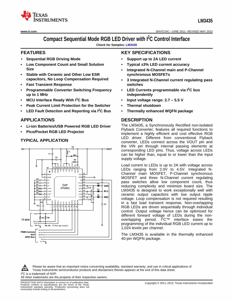
TYPICAL APPLICATION converter, LEDs connect across the VOUT pin andthe VIN pin through internal passing elements atcorresponding LED pins. Thus, voltage across LEDscan be higher than, equal to or lower than the inputsupply voltage.
Load current to LEDs is up to 2A with voltage acrossLEDs ranging from 2.0V to 4.5V. Integrated N-Channel main MOSFET, P-Channel synchronousMOSFET and three N-Channel current regulatingpass switches allow low component count, thusreducing complexity and minimize board size. TheLM3435 is designed to work exceptionally well withceramic output capacitors with low output ripplevoltage. Loop compensation is not required resultingin a fast load transient response. Non-overlappingRGB LEDs are driven sequentially through individualcontrol. Output voltage hence can be optimized fordifferent forward voltage of LEDs during the non-overlapping period. I2C™ interface eases theprogramming of the individual RGB LED current up to1,024 levels per channel.
The LM3435 is available in the thermally enhanced40-pin WQFN package.
1
Please be aware that an important notice concerning availability, standard warranty, and use in critical applications ofTexas Instruments semiconductor products and disclaimers thereto appears at the end of this data sheet.
2I2C is a trademark of NXP.3All other trademarks are the property of their respective owners.
PRODUCTION DATA information is current as of publication date. Copyright © 2011–2013, Texas Instruments IncorporatedProducts conform to specifications per the terms of the TexasInstruments standard warranty. Production processing does notnecessarily include testing of all parameters.
LM3435
SNVS724C –JUNE 2011–REVISED MAY 2013 www.ti.com
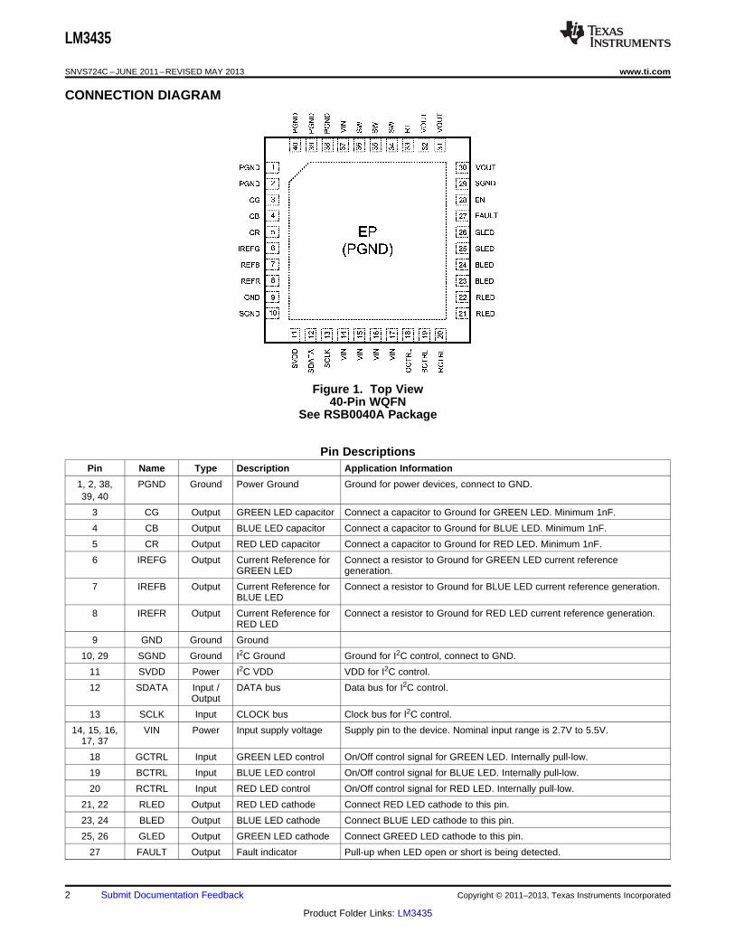
CONNECTION DIAGRAM
Figure 1. Top View40-Pin WQFN
See RSB0040A Package
Pin DescriptionsPin Name Type Description Application Information
1, 2, 38, PGND Ground Power Ground Ground for power devices, connect to GND.39, 40
3 CG Output GREEN LED capacitor Connect a capacitor to Ground for GREEN LED. Minimum 1nF.
4 CB Output BLUE LED capacitor Connect a capacitor to Ground for BLUE LED. Minimum 1nF.
5 CR Output RED LED capacitor Connect a capacitor to Ground for RED LED. Minimum 1nF.
6 IREFG Output Current Reference for Connect a resistor to Ground for GREEN LED current referenceGREEN LED generation.
7 IREFB Output Current Reference for Connect a resistor to Ground for BLUE LED current reference generation.BLUE LED
8 IREFR Output Current Reference for Connect a resistor to Ground for RED LED current reference generation.RED LED
9 GND Ground Ground
10, 29 SGND Ground I2C Ground Ground for I2C control, connect to GND.
11 SVDD Power I2C VDD VDD for I2C control.
12 SDATA Input / DATA bus Data bus for I2C control.Output
13 SCLK Input CLOCK bus Clock bus for I2C control.
14, 15, 16, VIN Power Input supply voltage Supply pin to the device. Nominal input range is 2.7V to 5.5V.17, 37
18 GCTRL Input GREEN LED control On/Off control signal for GREEN LED. Internally pull-low.
19 BCTRL Input BLUE LED control On/Off control signal for BLUE LED. Internally pull-low.
20 RCTRL Input RED LED control On/Off control signal for RED LED. Internally pull-low.
21, 22 RLED Output RED LED cathode Connect RED LED cathode to this pin.
23, 24 BLED Output BLUE LED cathode Connect BLUE LED cathode to this pin.
25, 26 GLED Output GREEN LED cathode Connect GREED LED cathode to this pin.
27 FAULT Output Fault indicator Pull-up when LED open or short is being detected.
2 Submit Documentation Feedback Copyright © 2011–2013, Texas Instruments Incorporated
Product Folder Links: LM3435
LM3435
www.ti.com SNVS724C –JUNE 2011–REVISED MAY 2013
Pin Descriptions (continued)
Pin Name Type Description Application Information
28 EN Input Enable pin Internally pull-up. Connect to a voltage lower than 0.2 x VIN to disable thedevice.
30, 31, 32 VOUT Input / Output voltage Connect anodes of LEDs to this pin.Output
33 RT Input ON-time control An external resistor connected from VOUT to this pin sets the mainMOSFET on-time, hence determine the switching frequency.
34, 35, 36 SW Output Switch node Internally connected to the drain of the main N-channel MOSFET and theP-channel synchronous MOSFET. Connect to the output inductor.
EP EP Ground Exposed Pad Thermal connection pad, connect to the GND pin.
These devices have limited built-in ESD protection. The leads should be shorted together or the device placed in conductive foamduring storage or handling to prevent electrostatic damage to the MOS gates.
ABSOLUTE MAXIMUM RATINGS (1)
VALUE / INPUTS
VIN to GND –0.3V to 6.0V
VOUT, RT to VIN –0.3V to 5.5V
RLED, GLED, BLED to VIN –0.3V to 5.5V
SW to GND –0.3V to 11.5V
SW to GND (Transient) –2V to 13V (<100 ns)
All other inputs to GND –0.3V to 6.0V
ESD Rating Human Body Model (2) ±1.5 kV
Storage Temperature –65°C to +150°C
Junction Temperature (TJ) –40°C to +125°C
(1) Absolute Maximum Ratings are limits which damage to the device may occur. Operating ratings are conditions under which operation ofthe device is intended to be functional. For specifications and test conditions, see the electrical characteristics.
(2) The human body model is a 100 pF capacitor discharged through a 1.5 kΩ resistor into each pin.
RECOMMENDED OPERATING CONDITIONS (1)
VALUE / INPUTS
Supply Voltage Range (VIN) 2.7V to 5.5V
Junction Temp. Range (TJ) –40°C to +125°C
Thermal Resistance (θJB) (2) 28°C/W
(1) Absolute Maximum Ratings are limits which damage to the device may occur. Operating ratings are conditions under which operation ofthe device is intended to be functional. For specifications and test conditions, see the electrical characteristics.
(2) θJB is junction-to-board thermal characteristic parameter. For packages with exposed pad, θJB is significantly dependent on PC boards.So, only when the PC board under end-user environments is similar to the 2L JEDEC board, the corresponding θJB can be used topredict the junction temperature. θJB value is obtained by NS Thermal Calculator© for reference only.
Copyright © 2011–2013, Texas Instruments Incorporated Submit Documentation Feedback 3
Product Folder Links: LM3435
LM3435
SNVS724C –JUNE 2011–REVISED MAY 2013 www.ti.com
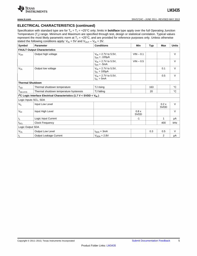
ELECTRICAL CHARACTERISTICSSpecification with standard type are for TA = TJ = +25°C only; limits in boldface type apply over the full Operating JunctionTemperature (TJ) range. Minimum and Maximum are specified through test, design or statistical correlation. Typical valuesrepresent the most likely parametric norm at TJ = +25°C, and are provided for reference purposes only. Unless otherwisestated the following conditions apply: VIN = 5V and VOUT – VIN = 3V.
Symbol Parameter Conditions Min Typ Max Units
Supply Characteristics
IIN IIN operating current No switching 5 10 mA
IIN-SD IIN Shutdown current VEN = 0V 8 30 µA
ISVDD SVDD standby supply current VSVDD = 5V, I2C Bus idle 1 µA
VINUVLO VIN under-voltage lock-out VIN decreasing 2.5 V
VINUVLO_hys VIN under-voltage lock-out hysteresis VIN increasing 0.2 V
Enable Input
VEN EN Pin input threshold VEN rising 0.8 x VIN V
VEN falling 0.2 x VIN V
IEN Enable Pull-up Current VEN = 0V 5 µA
Logic Inputs (RCTRL, GCTRL and BCTRL)
VCTRL CTRL pins input threshold VCTRL rising 1.35 V(VIN = 2.7V to 5.5V)
VCTRL falling 0.63(VIN = 2.7V to 5.5V)
Switching Characteristics
RDS-M-ON Main MOSFET RDS(ON) VGS(MAIN) =VIN = 5.0V 0.04 0.1 ΩISW(sink) = 100mA
RDS-S-ON Syn. MOSFET RDS(ON) VGS(SYN) = VOUT - 5.0V 0.06 0.2 ΩISW(source) = 100mA
Current Limit
ICL Peak current limit through main MOSFET 6 8.5 Athreshold
ON/OFF Timer
tON ON timer pulse width RRT = 499 kΩ 750 ns
tON-MIN ON timer minimum pulse width 80 ns
tOFF OFF timer minimum pulse width 155 ns
RGB Driver Characteristics (RLED, BLED and GLED)
RDS(RED) Red LED Switch RDS VOUT - VIN = 3.3V 0.1 0.2 ΩILED = 1.5AI2C code = 3FFh
RDS(BLU) Blue LED Switch RDS VOUT - VIN = 3.3V 0.1 0.2 ΩILED = 1.5AI2C code = 3FFh
RDS(GRN) Green LED Switch RDS VOUT - VIN = 3.3V 0.1 0.2 ΩILED = 1.5AI2C code = 3FFh
ILEDMAX Max. LED current (1) VIN = 4.5V to 5.5V, 2 A0°C ≤ TA ≤ 50°C
I1.5A,3FFh Current accuracy (3FFh) VIN = 2.7V to 5.5V 1.455 1.5 1.545 ARIREF = 16.5 kΩ, 1.425 1.575 AVOUT – VIN = 2.4V (RLED),
I1.5A,1FFh Current (1FFh) 0.8 A3.3V (GLED/BLED)
I1.5A,001h Current (001h) 1.2 mA
(1) Maximum LED current measured at VIN = 4.5V to 5.5V with heat sink on top of LM3435 with no air flow at 0°C ≤ TA ≤ 50°C. Operatingconditions differ from the above is not ensured.
4 Submit Documentation Feedback Copyright © 2011–2013, Texas Instruments Incorporated
Product Folder Links: LM3435
LM3435
www.ti.com SNVS724C –JUNE 2011–REVISED MAY 2013
ELECTRICAL CHARACTERISTICS (continued)Specification with standard type are for TA = TJ = +25°C only; limits in boldface type apply over the full Operating JunctionTemperature (TJ) range. Minimum and Maximum are specified through test, design or statistical correlation. Typical valuesrepresent the most likely parametric norm at TJ = +25°C, and are provided for reference purposes only. Unless otherwisestated the following conditions apply: VIN = 5V and VOUT – VIN = 3V.
Symbol Parameter Conditions Min Typ Max Units
FAULT Output Characteristics
VOH Output high voltage VIN = 2.7V to 5.5V, VIN – 0.1 VIOH = -100µA
VIN = 2.7V to 5.5V, VIN – 0.5 VIOH = -5mA
VOL Output low voltage VIN = 2.7V to 5.5V, 0.1 VIOL = 100µA
VIN = 2.7V to 5.5V, 0.5 VIOL = 5mA
Thermal Shutdown
TSD Thermal shutdown temperature TJ rising 163 °C
TSD-HYS Thermal shutdown temperature hysteresis TJ falling 20 °C
I2C Logic Interface Electrical Characteristics (1.7 V < SVDD < VIN )
Logic Inputs SCL, SDA
VIL Input Low Level 0.2 x VSVDD
VIH Input High Level 0.8 x VSVDD
IL Logic Input Current -1 1 µA
fSCL Clock Frequency 400 kHz
Logic Output SDA
VOL Output Low Level ISDA = 3mA 0.3 0.5 V
IL Output Leakage Current VSDA = 2.8V 2 µA
Copyright © 2011–2013, Texas Instruments Incorporated Submit Documentation Feedback 5
Product Folder Links: LM3435
2 3 4 5 6
30
40
50
60
70
80
90
RD
S-S
-ON
(m
)
VIN(V)
125°C
25°C
-40°C
5 15 25 35 45 55
0.0
0.5
1.0
1.5
2.0
2.5
I LE
Dx(
A)
RIREFx(k )
2 3 4 5 6
0
5
10
15
20
25
I SV
DD
(nA
)
VSVDD(V)
125°C
25°C
-40°C
2 3 4 5 6
20
30
40
50
60
70
RD
S-M
-ON
(m
)
VIN(V)
125°C
25°C
-40°C
2 3 4 5 6
0
2
4
6
8
10
12
I IN-S
D(
A)
VIN(V)
-40°C
25°C125°C
2 3 4 5 6
3.0
3.5
4.0
4.5
5.0
5.5
6.0
I IN(m
A)
VIN(V)
125°C
25°C
-40°C
LM3435
SNVS724C –JUNE 2011–REVISED MAY 2013 www.ti.com
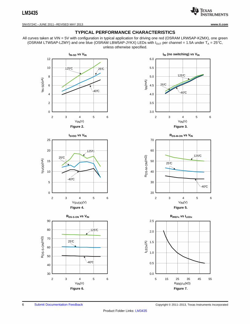
TYPICAL PERFORMANCE CHARACTERISTICSAll curves taken at VIN = 5V with configuration in typical application for driving one red (OSRAM LRW5AP-KZMX), one green
(OSRAM LTW5AP-LZMY) and one blue (OSRAM LBW5AP-JYKX) LEDs with IOUT per channel = 1.5A under TA = 25°C,unless otherwise specified.
IIN-SD vs VIN IIN (no switching) vs VIN
Figure 2. Figure 3.
ISVDD vs VIN RDS-M-ON vs VIN
Figure 4. Figure 5.
RDS-S-ON vs VIN RIREFx vs ILEDx
Figure 6. Figure 7.
6 Submit Documentation Feedback Copyright © 2011–2013, Texas Instruments Incorporated
Product Folder Links: LM3435
2 3 4 5 6
1.46
1.48
1.50
1.52
1.54
I LE
D(B
LU)(
A)
VIN(V)
125°C
25°C
-40°C
2 3 4 5 6
40
60
80
100
120
140
160
RD
S(B
LU)(
m
)
VIN(V)
125°C
25°C
-40°C
2 3 4 5 6
1.46
1.48
1.50
1.52
1.54
I LE
D(G
RN
)(A
)
VIN(V)
125°C-40°C
25°C
2 3 4 5 6
40
60
80
100
120
140
160
RD
S(G
RN
)(m
)
VIN(V)
125°C
25°C
-40°C
2 3 4 5 6
1.46
1.48
1.50
1.52
1.54
I LE
D(R
ED
)(A
)
VIN(V)
125°C
25°C
-40°C
2 3 4 5 6
40
60
80
100
120
140
160
RD
S(R
ED
)(m
)
VIN(V)
125°C
25°C
-40°C
LM3435
www.ti.com SNVS724C –JUNE 2011–REVISED MAY 2013
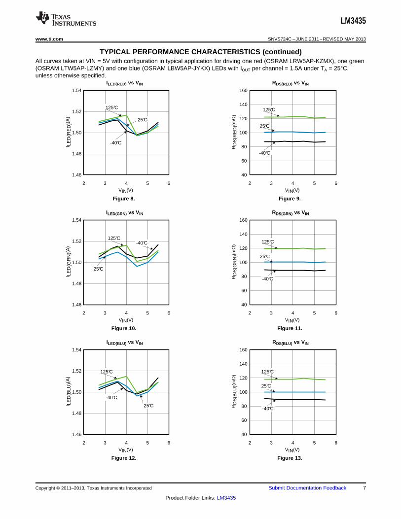
TYPICAL PERFORMANCE CHARACTERISTICS (continued)All curves taken at VIN = 5V with configuration in typical application for driving one red (OSRAM LRW5AP-KZMX), one green(OSRAM LTW5AP-LZMY) and one blue (OSRAM LBW5AP-JYKX) LEDs with IOUT per channel = 1.5A under TA = 25°C,unless otherwise specified.
ILED(RED) vs VIN RDS(RED) vs VIN
Figure 8. Figure 9.
ILED(GRN) vs VIN RDS(GRN) vs VIN
Figure 10. Figure 11.
ILED(BLU) vs VIN RDS(BLU) vs VIN
Figure 12. Figure 13.
Copyright © 2011–2013, Texas Instruments Incorporated Submit Documentation Feedback 7
Product Folder Links: LM3435
2 3 4 5 6
50
60
70
80
90
100
BLU
E E
FF
ICIE
NC
Y,
BLU
(%)
VIN(V)
2 3 4 5 6
50
60
70
80
90
100
RE
D E
FF
ICIE
NC
Y,
RE
D(%
)
VIN(V)2 3 4 5 6
50
60
70
80
90
100
GR
EE
N E
FF
ICIE
NC
Y,
GR
N(%
)
VIN(V)
LM3435
SNVS724C –JUNE 2011–REVISED MAY 2013 www.ti.com
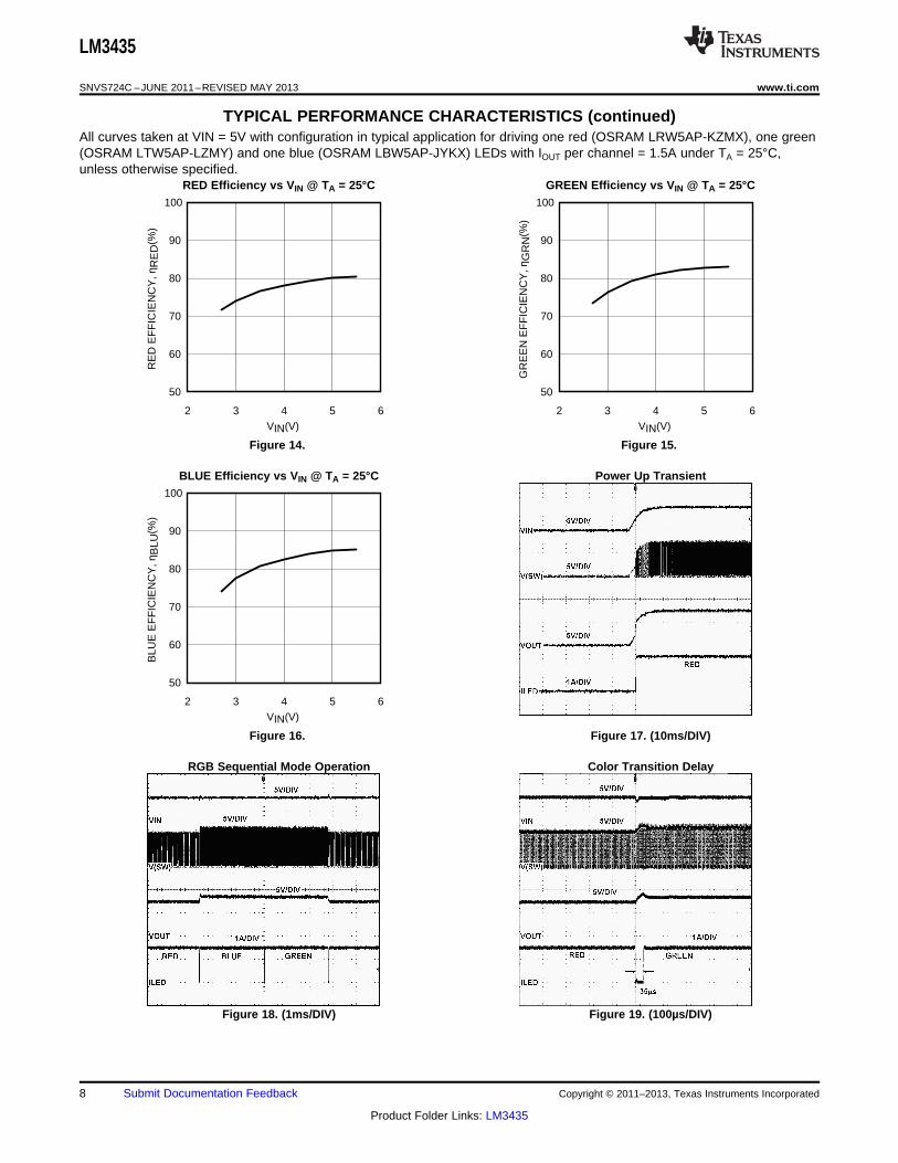
TYPICAL PERFORMANCE CHARACTERISTICS (continued)All curves taken at VIN = 5V with configuration in typical application for driving one red (OSRAM LRW5AP-KZMX), one green(OSRAM LTW5AP-LZMY) and one blue (OSRAM LBW5AP-JYKX) LEDs with IOUT per channel = 1.5A under TA = 25°C,unless otherwise specified.
RED Efficiency vs VIN @ TA = 25°C GREEN Efficiency vs VIN @ TA = 25°C
Figure 14. Figure 15.
BLUE Efficiency vs VIN @ TA = 25°C Power Up Transient
Figure 16. Figure 17. (10ms/DIV)
RGB Sequential Mode Operation Color Transition Delay
Figure 18. (1ms/DIV) Figure 19. (100µs/DIV)
8 Submit Documentation Feedback Copyright © 2011–2013, Texas Instruments Incorporated
Product Folder Links: LM3435
RGB Current RegulatorAnd Logic Control
Gm Sample& Hold
Comp
Gm
Gm
MUX
I2C Interface
Logic
10 bit10 bit10 bit
IGRN IBLU IRED
Bias and Vref
Gint
Bint
Rint
Flyback Converter
Control Logic
GintBintRint
L.S. Driver
H.S. Driver
ON-timer
OFF-timer
VOUT
RT
EN
PGND
IREFR
IREFB
IREFG
SCLK
SDATA
SVDD
FAULT
RCTRL
BCTRL
GCTRL
GLED BLED RLED VIN SW
GND
CR
CB
CG
SGND
SENG,B,RSENG
SENB
SENR
IREFG,B,R
IREFG
IREFB
IREFRVREF
Comp
Comp
Ch. Select
VFB
Feedback
Sample& Hold
Sample& Hold
LM3435
www.ti.com SNVS724C –JUNE 2011–REVISED MAY 2013
SIMPLIFIED FUNCTIONAL BLOCK DIAGRAM
OPERATION DESCRIPTION
INTRODUCTION
The LM3435 is a sequential LED driver for portable and pico projectors. The device is integrated with three highcurrent regulators, low side MOSFETs and a synchronous flyback DC-DC converter. Only single LED can beenabled at any given time. The DC-DC converter quickly adjusts the output voltage to an optimal level based oneach LED’s forward voltage. This minimizes the power dissipation at the current regulators and maximizes thesystem efficiency. The I2C compatible synchronous serial interface provides access to the programmablefunctions and registers of the device. I2C protocol uses a two-wire interface for bi-directional communicationsbetween the devices connected to the bus. The two interface lines are the Serial Data Line (SDA), and the SerialClock Line (SCL). These lines should be connected to a positive supply, via a pull-up resistor and remain HIGHeven when the bus is idle. Every device on the bus is assigned an unique address and acts as either a Master ora Slave depending on whether it generates or receives the serial clock (SCL).
SYNCHRONOUS FLYBACK CONVERTER
The LM3435 integrates a synchronous flyback DC-DC converter to power the three-channel current regulator.The LEDs are connected across VOUT of the flyback converter and VIN through an internal power MOSFETconnecting to corresponding LED channel. The maximum current to LED is 2A and the maximum voltage acrossVOUT and VIN is limited at around 4.7V. The LM3435 integrates the main N-channel MOSFET, the synchronousP-channel MOSFET of the flyback converter and three N-channel MOSFETs as internal passing elementsconnecting to LED channels in order to minimize the solution components count and PCB space.
Copyright © 2011–2013, Texas Instruments Incorporated Submit Documentation Feedback 9
Product Folder Links: LM3435
LM3435
SNVS724C –JUNE 2011–REVISED MAY 2013 www.ti.com
The flyback converter of LM3435 employs a proprietary Projected On-Time (POT) control scheme to determinethe on-time of the main N-channel MOSFET with respect to the input and output voltages together with anexternal switching frequency setting resistor connected to RT pin, RRT. POT control use information of the currentpassing through RRT from VOUT, voltage information of VOUT and VIN to find an appropriate on-time for thecircuit operations. During the on-time period, the inductor connecting to the flyback converter is charged up andthe output capacitor is discharged to supply power to the LED. A cycle-by-cycle current limit of typical 6A isimposed on the main N-channel MOSFET for protection. After the on-time period, the main N-channel MOSFETis turned off and the synchronous P-channel MOSFET is turned on in order to discharge the inductor. The offstate will last until VOUT is dropped below a reference voltage. Such reference voltage is derived from therequired LED current to be regulated at a particular LED channel. The flyback converter under POT control canmaintain a fairly constant switching frequency that depends mainly on value of the resistor connected acrossVOUT and RT pins, RRT. The relationship between the flyback converter switching frequency, FSW and RRT isapproximated by the following relationship:
RRT in Ω and FSW in kHz (1)
In addition, POT control requires no external compensation and achieves fast transient response of the outputvoltage changes that perfectly matches the requirements of a sequential RGB LED driver. The POT flybackconverter only operates at Continuous Conduction Mode. Dead-time between main MOSFET and synchronousMOSFET switching is adaptively controlled by a minimum non-overlap timer to prevent current shoot through.Initial VOUT will be regulated at around 3.2V to 3.5V above VIN before any control signals being turned on.Three small capacitors connected to CR, CG and CB pins are charged by an internal current source and act assoft-start capacitors of the flyback converter during start-up. Once initial voltage of VOUT is settled, thecapacitors will be used as a memory element to store the VOUT information for each channel respectively. Thisinformation will be used for VOUT regulation of respective LED channel during channel switching. In between thechannel switching, a small I2C programmable blank out time of 5 µs to 35 µs is inserted so that the LED currentis available after the correct VOUT for the color is stabilized. This control scheme ensures the minimal voltageheadroom for different color LED and hence best conversion efficiency can be achieved.
HIGH CURRENT REGULATORS
The LM3435 contains three internal current regulators powered by the output of the synchronous FlybackConverter, VOUT. Three low side power MOSFETs are included. These current regulators control the currentsupplied to the LED channels individually and maintain accurate current regulation by internal feedback andcontrol mechanism. The regulation is achieved by a Gm-C circuit comparing the sensing voltage of the internalpassing N-channel MOSFET and an internal LED current reference voltage generated from the externalreference current setting resistor, RIREFx connect to IREFG, IREFB or IREFR pin, of the corresponding LEDchannel. The nominal maximum LED current is governed by the equation in below:
RIREFx in Ω and ILEDx in Ampere (2)
The LED current setting can be in the range of 0.5A up to 2A maximum. The nominal maximum of the device is1.5A and for applications need higher than 1.5A LED current, VIN and thermal constrains must be complied. Theactual LED current can be adjusted on-the-fly by the internal ten bits register for individual channel. The contentof these registers are user programmable via I2C bus connection. The user can control the LED output currenton-the-fly during normal operation. The resolution is 1 out of 1024 part of the LED current setting. The user canprogram the registers in the range of 1(001H) to 1023(3FFH) for each channel independently, provided theconverter is not entered the Discontinuous Conduction Mode. Whenever the converter operation entered theDiscontinuous Conduction Mode, the regulation will be deteriorated. A value of “0” may cause false faultdetection, so it must be avoided.
10 Submit Documentation Feedback Copyright © 2011–2013, Texas Instruments Incorporated
Product Folder Links: LM3435
BLUEGREEN
GCTRL
BCTRL
RCTRL
RED BLUE GREEN
IGLED
IBLED
IRLED
Green Transition Delay
Blue Transition Delay
Red Transition Delay
RCTRL
GCTRL
BCTRL
GREENRED BLUE
1/3 1/31/3
1/FPWM
GREENRED BLUE
1/3 1/31/3
1/FPWM
LM3435
www.ti.com SNVS724C –JUNE 2011–REVISED MAY 2013
SEQUENTIAL MODE RGB TIMING
LM3435 is a sequential mode RGB driver dedicatedly designed for pico and portable projector applications. Byusing this device, the system only require one power driver stage for three color LEDs. With LM3435, only singleLED can be enabled at any given time period and the DC-DC converter can quickly adjusts the output voltage toan optimized level by controlling the current flowing into the respective LED channel. This approach minimizesthe power dissipation of the internal current regulator and effectively maximizes the system efficiency. Timing ofthe RGB LEDs depends solely on the RCTRL, GCTRL and BCTRL inputs. The Timing Chart in below shows atypical timing of two cycles of even RGB scan. In real applications, the RGB sequence is totally controlled by thesystem or the video processor. It’s not mandatory to follow the simple RGB sequence, but for any changeinstructed by the I2C control will only take place at the falling edge of the corresponding CTRL signal.
Figure 20. RGB Control Signals Timing Chart
PRIORITIES OF LED CONTROL SIGNALS
The LM3435 does not support color overlapping mode operation. At any instant, only one LED will be enabledeven overlapping control signals applied to the control inputs. The decision logics of the device determine whichLED channel should be enabled in case overlapping control signals are detected at the control inputs. TheGREEN channel has the higher priority over BLUE channel and the RED channel has the lowest priority.However, if a low priority channel is already turned on before the high priority channel control signal comes in,the low priority channel will continue to take the control until the control signal ceased. The timing diagram inbelow illustrates some typical cases during operation.
Figure 21. Priorities of LED Control Signals
Copyright © 2011–2013, Texas Instruments Incorporated Submit Documentation Feedback 11
Product Folder Links: LM3435
LM3435
SNVS724C –JUNE 2011–REVISED MAY 2013 www.ti.com
LED OPEN FAULT REPORTING
The fly-back converter tries to keep VOUT to the forward voltage required by the LED with the desired LEDcurrent output. However, if the LED channel is being opened no matter it is due to LED failure or no connection,the fly-back converter will limit the VOUT voltage at around 4.7V above VIN. Once such voltage is achieved, anopen-fault-suspect signal will go high. If this open-fault-suspect signal is being detected at 3 consecutive fallingedges of the opened channel control signal, “Fault” pin will be latched high and the corresponding channel openfault will be reported through I2C. The open fault report can be removed either by pulling EN pin low for less than100ns (a true shutdown will be triggered if the negative pulse on EN is more than 100ns) or by writing a “0” to “bit0” of the I2C register ”05h”. The “Fault” pin will be cleared and the I2C fault register will be reset. In order toreinstate the fault reporting feature, the system need to write a “1” to “bit 0” of the I2C register “05h”.
LED SHORT FAULT REPORTING
If the VOUT is prohibited to regulate at a potential higher than 1.5V above VIN at a LED channel, such LED isconsidered being shorted and a short-fault-suspect signal will go high. If this short-fault-suspect signal is beingdetected at 3 consecutive falling edges of the shorted channel control signal, “Fault” pin will be latched high andthe corresponding channel short fault will be reported through I2C. The short fault report can be removed eitherby pulling EN pin low for less than 100ns (a true shutdown will be triggered if the negative pulse on EN is morethan 100ns) or by writing a “0” to “bit 0” of the I2C register ”05h”. The “Fault” pin will be cleared and the I2C faultregister will be reset. In order to reinstate the fault reporting feature, the system need to write a “1” to “bit 0” ofthe I2C register “05h”. Persistently short of LED can cause permanent damage to the device. Whenever the shortfault is detected, the system should turn off the faulty channel immediately by pulling the corresponding PWMcontrol pin to GND.
THERMAL SHUTDOWN
Internal thermal shutdown circuitry is included to protect the device in the event that the maximum junctiontemperature is exceeded. The threshold for thermal shutdown in LM3435 is around 160°C and it will be resumedto normal operation again once the temperature cools down to below around 140°C.
I2C Compatible Interface
INTERFACE BUS OVERVIEW
The I2C compatible synchronous serial interface provides access to the programmable functions and registers onthe device. This protocol uses a two-wire interface for bi-directional communications between the devicesconnected to the bus. The two interface lines are the Serial Data Line (SDA), and the Serial Clock Line (SCL).These lines should be connected to a positive supply, via a pull-up resistor and remain HIGH even when the busis idle. Every device on the bus is assigned a unique address and acts as either a Master or a Slave dependingon whether it generates or receives the serial clock (SCL).
DATA TRANSACTIONS
One data bit is transferred during each clock pulse. Data is sampled during the high state of the serial clock(SCL). Consequently, throughout the clock’s high period, the data should remain stable. Any changes on theSDA line during the high state of the SCL and in the middle of a transaction, aborts the current transaction. Newdata should be sent during the low SCL state. This protocol permits a single data line to transfer bothcommand/control information and data using the synchronous serial clock.
12 Submit Documentation Feedback Copyright © 2011–2013, Texas Instruments Incorporated
Product Folder Links: LM3435
ADR6Bit7
ADR5bit6
ADR4bit5
ADR3bit4
ADR2bit3
ADR1bit2
ADR0bit1
R/Wbit0
MSB LSB
I2C SLAVE address (chip address)
SDA
SCLS P
START condition STOP condition
SCL
SDA
datachangeallowed
datavalid
datachangeallowed
datavalid
datachangeallowed
LM3435
www.ti.com SNVS724C –JUNE 2011–REVISED MAY 2013
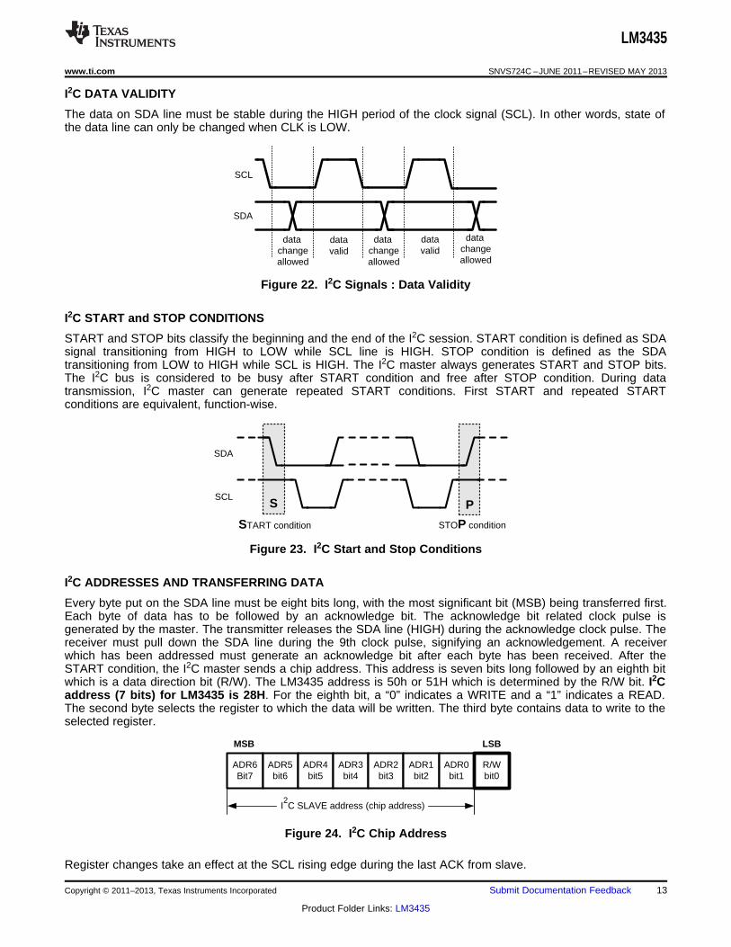
I2C DATA VALIDITY
The data on SDA line must be stable during the HIGH period of the clock signal (SCL). In other words, state ofthe data line can only be changed when CLK is LOW.
Figure 22. I2C Signals : Data Validity
I2C START and STOP CONDITIONS
START and STOP bits classify the beginning and the end of the I2C session. START condition is defined as SDAsignal transitioning from HIGH to LOW while SCL line is HIGH. STOP condition is defined as the SDAtransitioning from LOW to HIGH while SCL is HIGH. The I2C master always generates START and STOP bits.The I2C bus is considered to be busy after START condition and free after STOP condition. During datatransmission, I2C master can generate repeated START conditions. First START and repeated STARTconditions are equivalent, function-wise.
Figure 23. I2C Start and Stop Conditions
I2C ADDRESSES AND TRANSFERRING DATA
Every byte put on the SDA line must be eight bits long, with the most significant bit (MSB) being transferred first.Each byte of data has to be followed by an acknowledge bit. The acknowledge bit related clock pulse isgenerated by the master. The transmitter releases the SDA line (HIGH) during the acknowledge clock pulse. Thereceiver must pull down the SDA line during the 9th clock pulse, signifying an acknowledgement. A receiverwhich has been addressed must generate an acknowledge bit after each byte has been received. After theSTART condition, the I2C master sends a chip address. This address is seven bits long followed by an eighth bitwhich is a data direction bit (R/W). The LM3435 address is 50h or 51H which is determined by the R/W bit. I2Caddress (7 bits) for LM3435 is 28H. For the eighth bit, a “0” indicates a WRITE and a “1” indicates a READ.The second byte selects the register to which the data will be written. The third byte contains data to write to theselected register.
Figure 24. I2C Chip Address
Register changes take an effect at the SCL rising edge during the last ACK from slave.
Copyright © 2011–2013, Texas Instruments Incorporated Submit Documentation Feedback 13
Product Folder Links: LM3435
SDA
SCL
1
8
2
3
7 6
5
8
10
4 9
1 7
ack from slave
msb Chip Address lsb
ack from slave
w msb Register Add lsb rs r msb DATA lsb stop
ack from slave nack from masterrepeated start data from slave
start id = 28h w ack addr = h00 ack rs r ack Address 00h data nack stop
msb Chip Address lsb
id = 28h
start
SCL
SDA
start msb Chip Address lsb w ack msb Register Add lsb ack msb DATA lsb ack stop
ack from slave ack from slave ack from slave
SCL
SDA
start id = 28h w ack addr = 02h ack ackaddress 02h data stop
LM3435
SNVS724C –JUNE 2011–REVISED MAY 2013 www.ti.com
w = write (SDA = “0”)r = read (SDA = “1”)ack = acknowledge (SDA pulled down by either master or slave)rs = repeated startid = 7-bit chip address, 50H (ADDR_SEL=0) or 51H (ADDR_SEL=1) for LM3435.
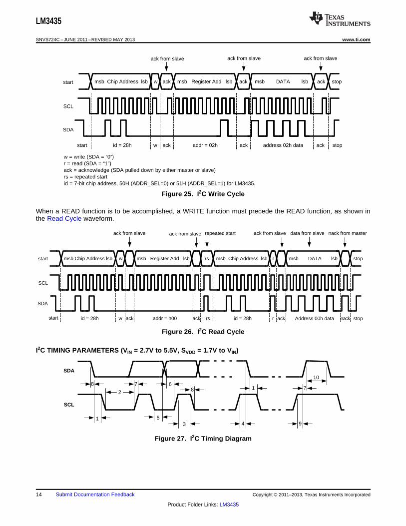
Figure 25. I2C Write Cycle
When a READ function is to be accomplished, a WRITE function must precede the READ function, as shown inthe Read Cycle waveform.
Figure 26. I2C Read Cycle
I2C TIMING PARAMETERS (VIN = 2.7V to 5.5V, SVDD = 1.7V to VIN)
Figure 27. I2C Timing Diagram
14 Submit Documentation Feedback Copyright © 2011–2013, Texas Instruments Incorporated
Product Folder Links: LM3435
LM3435
www.ti.com SNVS724C –JUNE 2011–REVISED MAY 2013
Symbol Parameter Limit (1) Units
Min Max
1 Hold Time (repeated) START Condition 0.6 µs
2 Clock Low Time 1.3 µs
3 Clock High Time 600 ns
4 Setup Time for a Repeated START Condition 600 ns
5 Data Hold Time (Output direction) 300 ns
5 Data Hold Time (Input direction) 0 ns
6 Data Setup Time 100 ns
7 Rise Time of SDA and SCL 20+0.1Cb 300 ns
8 Fall Time of SDA and SCL 15+0.1Cb 300 ns
9 Set-up Time for STOP condition 600 ns
10 Bus Free Time between a STOP and a START Condition 1.3 µs
Cb Capacitive Load for Each Bus Line 10 200 pF
(1) Note: Data specified by design.
I2C REGISTER DETAILS
The I2C bus interacts with the LM3435 to realize the features of LED current program inter-color delay timeprogram and Fault reporting function. The operation of these functions requires the writing and reading of theinternal registers of the LM3435. In below is the master register map of the device.
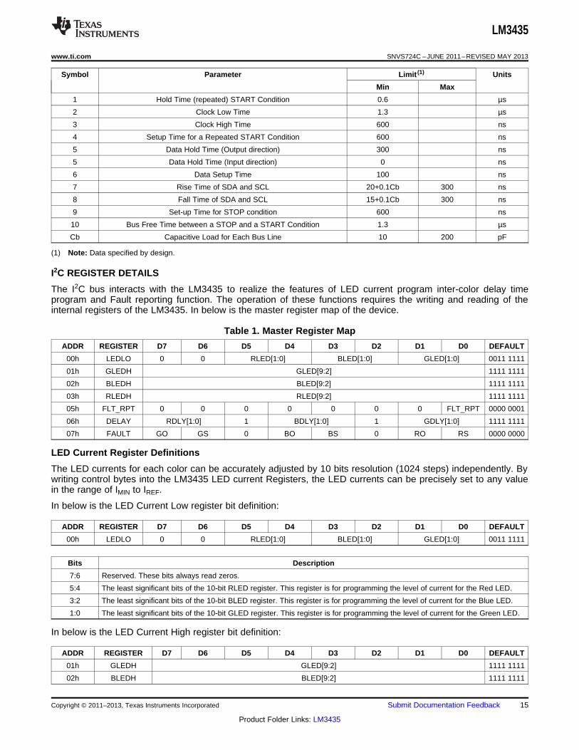
Table 1. Master Register Map
ADDR REGISTER D7 D6 D5 D4 D3 D2 D1 D0 DEFAULT
00h LEDLO 0 0 RLED[1:0] BLED[1:0] GLED[1:0] 0011 1111
01h GLEDH GLED[9:2] 1111 1111
02h BLEDH BLED[9:2] 1111 1111
03h RLEDH RLED[9:2] 1111 1111
05h FLT_RPT 0 0 0 0 0 0 0 FLT_RPT 0000 0001
06h DELAY RDLY[1:0] 1 BDLY[1:0] 1 GDLY[1:0] 1111 1111
07h FAULT GO GS 0 BO BS 0 RO RS 0000 0000
LED Current Register Definitions
The LED currents for each color can be accurately adjusted by 10 bits resolution (1024 steps) independently. Bywriting control bytes into the LM3435 LED current Registers, the LED currents can be precisely set to any valuein the range of IMIN to IREF.
In below is the LED Current Low register bit definition:
ADDR REGISTER D7 D6 D5 D4 D3 D2 D1 D0 DEFAULT
00h LEDLO 0 0 RLED[1:0] BLED[1:0] GLED[1:0] 0011 1111
Bits Description
7:6 Reserved. These bits always read zeros.
5:4 The least significant bits of the 10-bit RLED register. This register is for programming the level of current for the Red LED.
3:2 The least significant bits of the 10-bit BLED register. This register is for programming the level of current for the Blue LED.
1:0 The least significant bits of the 10-bit GLED register. This register is for programming the level of current for the Green LED.
In below is the LED Current High register bit definition:
ADDR REGISTER D7 D6 D5 D4 D3 D2 D1 D0 DEFAULT
01h GLEDH GLED[9:2] 1111 1111
02h BLEDH BLED[9:2] 1111 1111
Copyright © 2011–2013, Texas Instruments Incorporated Submit Documentation Feedback 15
Product Folder Links: LM3435
LM3435
SNVS724C –JUNE 2011–REVISED MAY 2013 www.ti.com
ADDR REGISTER D7 D6 D5 D4 D3 D2 D1 D0 DEFAULT
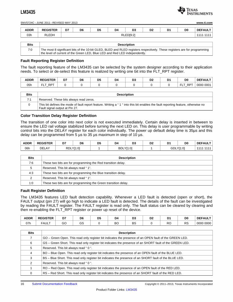
03h RLEDH RLED[9:2] 1111 1111
Bits Description
7:0 The most 8 significant bits of the 10-bit GLED, BLED and RLED registers respectively. These registers are for programmingthe level of current of the Green LED, Blue LED and Red LED independently.
Fault Reporting Register Definition
The fault reporting feature of the LM3435 can be selected by the system designer according to their applicationneeds. To select or de-select this feature is realized by writing one bit into the FLT_RPT register.
ADDR REGISTER D7 D6 D5 D4 D3 D2 D1 D0 DEFAULT
05h FLT_RPT 0 0 0 0 0 0 0 FLT_RPT 0000 0001
Bits Description
7:1 Reserved. These bits always read zeros.
0 This bit defines the mode of fault report feature. Writing a “ 1 “ into this bit enables the fault reporting feature, otherwise noFault signal output at Pin 27.
Color Transition Delay Register Definition
The transition of one color into next color is not executed immediately. Certain delay is inserted in between toensure the LED rail voltage stabilized before turning the next LED on. This delay is user programmable by writingcontrol bits into the DELAY register for each color individually. The power up default delay time is 35µs and thisdelay can be programmed from 5 µs to 35 µs maximum in step of 10 µs.
ADDR REGISTER D7 D6 D5 D4 D3 D2 D1 D0 DEFAULT
06h DELAY RDLY[1:0] 1 BDLY[1:0] 1 GDLY[1:0] 1111 1111
Bits Description
7:6 These two bits are for programming the Red transition delay.
5 Reserved. This bit always read “ 1“.
4:3 These two bits are for programming the Blue transition delay.
2 Reserved. This bit always read “ 1“.
1:0 These two bits are for programming the Green transition delay.
Fault Register Definition
The LM3435 features LED fault detection capability. Whenever a LED fault is detected (open or short), theFAULT output (pin 27) will go high to indicate a LED fault is detected. The details of the fault can be investigatedby reading the FAULT register. The FAULT register is read only. The fault status can be cleared by clearing andthen re-enabling the FLT_RPT register or power up reset of the device.
ADDR REGISTER D7 D6 D5 D4 D3 D2 D1 D0 DEFAULT
07h FAULT GO GS 0 BO BS 0 RO RS 0000 0000
Bits Description
7 GO – Green Open. This read only register bit indicates the presence of an OPEN fault of the GREEN LED.
6 GS – Green Short. This read only register bit indicates the presence of an SHORT fault of the GREEN LED.
5 Reserved. This bit always read “ 0 “.
4 BO – Blue Open. This read only register bit indicates the presence of an OPEN fault of the BLUE LED.
3 BS – Blue Short. This read only register bit indicates the presence of an SHORT fault of the BLUE LED.
2 Reserved. This bit always read “ 0 “.
1 RO – Red Open. This read only register bit indicates the presence of an OPEN fault of the RED LED.
0 RS – Red Short. This read only register bit indicates the presence of an SHORT fault of the RED LED.
16 Submit Documentation Feedback Copyright © 2011–2013, Texas Instruments Incorporated
Product Folder Links: LM3435
LM3435
www.ti.com SNVS724C –JUNE 2011–REVISED MAY 2013
Design Procedures
This section presents a design example of a typical pico projector application. By using LM3435, the systemrequires only single DC-DC converter to drive three color LEDs instead of using three DC-DC converters withconventional design. The suggested approach not only saves components cost, but also releases invaluablePCB space to the system and enhances system reliability. The handy projector is powered by a single lithiumbattery cell or a 5Vdc wall mount adaptor. The key specifications of the design are as in below:• Supply voltage range, VIN = 2.7V to 5.5V• Preset LED current per channel, ILED = 1.5A• Minimum LED current per channel, ILED(MIN) = 600mA• Maximum LED forward voltage drop, VLED = 3.5V at 1.5A• Flyback converter switching Frequency, FSW = ~500kHz
SETTING THE FLYBACK CONVERTER SWITCHING FREQUENCY, FSW
The LM3435 employs a proprietary Projected On-Time (POT) control scheme, the switching frequency, FSW ofthe converter is simply set by an external resistor, RRT across RT pin of LM3435 and VOUT of the converter. Theflyback converter under POT control can maintain a fairly constant switching frequency that depends mainly onthe value of RRT. The relationship between the flyback converter switching frequency, FSW and RRT isapproximated by the following relationship:
RRT in Ω and FSW in kHz (3)
In order to set the flyback converter switching frequency, FSW to 500kHz, the value of RRT can be calculated as inbelow:
(4)
A standard resistor value of 499kΩ can be used in place and the period of switching, TSW is about 2µs.
SETTING THE NOMINAL LED CURRENT
The nominal LED current of the LEDs are set by resistors connected to IREFR, IREFG and IREFB pins. Thecurrent for each channel can be set individually and it is not mandatory that all channel currents are the same.Just for simplicity, we assume all channels are set to 1.5A in this example. The LED current and the value ofRIREFR, RIREFG and RIREFB is governed by the following equation.
RIREFx in Ω and ILEDx in Ampere (5)
The resistance value for the current setting resistors is calculated as in below:
(6)
In order to achieve the required LED current accuracy, high quality resistors with tolerance not higher than +/-1%are recommended.
Copyright © 2011–2013, Texas Instruments Incorporated Submit Documentation Feedback 17
Product Folder Links: LM3435
t
TON
ILripple(MAX)
ILripple(MIN)
IL(AVG)
TOFF(TSW x D) (TSW x (1-D))
Slope =VIN
L
IL
VL = VIN - VSW
VIN
VLED
0
0
t
Slope =-VLED
L
LM3435
SNVS724C –JUNE 2011–REVISED MAY 2013 www.ti.com
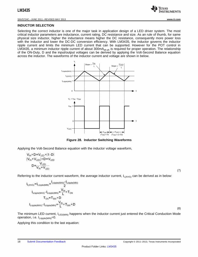
INDUCTOR SELECTION
Selecting the correct inductor is one of the major task in application design of a LED driver system. The mostcritical inductor parameters are inductance, current rating, DC resistance and size. As an rule of thumb, for samephysical size inductor, higher the inductance means higher the DC resistance, consequently more power losswith the inductor and lower the DC-DC conversion efficiency. With LM3435, the inductor governs the inductorripple current and limits the minimum LED current that can be supported. However for the POT control inLM3435, a minimum inductor ripple current of about 300mApk-pk is required for proper operation. The relationshipof the ON-Duty, D and the input/output voltages can be derived by applying the Volt-Second Balance equationacross the inductor. The waveforms of the inductor current and voltage are shown in below.
Figure 28. Inductor Switching Waveforms
Applying the Volt-Second Balance equation with the inductor voltage waveform,
(7)
Referring to the inductor current waveform, the average inductor current, IL(AVG) can be derived as in below:
(8)
The minimum LED current, ILED(MIN) happens when the inductor current just entered the Critical Conduction Modeoperation, i.e. ILripple(MIN)=0.
Applying this condition to the last equation:
18 Submit Documentation Feedback Copyright © 2011–2013, Texas Instruments Incorporated
Product Folder Links: LM3435
LM3435
www.ti.com SNVS724C –JUNE 2011–REVISED MAY 2013
(9)
The relationship of the LED current, ILED and the average inductor current, IL(AVG) is shown in below:
(10)
By combining last two equations, the minimum LED current, ILED(MIN) can be calculated as in below:
(11)
By rearranging the terms, the inductance, L required for any specific minimum LED current, ILED(MIN) can be foundwith the equation in below:
(12)
From the equation, it can be noted that for lower minimum LED current, the inductance required will be higher.As mentioned in before, higher the inductance means higher DC resistance in same size inductor. Additionally,the POT control in LM3435, a minimum inductor ripple current is required to maintain proper operation. Therestrictions limit the lowest current can be programed by I2C control.
In this example, the ILED(MIN)=600mA and the highest ripple will happen when the input voltage is maximum, i.e.VIN=5.5V. The ON Duty, D with average LED forward voltage of 3.5V is calculated in below:
(13)
The required inductance for this case is:
(14)
A standard inductance value of 2.2µH is suggested and the minimum LED current, ILED(MIN) is about 595mA @VIN=5.5V.
Other than the inductance, the worst case inductor current, IL(MAX) must be calculated so that an inductor withappropriate saturation current level can be specified. The maximum inductor current, IL(MAX) can be calculatedwith the equation in below:
(15)
The highest inductor current occurs when the input voltage is minimum, i.e. VIN=2.7V. The ON Duty, D for thiscondition can be calculated as in below:
(16)
The maximum inductor current, IL(MAX) is calculated in below:
(17)
Copyright © 2011–2013, Texas Instruments Incorporated Submit Documentation Feedback 19
Product Folder Links: LM3435
LM3435
SNVS724C –JUNE 2011–REVISED MAY 2013 www.ti.com
The calculated maximum inductor current is 4.1A, however the inductance can drop as temperature rise. In orderto accommodate all possible variations, an inductor with saturation current specification not less than 5A issuggested.
INPUT CAPACITORS SELECTION
Input capacitors are required for all supply input pins to ensure that VIN does not drop excessively during highcurrent switching transients. LM3435 have supply input pins located in different sides of the device. Individualcapacitors are needed for the supply input pins locally. All capacitors must be placed as close as possible to thesupply input pins and have low impedance return ground path to the device grounds and back to supply ground.Capacitors CIN1 and CIN2 are the main input capacitors and additionally, CIN3 is added to de-couple highfrequency interference. The capacitance for CIN1 and CIN2 is recommended in the range of 22μF to 47µF andCIN3 is 0.1µF. Compact applications normally have stringent space limitations, small size surface mountcapacitors are usually preferred. Low ESR Multi-Layer Ceramic Capacitors (MLCC) are the best choices. MLCCcapacitors with X5R and X7R dielectrics are recommended for its low leakage and low capacitance variationagainst temperature and frequency.
OUTPUT CAPACITORS SELECTION
Two output capacitors are required with LM3435 configuration, one for VOUT to Ground, COUT2 and one for de-coupling the LED current ripple, COUT1. The LM3435 operates at frequencies high enough to allow the use ofMLCC capacitors without compromising transient response. Low ESR characteristic of the MLCC allow higherinductor ripple without significant increase of the output ripple. The capacitance recommended for COUT1 is 10µFand COUT2 is 22µF. Again, high quality MLCC capacitors with X5R and X7R dielectrics are recommended. Forcertain conditions, acoustic problem may be encountered with using MLCC, Low Acoustic Noise Type capacitorsare strongly recommended for all output capacitors. Alternatively, the acoustic noise can also be lowered byusing smaller size capacitors in parallel to achieve the required capacitance.
OTHER CAPACITORS SELECTION
Three small startup capacitors connected to CG, CB and CR pins are needed for proper operation. Thesuggested capacitance for CCR, CCG and CCB is 1nF. Also three capacitors connected to GLED, BLED and RLEDpins to protect the device from high transient stress due to the inductance of the connecting wires for the LEDs.The suggested capacitance for CG, CB and CR is 0.47µH. MLCC capacitors with X5R and X7R dielectrics arerecommended. All capacitors must be placed as close as possible to the device pins.
DIODE SELECTION
A schottky barrier diode is added across the SW and VOUT pins, equivalently, its across the internal P-channelMOSFET of the synchronous converter, that can help to improve the conversion efficiency by few percents. Avery low forward voltage and 1A rated forward current part is suggested in the schematic diagram. The keyselection criteria are the forward voltage and the rated forward current.
PCB LAYOUT CONSIDERATIONS
The performance of any switching converters depends as much upon the layout of the PCB as the componentselection. PCB layout considerations are therefore critical for optimum performance. The layout must be as neatand compact as possible, and all external components must be as close as possible to their associated pins. ThePGND connection to CIN and VOUT connection to COUT should be as short and direct as possible with thicktraces. The inductor should connect close to the SW pin with short and thick trace to reduce the potential electro-magnetic interference.
It is expected that the internal power elements of the LM3435 will produce certain amount of heat during normaloperation, good use of the PC board's ground plane can help considerably to dissipate heat. The exposed padon the bottom of the IC package can be soldered to a copper pad with thermal vias that can help to conduct theheat to the bottom side ground plane. The bottom side ground plane should be as large as possible.
20 Submit Documentation Feedback Copyright © 2011–2013, Texas Instruments Incorporated
Product Folder Links: LM3435
VO
UT
GLED
RLED
CG
CB
IREFR
IREFG
IREFB
VIN
1
2
3
4
5
21
FAULT
6
7
PG
ND
PG
ND
SW
SGND
CR
GNDB
CT
RL
SD
AT
A
SC
LK
GC
TR
L
SV
DD
RC
TR
L
DAP(PGND)
11 12 1817161513 14
22
23
24
25
26
27
36RIREFG
SDATASCLK
GCTRL
BCTRL
RCTRL
L1
COUT1
RRT
RED
GRN
BLU
CIN3
Vin
CCG
CCB
CCRS
W
PGND
SGND
8
9
BLED
GLED
BLED
RLEDV
OU
T
RT
35 34 33 32 31
SVDD
CSVDD
VIN
VIN
PG
ND
FAULT
SD1
COUT2
PGND
10
VIN
VIN
2019
EN
EN28
29
30VOUT
SW
40 39 38 37
VOUT
*RSDA *RSCK
I2C BUS
PWM ControlsAnd
GPIO Bus
CIN1
CIN2
GND
GND
CG
CB
CR
* RSDA, RSCK ± I2C Pull-high resistors
U1
10k 10k
1 PF/10V47 PF/10V
RIREFB
RIREFR
16.5k
16.5k
16.5k
1 nF/16V
1 nF/16V
1 nF/16V
47 PF/10V
0.1 PF/25V
499k
22 PF/16V
10 PF/16V2.2 PH/6A
RB160M-60
3 x 0.47 PF/25V
LM3435
www.ti.com SNVS724C –JUNE 2011–REVISED MAY 2013
SCHEMATIC OF THE EXAMPLE APPLICATION FOR PICO PROJECTOR
Copyright © 2011–2013, Texas Instruments Incorporated Submit Documentation Feedback 21
Product Folder Links: LM3435
LM3435
SNVS724C –JUNE 2011–REVISED MAY 2013 www.ti.com
REVISION HISTORY
Changes from Revision B (May 2013) to Revision C Page
• Changed layout of National Data Sheet to TI format .......................................................................................................... 21
22 Submit Documentation Feedback Copyright © 2011–2013, Texas Instruments Incorporated
Product Folder Links: LM3435
PACKAGE OPTION ADDENDUM
www.ti.com 2-May-2013
Addendum-Page 1
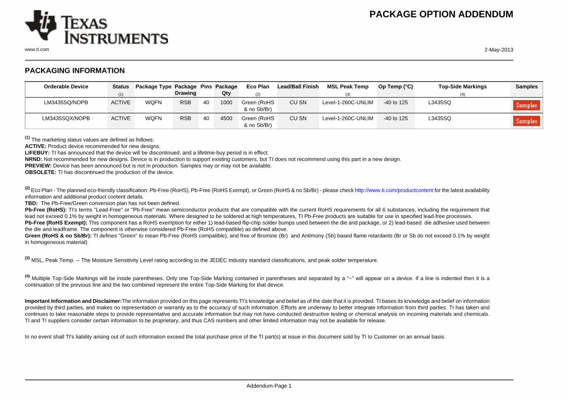
PACKAGING INFORMATION
Orderable Device Status(1)
Package Type PackageDrawing
Pins PackageQty
Eco Plan(2)
Lead/Ball Finish MSL Peak Temp(3)
Op Temp (°C) Top-Side Markings(4)
Samples
LM3435SQ/NOPB ACTIVE WQFN RSB 40 1000 Green (RoHS& no Sb/Br)
CU SN Level-1-260C-UNLIM -40 to 125 L3435SQ
LM3435SQX/NOPB ACTIVE WQFN RSB 40 4500 Green (RoHS& no Sb/Br)
CU SN Level-1-260C-UNLIM -40 to 125 L3435SQ
(1) The marketing status values are defined as follows:ACTIVE: Product device recommended for new designs.LIFEBUY: TI has announced that the device will be discontinued, and a lifetime-buy period is in effect.NRND: Not recommended for new designs. Device is in production to support existing customers, but TI does not recommend using this part in a new design.PREVIEW: Device has been announced but is not in production. Samples may or may not be available.OBSOLETE: TI has discontinued the production of the device.
(2) Eco Plan - The planned eco-friendly classification: Pb-Free (RoHS), Pb-Free (RoHS Exempt), or Green (RoHS & no Sb/Br) - please check http://www.ti.com/productcontent for the latest availabilityinformation and additional product content details.TBD: The Pb-Free/Green conversion plan has not been defined.Pb-Free (RoHS): TI's terms "Lead-Free" or "Pb-Free" mean semiconductor products that are compatible with the current RoHS requirements for all 6 substances, including the requirement thatlead not exceed 0.1% by weight in homogeneous materials. Where designed to be soldered at high temperatures, TI Pb-Free products are suitable for use in specified lead-free processes.Pb-Free (RoHS Exempt): This component has a RoHS exemption for either 1) lead-based flip-chip solder bumps used between the die and package, or 2) lead-based die adhesive used betweenthe die and leadframe. The component is otherwise considered Pb-Free (RoHS compatible) as defined above.Green (RoHS & no Sb/Br): TI defines "Green" to mean Pb-Free (RoHS compatible), and free of Bromine (Br) and Antimony (Sb) based flame retardants (Br or Sb do not exceed 0.1% by weightin homogeneous material)
(3) MSL, Peak Temp. -- The Moisture Sensitivity Level rating according to the JEDEC industry standard classifications, and peak solder temperature.
(4) Multiple Top-Side Markings will be inside parentheses. Only one Top-Side Marking contained in parentheses and separated by a "~" will appear on a device. If a line is indented then it is acontinuation of the previous line and the two combined represent the entire Top-Side Marking for that device.
Important Information and Disclaimer:The information provided on this page represents TI's knowledge and belief as of the date that it is provided. TI bases its knowledge and belief on informationprovided by third parties, and makes no representation or warranty as to the accuracy of such information. Efforts are underway to better integrate information from third parties. TI has taken andcontinues to take reasonable steps to provide representative and accurate information but may not have conducted destructive testing or chemical analysis on incoming materials and chemicals.TI and TI suppliers consider certain information to be proprietary, and thus CAS numbers and other limited information may not be available for release.
In no event shall TI's liability arising out of such information exceed the total purchase price of the TI part(s) at issue in this document sold by TI to Customer on an annual basis.
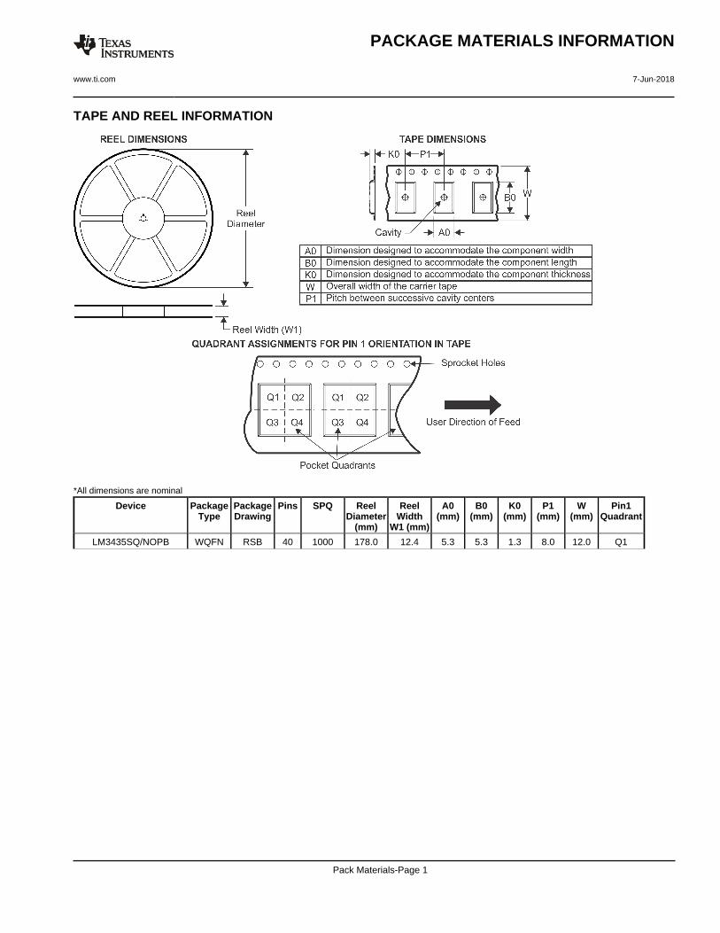
TAPE AND REEL INFORMATION
*All dimensions are nominal
Device PackageType
PackageDrawing
Pins SPQ ReelDiameter
(mm)
ReelWidth
W1 (mm)
A0(mm)
B0(mm)
K0(mm)
P1(mm)
W(mm)
Pin1Quadrant
LM3435SQ/NOPB WQFN RSB 40 1000 178.0 12.4 5.3 5.3 1.3 8.0 12.0 Q1
PACKAGE MATERIALS INFORMATION
www.ti.com 7-Jun-2018
Pack Materials-Page 1

*All dimensions are nominal
Device Package Type Package Drawing Pins SPQ Length (mm) Width (mm) Height (mm)
LM3435SQ/NOPB WQFN RSB 40 1000 210.0 185.0 35.0
PACKAGE MATERIALS INFORMATION
www.ti.com 7-Jun-2018
Pack Materials-Page 2
www.ti.com
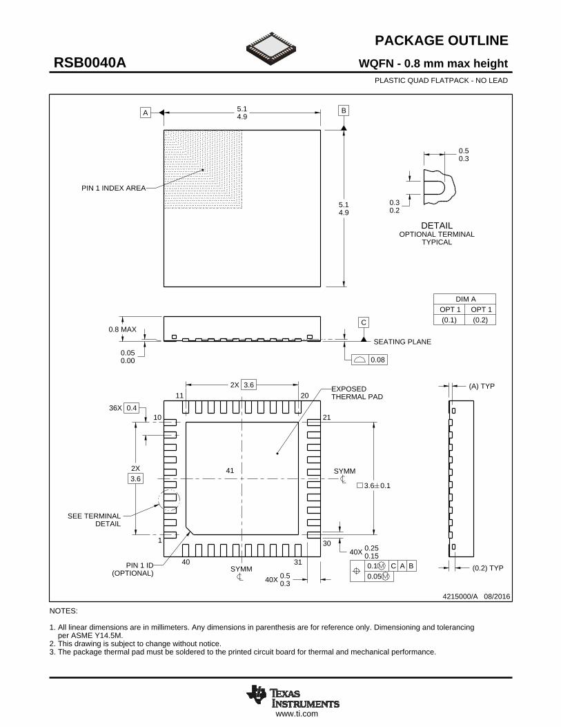
PACKAGE OUTLINE
C
SEE TERMINALDETAIL
40X 0.250.15
40X 0.50.3
0.8 MAX
(A) TYP
0.050.00
36X 0.4
2X3.6
2X 3.6
3.6 0.1
A 5.14.9
B
5.14.9
0.30.2
0.50.3
(0.2) TYP
WQFN - 0.8 mm max heightRSB0040APLASTIC QUAD FLATPACK - NO LEAD
4215000/A 08/2016
DIM A OPT 1 OPT 1(0.1) (0.2)
PIN 1 INDEX AREA
0.08
SEATING PLANE
1
10 21
30
11 20
40 31(OPTIONAL)
PIN 1 ID 0.1 C A B0.05
EXPOSEDTHERMAL PAD
41
SYMM
SYMM
NOTES: 1. All linear dimensions are in millimeters. Any dimensions in parenthesis are for reference only. Dimensioning and tolerancing per ASME Y14.5M. 2. This drawing is subject to change without notice. 3. The package thermal pad must be soldered to the printed circuit board for thermal and mechanical performance.
SCALE 2.700
DETAILOPTIONAL TERMINAL
TYPICAL
www.ti.com
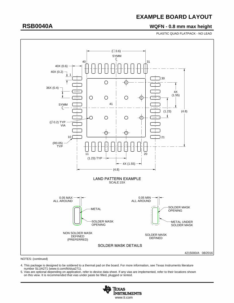
EXAMPLE BOARD LAYOUT
0.05 MINALL AROUND
0.05 MAXALL AROUND
40X (0.2)
40X (0.6)
( 0.2) TYPVIA
36X (0.4)
(4.8)
(4.8)
4X(1.55)
( 3.6)
(R0.05)TYP
(1.23)
(1.23) TYP
4X (1.55)
WQFN - 0.8 mm max heightRSB0040APLASTIC QUAD FLATPACK - NO LEAD
4215000/A 08/2016
SYMM
1
10
11 20
21
30
3140
SYMM
LAND PATTERN EXAMPLESCALE:15X
41
NOTES: (continued) 4. This package is designed to be soldered to a thermal pad on the board. For more information, see Texas Instruments literature number SLUA271 (www.ti.com/lit/slua271).5. Vias are optional depending on application, refer to device data sheet. If any vias are implemented, refer to their locations shown on this view. It is recommended that vias under paste be filled, plugged or tented.
SOLDER MASKOPENING
METAL UNDERSOLDER MASK
SOLDER MASKDEFINED
METAL
SOLDER MASKOPENING
SOLDER MASK DETAILS
NON SOLDER MASKDEFINED
(PREFERRED)
www.ti.com
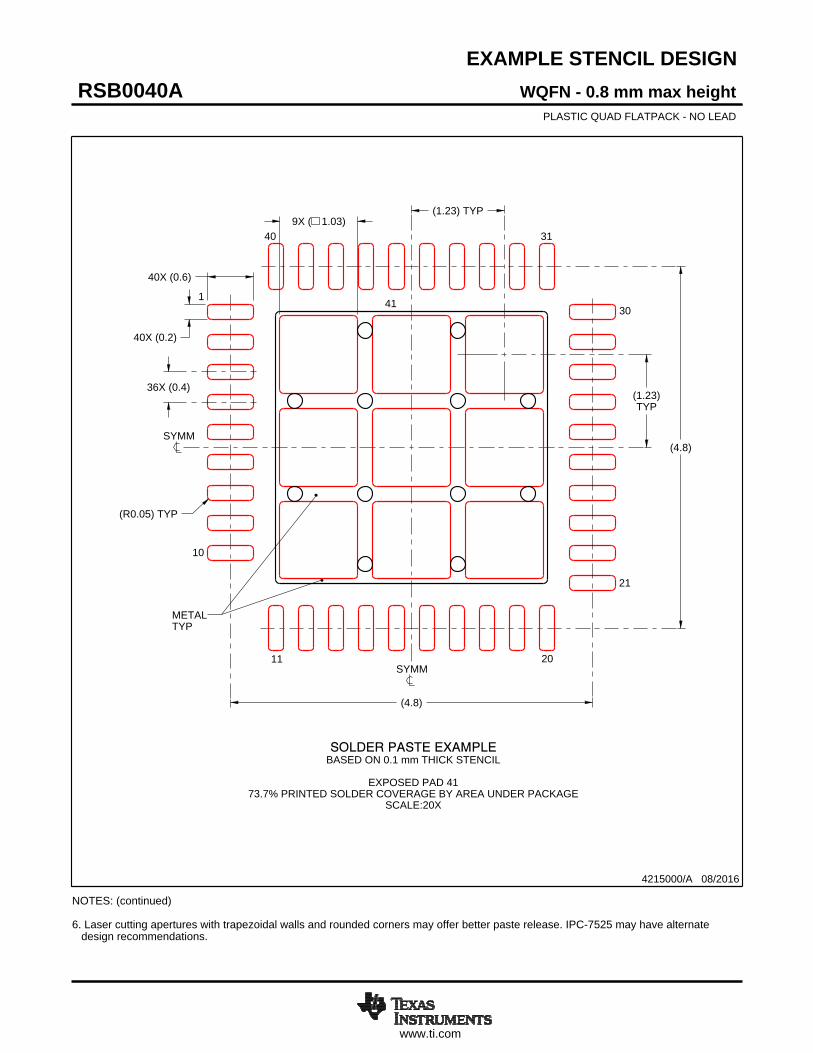
EXAMPLE STENCIL DESIGN
40X (0.6)
40X (0.2)
36X (0.4)
(4.8)
(4.8)
9X ( 1.03)
(1.23)TYP
(R0.05) TYP
(1.23) TYP
WQFN - 0.8 mm max heightRSB0040APLASTIC QUAD FLATPACK - NO LEAD
4215000/A 08/2016
NOTES: (continued) 6. Laser cutting apertures with trapezoidal walls and rounded corners may offer better paste release. IPC-7525 may have alternate design recommendations.
SYMM
METALTYP
SOLDER PASTE EXAMPLEBASED ON 0.1 mm THICK STENCIL
EXPOSED PAD 41
73.7% PRINTED SOLDER COVERAGE BY AREA UNDER PACKAGESCALE:20X
SYMM
1
10
11 20
21
30
3140
41

IMPORTANT NOTICE
Texas Instruments Incorporated (TI) reserves the right to make corrections, enhancements, improvements and other changes to itssemiconductor products and services per JESD46, latest issue, and to discontinue any product or service per JESD48, latest issue. Buyersshould obtain the latest relevant information before placing orders and should verify that such information is current and complete.TI’s published terms of sale for semiconductor products (http://www.ti.com/sc/docs/stdterms.htm) apply to the sale of packaged integratedcircuit products that TI has qualified and released to market. Additional terms may apply to the use or sale of other types of TI products andservices.Reproduction of significant portions of TI information in TI data sheets is permissible only if reproduction is without alteration and isaccompanied by all associated warranties, conditions, limitations, and notices. TI is not responsible or liable for such reproduceddocumentation. Information of third parties may be subject to additional restrictions. Resale of TI products or services with statementsdifferent from or beyond the parameters stated by TI for that product or service voids all express and any implied warranties for theassociated TI product or service and is an unfair and deceptive business practice. TI is not responsible or liable for any such statements.Buyers and others who are developing systems that incorporate TI products (collectively, “Designers”) understand and agree that Designersremain responsible for using their independent analysis, evaluation and judgment in designing their applications and that Designers havefull and exclusive responsibility to assure the safety of Designers' applications and compliance of their applications (and of all TI productsused in or for Designers’ applications) with all applicable regulations, laws and other applicable requirements. Designer represents that, withrespect to their applications, Designer has all the necessary expertise to create and implement safeguards that (1) anticipate dangerousconsequences of failures, (2) monitor failures and their consequences, and (3) lessen the likelihood of failures that might cause harm andtake appropriate actions. Designer agrees that prior to using or distributing any applications that include TI products, Designer willthoroughly test such applications and the functionality of such TI products as used in such applications.TI’s provision of technical, application or other design advice, quality characterization, reliability data or other services or information,including, but not limited to, reference designs and materials relating to evaluation modules, (collectively, “TI Resources”) are intended toassist designers who are developing applications that incorporate TI products; by downloading, accessing or using TI Resources in anyway, Designer (individually or, if Designer is acting on behalf of a company, Designer’s company) agrees to use any particular TI Resourcesolely for this purpose and subject to the terms of this Notice.TI’s provision of TI Resources does not expand or otherwise alter TI’s applicable published warranties or warranty disclaimers for TIproducts, and no additional obligations or liabilities arise from TI providing such TI Resources. TI reserves the right to make corrections,enhancements, improvements and other changes to its TI Resources. TI has not conducted any testing other than that specificallydescribed in the published documentation for a particular TI Resource.Designer is authorized to use, copy and modify any individual TI Resource only in connection with the development of applications thatinclude the TI product(s) identified in such TI Resource. NO OTHER LICENSE, EXPRESS OR IMPLIED, BY ESTOPPEL OR OTHERWISETO ANY OTHER TI INTELLECTUAL PROPERTY RIGHT, AND NO LICENSE TO ANY TECHNOLOGY OR INTELLECTUAL PROPERTYRIGHT OF TI OR ANY THIRD PARTY IS GRANTED HEREIN, including but not limited to any patent right, copyright, mask work right, orother intellectual property right relating to any combination, machine, or process in which TI products or services are used. Informationregarding or referencing third-party products or services does not constitute a license to use such products or services, or a warranty orendorsement thereof. Use of TI Resources may require a license from a third party under the patents or other intellectual property of thethird party, or a license from TI under the patents or other intellectual property of TI.TI RESOURCES ARE PROVIDED “AS IS” AND WITH ALL FAULTS. TI DISCLAIMS ALL OTHER WARRANTIES ORREPRESENTATIONS, EXPRESS OR IMPLIED, REGARDING RESOURCES OR USE THEREOF, INCLUDING BUT NOT LIMITED TOACCURACY OR COMPLETENESS, TITLE, ANY EPIDEMIC FAILURE WARRANTY AND ANY IMPLIED WARRANTIES OFMERCHANTABILITY, FITNESS FOR A PARTICULAR PURPOSE, AND NON-INFRINGEMENT OF ANY THIRD PARTY INTELLECTUALPROPERTY RIGHTS. TI SHALL NOT BE LIABLE FOR AND SHALL NOT DEFEND OR INDEMNIFY DESIGNER AGAINST ANY CLAIM,INCLUDING BUT NOT LIMITED TO ANY INFRINGEMENT CLAIM THAT RELATES TO OR IS BASED ON ANY COMBINATION OFPRODUCTS EVEN IF DESCRIBED IN TI RESOURCES OR OTHERWISE. IN NO EVENT SHALL TI BE LIABLE FOR ANY ACTUAL,DIRECT, SPECIAL, COLLATERAL, INDIRECT, PUNITIVE, INCIDENTAL, CONSEQUENTIAL OR EXEMPLARY DAMAGES INCONNECTION WITH OR ARISING OUT OF TI RESOURCES OR USE THEREOF, AND REGARDLESS OF WHETHER TI HAS BEENADVISED OF THE POSSIBILITY OF SUCH DAMAGES.Unless TI has explicitly designated an individual product as meeting the requirements of a particular industry standard (e.g., ISO/TS 16949and ISO 26262), TI is not responsible for any failure to meet such industry standard requirements.Where TI specifically promotes products as facilitating functional safety or as compliant with industry functional safety standards, suchproducts are intended to help enable customers to design and create their own applications that meet applicable functional safety standardsand requirements. Using products in an application does not by itself establish any safety features in the application. Designers mustensure compliance with safety-related requirements and standards applicable to their applications. Designer may not use any TI products inlife-critical medical equipment unless authorized officers of the parties have executed a special contract specifically governing such use.Life-critical medical equipment is medical equipment where failure of such equipment would cause serious bodily injury or death (e.g., lifesupport, pacemakers, defibrillators, heart pumps, neurostimulators, and implantables). Such equipment includes, without limitation, allmedical devices identified by the U.S. Food and Drug Administration as Class III devices and equivalent classifications outside the U.S.TI may expressly designate certain products as completing a particular qualification (e.g., Q100, Military Grade, or Enhanced Product).Designers agree that it has the necessary expertise to select the product with the appropriate qualification designation for their applicationsand that proper product selection is at Designers’ own risk. Designers are solely responsible for compliance with all legal and regulatoryrequirements in connection with such selection.Designer will fully indemnify TI and its representatives against any damages, costs, losses, and/or liabilities arising out of Designer’s non-compliance with the terms and provisions of this Notice.
Mailing Address: Texas Instruments, Post Office Box 655303, Dallas, Texas 75265Copyright © 2018, Texas Instruments Incorporated