Snva638a Layout EMI DCDC
16
Application Report SNVA638A – April 2012 – Revised April 2013 AN-2155 Layout Tips for EMI Reduction in DC / DC Converters ..................................................................................................................................................... ABSTRACT This application note will explore how the layout of your DC/DC power supply can significantly affect the amount of EMI that it produces. It will discuss several variations of a layout, analyze the results, and provide answers to some common EMI questions such whether or not to use a shielded inductor. Contents 1 Overview ..................................................................................................................... 3 2 Theory ........................................................................................................................ 3 2.1 How to Make Loop Antennas ..................................................................................... 3 2.2 Good loop antennas ............................................................................................... 3 2.3 Locating High di/dt Currents ...................................................................................... 3 2.4 How to Make Worse Antennas ................................................................................... 5 3 Setting up the Experiment ................................................................................................. 7 3.1 Layouts .............................................................................................................. 7 4 Result of Experiments ...................................................................................................... 8 5 Conclusions .................................................................................................................. 8 6 Results ....................................................................................................................... 9 6.1 EMI Results for Board Layout, tested at 12Vin, 3.3Vout and Iout = 2Amps. .............................. 9 6.2 EMI Comparisons for Board Layout ............................................................................ 11 6.3 EMI Results for Capacitor Placement ......................................................................... 12 6.4 Board 2 Gerbers and Schematic ............................................................................... 13 List of Figures 1 Current Loops ............................................................................................................... 4 2 Methods for Slowing Down the Transition Rise-Time .................................................................. 6 3 Board 1 (Control 2 Layer) .................................................................................................. 9 4 Board 2 (+GND PLANE 4 Layer) ......................................................................................... 9 5 Board 3 (- SW NODE COPPER 2 Layer)................................................................................ 9 6 Board 4 (- SW NODE COPPER 4 Layer)................................................................................ 9 7 Board 5 (Extend Switch node 2 Layer)................................................................................... 9 8 Board 6 (Extend Switch node 4 Layer)................................................................................... 9 9 Board 7 (Round Traces 2 Layer) ......................................................................................... 9 10 Board 8 (Switch node routed from top to bottom layer, 4 Layer) ..................................................... 9 11 Noise Floor ................................................................................................................. 10 12 Switching waveform for control (Board1) ............................................................................... 11 13 Switching waveform with extra ground plane (Board2)............................................................... 11 14 Switching waveform with ground plane beneath switch node cut (Board4) ....................................... 11 15 BOARD 2 vs BOARD 4 (Solid ground plane vs. ground plane beneath switch node cut) ....................... 11 16 BOARD 2 vs BOARD 6 (Original switch node length vs extended switch node length) ......................... 11 17 Placement 1 ................................................................................................................ 12 All trademarks are the property of their respective owners. 1 SNVA638A – April 2012 – Revised April 2013 AN-2155 Layout Tips for EMI Reduction in DC / DC Converters Submit Documentation Feedback Copyright © 2012–2013, Texas Instruments Incorporated
-
Upload
gregcooler123 -
Category
Documents
-
view
231 -
download
0
description
DCDC Layout
Transcript of Snva638a Layout EMI DCDC
Application ReportSNVA638A–April 2012–Revised April 2013
AN-2155 Layout Tips for EMI Reduction in DC / DCConverters
.....................................................................................................................................................
ABSTRACT
This application note will explore how the layout of your DC/DC power supply can significantly affect theamount of EMI that it produces. It will discuss several variations of a layout, analyze the results, andprovide answers to some common EMI questions such whether or not to use a shielded inductor.
Contents1 Overview ..................................................................................................................... 32 Theory ........................................................................................................................ 3
2.1 How to Make Loop Antennas ..................................................................................... 32.2 Good loop antennas ............................................................................................... 32.3 Locating High di/dt Currents ...................................................................................... 32.4 How to Make Worse Antennas ................................................................................... 5
3 Setting up the Experiment ................................................................................................. 73.1 Layouts .............................................................................................................. 7
4 Result of Experiments ...................................................................................................... 85 Conclusions .................................................................................................................. 86 Results ....................................................................................................................... 9
6.1 EMI Results for Board Layout, tested at 12Vin, 3.3Vout and Iout = 2Amps. .............................. 96.2 EMI Comparisons for Board Layout ............................................................................ 116.3 EMI Results for Capacitor Placement ......................................................................... 126.4 Board 2 Gerbers and Schematic ............................................................................... 13
List of Figures
1 Current Loops ............................................................................................................... 4
2 Methods for Slowing Down the Transition Rise-Time .................................................................. 6
3 Board 1 (Control 2 Layer).................................................................................................. 9
4 Board 2 (+GND PLANE 4 Layer) ......................................................................................... 9
5 Board 3 (- SW NODE COPPER 2 Layer)................................................................................ 9
6 Board 4 (- SW NODE COPPER 4 Layer)................................................................................ 9
7 Board 5 (Extend Switch node 2 Layer)................................................................................... 9
8 Board 6 (Extend Switch node 4 Layer)................................................................................... 9
9 Board 7 (Round Traces 2 Layer) ......................................................................................... 9
10 Board 8 (Switch node routed from top to bottom layer, 4 Layer) ..................................................... 9
11 Noise Floor ................................................................................................................. 10
12 Switching waveform for control (Board1)............................................................................... 11
13 Switching waveform with extra ground plane (Board2)............................................................... 11
14 Switching waveform with ground plane beneath switch node cut (Board4) ....................................... 11
15 BOARD 2 vs BOARD 4 (Solid ground plane vs. ground plane beneath switch node cut)....................... 11
16 BOARD 2 vs BOARD 6 (Original switch node length vs extended switch node length) ......................... 11
17 Placement 1 ................................................................................................................ 12
All trademarks are the property of their respective owners.
1SNVA638A–April 2012–Revised April 2013 AN-2155 Layout Tips for EMI Reduction in DC / DC ConvertersSubmit Documentation Feedback
Copyright © 2012–2013, Texas Instruments Incorporated
www.ti.com
18 Switching Waveform for Placement 1 .................................................................................. 12
19 EMI for Placement 1 ...................................................................................................... 12
20 Placement 2 ................................................................................................................ 12
21 Switching Waveform for Placement 2 .................................................................................. 12
22 EMI for Placement 2 ...................................................................................................... 12
23 Placement 3 ................................................................................................................ 12
24 Switching Waveform for Placement 3 .................................................................................. 12
25 EMI for Placement 3 ...................................................................................................... 12
26 Top Layer................................................................................................................... 13
27 Top Overlay ................................................................................................................ 13
28 Bottom Layer ............................................................................................................... 14
29 Bottom Overlay ............................................................................................................ 14
30 Ground Plane .............................................................................................................. 15
31 EMI Test Board Schematic * Cin1 - Cin4 are placement options ................................................... 15
2 AN-2155 Layout Tips for EMI Reduction in DC / DC Converters SNVA638A–April 2012–Revised April 2013Submit Documentation Feedback
Copyright © 2012–2013, Texas Instruments Incorporated
www.ti.com Overview
1 Overview
Electromagnetic interference (EMI) is the disruption of proper operation of an electronic device, caused byan electromagnetic field generated by a different device. To prevent electronics from interfering with theoperation of other devices, EMI is regulated by the government where the electronic device is being sold.There are several norms, for example, in the European norms (EN55022, etc.), in the USA there is FCCpart 15, in Canada there is ICES-003, in Japan there is VCCI, and so on. EMI is difficult to accuratelypredict, so the best thing you can do is to minimize the known causes of EMI when planning your layoutand design.
2 Theory
2.1 How to Make Loop Antennas
The study of EMI is really the study of antennas. So the things that make a good antenna, will alsoincrease EMI. Let's examine an electrically small loop antenna. An electrically small loop antenna is onewhere the conductor length is small compared to the wavelength of the radiating signal. As radiated EMIstandards are generally only concerned with frequencies up to 1 GHZ (which has a wavelength of 0.3meters) and a typical DC/DC converter is usually less than .075m in any given dimension, the electricallysmall loop antenna is a good starting point.E = 263 e-16 x ( f 2 x A x I ) / r Volts per meter (1)
The equation above is for the E field of differential mode EMI. We see that the radiated field is proportionalto the frequency (f) squared, the loop area (A), the current (I) and the measured distance from theradiating source to the receiving antenna (r) (1) . Frequency is in Hz, A is in m2, I is in Amps and r is inmeters. From this we can see what makes a good loop antenna.
2.2 Good loop antennas1. Radiate significantly more power for higher frequencies than for lower.
2. Radiate more power when their area is increased
3. Radiate more power when the signal current is higher
These three items play key roles in making good antennas. So to reduce EMI we need to locate all theloops in our design with high frequency currents. Then we need to decide whether we can lower thefrequency, reduce the loop area, lower the current of the signal, or some combination of all of these.
2.3 Locating High di/dt Currents
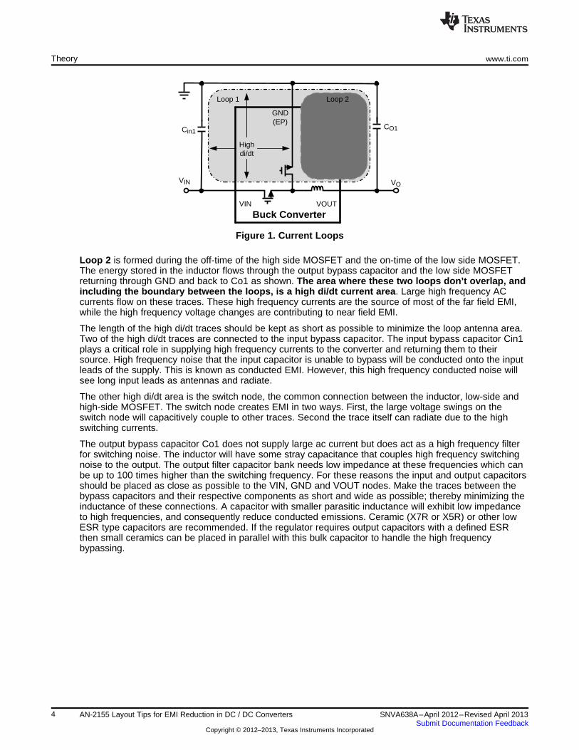
For this example, we will look at the layout of a Buck (step down) regulator. A Buck converter chops theinput voltage (VIN) into a pulse waveform at a specific duty cycle (D) such that the average voltage at theoutput of an LC filter (Vo) is D * VIN. It is important that we understand the current paths formed by theswitching action of the regulator.
In Loop 1, shown in Figure 1, current flow originates at the input bypass capacitor, Cin1 and thencontinues through the high side MOSFET during its on-time, followed by the inductor and the outputbypass capacitor Co1, finally returning to the input bypass capacitor.
(1) Henry W. Ott, "Noise Reduction Techniques In Electronics Systems", New York: Wiley- Interscience, 1988
3SNVA638A–April 2012–Revised April 2013 AN-2155 Layout Tips for EMI Reduction in DC / DC ConvertersSubmit Documentation Feedback
Copyright © 2012–2013, Texas Instruments Incorporated
VIN
GND(EP)
VIN VO
Cin1CO1
Loop 1
Buck ConverterVOUT
High di/dt
Loop 2
Theory www.ti.com
Figure 1. Current Loops
Loop 2 is formed during the off-time of the high side MOSFET and the on-time of the low side MOSFET.The energy stored in the inductor flows through the output bypass capacitor and the low side MOSFETreturning through GND and back to Co1 as shown. The area where these two loops don’t overlap, andincluding the boundary between the loops, is a high di/dt current area. Large high frequency ACcurrents flow on these traces. These high frequency currents are the source of most of the far field EMI,while the high frequency voltage changes are contributing to near field EMI.
The length of the high di/dt traces should be kept as short as possible to minimize the loop antenna area.Two of the high di/dt traces are connected to the input bypass capacitor. The input bypass capacitor Cin1plays a critical role in supplying high frequency currents to the converter and returning them to theirsource. High frequency noise that the input capacitor is unable to bypass will be conducted onto the inputleads of the supply. This is known as conducted EMI. However, this high frequency conducted noise willsee long input leads as antennas and radiate.
The other high di/dt area is the switch node, the common connection between the inductor, low-side andhigh-side MOSFET. The switch node creates EMI in two ways. First, the large voltage swings on theswitch node will capacitively couple to other traces. Second the trace itself can radiate due to the highswitching currents.
The output bypass capacitor Co1 does not supply large ac current but does act as a high frequency filterfor switching noise. The inductor will have some stray capacitance that couples high frequency switchingnoise to the output. The output filter capacitor bank needs low impedance at these frequencies which canbe up to 100 times higher than the switching frequency. For these reasons the input and output capacitorsshould be placed as close as possible to the VIN, GND and VOUT nodes. Make the traces between thebypass capacitors and their respective components as short and wide as possible; thereby minimizing theinductance of these connections. A capacitor with smaller parasitic inductance will exhibit low impedanceto high frequencies, and consequently reduce conducted emissions. Ceramic (X7R or X5R) or other lowESR type capacitors are recommended. If the regulator requires output capacitors with a defined ESRthen small ceramics can be placed in parallel with this bulk capacitor to handle the high frequencybypassing.
4 AN-2155 Layout Tips for EMI Reduction in DC / DC Converters SNVA638A–April 2012–Revised April 2013Submit Documentation Feedback
Copyright © 2012–2013, Texas Instruments Incorporated
www.ti.com Theory
2.4 How to Make Worse Antennas
The goal of our DC/DC converter design is to make bad antennas out of the loops that carry the high di/dtcurrents.
Just to re-iterate, for differential mode EMI the radiated field is proportional to the frequency (f) squared,the loop area (A), the current (I) and the measured distance from the EMI source to measurement antenna(r) (2). The distance, r, is 3 meters in our test chamber, which sets the CISPR 22 limit for frequencies below300MHz at 40dBµV/m. The radiated limits are adjusted for different test chamber sizes. For example, in a10 meter chamber the measured signal is reduced by 20 x log(10m / 3m) ≊ 10db. Thus the limit for a 10meter chamber is 10db below the limit for the 3 meter chamber.E = 263 e-16 x ( f 2 x A x I ) / r Volts per meter (2)
Let's look at an example. We have a layout with an input bypass loop area of 12 mm2. Since highfrequencies radiate more easily we will use the highest frequency of the high di/dt currents as f in ourequation. If we look at the high di/dt currents that are bypassed by the input capacitor, these switchingcurrents have a very fast rise time. We will simplify the calculation with the assumption that the highestfrequency component with significant energy (the Band Width) is equal to 0.35 divided by the rise time ofthe switch node (3) in Figure 1.f = Band Width = 0.35 / Rise Time (3)
If the measured rise time of the switch node is 10ns, then the band width is 35MHz. The current, I,associated with this frequency can be approximated by the rms input current. Which is the DC outputcurrent multiplied by the square root of the duty cycle.I = Output current x (D)1/2 (4)I = Output current x (Output Voltage / Input Voltage)1/2 (5)
For this example: the input voltage is 12 volts, the output voltage is 3.3 volts and the output current is 2amps. Thus, I = 1.05A. Therefore:E = 263 e-16 x ( (35e6Hz) 2 x 12e-6m2 x 1.05A ) / 3m
E = 135e-6 Volts / meter (6)
Are we really worrying about 135 micro volts per meter? Yes we are. The limit line for Cispr 22 Class B, at3 meters, is around 40 dBµV/m or 100 µV/m. Converting our answers into dbµV/m yields.E = 20 x log(135e-6 / 1e-6)
E = 42.6 dBµV/m (7)
So 135 µV/m puts us just over the limit line.
Our goal is to reduce this field so that we fall under the limit. We have no control over r; the distance tothe measuring antenna is determined by the regulations. What choices are left to us?
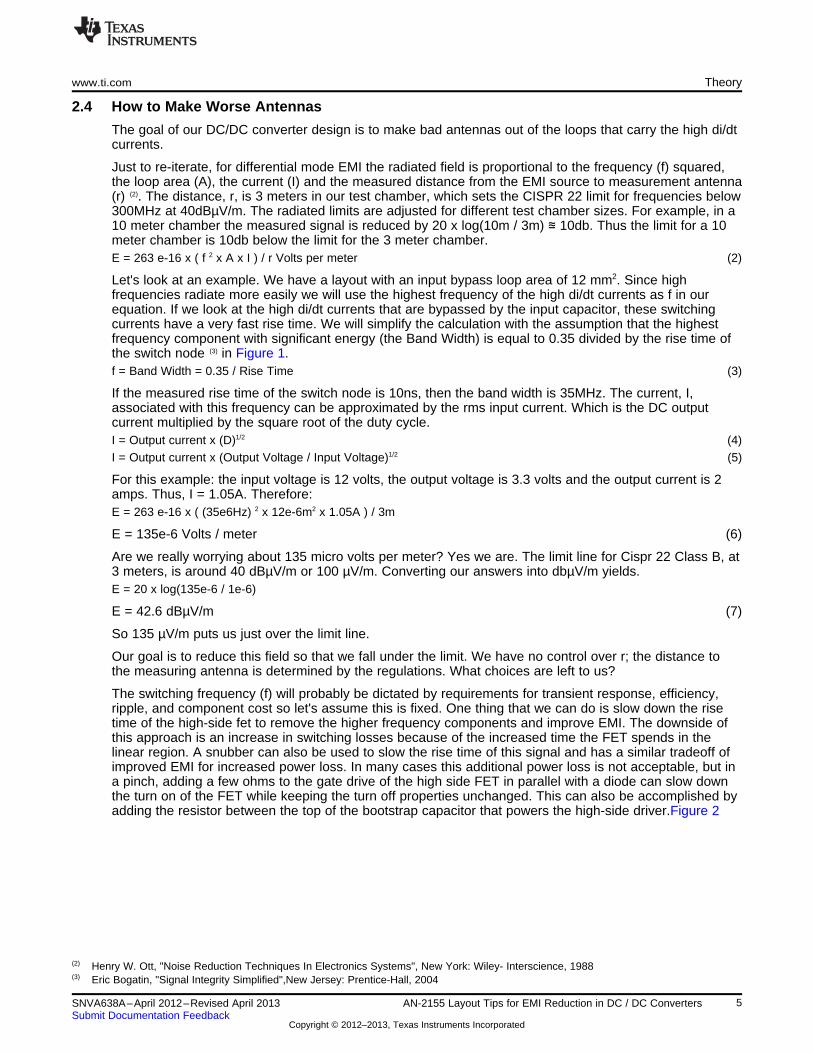
The switching frequency (f) will probably be dictated by requirements for transient response, efficiency,ripple, and component cost so let's assume this is fixed. One thing that we can do is slow down the risetime of the high-side fet to remove the higher frequency components and improve EMI. The downside ofthis approach is an increase in switching losses because of the increased time the FET spends in thelinear region. A snubber can also be used to slow the rise time of this signal and has a similar tradeoff ofimproved EMI for increased power loss. In many cases this additional power loss is not acceptable, but ina pinch, adding a few ohms to the gate drive of the high side FET in parallel with a diode can slow downthe turn on of the FET while keeping the turn off properties unchanged. This can also be accomplished byadding the resistor between the top of the bootstrap capacitor that powers the high-side driver.Figure 2
(2) Henry W. Ott, "Noise Reduction Techniques In Electronics Systems", New York: Wiley- Interscience, 1988(3) Eric Bogatin, "Signal Integrity Simplified",New Jersey: Prentice-Hall, 2004
5SNVA638A–April 2012–Revised April 2013 AN-2155 Layout Tips for EMI Reduction in DC / DC ConvertersSubmit Documentation Feedback
Copyright © 2012–2013, Texas Instruments Incorporated
3
2
L
CBST
VOUT
COUT
EP/PGND
CIN
23
VIN
1
3
Vcc
Use a resistor and diode on the gate of the high-side fet
ORA resistor in series with the bootstrap capacitor to slow down the switch transition
HSFET
LSFET
Theory www.ti.com
Figure 2. Methods for Slowing Down the Transition Rise-Time
Although we have no control over the DC input current, we can control the level of switching current thatreaches the input leads. As stated above (for a buck converter) the input bypass capacitor, Cin, isbypassing a high di/dt current. We have some control over how much of this current (I) escapes theconverter, through bypass capacitor selection and filtering. If we add an LC filter before the input capacitorwe can greatly diminish the currents on the board before they make it to longer leads or traces that canradiate. This is very useful for the input side of a buck or the output side of a boost. Note that just addingmore input capacitors can help reduce the high frequency current that reaches long input leads. This bankof capacitors should be designed such that the impedance is low up to very high frequencies. See Inputand Output Capacitor Selection Application Report SLTA055 for an example of a low impedance capacitornetwork. For guidelines on input filter design see AN-2162 Simple Success With Conducted EMI FromDC-DC Converters (SNVA489).
Finally, we have the most control over the layout and this will determine the loop area (A). When trying toreduce the loop area to design for low EMI, one of the most important things we can do is to add a groundplane. A ground plane will reduce the area of the current loops shown in Figure 1 by providing a returnpath that is a mirror image of the current path. You might ask, how does this reduce the loop area? Thecomponents are still in the same place. Doesn’t component placement define the loop area?
Think of it this way. Without the ground plane the loop area is exactly defined by the placement of thecomponents. The current must flow around the loop. If the loop is defined by a 3mm by 4mm box then thearea will be 12 mm2.
When a ground plane is added, the high frequency currents on the top layer will induce an opposingcurrent on the ground plane to cancel the magnetic field. This is often called an image current making theground plane the image plane. This return current on the ground plane reduces the area of the loop. Thinkof it by laying out the loop with a piece of rope. A second rope is placed on top of the first, with the endstied together. The loop area is now defined by twice the length of the rope multiplied by the distancebetween the ropes. The loop now has two layers and the area is now 28mm (twice the perimeter of theinitial loop) multiplied by the distance between the two layers (0.25mm for a typical PCB stack up). Theloop area is reduced to 7mm2 and a reduction in radiated energy can be achieved.
Recalculating the radiated emissions from above with the ground plane yields E= 37.94 dBµV/m acalculated improvement of 4.65 dBµV/m, and under the limit 40 dBµV/m.
6 AN-2155 Layout Tips for EMI Reduction in DC / DC Converters SNVA638A–April 2012–Revised April 2013Submit Documentation Feedback
Copyright © 2012–2013, Texas Instruments Incorporated
www.ti.com Setting up the Experiment
In summary, the primary sources of radiated noise come from the high di/dt traces. Make these tracesshort and wide enough to handle the current and bypass them effectively with a capacitor bank designedfor low impedance over a wide frequency range. Use a ground plane to decrease the area of the currentloops. If this is not enough add an LC filter to stop the high frequency currents from reaching longinput/output wires which can radiate.
3 Setting up the Experiment
With some theory in place, we can look at the effects of different layouts to test the following theories.Does a ground plane reduce EMI? Does bypass capacitor placement effect EMI? Do breaks in a groundplane effect EMI? Does rounding the edges of our traces lower EMI? ... For this experiment we took theLM3102 SIMPLE SWITCHER® Synchronous 1MHz 2.5A Step-Down Voltage Regulator (SNVS515) andcreated eight different layouts. All versions of the board are slight variations of the control board, boardnumber one. The summary below describes how the layouts differ from the control board.
3.1 Layouts1. Layout 1 is the control board, a typical layout for this particular part on a 2-layer board.
2. Two additional ground planes were added to #1 to create a four-layer board.
3. The ground copper beneath the switch node has been removed from #1.
4. The ground copper beneath the switch node has been removed from #2.
5. The length of the switch node has been doubled from #1.
6. The length of the switch node has been doubled from #2.
7. All traces were rounded to remove sharp corners from #1.
8. The switch node was routed from the top layer to the bottom layer to connect to L1 on #2.
Board number 2 was also used to test the following: a) the effect of input capacitor placement b) the effectof shielded versus non-shielded inductors, and c) the benefits of an input filter composed of L2 and Cin7.
A summary of results is shown in the following table.
7SNVA638A–April 2012–Revised April 2013 AN-2155 Layout Tips for EMI Reduction in DC / DC ConvertersSubmit Documentation Feedback
Copyright © 2012–2013, Texas Instruments Incorporated
Result of Experiments www.ti.com
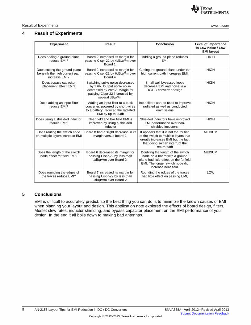
4 Result of Experiments
Experiment Result Conclusion Level of Importancein Low noise / Low
EMI layout
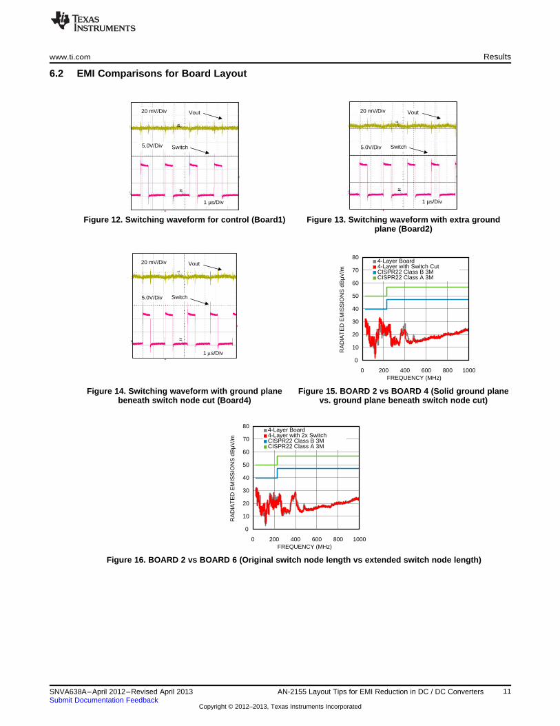
Does adding a ground plane Board 2 increased its margin for Adding a ground plane reduces HIGHreduce EMI? passing Cispr-22 by 4dBµV/m over EMI.
Board 1.
Does cutting the ground plane Board 2 increased its margin for Cutting the ground plane under the HIGHbeneath the high current path passing Cispr-22 by 6dBµV/m over high current path increases EMI.
increase EMI? Board 4.
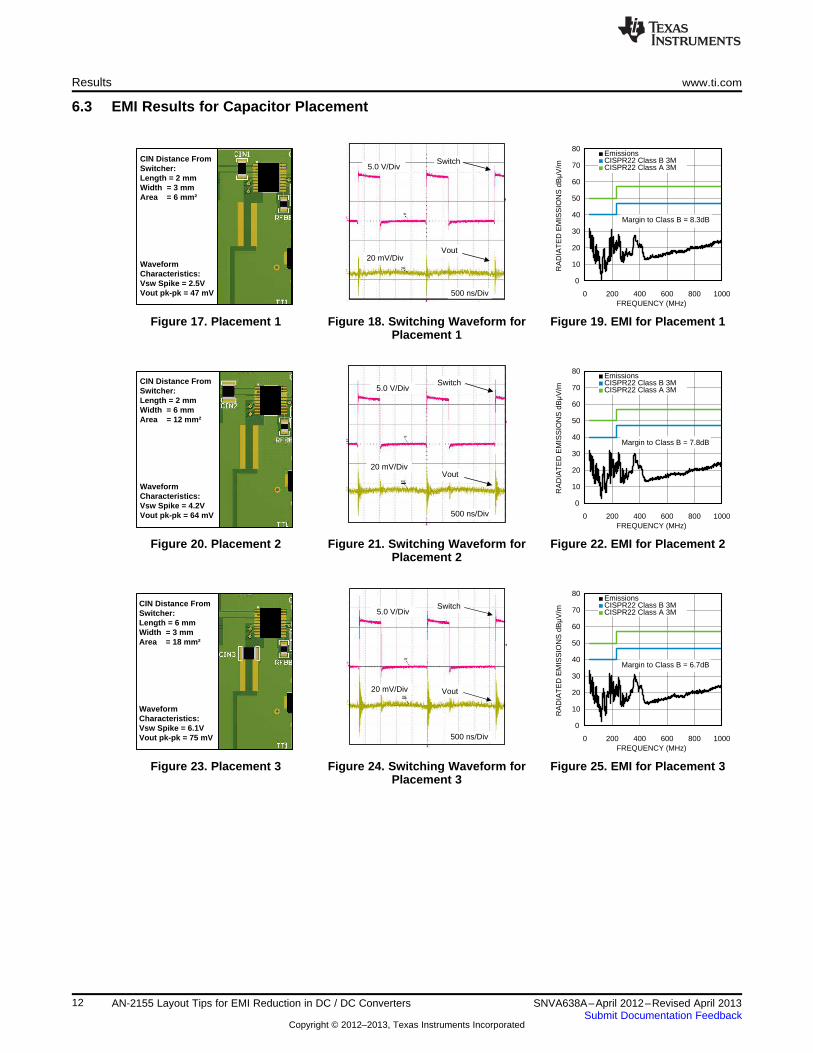
Does bypass capacitor Switching spike noise decreased Small well bypassed loops HIGHplacement affect EMI? by 3.6V. Output ripple noise decrease EMI and noise in a
decreased by 28mV. Margin for DC/DC converter design.passing Cispr-22 increased by
several dBµV/m.
Does adding an input filter Adding an input filter to a buck Input filters can be used to improve HIGHreduce EMI? converter, powered by short wires radiated as well as conducted
to a battery, reduced the radiated emmissionsEMI by up to 20db
Does using a shielded inductor Near field and Far field EMI is Shielded inductors have improved HIGHreduce EMI? improved by using a shielded EMI performance over non-
inductor shielded incuctors.
Does routing the switch node Board 8 had a slight decrease in its It appears that it is not the routing MEDIUMon multiple layers increase EMI margin versus board 2. of the switch to multiple layers that
greatly increases EMI but the factthat doing so can interrupt the
return path
Does the length of the switch Board 6 decreased its margin for Doubling the length of the switch MEDIUMnode affect far field EMI? passing Cispr-22 by less than node on a board with a ground
1dBµV/m over Board 2. plane had little effect on the farfieldEMI. The longer switch node did
increase near field.
Does rounding the edges of Board 7 increased its margin for Rounding the edges of the traces LOWthe traces reduce EMI? passing Cispr-22 by less than had little effect on passing EMI,
1dBµV/m over Board 2.
5 Conclusions
EMI is difficult to accurately predict, so the best thing you can do is to minimize the known causes of EMIwhen planning your layout and design. This application note explored the effects of board design, filters,Mosfet slew rates, inductor shielding, and bypass capacitor placement on the EMI performance of yourdesign. In the end it all boils down to making bad antennas.
8 AN-2155 Layout Tips for EMI Reduction in DC / DC Converters SNVA638A–April 2012–Revised April 2013Submit Documentation Feedback
Copyright © 2012–2013, Texas Instruments Incorporated
0 200 400 600 800 1000
0
10
20
30
40
50
60
70
80
EM
ISS
ION
S (
dB�
V/m
)
FREQUENCY (MHz)
EMISSIONSCISPR22 CLASS B 3MCISPR22 CLASS A 3M
0 200 400 600 800 1000
0
10
20
30
40
50
60
70
80
RA
DIA
TE
D E
MIS
SIO
NS
(dB�
V/m
)
FREQUENCY (MHz)
EMISSIONSCISPR22 CLASS B 3MCISPR22 CLASS A 3M
0 200 400 600 800 1000
0
10
20
30
40
50
60
70
80
EM
ISS
ION
S (
dB�
V/m
)
FREQUENCY (MHz)
EMISSIONSCISPR22 CLASS B 3MCISPR22 CLASS A 3M
0 200 400 600 800 1000
0
10
20
30
40
50
60
70
80
EM
ISS
ION
S (
dB�
V/m
)
FREQUENCY (MHz)
EMISSIONSCISPR22 CLASS B 3MCISPR22 CLASS A 3M
0 200 400 600 800 1000
0
10
20
30
40
50
60
70
80E
MIS
SIO
NS
(dB�
V/m
)
FREQUENCY (MHz)
EMISSIONSCISPR22 CLASS B 3MCISPR22 CLASS A 3M
0 200 400 600 800 1000
0
10
20
30
40
50
60
70
80
EM
ISS
ION
S (
dB�
V/m
)
FREQUENCY (MHz)
EMISSIONSCISPR22 CLASS B 3MCISPR22 CLASS A 3M
www.ti.com Results
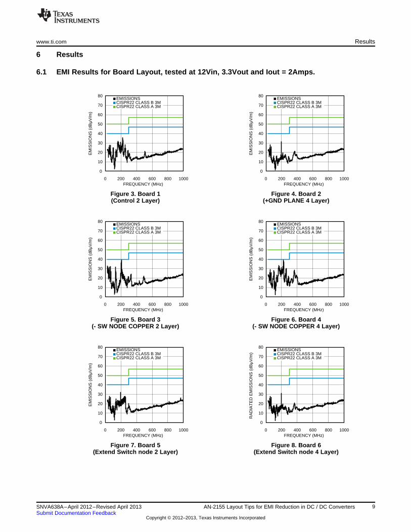
6 Results
6.1 EMI Results for Board Layout, tested at 12Vin, 3.3Vout and Iout = 2Amps.
Figure 3. Board 1 Figure 4. Board 2(Control 2 Layer) (+GND PLANE 4 Layer)
Figure 5. Board 3 Figure 6. Board 4(- SW NODE COPPER 2 Layer) (- SW NODE COPPER 4 Layer)
Figure 7. Board 5 Figure 8. Board 6(Extend Switch node 2 Layer) (Extend Switch node 4 Layer)
9SNVA638A–April 2012–Revised April 2013 AN-2155 Layout Tips for EMI Reduction in DC / DC ConvertersSubmit Documentation Feedback
Copyright © 2012–2013, Texas Instruments Incorporated
0 200 400 600 800 1000
0
10
20
30
40
50
60
70
80
RA
DIA
TE
D E
MIS
SIO
NS
(dB�
V/m
)
FREQUENCY ( MHz)
EMISSIONSCISPR22 CLASS B 3MCISPR22 CLASS A 3M
0 200 400 600 800 1000
0
10
20
30
40
50
60
70
80
RA
DIA
TE
D E
MIS
SIO
NS
(dB�
V/m
)
FREQUENCY (MHz)
EMISSIONSCISPR22 CLASS B 3MCISPR22 CLASS A 3M
0 200 400 600 800 1000
0
10
20
30
40
50
60
70
80
RA
DIA
TE
D E
MIS
SIO
NS
(dB�
V/m
)
FREQUENCY (MHz)
EMMISIONSCISPR22 CLASS B 3MCISPR22 CLASS A 3M
Results www.ti.com
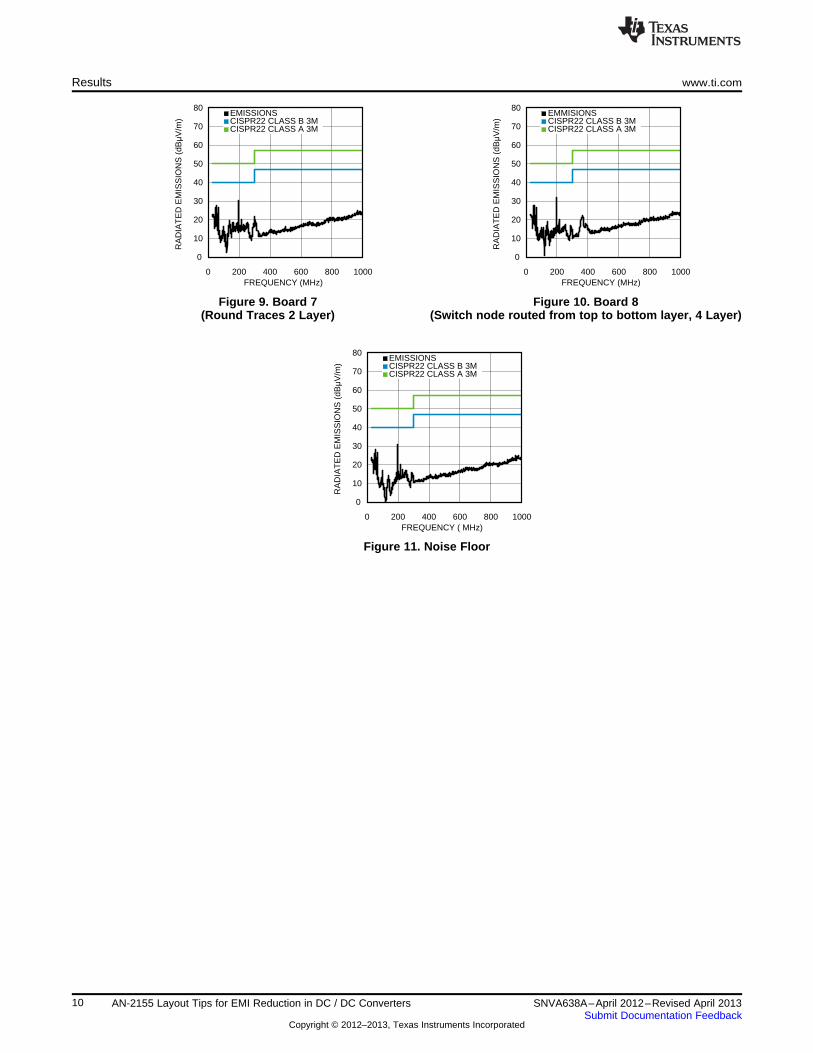
Figure 9. Board 7 Figure 10. Board 8(Round Traces 2 Layer) (Switch node routed from top to bottom layer, 4 Layer)
Figure 11. Noise Floor
10 AN-2155 Layout Tips for EMI Reduction in DC / DC Converters SNVA638A–April 2012–Revised April 2013Submit Documentation Feedback
Copyright © 2012–2013, Texas Instruments Incorporated
0 200 400 600 800 1000
0
10
20
30
40
50
60
70
80
RA
DIA
TE
D E
MIS
SIO
NS
dB�
V/m
FREQUENCY (MHz)
4-Layer Board4-Layer with 2x SwitchCISPR22 Class B 3MCISPR22 Class A 3M
0 200 400 600 800 1000
0
10
20
30
40
50
60
70
80
RA
DIA
TE
D E
MIS
SIO
NS
dB�
V/m
FREQUENCY (MHz)
4-Layer Board4-Layer with Switch CutCISPR22 Class B 3MCISPR22 Class A 3M
1 Ps/Div
Switch
20 mV/Div
5.0V/Div
Vout
1 µs/Div
Switch
20 mV/Div
5.0V/Div
Vout
1 µs/Div
Switch
20 mV/Div
5.0V/Div
Vout
www.ti.com Results
6.2 EMI Comparisons for Board Layout
Figure 12. Switching waveform for control (Board1) Figure 13. Switching waveform with extra groundplane (Board2)
Figure 14. Switching waveform with ground plane Figure 15. BOARD 2 vs BOARD 4 (Solid ground planebeneath switch node cut (Board4) vs. ground plane beneath switch node cut)
Figure 16. BOARD 2 vs BOARD 6 (Original switch node length vs extended switch node length)
11SNVA638A–April 2012–Revised April 2013 AN-2155 Layout Tips for EMI Reduction in DC / DC ConvertersSubmit Documentation Feedback
Copyright © 2012–2013, Texas Instruments Incorporated
0 200 400 600 800 1000
0
10
20
30
40
50
60
70
80
RA
DIA
TE
D E
MIS
SIO
NS
dB�
V/m
FREQUENCY (MHz)
Margin to Class B = 6.7dB
EmissionsCISPR22 Class B 3MCISPR22 Class A 3M
CIN Distance From Switcher:Length = 6 mmWidth = 3 mmArea = 18 mm²
Waveform Characteristics:Vsw Spike = 6.1VVout pk-pk = 75 mV 500 ns/Div
Switch
20 mV/Div
5.0 V/Div
Vout
0 200 400 600 800 1000
0
10
20
30
40
50
60
70
80
RA
DIA
TE
D E
MIS
SIO
NS
dB�
V/m
FREQUENCY (MHz)
Margin to Class B = 7.8dB
EmissionsCISPR22 Class B 3MCISPR22 Class A 3M
CIN Distance From Switcher:Length = 2 mmWidth = 6 mmArea = 12 mm²
Waveform Characteristics:Vsw Spike = 4.2VVout pk-pk = 64 mV 500 ns/Div
Switch
20 mV/Div
5.0 V/Div
Vout
0 200 400 600 800 1000
0
10
20
30
40
50
60
70
80
RA
DIA
TE
D E
MIS
SIO
NS
dB�
V/m
FREQUENCY (MHz)
Margin to Class B = 8.3dB
EmissionsCISPR22 Class B 3MCISPR22 Class A 3M
CIN Distance From Switcher:Length = 2 mmWidth = 3 mmArea = 6 mm²
Waveform Characteristics:Vsw Spike = 2.5VVout pk-pk = 47 mV 500 ns/Div
Switch
20 mV/Div
5.0 V/Div
Vout
Results www.ti.com
6.3 EMI Results for Capacitor Placement
Figure 17. Placement 1 Figure 18. Switching Waveform for Figure 19. EMI for Placement 1Placement 1
Figure 20. Placement 2 Figure 21. Switching Waveform for Figure 22. EMI for Placement 2Placement 2
Figure 23. Placement 3 Figure 24. Switching Waveform for Figure 25. EMI for Placement 3Placement 3
12 AN-2155 Layout Tips for EMI Reduction in DC / DC Converters SNVA638A–April 2012–Revised April 2013Submit Documentation Feedback
Copyright © 2012–2013, Texas Instruments Incorporated
www.ti.com Results
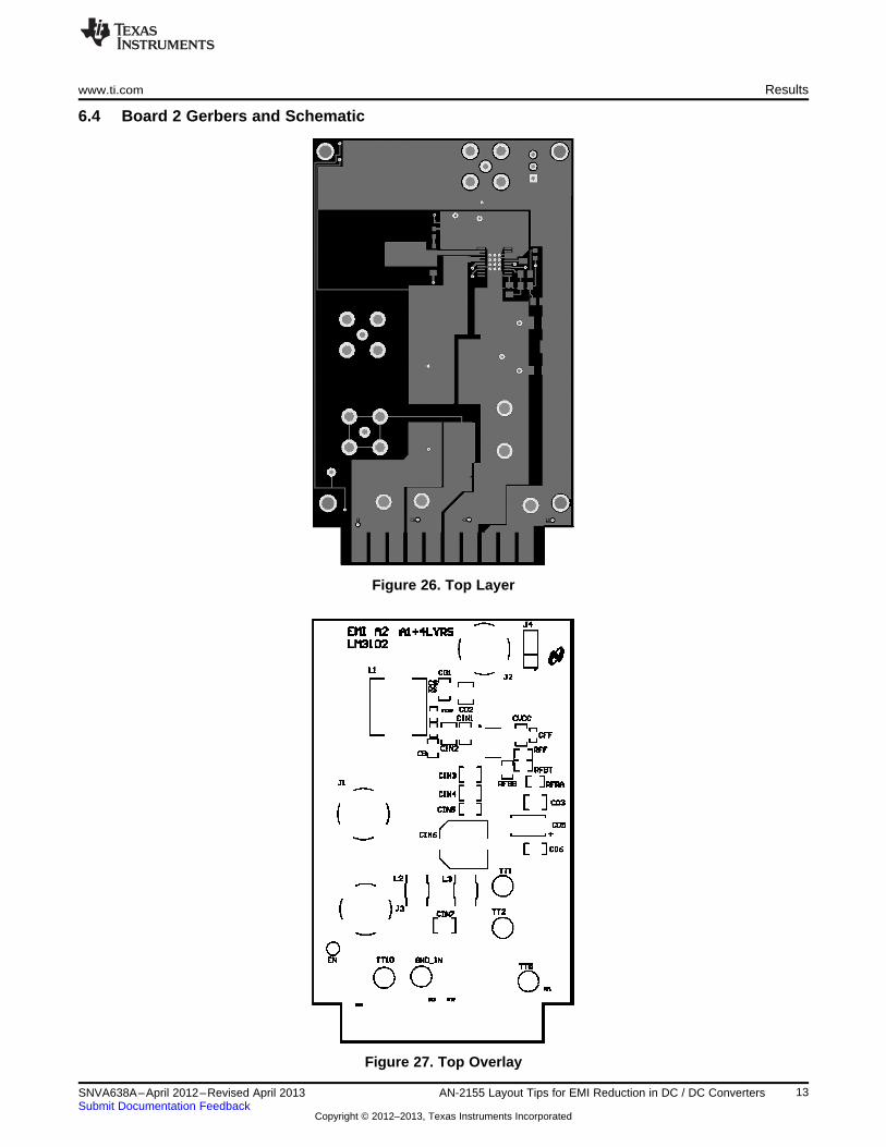
6.4 Board 2 Gerbers and Schematic
Figure 26. Top Layer
Figure 27. Top Overlay
13SNVA638A–April 2012–Revised April 2013 AN-2155 Layout Tips for EMI Reduction in DC / DC ConvertersSubmit Documentation Feedback
Copyright © 2012–2013, Texas Instruments Incorporated
Results www.ti.com
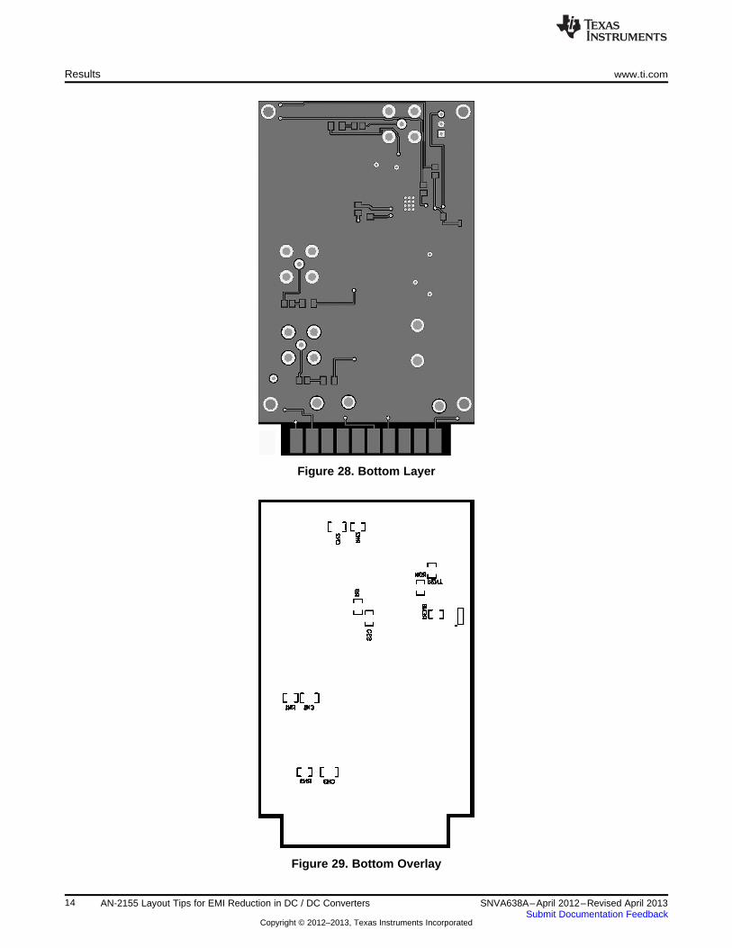
Figure 28. Bottom Layer
Figure 29. Bottom Overlay
14 AN-2155 Layout Tips for EMI Reduction in DC / DC Converters SNVA638A–April 2012–Revised April 2013Submit Documentation Feedback
Copyright © 2012–2013, Texas Instruments Incorporated
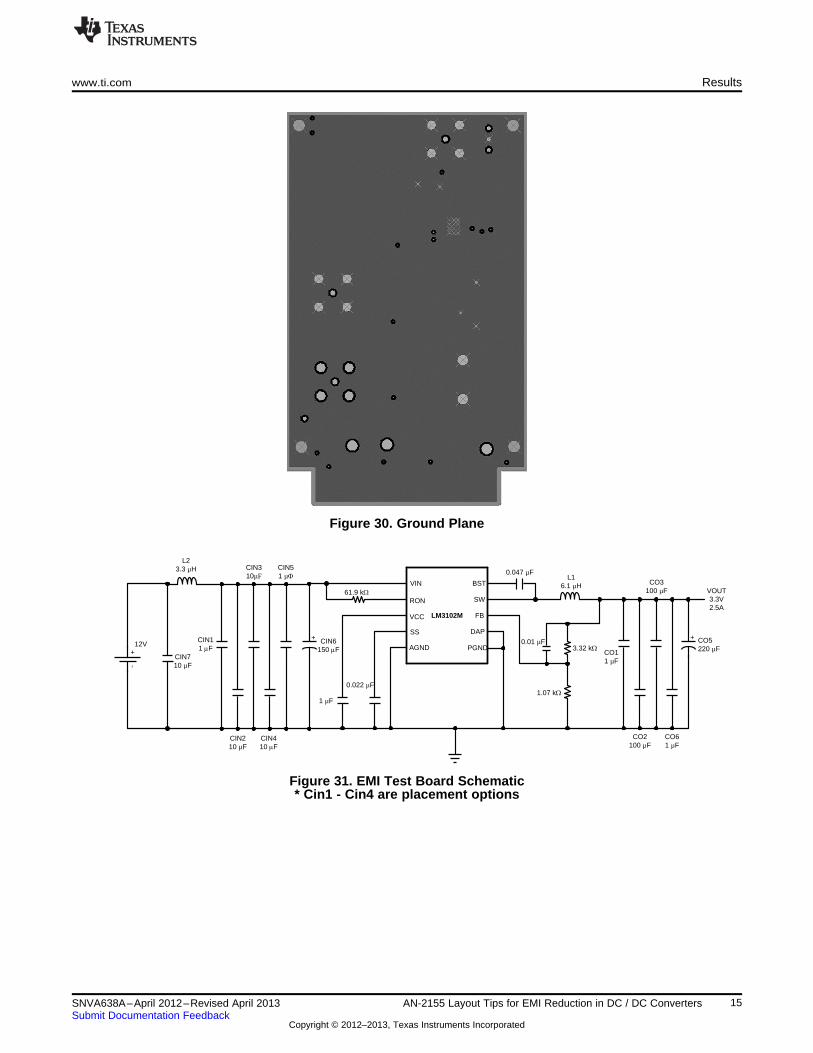
VIN
RON
VCC
SS
AGND PGND
DAP
FB
SW
BST
LM3102M
VOUT3.3V2.5A
+ +
61.9 k:
1 µF
0.022 µF
3.32 k:
1.07 k:
0.01 µF
0.047 µF
CIN11 PF
CIN210 µF
CIN310µF
CIN410 PF
CIN51 µ)
CIN6150 PF
CIN710 µF
CO11 µF
CO2100 µF
CO3100 µF
CO61 µF
CO5220 µF
L23.3 µH
L16.1 µH
-+ 12V
www.ti.com Results
Figure 30. Ground Plane
Figure 31. EMI Test Board Schematic* Cin1 - Cin4 are placement options
15SNVA638A–April 2012–Revised April 2013 AN-2155 Layout Tips for EMI Reduction in DC / DC ConvertersSubmit Documentation Feedback
Copyright © 2012–2013, Texas Instruments Incorporated

IMPORTANT NOTICE
Texas Instruments Incorporated and its subsidiaries (TI) reserve the right to make corrections, enhancements, improvements and otherchanges to its semiconductor products and services per JESD46, latest issue, and to discontinue any product or service per JESD48, latestissue. Buyers should obtain the latest relevant information before placing orders and should verify that such information is current andcomplete. All semiconductor products (also referred to herein as “components”) are sold subject to TI’s terms and conditions of salesupplied at the time of order acknowledgment.
TI warrants performance of its components to the specifications applicable at the time of sale, in accordance with the warranty in TI’s termsand conditions of sale of semiconductor products. Testing and other quality control techniques are used to the extent TI deems necessaryto support this warranty. Except where mandated by applicable law, testing of all parameters of each component is not necessarilyperformed.
TI assumes no liability for applications assistance or the design of Buyers’ products. Buyers are responsible for their products andapplications using TI components. To minimize the risks associated with Buyers’ products and applications, Buyers should provideadequate design and operating safeguards.
TI does not warrant or represent that any license, either express or implied, is granted under any patent right, copyright, mask work right, orother intellectual property right relating to any combination, machine, or process in which TI components or services are used. Informationpublished by TI regarding third-party products or services does not constitute a license to use such products or services or a warranty orendorsement thereof. Use of such information may require a license from a third party under the patents or other intellectual property of thethird party, or a license from TI under the patents or other intellectual property of TI.
Reproduction of significant portions of TI information in TI data books or data sheets is permissible only if reproduction is without alterationand is accompanied by all associated warranties, conditions, limitations, and notices. TI is not responsible or liable for such altereddocumentation. Information of third parties may be subject to additional restrictions.
Resale of TI components or services with statements different from or beyond the parameters stated by TI for that component or servicevoids all express and any implied warranties for the associated TI component or service and is an unfair and deceptive business practice.TI is not responsible or liable for any such statements.
Buyer acknowledges and agrees that it is solely responsible for compliance with all legal, regulatory and safety-related requirementsconcerning its products, and any use of TI components in its applications, notwithstanding any applications-related information or supportthat may be provided by TI. Buyer represents and agrees that it has all the necessary expertise to create and implement safeguards whichanticipate dangerous consequences of failures, monitor failures and their consequences, lessen the likelihood of failures that might causeharm and take appropriate remedial actions. Buyer will fully indemnify TI and its representatives against any damages arising out of the useof any TI components in safety-critical applications.
In some cases, TI components may be promoted specifically to facilitate safety-related applications. With such components, TI’s goal is tohelp enable customers to design and create their own end-product solutions that meet applicable functional safety standards andrequirements. Nonetheless, such components are subject to these terms.
No TI components are authorized for use in FDA Class III (or similar life-critical medical equipment) unless authorized officers of the partieshave executed a special agreement specifically governing such use.
Only those TI components which TI has specifically designated as military grade or “enhanced plastic” are designed and intended for use inmilitary/aerospace applications or environments. Buyer acknowledges and agrees that any military or aerospace use of TI componentswhich have not been so designated is solely at the Buyer's risk, and that Buyer is solely responsible for compliance with all legal andregulatory requirements in connection with such use.
TI has specifically designated certain components as meeting ISO/TS16949 requirements, mainly for automotive use. In any case of use ofnon-designated products, TI will not be responsible for any failure to meet ISO/TS16949.
Products Applications
Audio www.ti.com/audio Automotive and Transportation www.ti.com/automotive
Amplifiers amplifier.ti.com Communications and Telecom www.ti.com/communications
Data Converters dataconverter.ti.com Computers and Peripherals www.ti.com/computers
DLP® Products www.dlp.com Consumer Electronics www.ti.com/consumer-apps
DSP dsp.ti.com Energy and Lighting www.ti.com/energy
Clocks and Timers www.ti.com/clocks Industrial www.ti.com/industrial
Interface interface.ti.com Medical www.ti.com/medical
Logic logic.ti.com Security www.ti.com/security
Power Mgmt power.ti.com Space, Avionics and Defense www.ti.com/space-avionics-defense
Microcontrollers microcontroller.ti.com Video and Imaging www.ti.com/video
RFID www.ti-rfid.com
OMAP Applications Processors www.ti.com/omap TI E2E Community e2e.ti.com
Wireless Connectivity www.ti.com/wirelessconnectivity
Mailing Address: Texas Instruments, Post Office Box 655303, Dallas, Texas 75265Copyright © 2013, Texas Instruments Incorporated