SN74ALVCH16823 18-BITBUS-INTERFACEFLIP-FLOP WITH 3 ...
24
www.ti.com FEATURES DESCRIPTION DGG OR DL PACKAGE (TOP VIEW) 1 2 3 4 5 6 7 8 9 10 11 12 13 14 15 16 17 18 19 20 21 22 23 24 25 26 27 28 56 55 54 53 52 51 50 49 48 47 46 45 44 43 42 41 40 39 38 37 36 35 34 33 32 31 30 29 1CLR 1OE 1Q1 GND 1Q2 1Q3 V CC 1Q4 1Q5 1Q6 GND 1Q7 1Q8 1Q9 2Q1 2Q2 2Q3 GND 2Q4 2Q5 2Q6 V CC 2Q7 2Q8 GND 2Q9 2OE 2CLR 1CLK 1CLKEN 1D1 GND 1D2 1D3 V CC 1D4 1D5 1D6 GND 1D7 1D8 1D9 2D1 2D2 2D3 GND 2D4 2D5 2D6 V CC 2D7 2D8 GND 2D9 2CLKEN 2CLK A buffered output-enable (OE) input can be used to place the nine outputs in either a normal logic state (high or SN74ALVCH16823 18-BIT BUS-INTERFACE FLIP-FLOP WITH 3-STATE OUTPUTS SCES038F – JULY 1995 – REVISED APRIL 2005 • Member of the Texas Instruments Widebus™ Family • EPIC™ (Enhanced-Performance Implanted CMOS) Submicron Process • ESD Protection Exceeds 2000 V Per MIL-STD-883, Method 3015; Exceeds 200 V Using Machine Model (C = 200 pF, R = 0) • Latch-Up Performance Exceeds 250 mA Per JESD 17 • Bus Hold on Data Inputs Eliminates the Need for External Pullup/Pulldown Resistors • Package Options Include Plastic 300-mil Shrink Small-Outline (DL) and Thin Shrink Small-Outline (DGG) Packages This 18-bit bus-interface flip-flop is designed for 1.65-V to 3.6-V V CC operation. The SN74ALVCH16823 features 3-state outputs designed specifically for driving highly capacitive or relatively low-impedance loads. This device is particularly suitable for implementing wider buffer registers, I/O ports, bidirectional bus drivers with parity, and working registers. The SN74ALVCH16823 can be used as two 9-bit flip-flops or one 18-bit flip-flop. With the clock-enable (CLKEN) input low, the D-type flip-flops enter data on the low-to-high transitions of the clock. Taking CLKEN high disables the clock buffer, thus latching the outputs. Taking the clear (CLR) input low causes the Q outputs to go low independently of the clock. low logic levels) or the high-impedance state. In the high-impedance state, the outputs neither load nor drive the bus lines significantly. The high-impedance state and increased drive provide the capability to drive bus lines without need for interface or pullup components. The output-enable (OE) input does not affect the internal operation of the flip-flops. Old data can be retained or new data can be entered while the outputs are in the high-impedance state. To ensure the high-impedance state during power up or power down, OE should be tied to V CC through a pullup resistor; the minimum value of the resistor is determined by the current-sinking capability of the driver. Active bus-hold circuitry is provided to hold unused or floating data inputs at a valid logic level. The SN74ALVCH16823 is characterized for operation from –40°C to 85°C. Please be aware that an important notice concerning availability, standard warranty, and use in critical applications of Texas Instruments semiconductor products and disclaimers thereto appears at the end of this data sheet. Widebus, EPIC are trademarks of Texas Instruments. PRODUCTION DATA information is current as of publication date. Copyright © 1995–2005, Texas Instruments Incorporated Products conform to specifications per the terms of the Texas Instruments standard warranty. Production processing does not necessarily include testing of all parameters.
Transcript of SN74ALVCH16823 18-BITBUS-INTERFACEFLIP-FLOP WITH 3 ...

www.ti.com
FEATURES
DESCRIPTION
DGG OR DL PACKAGE(TOP VIEW)
1
2
3
4
5
6
7
8
9
10
11
12
13
14
15
16
17
18
19
20
21
22
23
24
25
26
27
28
56
55
54
53
52
51
50
49
48
47
46
45
44
43
42
41
40
39
38
37
36
35
34
33
32
31
30
29
1CLR1OE1Q1
GND1Q21Q3VCC
1Q41Q51Q6
GND1Q71Q81Q92Q12Q22Q3
GND2Q42Q52Q6VCC2Q72Q8
GND2Q92OE
2CLR
1CLK1CLKEN1D1GND1D21D3VCC
1D41D51D6GND1D71D81D92D12D22D3GND2D42D52D6VCC2D72D8GND2D92CLKEN2CLK
A buffered output-enable (OE) input can be used to place the nine outputs in either a normal logic state (high or
SN74ALVCH1682318-BIT BUS-INTERFACE FLIP-FLOP
WITH 3-STATE OUTPUTSSCES038F–JULY 1995–REVISED APRIL 2005
• Member of the Texas Instruments Widebus™Family
• EPIC™ (Enhanced-Performance ImplantedCMOS) Submicron Process
• ESD Protection Exceeds 2000 V PerMIL-STD-883, Method 3015; Exceeds 200 VUsing Machine Model (C = 200 pF, R = 0)
• Latch-Up Performance Exceeds 250 mA PerJESD 17
• Bus Hold on Data Inputs Eliminates the Needfor External Pullup/Pulldown Resistors
• Package Options Include Plastic 300-milShrink Small-Outline (DL) and Thin ShrinkSmall-Outline (DGG) Packages
This 18-bit bus-interface flip-flop is designed for1.65-V to 3.6-V VCC operation.
The SN74ALVCH16823 features 3-state outputsdesigned specifically for driving highly capacitive orrelatively low-impedance loads. This device isparticularly suitable for implementing wider bufferregisters, I/O ports, bidirectional bus drivers withparity, and working registers.
The SN74ALVCH16823 can be used as two 9-bitflip-flops or one 18-bit flip-flop. With the clock-enable(CLKEN) input low, the D-type flip-flops enter data onthe low-to-high transitions of the clock. TakingCLKEN high disables the clock buffer, thus latchingthe outputs. Taking the clear (CLR) input low causesthe Q outputs to go low independently of the clock.
low logic levels) or the high-impedance state. In the high-impedance state, the outputs neither load nor drive thebus lines significantly. The high-impedance state and increased drive provide the capability to drive bus lineswithout need for interface or pullup components.
The output-enable (OE) input does not affect the internal operation of the flip-flops. Old data can be retained ornew data can be entered while the outputs are in the high-impedance state.
To ensure the high-impedance state during power up or power down, OE should be tied to VCC through a pullupresistor; the minimum value of the resistor is determined by the current-sinking capability of the driver.
Active bus-hold circuitry is provided to hold unused or floating data inputs at a valid logic level.
The SN74ALVCH16823 is characterized for operation from –40°C to 85°C.
Please be aware that an important notice concerning availability, standard warranty, and use in critical applications of TexasInstruments semiconductor products and disclaimers thereto appears at the end of this data sheet.
Widebus, EPIC are trademarks of Texas Instruments.
PRODUCTION DATA information is current as of publication date. Copyright © 1995–2005, Texas Instruments IncorporatedProducts conform to specifications per the terms of the TexasInstruments standard warranty. Production processing does notnecessarily include testing of all parameters.
www.ti.com
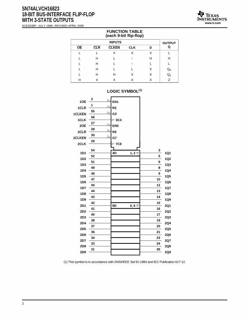
(1) This symbol is in accordance with ANSI/IEEE Std 91-1984 and IEC Publication 617-12.
EN12
561CLK 3C4
4D54
1D1 1Q13
521D2 1Q2
5
511D3 1Q3
6
491D4 1Q4
8
481D5 1Q5
9
471D6 1Q6
10
451D7 1Q7
12
441D8 1Q8
13
431D9 1Q9
14
1, 2
8D42
2D1 2Q115
412D2 2Q2
16
402D3 2Q3
17
382D4 2Q4
19
372D5 2Q5
20
362D6 2Q6
21
342D7 2Q7
23
332D8 2Q8
24
312D9 2Q9
26
5, 6
R21
G355
EN527
292CLK 7C8
R628
G730
1OE
1CLR
1CLKEN
2OE
2CLR
2CLKEN
SN74ALVCH1682318-BIT BUS-INTERFACE FLIP-FLOPWITH 3-STATE OUTPUTSSCES038F–JULY 1995–REVISED APRIL 2005
FUNCTION TABLE(each 9-bit flip-flop)
INPUTS OUTPUTQOE CLR CLKEN CLK D
L L X X X L
L H L ↑ H H
L H L ↑ L L
L H L L X Q0
L H H X X Q0
H X X X X Z
LOGIC SYMBOL(1)
2

www.ti.com
To Eight Other Channels
1D1
1Q1
1CLKEN
1OE
1CLR
2
1
55
54
R
1D
C13
CE
561CLK
To Eight Other Channels
2D1
2Q1
2CLKEN
2OE
2CLR
27
28
30
42
R
1D
C115
CE
292CLK
Absolute Maximum Ratings (1)
SN74ALVCH1682318-BIT BUS-INTERFACE FLIP-FLOP
WITH 3-STATE OUTPUTSSCES038F–JULY 1995–REVISED APRIL 2005
LOGIC DIAGRAM (POSITIVE LOGIC)
over operating free-air temperature range (unless otherwise noted)
MIN MAX UNIT
VCC Supply voltage range –0.5 4.6 V
VI Input voltage range (2) –0.5 4.6 V
VO Output voltage range (2) (3) –0.5 VCC + 0.5 V
IIK Input clamp current VI < 0 –50 mA
IOK Output clamp current VO < 0 –50 mA
IO Continuous output current ±50 mA
Continuous current through VCC or GND ±100 mA
DGG package 81θJA Package thermal impedance (4) °C/W
DL package 74
Tstg Storage temperature range –65 150 °C
(1) Stresses beyond those listed under "absolute maximum ratings" may cause permanent damage to the device. These are stress ratingsonly, and functional operation of the device at these or any other conditions beyond those indicated under "recommended operatingconditions" is not implied. Exposure to absolute-maximum-rated conditions for extended periods may affect device reliability.
(2) The input negative-voltage and output voltage ratings may be exceeded if the input and output current ratings are observed.(3) This value is limited to 4.6 V maximum.(4) The package thermal impedance is calculated in accordance with JESD 51.
3

www.ti.com
Recommended Operating Conditions (1)
SN74ALVCH1682318-BIT BUS-INTERFACE FLIP-FLOPWITH 3-STATE OUTPUTSSCES038F–JULY 1995–REVISED APRIL 2005
MIN MAX UNIT
VCC Supply voltage 1.65 3.6 V
VCC = 1.65 V to 1.95 V 0.65 × VCC
VIH High-level input voltage VCC = 2.3 V to 2.7 V 1.7 V
VCC = 2.7 V to 3.6 V 2
VCC = 1.65 V to 1.95 V 0.35 × VCC
VIL Low-level input voltage VCC = 2.3 V to 2.7 V 0.7 V
VCC = 2.7 V to 3.6 V 0.8
VI Input voltage 0 VCC V
VO Output voltage 0 VCC V
VCC = 1.65 V –4
VCC = 2.3 V –12IOH High-level output current mA
VCC = 2.7 V –12
VCC = 3 V –24
VCC = 1.65 V 4
VCC = 2.3 V 12IOL Low-level output current mA
VCC = 2.7 V 12
VCC = 3 V 24
∆t/∆v Input transition rise or fall rate 10 ns/V
TA Operating free-air temperature –40 85 °C
(1) All unused control inputs of the device must be held at VCC or GND to ensure proper device operation. Refer to the TI application report,Implications of Slow or Floating CMOS Inputs, literature number SCBA004.
4

www.ti.com
Electrical Characteristics
SN74ALVCH1682318-BIT BUS-INTERFACE FLIP-FLOP
WITH 3-STATE OUTPUTSSCES038F–JULY 1995–REVISED APRIL 2005
over recommended operating free-air temperature range (unless otherwise noted)
PARAMETER TEST CONDITIONS VCC MIN TYP (1) MAX UNIT
VCC –IOH = –100 µA 1.65 V to 3.6 V 0.2
IOH = –4 mA 1.65 V 1.2
IOH = –6 mA 2.3 V 2VOH V2.3 V 1.7
IOH = –12 mA 2.7 V 2.2
3 V 2.4
IOH = –24 mA 3 V 2
IOL = 100 µA 1.65 V to 3.6 V 0.2
IOL = 4 mA 1.65 V 0.45
IOL = 6 mA 2.3 V 0.4VOL V
2.3 V 0.7IOL = 12 mA
2.7 V 0.4
IOL = 24 mA 3 V 0.55
II VI = VCC or GND 3.6 V ±5 µA
VI = 0.58 V 1.65 V 25
VI = 1.07 V 1.65 V –25
VI = 0.7 V 2.3 V 45
II(hold) VI = 1.7 V 2.3 V –45 µA
VI = 0.8 V 3 V 75
VI = 2 V 3 V –75
VI = 0 to 3.6 V (2) 3.6 V ±500
IOZ VO = VCC or GND 3.6 V ±10 µA
ICC VI = VCC or GND, IO = 0 3.6 V 40 µA
∆ICC One input at VCC – 0.6 V, Other inputs at VCC or GND 3 V to 3.6 V 750 µA
Control inputs 4.5Ci VI = VCC or GND 3.3 V pF
Data inputs 6.5
Co Outputs VO = VCC or GND 3.3 V 7 pF
(1) All typical values are at VCC = 3.3 V, TA = 25°C.(2) This is the bus-hold maximum dynamic current. It is the minimum overdrive current required to switch the input from one state to
another.
5
www.ti.com
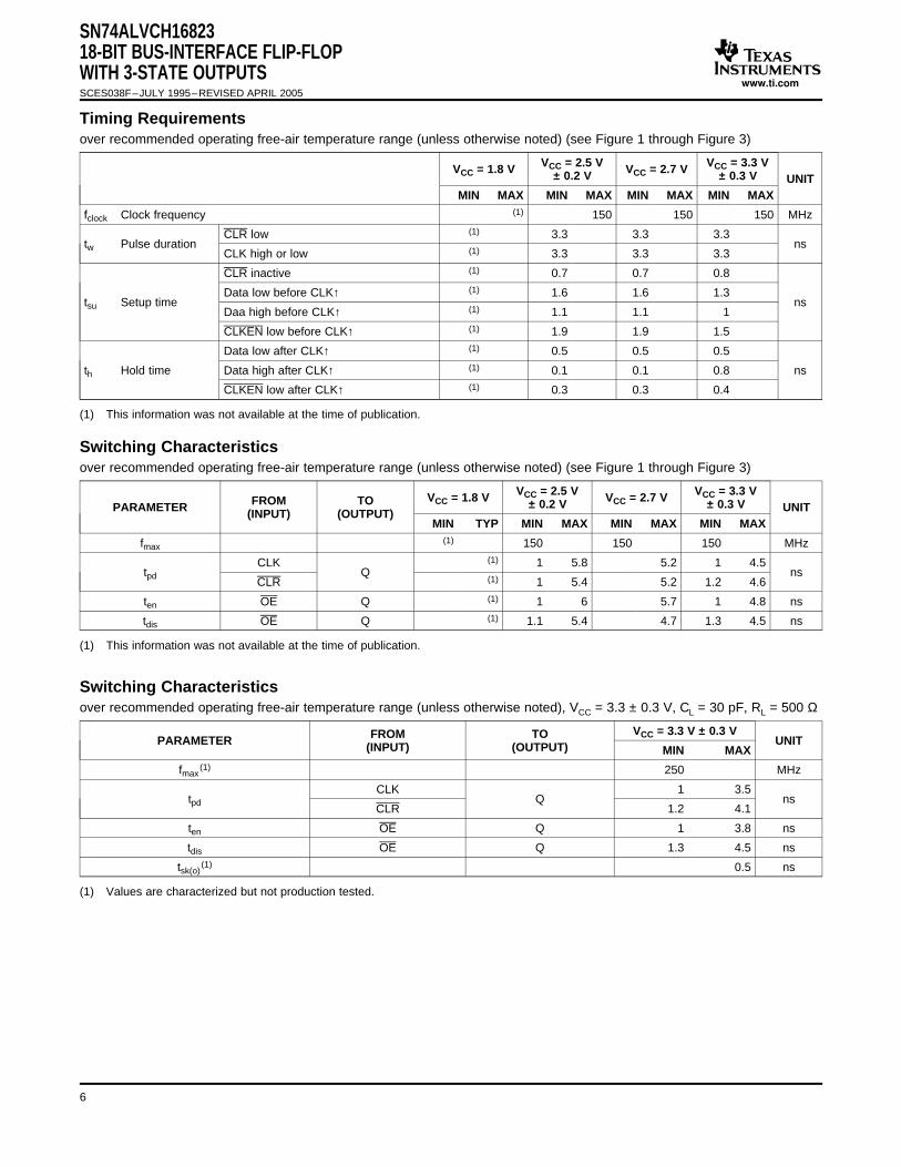
Timing Requirements
Switching Characteristics
Switching Characteristics
SN74ALVCH1682318-BIT BUS-INTERFACE FLIP-FLOPWITH 3-STATE OUTPUTSSCES038F–JULY 1995–REVISED APRIL 2005
over recommended operating free-air temperature range (unless otherwise noted) (see Figure 1 through Figure 3)
VCC = 2.5 V VCC = 3.3 VVCC = 1.8 V VCC = 2.7 V± 0.2 V ± 0.3 V UNITMIN MAX MIN MAX MIN MAX MIN MAX
fclock Clock frequency (1) 150 150 150 MHz
CLR low (1) 3.3 3.3 3.3tw Pulse duration ns
CLK high or low (1) 3.3 3.3 3.3
CLR inactive (1) 0.7 0.7 0.8
Data low before CLK↑ (1) 1.6 1.6 1.3tsu Setup time ns
Daa high before CLK↑ (1) 1.1 1.1 1
CLKEN low before CLK↑ (1) 1.9 1.9 1.5
Data low after CLK↑ (1) 0.5 0.5 0.5
th Hold time Data high after CLK↑ (1) 0.1 0.1 0.8 ns
CLKEN low after CLK↑ (1) 0.3 0.3 0.4
(1) This information was not available at the time of publication.
over recommended operating free-air temperature range (unless otherwise noted) (see Figure 1 through Figure 3)
VCC = 2.5 V VCC = 3.3 VVCC = 1.8 V VCC = 2.7 VFROM TO ± 0.2 V ± 0.3 VPARAMETER UNIT(INPUT) (OUTPUT)MIN TYP MIN MAX MIN MAX MIN MAX
fmax(1) 150 150 150 MHz
CLK (1) 1 5.8 5.2 1 4.5tpd Q ns
CLR (1) 1 5.4 5.2 1.2 4.6
ten OE Q (1) 1 6 5.7 1 4.8 ns
tdis OE Q (1) 1.1 5.4 4.7 1.3 4.5 ns
(1) This information was not available at the time of publication.
over recommended operating free-air temperature range (unless otherwise noted), VCC = 3.3 ± 0.3 V, CL = 30 pF, RL = 500 Ω
VCC = 3.3 V ± 0.3 VFROM TOPARAMETER UNIT(INPUT) (OUTPUT) MIN MAX
fmax(1) 250 MHz
CLK 1 3.5tpd Q ns
CLR 1.2 4.1
ten OE Q 1 3.8 ns
tdis OE Q 1.3 4.5 ns
tsk(o)(1) 0.5 ns
(1) Values are characterized but not production tested.
6

www.ti.com
Operating Characteristics
SN74ALVCH1682318-BIT BUS-INTERFACE FLIP-FLOP
WITH 3-STATE OUTPUTSSCES038F–JULY 1995–REVISED APRIL 2005
TA = 25°C
VCC = 1.8 V VCC = 2.5 V VCC = 3.3 VTESTPARAMETER UNITCONDITIONS TYP TYP TYP
Outputs enabled (1) 27 30Power dissipationCpd CL = 50 pF, f = 10 MHz pFcapacitance Outputs disabled (1) 16 18
(1) This information was not available at the time of publication.
7

www.ti.com
PARAMETER MEASUREMENT INFORMATION
VCC/2
VCC/2
VCC/2VCC/2
VCC/2VCC/2
VCC/2VCC/2
VOH
VOL
thtsu
From OutputUnder Test
CL = 30 pF(see Note A)
LOAD CIRCUIT
S1 Open
GND
1 kΩ
1 kΩ
OutputControl
(low-levelenabling)
OutputWaveform 1
S1 at 2 × VCC(see Note B)
OutputWaveform 2
S1 at GND(see Note B)
tPZL
tPZH
tPLZ
tPHZ
0 V
VOL + 0.15 V
VOH − 0.15 V
0 V
VCC
0 V
0 V
tw
VCCVCC
VOLTAGE WAVEFORMSSETUP AND HOLD TIMES
VOLTAGE WAVEFORMSPULSE DURATION
VOLTAGE WAVEFORMSENABLE AND DISABLE TIMES
TimingInput
DataInput
Input
tpdtPLZ/tPZLtPHZ/tPZH
Open2 × VCC
GND
TEST S1
NOTES: A. CL includes probe and jig capacitance.B. Waveform 1 is for an output with internal conditions such that the output is low, except when disabled by the output control.
Waveform 2 is for an output with internal conditions such that the output is high, except when disabled by the output control.C. All input pulses are supplied by generators having the following characteristics: PRR ≤ 10 MHz, ZO = 50 Ω, tr ≤ 2 ns, tf ≤ 2 ns.D. The outputs are measured one at a time, with one transition per measurement.E. tPLZ and tPHZ are the same as tdis.F. tPZL and tPZH are the same as ten.G. tPLH and tPHL are the same as tpd.
0 V
VCC
VCC/2
tPHL
VCC/2 VCC/2VCC
0 V
VOH
VOL
Input
Output
VOLTAGE WAVEFORMSPROPAGATION DELAY TIMES
VCC/2 VCC/2
tPLH
2 × VCC
VCC
SN74ALVCH1682318-BIT BUS-INTERFACE FLIP-FLOPWITH 3-STATE OUTPUTSSCES038F–JULY 1995–REVISED APRIL 2005
VCC = 1.8 V
Figure 1. Load Circuit and Voltage Waveforms
8

www.ti.com
PARAMETER MEASUREMENT INFORMATION
VCC/2
VCC/2
VCC/2VCC/2
VCC/2VCC/2
VCC/2VCC/2
VOH
VOL
thtsu
From OutputUnder Test
CL = 30 pF(see Note A)
LOAD CIRCUIT
S1 Open
GND
500 Ω
500 Ω
OutputControl
(low-levelenabling)
OutputWaveform 1
S1 at 2 × VCC(see Note B)
OutputWaveform 2
S1 at GND(see Note B)
tPZL
tPZH
tPLZ
tPHZ
0 V
VOL + 0.15 V
VOH − 0.15 V
0 V
VCC
0 V
0 V
tw
VCCVCC
VOLTAGE WAVEFORMSSETUP AND HOLD TIMES
VOLTAGE WAVEFORMSPULSE DURATION
VOLTAGE WAVEFORMSENABLE AND DISABLE TIMES
TimingInput
DataInput
Input
tpdtPLZ/tPZLtPHZ/tPZH
Open2 × VCC
GND
TEST S1
NOTES: A. CL includes probe and jig capacitance.B. Waveform 1 is for an output with internal conditions such that the output is low, except when disabled by the output control.
Waveform 2 is for an output with internal conditions such that the output is high, except when disabled by the output control.C. All input pulses are supplied by generators having the following characteristics: PRR ≤ 10 MHz, ZO = 50 Ω, tr ≤ 2 ns, tf ≤ 2 ns.D. The outputs are measured one at a time, with one transition per measurement.E. tPLZ and tPHZ are the same as tdis.F. tPZL and tPZH are the same as ten.G. tPLH and tPHL are the same as tpd.
0 V
VCC
VCC/2
tPHL
VCC/2 VCC/2VCC
0 V
VOH
VOL
Input
Output
VOLTAGE WAVEFORMSPROPAGATION DELAY TIMES
VCC/2 VCC/2
tPLH
2 × VCC
VCC
SN74ALVCH1682318-BIT BUS-INTERFACE FLIP-FLOP
WITH 3-STATE OUTPUTSSCES038F–JULY 1995–REVISED APRIL 2005
VCC = 2.5 V ± 0.2 V
Figure 2. Load Circuit and Voltage Waveforms
9

www.ti.com
PARAMETER MEASUREMENT INFORMATION
VOH
VOL
thtsu
From Output Under Test
CL = 50 pF(see Note A)
LOAD CIRCUIT
S16 V
Open
GND
500 Ω
500 Ω
tPLH tPHL
OutputControl
(low-levelenabling)
OutputWaveform 1
S1 at 6 V(see Note B)
OutputWaveform 2
S1 at GND(see Note B)
tPZL
tPZH
tPLZ
tPHZ
1.5 V 1.5 V2.7 V
0 V
1.5 V 1.5 VVOH
VOL
0 V
1.5 V VOL + 0.3 V
1.5 VVOH − 0.3 V
0 V
1.5 V2.7 V
0 V
1.5 V
2.7 V
0 V
1.5 V 1.5 V
tw
Input
3 V
VOLTAGE WAVEFORMSSETUP AND HOLD TIMES
VOLTAGE WAVEFORMSPROPAGATION DELAY TIMES
VOLTAGE WAVEFORMSPULSE DURATION
VOLTAGE WAVEFORMSENABLE AND DISABLE TIMES
TimingInput
DataInput
Output
Input
tpdtPLZ/tPZLtPHZ/tPZH
Open6 V
GND
TEST S1
NOTES: A. CL includes probe and jig capacitance.B. Waveform 1 is for an output with internal conditions such that the output is low, except when disabled by the output control.
Waveform 2 is for an output with internal conditions such that the output is high, except when disabled by the output control.C. All input pulses are supplied by generators having the following characteristics: PRR ≤ 10 MHz, ZO = 50 Ω, tr ≤ 2.5 ns, tf ≤ 2.5 ns.D. The outputs are measured one at a time, with one transition per measurement.E. tPLZ and tPHZ are the same as tdis.F. tPZL and tPZH are the same as ten.G. tPLH and tPHL are the same as tpd.
1.5 V2.7 V
0 V
2.7 V
1.5 V1.5 V
SN74ALVCH1682318-BIT BUS-INTERFACE FLIP-FLOPWITH 3-STATE OUTPUTSSCES038F–JULY 1995–REVISED APRIL 2005
VCC = 2.7 V AND 3.3 V ± 0.3 V
Figure 3. Load Circuit and Voltage Waveforms
10

PACKAGE OPTION ADDENDUM
www.ti.com 10-Dec-2020
Addendum-Page 1
PACKAGING INFORMATION
Orderable Device Status(1)
Package Type PackageDrawing
Pins PackageQty
Eco Plan(2)
Lead finish/Ball material
(6)
MSL Peak Temp(3)
Op Temp (°C) Device Marking(4/5)
Samples
SN74ALVCH16823DGGR ACTIVE TSSOP DGG 56 2000 RoHS & Green NIPDAU Level-1-260C-UNLIM -40 to 85 ALVCH16823
SN74ALVCH16823DGVR ACTIVE TVSOP DGV 56 2000 RoHS & Green NIPDAU Level-1-260C-UNLIM -40 to 85 VH823
SN74ALVCH16823DL ACTIVE SSOP DL 56 20 RoHS & Green NIPDAU Level-1-260C-UNLIM -40 to 85 ALVCH16823
SN74ALVCH16823DLR ACTIVE SSOP DL 56 1000 RoHS & Green NIPDAU Level-1-260C-UNLIM -40 to 85 ALVCH16823
(1) The marketing status values are defined as follows:ACTIVE: Product device recommended for new designs.LIFEBUY: TI has announced that the device will be discontinued, and a lifetime-buy period is in effect.NRND: Not recommended for new designs. Device is in production to support existing customers, but TI does not recommend using this part in a new design.PREVIEW: Device has been announced but is not in production. Samples may or may not be available.OBSOLETE: TI has discontinued the production of the device.
(2) RoHS: TI defines "RoHS" to mean semiconductor products that are compliant with the current EU RoHS requirements for all 10 RoHS substances, including the requirement that RoHS substancedo not exceed 0.1% by weight in homogeneous materials. Where designed to be soldered at high temperatures, "RoHS" products are suitable for use in specified lead-free processes. TI mayreference these types of products as "Pb-Free".RoHS Exempt: TI defines "RoHS Exempt" to mean products that contain lead but are compliant with EU RoHS pursuant to a specific EU RoHS exemption.Green: TI defines "Green" to mean the content of Chlorine (Cl) and Bromine (Br) based flame retardants meet JS709B low halogen requirements of <=1000ppm threshold. Antimony trioxide basedflame retardants must also meet the <=1000ppm threshold requirement.
(3) MSL, Peak Temp. - The Moisture Sensitivity Level rating according to the JEDEC industry standard classifications, and peak solder temperature.
(4) There may be additional marking, which relates to the logo, the lot trace code information, or the environmental category on the device.
(5) Multiple Device Markings will be inside parentheses. Only one Device Marking contained in parentheses and separated by a "~" will appear on a device. If a line is indented then it is a continuationof the previous line and the two combined represent the entire Device Marking for that device.
(6) Lead finish/Ball material - Orderable Devices may have multiple material finish options. Finish options are separated by a vertical ruled line. Lead finish/Ball material values may wrap to twolines if the finish value exceeds the maximum column width.
Important Information and Disclaimer:The information provided on this page represents TI's knowledge and belief as of the date that it is provided. TI bases its knowledge and belief on informationprovided by third parties, and makes no representation or warranty as to the accuracy of such information. Efforts are underway to better integrate information from third parties. TI has taken and

PACKAGE OPTION ADDENDUM
www.ti.com 10-Dec-2020
Addendum-Page 2
continues to take reasonable steps to provide representative and accurate information but may not have conducted destructive testing or chemical analysis on incoming materials and chemicals.TI and TI suppliers consider certain information to be proprietary, and thus CAS numbers and other limited information may not be available for release.
In no event shall TI's liability arising out of such information exceed the total purchase price of the TI part(s) at issue in this document sold by TI to Customer on an annual basis.

TAPE AND REEL INFORMATION
*All dimensions are nominal
Device PackageType
PackageDrawing
Pins SPQ ReelDiameter
(mm)
ReelWidth
W1 (mm)
A0(mm)
B0(mm)
K0(mm)
P1(mm)
W(mm)
Pin1Quadrant
SN74ALVCH16823DGGR TSSOP DGG 56 2000 330.0 24.4 8.6 15.6 1.8 12.0 24.0 Q1
SN74ALVCH16823DGVR TVSOP DGV 56 2000 330.0 24.4 6.8 11.7 1.6 12.0 24.0 Q1
SN74ALVCH16823DLR SSOP DL 56 1000 330.0 32.4 11.35 18.67 3.1 16.0 32.0 Q1
PACKAGE MATERIALS INFORMATION
www.ti.com 5-Jan-2022
Pack Materials-Page 1

*All dimensions are nominal
Device Package Type Package Drawing Pins SPQ Length (mm) Width (mm) Height (mm)
SN74ALVCH16823DGGR TSSOP DGG 56 2000 367.0 367.0 45.0
SN74ALVCH16823DGVR TVSOP DGV 56 2000 367.0 367.0 45.0
SN74ALVCH16823DLR SSOP DL 56 1000 367.0 367.0 55.0
PACKAGE MATERIALS INFORMATION
www.ti.com 5-Jan-2022
Pack Materials-Page 2

TUBE
*All dimensions are nominal
Device Package Name Package Type Pins SPQ L (mm) W (mm) T (µm) B (mm)
SN74ALVCH16823DL DL SSOP 56 20 473.7 14.24 5110 7.87
PACKAGE MATERIALS INFORMATION
www.ti.com 5-Jan-2022
Pack Materials-Page 3

MECHANICAL DATA
MPDS006C – FEBRUARY 1996 – REVISED AUGUST 2000
POST OFFICE BOX 655303 • DALLAS, TEXAS 75265
DGV (R-PDSO-G**) PLASTIC SMALL-OUTLINE 24 PINS SHOWN
14
3,70
3,50 4,90
5,10
20DIM
PINS **
4073251/E 08/00
1,20 MAX
Seating Plane
0,050,15
0,25
0,500,75
0,230,13
1 12
24 13
4,304,50
0,16 NOM
Gage Plane
A
7,90
7,70
382416
4,90
5,103,70
3,50
A MAX
A MIN
6,606,20
11,20
11,40
56
9,60
9,80
48
0,08
M0,070,40
0°–8°
NOTES: A. All linear dimensions are in millimeters.B. This drawing is subject to change without notice.C. Body dimensions do not include mold flash or protrusion, not to exceed 0,15 per side.D. Falls within JEDEC: 24/48 Pins – MO-153
14/16/20/56 Pins – MO-194

www.ti.com
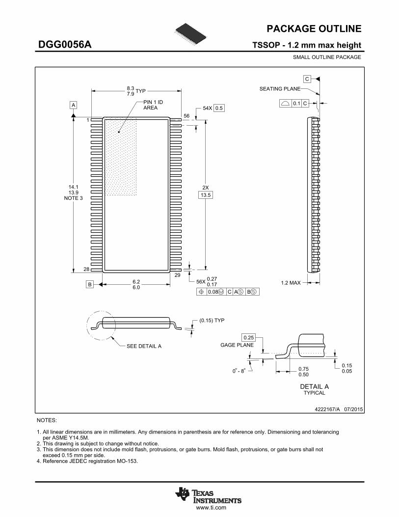
PACKAGE OUTLINE
C
54X 0.4
2X10.8
56X 0.230.13
6.66.2 TYP
SEATINGPLANE
0.150.05
0.25GAGE PLANE
0 -8
1.21.1
B 4.54.3
NOTE 4
A
11.411.2
NOTE 3
0.750.50
(0.15) TYP
TVSOP - 1.2 mm max heightDGV0056ASMALL OUTLINE PACKAGE
4220240/B 12/2020
1
2829
56
0.1 C A B
PIN 1 INDEXAREA
SEE DETAIL A
0.08 C
NOTES: 1. All linear dimensions are in millimeters. Any dimensions in parenthesis are for reference only. Dimensioning and tolerancing per ASME Y14.5M. 2. This drawing is subject to change without notice. 3. This dimension does not include mold flash, protrusions, or gate burrs. Mold flash, protrusions, or gate burrs shall not exceed 0.15 mm per side. 4. This dimension does not include interlead flash. Interlead flash shall not exceed 0.25 mm per side.5. Reference JEDEC registration MO-194.
A 15DETAIL ATYPICAL
SCALE 1.500

www.ti.com
EXAMPLE BOARD LAYOUT
0.05 MAXALL AROUND
0.05 MINALL AROUND
56X(1.4)
56X (0.2)
54X (0.4)
(5.9)
(R0.05) TYP
TVSOP - 1.2 mm max heightDGV0056ASMALL OUTLINE PACKAGE
4220240/B 12/2020
NOTES: (continued) 6. Publication IPC-7351 may have alternate designs. 7. Solder mask tolerances between and around signal pads can vary based on board fabrication site.
LAND PATTERN EXAMPLEEXPOSED METAL SHOWN
SCALE: 8X
SYMM
SYMM
1
28 29
56
15.000
METAL EDGESOLDER MASKOPENING
METAL UNDERSOLDER MASK
SOLDER MASKOPENING
EXPOSED METALEXPOSED METAL
SOLDER MASK DETAILS
NON-SOLDER MASKDEFINED
(PREFERRED)
SOLDER MASKDEFINED

www.ti.com
EXAMPLE STENCIL DESIGN
56X(1.4)
56X (0.2)
54X (0.4)
(5.9)
(R0.05) TYP
TVSOP - 1.2 mm max heightDGV0056ASMALL OUTLINE PACKAGE
4220240/B 12/2020
NOTES: (continued) 8. Laser cutting apertures with trapezoidal walls and rounded corners may offer better paste release. IPC-7525 may have alternate design recommendations. 9. Board assembly site may have different recommendations for stencil design.
SOLDER PASTE EXAMPLEBASED ON 0.125 mm THICK STENCIL
SCALE: 8X
SYMM
SYMM
1
28 29
56

www.ti.com
PACKAGE OUTLINE
C
TYP8.37.9
1.2 MAX
54X 0.5
56X 0.270.17
2X13.5
(0.15) TYP
0 - 80.150.05
0.25GAGE PLANE
0.750.50
A
NOTE 3
14.113.9
B 6.26.0
4222167/A 07/2015
TSSOP - 1.2 mm max heightDGG0056ASMALL OUTLINE PACKAGE
NOTES: 1. All linear dimensions are in millimeters. Any dimensions in parenthesis are for reference only. Dimensioning and tolerancing per ASME Y14.5M. 2. This drawing is subject to change without notice. 3. This dimension does not include mold flash, protrusions, or gate burrs. Mold flash, protrusions, or gate burrs shall not exceed 0.15 mm per side.4. Reference JEDEC registration MO-153.
156
0.08 C A B
2928
PIN 1 IDAREA
SEATING PLANE
0.1 C
SEE DETAIL A
DETAIL ATYPICAL
SCALE 1.200

www.ti.com
EXAMPLE BOARD LAYOUT
(7.5)
0.05 MAXALL AROUND
0.05 MINALL AROUND
56X (1.5)
56X (0.3)
54X (0.5)
(R )TYP
0.05
4222167/A 07/2015
TSSOP - 1.2 mm max heightDGG0056ASMALL OUTLINE PACKAGE
SYMM
SYMM
LAND PATTERN EXAMPLESCALE:6X
1
28 29
56
NOTES: (continued) 5. Publication IPC-7351 may have alternate designs. 6. Solder mask tolerances between and around signal pads can vary based on board fabrication site.
METALSOLDER MASKOPENING
NON SOLDER MASKDEFINED
SOLDER MASK DETAILS
SOLDER MASKOPENING
METAL UNDERSOLDER MASK
SOLDER MASKDEFINED

www.ti.com
EXAMPLE STENCIL DESIGN
(7.5)
54X (0.5)
56X (0.3)
56X (1.5)
(R ) TYP0.05
4222167/A 07/2015
TSSOP - 1.2 mm max heightDGG0056ASMALL OUTLINE PACKAGE
NOTES: (continued) 7. Laser cutting apertures with trapezoidal walls and rounded corners may offer better paste release. IPC-7525 may have alternate design recommendations. 8. Board assembly site may have different recommendations for stencil design.
SYMM
SYMM
1
28 29
56
SOLDER PASTE EXAMPLEBASED ON 0.125 mm THICK STENCIL
SCALE:6X

IMPORTANT NOTICE AND DISCLAIMERTI PROVIDES TECHNICAL AND RELIABILITY DATA (INCLUDING DATA SHEETS), DESIGN RESOURCES (INCLUDING REFERENCE DESIGNS), APPLICATION OR OTHER DESIGN ADVICE, WEB TOOLS, SAFETY INFORMATION, AND OTHER RESOURCES “AS IS” AND WITH ALL FAULTS, AND DISCLAIMS ALL WARRANTIES, EXPRESS AND IMPLIED, INCLUDING WITHOUT LIMITATION ANY IMPLIED WARRANTIES OF MERCHANTABILITY, FITNESS FOR A PARTICULAR PURPOSE OR NON-INFRINGEMENT OF THIRD PARTY INTELLECTUAL PROPERTY RIGHTS.These resources are intended for skilled developers designing with TI products. You are solely responsible for (1) selecting the appropriate TI products for your application, (2) designing, validating and testing your application, and (3) ensuring your application meets applicable standards, and any other safety, security, regulatory or other requirements.These resources are subject to change without notice. TI grants you permission to use these resources only for development of an application that uses the TI products described in the resource. Other reproduction and display of these resources is prohibited. No license is granted to any other TI intellectual property right or to any third party intellectual property right. TI disclaims responsibility for, and you will fully indemnify TI and its representatives against, any claims, damages, costs, losses, and liabilities arising out of your use of these resources.TI’s products are provided subject to TI’s Terms of Sale or other applicable terms available either on ti.com or provided in conjunction with such TI products. TI’s provision of these resources does not expand or otherwise alter TI’s applicable warranties or warranty disclaimers for TI products.TI objects to and rejects any additional or different terms you may have proposed. IMPORTANT NOTICE
Mailing Address: Texas Instruments, Post Office Box 655303, Dallas, Texas 75265Copyright © 2022, Texas Instruments Incorporated


![PEP I1 16-Channel Corrector Controller Using BITBUS'/67531/metadc689960/m2/1/high_re… · BITBUS, a subset of SDLC [2]. The individual packet length is limited to 43 bytes due to](https://static.fdocuments.in/doc/165x107/5ebb7a858772db18c74d18fa/pep-i1-16-channel-corrector-controller-using-bitbus-67531metadc689960m21highre.jpg)