SN74ALVC16244A 16-BITBUFFER/DRIVER WITH 3 … · www .ti.com Recommended Operating Conditions(1)...
16
www.ti.com FEATURES DESCRIPTION/ORDERING INFORMATION DGG OR DL PACKAGE (TOP VIEW) 1 2 3 4 5 6 7 8 9 10 11 12 13 14 15 16 17 18 19 20 21 22 23 24 48 47 46 45 44 43 42 41 40 39 38 37 36 35 34 33 32 31 30 29 28 27 26 25 1OE 1Y1 1Y2 GND 1Y3 1Y4 V CC 2Y1 2Y2 GND 2Y3 2Y4 3Y1 3Y2 GND 3Y3 3Y4 V CC 4Y1 4Y2 GND 4Y3 4Y4 4OE 2OE 1A1 1A2 GND 1A3 1A4 V CC 2A1 2A2 GND 2A3 2A4 3A1 3A2 GND 3A3 3A4 V CC 4A1 4A2 GND 4A3 4A4 3OE SN74ALVC16244A 16-BIT BUFFER/DRIVER WITH 3-STATE OUTPUTS SCAS250O – JANUARY 1993 – REVISED OCTOBER 2005 • Member of the Texas Instruments Widebus™ Family • Operates From 1.65 V to 3.6 V • Max t pd of 3 ns at 3.3 V • ±24-mA Output Drive at 3.3 V • Latch-Up Performance Exceeds 250 mA Per JESD 17 • ESD Protection Exceeds JESD 22 – 2000-V Human-Body Model (A114-A) – 200-V Machine Model (A115-A) – 1000-V Charged-Device Model (C101) This 16-bit buffer/driver is designed for 1.65-V to 3.6-V V CC operation. The SN74ALVC16244A is designed specifically to improve the performance and density of 3-state memory-address drivers, clock drivers, and bus-oriented receivers and transmitters. The device can be used as four 4-bit buffers, two 8-bit buffers, or one 16-bit buffer. It provides true outputs and symmetrical active-low output-enable (OE) inputs. To ensure the high-impedance state during power up or power down, OE should be tied to V CC through a pullup resistor; the minimum value of the resistor is determined by the current-sinking capability of the driver. ORDERING INFORMATION T A PACKAGE (1) ORDERABLE PART NUMBER TOP-SIDE MARKING FBGA – GRD SN74ALVC16244AGRDR Tape and reel VC244A FBGA – ZRD (Pb-free) SN74ALVC16244AZRDR Tube SN74ALVC16244ADL SSOP – DL ALVC16244A Tape and reel SN74ALVC16244ADLR –40°C to 85°C SN74ALVC16244ADGGR TSSOP – DGG Tape and reel ALVC16244A SN74ALVC16244ADGGRE4 VFBGA – GQL SN74ALVC16244AGQLR Tape and reel VC244A VFBGA – ZQL (Pb-free) SN74ALVC16244AZQLR (1) Package drawings, standard packing quantities, thermal data, symbolization, and PCB design guidelines are available at www.ti.com/sc/package. Please be aware that an important notice concerning availability, standard warranty, and use in critical applications of Texas Instruments semiconductor products and disclaimers thereto appears at the end of this data sheet. Widebus is a trademark of Texas Instruments. PRODUCTION DATA information is current as of publication date. Copyright © 1993–2005, Texas Instruments Incorporated Products conform to specifications per the terms of the Texas Instruments standard warranty. Production processing does not necessarily include testing of all parameters.
Transcript of SN74ALVC16244A 16-BITBUFFER/DRIVER WITH 3 … · www .ti.com Recommended Operating Conditions(1)...
www.ti.com
FEATURES
DESCRIPTION/ORDERING INFORMATION
DGG OR DL PACKAGE(TOP VIEW)
1
2
3
4
5
6
7
8
9
10
11
12
13
14
15
16
17
18
19
20
21
22
23
24
48
47
46
45
44
43
42
41
40
39
38
37
36
35
34
33
32
31
30
29
28
27
26
25
1OE1Y11Y2
GND1Y31Y4VCC
2Y12Y2
GND2Y32Y43Y13Y2
GND3Y33Y4VCC
4Y14Y2
GND4Y34Y44OE
2OE1A11A2GND1A31A4VCC
2A12A2GND2A32A43A13A2GND3A33A4VCC
4A14A2GND4A34A43OE
SN74ALVC16244A16-BIT BUFFER/DRIVER
WITH 3-STATE OUTPUTSSCAS250O–JANUARY 1993–REVISED OCTOBER 2005
• Member of the Texas Instruments Widebus™Family
• Operates From 1.65 V to 3.6 V• Max tpd of 3 ns at 3.3 V• ±24-mA Output Drive at 3.3 V• Latch-Up Performance Exceeds 250 mA Per
JESD 17• ESD Protection Exceeds JESD 22
– 2000-V Human-Body Model (A114-A)– 200-V Machine Model (A115-A)– 1000-V Charged-Device Model (C101)
This 16-bit buffer/driver is designed for 1.65-V to3.6-V VCC operation.
The SN74ALVC16244A is designed specifically toimprove the performance and density of 3-statememory-address drivers, clock drivers, andbus-oriented receivers and transmitters.
The device can be used as four 4-bit buffers, two8-bit buffers, or one 16-bit buffer. It provides trueoutputs and symmetrical active-low output-enable(OE) inputs.
To ensure the high-impedance state during power upor power down, OE should be tied to VCC through apullup resistor; the minimum value of the resistor isdetermined by the current-sinking capability of thedriver.
ORDERING INFORMATION
TA PACKAGE (1) ORDERABLE PART NUMBER TOP-SIDE MARKING
FBGA – GRD SN74ALVC16244AGRDRTape and reel VC244A
FBGA – ZRD (Pb-free) SN74ALVC16244AZRDR
Tube SN74ALVC16244ADLSSOP – DL ALVC16244A
Tape and reel SN74ALVC16244ADLR–40°C to 85°C
SN74ALVC16244ADGGRTSSOP – DGG Tape and reel ALVC16244A
SN74ALVC16244ADGGRE4
VFBGA – GQL SN74ALVC16244AGQLRTape and reel VC244A
VFBGA – ZQL (Pb-free) SN74ALVC16244AZQLR
(1) Package drawings, standard packing quantities, thermal data, symbolization, and PCB design guidelines are available atwww.ti.com/sc/package.
Please be aware that an important notice concerning availability, standard warranty, and use in critical applications of TexasInstruments semiconductor products and disclaimers thereto appears at the end of this data sheet.
Widebus is a trademark of Texas Instruments.
PRODUCTION DATA information is current as of publication date. Copyright © 1993–2005, Texas Instruments IncorporatedProducts conform to specifications per the terms of the TexasInstruments standard warranty. Production processing does notnecessarily include testing of all parameters.
www.ti.com
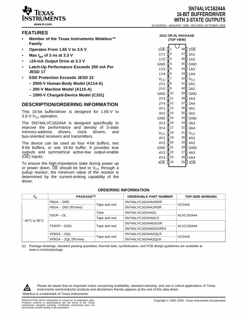
GQL OR ZQL PACKAGE(TOP VIEW)
JHGFEDCBA
21 3 4 65
K
ABC
GRD OR ZRD PACKAGE(TOP VIEW)
J
H
G
F
E
D
C
B
A
21 3 4 65
SN74ALVC16244A16-BIT BUFFER/DRIVERWITH 3-STATE OUTPUTSSCAS250O–JANUARY 1993–REVISED OCTOBER 2005
TERMINAL ASSIGNMENTS (1)
(56-Ball GQL/ZQL Package)
1 2 3 4 5 6
A 1OE NC NC NC NC 2OE
B 1Y2 1Y1 GND GND 1A1 1A2
C 1Y4 1Y3 VCC VCC 1A3 1A4
D 2Y2 2Y1 GND GND 2A1 2A2
E 2Y4 2Y3 2A3 2A4
F 3Y1 3Y2 3A2 3A1
G 3Y3 3Y4 GND GND 3A4 3A3
H 4Y1 4Y2 VCC VCC 4A2 4A1
J 4Y3 4Y4 GND GND 4A4 4A3
K 4OE NC NC NC NC 3OE
ABC (1) NC – No internal connection
TERMINAL ASSIGNMENTS (1)
(54-Ball GRD/ZRD Package)
1 2 3 4 5 6
A 1Y1 NC 1OE 2OE NC 1A1
B 1Y3 1Y2 NC NC 1A2 1A3
C 2Y1 1Y4 VCC VCC 1A4 2A1
D 2Y3 2Y2 GND GND 2A2 2A3
E 3Y1 2Y4 GND GND 2A4 3A1
F 3Y3 3Y2 GND GND 3A2 3A3
G 4Y1 3Y4 VCC VCC 3A4 4A1
H 4Y3 4Y2 NC NC 4A2 4A3
J 4Y4 NC 4OE 3OE NC 4A4
(1) NC – No internal connectionxxxxx
FUNCTION TABLE(EACH 4-BIT BUFFER)
INPUTS OUTPUTYOE A
L H H
L L L
H X Z
2

www.ti.com
1OE
1A1
1A2
1A3
1A4
1Y1
1Y2
1Y3
1Y4
1
47
46
44
43
2
3
5
6
2OE
2A1
2A2
2A3
2A4
2Y1
2Y2
2Y3
2Y4
48
41
40
38
37
8
9
11
12
3OE
3A1
3A2
3A3
3A4
3Y1
3Y2
3Y3
3Y4
25
36
35
33
32
13
14
16
17
4OE
4A1
4A2
4A3
4A4
4Y1
4Y2
4Y3
4Y4
24
30
29
27
26
19
20
22
23
Pin numbers shown are for the DGG and DL packages.
Absolute Maximum Ratings (1)
SN74ALVC16244A16-BIT BUFFER/DRIVER
WITH 3-STATE OUTPUTSSCAS250O–JANUARY 1993–REVISED OCTOBER 2005
LOGIC DIAGRAM (POSITIVE LOGIC)
over operating free-air temperature range (unless otherwise noted)
MIN MAX UNIT
VCC Supply voltage range –0.5 4.6 V
VI Input voltage range (2) Control Inputs (3) –0.5 VCC + 0.5 V
Data Inputs -0.5 4.6
VO Output voltage range (2) (3) –0.5 VCC + 0.5 V
IIK Input clamp current VI < 0 –50 mA
IOK Output clamp current VO < 0 –50 mA
IO Continuous output current ±50 mA
Continuous current through each VCC or GND ±100 mA
DGG package 70
DL package 63θJA Package thermal impedance (4) °C/W
GQL/ZQL package 42
GRD/ZRD package 36
Tstg Storage temperature range –65 150 °C
(1) Stresses beyond those listed under "absolute maximum ratings" may cause permanent damage to the device. These are stress ratingsonly, and functional operation of the device at these or any other conditions beyond those indicated under "recommended operatingconditions" is not implied. Exposure to absolute-maximum-rated conditions for extended periods may affect device reliability.
(2) The input negative-voltage and output voltage ratings may be exceeded if the input and output current ratings are observed.(3) This value is limited to 4.6 V maximum.(4) The package thermal impedance is calculated in accordance with JESD 51-7.
3

www.ti.com
Recommended Operating Conditions (1)
Electrical Characteristics
SN74ALVC16244A16-BIT BUFFER/DRIVERWITH 3-STATE OUTPUTSSCAS250O–JANUARY 1993–REVISED OCTOBER 2005
MIN MAX UNIT
VCC Supply voltage 1.65 3.6 V
VCC = 1.65 V to 1.95 V 0.65 × VCC
VIH High-level input voltage VCC = 2.3 V to 2.7 V 1.7 V
VCC = 2.7 V to 3.6 V 2
VCC = 1.65 V to 1.95 V 0.35 × VCC
VIL Low-level input voltage VCC = 2.3 V to 2.7 V 0.7 V
VCC = 2.7 V to 3.6 V 0.8
Control Inputs 0 VCCVI Input voltage V
Data Inputs 0 3.6
VO Output voltage 0 VCC V
VCC = 1.65 V –4
VCC = 2.3 V –12IOH High-level output current mA
VCC = 2.7 V –12
VCC = 3 V –24
VCC = 1.65 V 4
VCC = 2.3 V 12IOL Low-level output current mA
VCC = 2.7 V 12
VCC = 3 V 24
∆t/∆v Input transition rise or fall rate 10 ns/V
TA Operating free-air temperature –40 85 °C
(1) All unused inputs of the device must be held at VCC or GND to ensure proper device operation. Refer to the TI application report,Implications of Slow or Floating CMOS Inputs, literature number SCBA004.
over recommended operating free-air temperature range (unless otherwise noted)
PARAMETER TEST CONDITIONS VCC MIN TYP (1) MAX UNIT
IOH = –100 µA 1.65 V to 3.6 V VCC – 0.2
IOH = –4 mA 1.65 V 1.2
IOH = –6 mA 2.3 V 2
VOH 2.3 V 1.7 V
IOH = –12 mA 2.7 V 2.2
3 V 2.4
IOH = –24 mA 3 V 2
IOL = 100 µA 1.65 V to 3.6 V 0.2
IOL = 4 mA 1.65 V 0.45
IOL = 6 mA 2.3 V 0.4VOL V
2.3 V 0.7IOL = 12 mA
2.7 V 0.4
IOL = 24 mA 3 V 0.55
II VI = VCC or GND 3.6 V ±5 µA
IOZ VO = VCC or GND 3.6 V ±10 µA
ICC VI = VCC or GND, IO = 0 3.6 V 40 µA
Other inputs at VCC or∆ICC One input at VCC – 0.6 V, 3 V to 3.6 V 750 µAGND
Control inputs 3Ci VI = VCC or GND 3.3 V pF
Data inputs 6
(1) All typical values are at VCC = 3.3 V, TA = 25°C.
4

www.ti.com
Switching Characteristics
Operating Characteristics
SN74ALVC16244A16-BIT BUFFER/DRIVER
WITH 3-STATE OUTPUTSSCAS250O–JANUARY 1993–REVISED OCTOBER 2005
Electrical Characteristics (continued)
over recommended operating free-air temperature range (unless otherwise noted)
PARAMETER TEST CONDITIONS VCC MIN TYP (1) MAX UNIT
Co Outputs VO = VCC or GND 3.3 V 7 pF
over recommended operating free-air temperature range (unless otherwise noted) (see Figure 1)
VCC = 2.5 V VCC = 3.3 VVCC = 1.8 V VCC = 2.7 VFROM TO ± 0.2 V ± 0.3 VPARAMETER UNIT(INPUT) (OUTPUT)TYP MIN MAX MIN MAX MIN MAX
tpd A Y (1) 1 3.7 3.6 1 3 ns
ten OE Y (1) 1 5.7 5.4 1 4.4 ns
tdis OE Y (1) 1 5.2 4.6 1 4.1 ns
(1) This information was not available at the time of publication.
TA = 25°C
VCC = 1.8 V VCC = 2.5 V VCC = 3.3 VTESTPARAMETER UNITCONDITIONS TYP TYP TYP
Outputs enabled (1) 16 19Power dissipationCpd CL = 50 pF, f = 10 MHz pFcapacitance Outputs disabled (1) 4 5
(1) This information was not available at the time of publication.
5

www.ti.com
PARAMETER MEASUREMENT INFORMATION
VM
VM
VMVM
VMVM
VMVM
VOH
VOL
thtsu
From OutputUnder Test
CL(see Note A)
LOAD CIRCUIT
S1 Open
GND
RL
RL
OutputControl
(low-levelenabling)
OutputWaveform 1S1 at VLOAD(see Note B)
OutputWaveform 2
S1 at GND(see Note B)
tPZL
tPZH
tPLZ
tPHZ
0 V
VOL + V∆
VOH − V∆
0 V
VI
0 V
0 V
tw
VIVI
VOLTAGE WAVEFORMSSETUP AND HOLD TIMES
VOLTAGE WAVEFORMSPULSE DURATION
VOLTAGE WAVEFORMSENABLE AND DISABLE TIMES
TimingInput
DataInput
Input
tpdtPLZ/tPZLtPHZ/tPZH
OpenVLOADGND
TEST S1
NOTES: A. CL includes probe and jig capacitance.B. Waveform 1 is for an output with internal conditions such that the output is low, except when disabled by the output control.
Waveform 2 is for an output with internal conditions such that the output is high, except when disabled by the output control.C. All input pulses are supplied by generators having the following characteristics: PRR ≤ 10 MHz, ZO = 50 Ω.D. The outputs are measured one at a time, with one transition per measurement.E. tPLZ and tPHZ are the same as tdis.F. tPZL and tPZH are the same as ten.G. tPLH and tPHL are the same as tpd.H. All parameters and waveforms are not applicable to all devices.
0 V
VI
VM
tPHL
VM VM
VI
0 V
VOH
VOL
Input
Output
VOLTAGE WAVEFORMSPROPAGATION DELAY TIMES
VM VM
tPLH
VLOAD
VLOAD/2
1.8 V2.5 V ± 0.2 V
2.7 V3.3 V ± 0.3 V
1 kΩ500 Ω500 Ω500 Ω
VCC RL
2 × VCC2 × VCC
6 V6 V
VLOAD CL
30 pF30 pF50 pF50 pF
0.15 V0.15 V0.3 V0.3 V
V∆
VCCVCC2.7 V2.7 V
VI
VCC/2VCC/21.5 V1.5 V
VMtr/tf
≤2 ns≤2 ns
≤2.5 ns≤2.5 ns
INPUT
SN74ALVC16244A16-BIT BUFFER/DRIVERWITH 3-STATE OUTPUTSSCAS250O–JANUARY 1993–REVISED OCTOBER 2005
Figure 1. Load Circuit and Voltage Waveforms
6
PACKAGE OPTION ADDENDUM
www.ti.com 24-Aug-2018
Addendum-Page 1
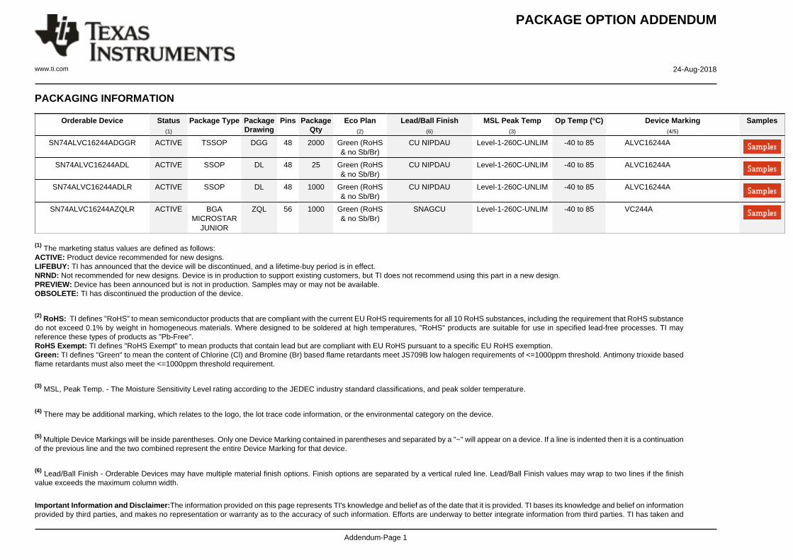
PACKAGING INFORMATION
Orderable Device Status(1)
Package Type PackageDrawing
Pins PackageQty
Eco Plan(2)
Lead/Ball Finish(6)
MSL Peak Temp(3)
Op Temp (°C) Device Marking(4/5)
Samples
SN74ALVC16244ADGGR ACTIVE TSSOP DGG 48 2000 Green (RoHS& no Sb/Br)
CU NIPDAU Level-1-260C-UNLIM -40 to 85 ALVC16244A
SN74ALVC16244ADL ACTIVE SSOP DL 48 25 Green (RoHS& no Sb/Br)
CU NIPDAU Level-1-260C-UNLIM -40 to 85 ALVC16244A
SN74ALVC16244ADLR ACTIVE SSOP DL 48 1000 Green (RoHS& no Sb/Br)
CU NIPDAU Level-1-260C-UNLIM -40 to 85 ALVC16244A
SN74ALVC16244AZQLR ACTIVE BGAMICROSTAR
JUNIOR
ZQL 56 1000 Green (RoHS& no Sb/Br)
SNAGCU Level-1-260C-UNLIM -40 to 85 VC244A
(1) The marketing status values are defined as follows:ACTIVE: Product device recommended for new designs.LIFEBUY: TI has announced that the device will be discontinued, and a lifetime-buy period is in effect.NRND: Not recommended for new designs. Device is in production to support existing customers, but TI does not recommend using this part in a new design.PREVIEW: Device has been announced but is not in production. Samples may or may not be available.OBSOLETE: TI has discontinued the production of the device.
(2) RoHS: TI defines "RoHS" to mean semiconductor products that are compliant with the current EU RoHS requirements for all 10 RoHS substances, including the requirement that RoHS substancedo not exceed 0.1% by weight in homogeneous materials. Where designed to be soldered at high temperatures, "RoHS" products are suitable for use in specified lead-free processes. TI mayreference these types of products as "Pb-Free".RoHS Exempt: TI defines "RoHS Exempt" to mean products that contain lead but are compliant with EU RoHS pursuant to a specific EU RoHS exemption.Green: TI defines "Green" to mean the content of Chlorine (Cl) and Bromine (Br) based flame retardants meet JS709B low halogen requirements of <=1000ppm threshold. Antimony trioxide basedflame retardants must also meet the <=1000ppm threshold requirement.
(3) MSL, Peak Temp. - The Moisture Sensitivity Level rating according to the JEDEC industry standard classifications, and peak solder temperature.
(4) There may be additional marking, which relates to the logo, the lot trace code information, or the environmental category on the device.
(5) Multiple Device Markings will be inside parentheses. Only one Device Marking contained in parentheses and separated by a "~" will appear on a device. If a line is indented then it is a continuationof the previous line and the two combined represent the entire Device Marking for that device.
(6) Lead/Ball Finish - Orderable Devices may have multiple material finish options. Finish options are separated by a vertical ruled line. Lead/Ball Finish values may wrap to two lines if the finishvalue exceeds the maximum column width.
Important Information and Disclaimer:The information provided on this page represents TI's knowledge and belief as of the date that it is provided. TI bases its knowledge and belief on informationprovided by third parties, and makes no representation or warranty as to the accuracy of such information. Efforts are underway to better integrate information from third parties. TI has taken and

PACKAGE OPTION ADDENDUM
www.ti.com 24-Aug-2018
Addendum-Page 2
continues to take reasonable steps to provide representative and accurate information but may not have conducted destructive testing or chemical analysis on incoming materials and chemicals.TI and TI suppliers consider certain information to be proprietary, and thus CAS numbers and other limited information may not be available for release.
In no event shall TI's liability arising out of such information exceed the total purchase price of the TI part(s) at issue in this document sold by TI to Customer on an annual basis.

TAPE AND REEL INFORMATION
*All dimensions are nominal
Device PackageType
PackageDrawing
Pins SPQ ReelDiameter
(mm)
ReelWidth
W1 (mm)
A0(mm)
B0(mm)
K0(mm)
P1(mm)
W(mm)
Pin1Quadrant
SN74ALVC16244ADGGR TSSOP DGG 48 2000 330.0 24.4 8.6 13.0 1.8 12.0 24.0 Q1
SN74ALVC16244ADLR SSOP DL 48 1000 330.0 32.4 11.35 16.2 3.1 16.0 32.0 Q1
SN74ALVC16244AZQLR BGA MI CROSTA
R JUNI OR
ZQL 56 1000 330.0 16.4 4.8 7.3 1.5 8.0 16.0 Q1
PACKAGE MATERIALS INFORMATION
www.ti.com 11-Mar-2017
Pack Materials-Page 1

*All dimensions are nominal
Device Package Type Package Drawing Pins SPQ Length (mm) Width (mm) Height (mm)
SN74ALVC16244ADGGR TSSOP DGG 48 2000 367.0 367.0 45.0
SN74ALVC16244ADLR SSOP DL 48 1000 367.0 367.0 55.0
SN74ALVC16244AZQLR BGA MICROSTARJUNIOR
ZQL 56 1000 336.6 336.6 28.6
PACKAGE MATERIALS INFORMATION
www.ti.com 11-Mar-2017
Pack Materials-Page 2

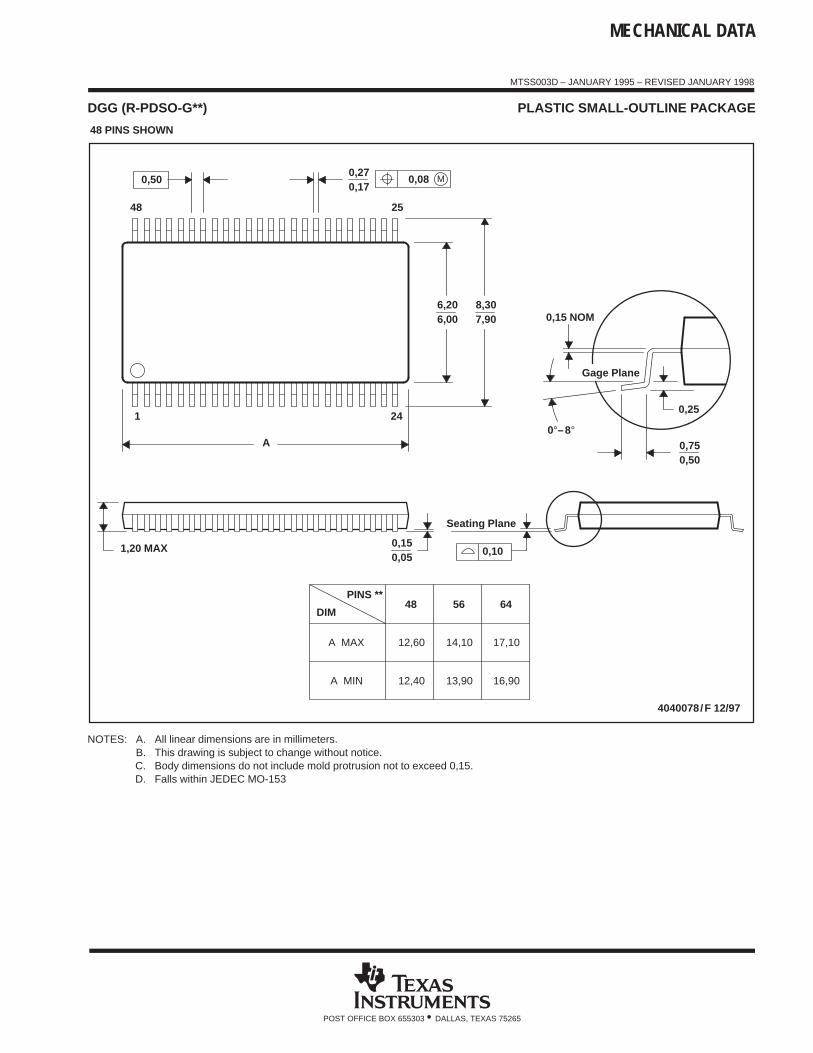
MECHANICAL DATA
MTSS003D – JANUARY 1995 – REVISED JANUARY 1998
POST OFFICE BOX 655303 • DALLAS, TEXAS 75265
DGG (R-PDSO-G**) PLASTIC SMALL-OUTLINE PACKAGE
4040078/F 12/97
48 PINS SHOWN
0,25
0,15 NOM
Gage Plane
6,006,20 8,30
7,90
0,750,50
Seating Plane
25
0,270,17
24
A
48
1
1,20 MAX
M0,08
0,10
0,50
0°–8°
56
14,10
13,90
48DIM
A MAX
A MIN
PINS **
12,40
12,60
64
17,10
16,90
0,150,05
NOTES: A. All linear dimensions are in millimeters.B. This drawing is subject to change without notice.C. Body dimensions do not include mold protrusion not to exceed 0,15.D. Falls within JEDEC MO-153
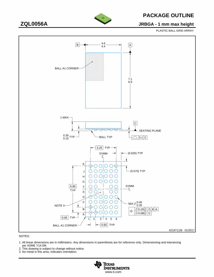
www.ti.com
PACKAGE OUTLINE
C
1 MAX
TYP0.350.15
5.85TYP
3.25 TYP
0.65 TYP
0.65 TYP
56X 0.450.35
B 4.64.4 A
7.16.9
(0.625) TYP
(0.575) TYP
JRBGA - 1 mm max heightZQL0056APLASTIC BALL GRID ARRAY
4219711/B 01/2017
NOTES: 1. All linear dimensions are in millimeters. Any dimensions in parenthesis are for reference only. Dimensioning and tolerancing per ASME Y14.5M. 2. This drawing is subject to change without notice. 3. No metal in this area, indicates orientation.
BALL A1 CORNER
SEATING PLANE
BALL TYP 0.1 C
0.15 C B A0.08 C
SYMM
SYMM
BALL A1 CORNER
K
C
D
E
F
G
H
J
1 2 3 4 5 6
A
BNOTE 3
SCALE 2.100

www.ti.com
EXAMPLE BOARD LAYOUT
56X ( 0.33)(0.65) TYP
(0.65) TYP
( 0.33)METAL
0.05 MAXSOLDER MASKOPENING
METAL UNDERSOLDER MASK
( 0.33)SOLDER MASKOPENING
0.05 MIN
JRBGA - 1 mm max heightZQL0056APLASTIC BALL GRID ARRAY
4219711/B 01/2017
NOTES: (continued) 4. Final dimensions may vary due to manufacturing tolerance considerations and also routing constraints. For information, see Texas Instruments literature number SPRAA99 (www.ti.com/lit/spraa99).
SYMM
SYMM
LAND PATTERN EXAMPLEEXPOSED METAL SHOWN
SCALE:15X
1 2 3 4 5 6
A
C
D
E
F
G
H
J
K
B
NON-SOLDER MASKDEFINED
(PREFERRED)
SOLDER MASK DETAILSNOT TO SCALE
EXPOSED METAL
SOLDER MASKDEFINED
EXPOSED METAL

www.ti.com
EXAMPLE STENCIL DESIGN
(0.65) TYP
(0.65) TYP56X ( 0.33)
JRBGA - 1 mm max heightZQL0056APLASTIC BALL GRID ARRAY
4219711/B 01/2017
NOTES: (continued) 5. Laser cutting apertures with trapezoidal walls and rounded corners may offer better paste release.
SOLDER PASTE EXAMPLEBASED ON 0.125 mm THICK STENCIL
SCALE:15X
SYMM
SYMM
1 2 3 4 5 6
A
C
D
E
F
G
H
J
K
B
IMPORTANT NOTICE
Texas Instruments Incorporated (TI) reserves the right to make corrections, enhancements, improvements and other changes to itssemiconductor products and services per JESD46, latest issue, and to discontinue any product or service per JESD48, latest issue. Buyersshould obtain the latest relevant information before placing orders and should verify that such information is current and complete.TI’s published terms of sale for semiconductor products (http://www.ti.com/sc/docs/stdterms.htm) apply to the sale of packaged integratedcircuit products that TI has qualified and released to market. Additional terms may apply to the use or sale of other types of TI products andservices.Reproduction of significant portions of TI information in TI data sheets is permissible only if reproduction is without alteration and isaccompanied by all associated warranties, conditions, limitations, and notices. TI is not responsible or liable for such reproduceddocumentation. Information of third parties may be subject to additional restrictions. Resale of TI products or services with statementsdifferent from or beyond the parameters stated by TI for that product or service voids all express and any implied warranties for theassociated TI product or service and is an unfair and deceptive business practice. TI is not responsible or liable for any such statements.Buyers and others who are developing systems that incorporate TI products (collectively, “Designers”) understand and agree that Designersremain responsible for using their independent analysis, evaluation and judgment in designing their applications and that Designers havefull and exclusive responsibility to assure the safety of Designers' applications and compliance of their applications (and of all TI productsused in or for Designers’ applications) with all applicable regulations, laws and other applicable requirements. Designer represents that, withrespect to their applications, Designer has all the necessary expertise to create and implement safeguards that (1) anticipate dangerousconsequences of failures, (2) monitor failures and their consequences, and (3) lessen the likelihood of failures that might cause harm andtake appropriate actions. Designer agrees that prior to using or distributing any applications that include TI products, Designer willthoroughly test such applications and the functionality of such TI products as used in such applications.TI’s provision of technical, application or other design advice, quality characterization, reliability data or other services or information,including, but not limited to, reference designs and materials relating to evaluation modules, (collectively, “TI Resources”) are intended toassist designers who are developing applications that incorporate TI products; by downloading, accessing or using TI Resources in anyway, Designer (individually or, if Designer is acting on behalf of a company, Designer’s company) agrees to use any particular TI Resourcesolely for this purpose and subject to the terms of this Notice.TI’s provision of TI Resources does not expand or otherwise alter TI’s applicable published warranties or warranty disclaimers for TIproducts, and no additional obligations or liabilities arise from TI providing such TI Resources. TI reserves the right to make corrections,enhancements, improvements and other changes to its TI Resources. TI has not conducted any testing other than that specificallydescribed in the published documentation for a particular TI Resource.Designer is authorized to use, copy and modify any individual TI Resource only in connection with the development of applications thatinclude the TI product(s) identified in such TI Resource. NO OTHER LICENSE, EXPRESS OR IMPLIED, BY ESTOPPEL OR OTHERWISETO ANY OTHER TI INTELLECTUAL PROPERTY RIGHT, AND NO LICENSE TO ANY TECHNOLOGY OR INTELLECTUAL PROPERTYRIGHT OF TI OR ANY THIRD PARTY IS GRANTED HEREIN, including but not limited to any patent right, copyright, mask work right, orother intellectual property right relating to any combination, machine, or process in which TI products or services are used. Informationregarding or referencing third-party products or services does not constitute a license to use such products or services, or a warranty orendorsement thereof. Use of TI Resources may require a license from a third party under the patents or other intellectual property of thethird party, or a license from TI under the patents or other intellectual property of TI.TI RESOURCES ARE PROVIDED “AS IS” AND WITH ALL FAULTS. TI DISCLAIMS ALL OTHER WARRANTIES ORREPRESENTATIONS, EXPRESS OR IMPLIED, REGARDING RESOURCES OR USE THEREOF, INCLUDING BUT NOT LIMITED TOACCURACY OR COMPLETENESS, TITLE, ANY EPIDEMIC FAILURE WARRANTY AND ANY IMPLIED WARRANTIES OFMERCHANTABILITY, FITNESS FOR A PARTICULAR PURPOSE, AND NON-INFRINGEMENT OF ANY THIRD PARTY INTELLECTUALPROPERTY RIGHTS. TI SHALL NOT BE LIABLE FOR AND SHALL NOT DEFEND OR INDEMNIFY DESIGNER AGAINST ANY CLAIM,INCLUDING BUT NOT LIMITED TO ANY INFRINGEMENT CLAIM THAT RELATES TO OR IS BASED ON ANY COMBINATION OFPRODUCTS EVEN IF DESCRIBED IN TI RESOURCES OR OTHERWISE. IN NO EVENT SHALL TI BE LIABLE FOR ANY ACTUAL,DIRECT, SPECIAL, COLLATERAL, INDIRECT, PUNITIVE, INCIDENTAL, CONSEQUENTIAL OR EXEMPLARY DAMAGES INCONNECTION WITH OR ARISING OUT OF TI RESOURCES OR USE THEREOF, AND REGARDLESS OF WHETHER TI HAS BEENADVISED OF THE POSSIBILITY OF SUCH DAMAGES.Unless TI has explicitly designated an individual product as meeting the requirements of a particular industry standard (e.g., ISO/TS 16949and ISO 26262), TI is not responsible for any failure to meet such industry standard requirements.Where TI specifically promotes products as facilitating functional safety or as compliant with industry functional safety standards, suchproducts are intended to help enable customers to design and create their own applications that meet applicable functional safety standardsand requirements. Using products in an application does not by itself establish any safety features in the application. Designers mustensure compliance with safety-related requirements and standards applicable to their applications. Designer may not use any TI products inlife-critical medical equipment unless authorized officers of the parties have executed a special contract specifically governing such use.Life-critical medical equipment is medical equipment where failure of such equipment would cause serious bodily injury or death (e.g., lifesupport, pacemakers, defibrillators, heart pumps, neurostimulators, and implantables). Such equipment includes, without limitation, allmedical devices identified by the U.S. Food and Drug Administration as Class III devices and equivalent classifications outside the U.S.TI may expressly designate certain products as completing a particular qualification (e.g., Q100, Military Grade, or Enhanced Product).Designers agree that it has the necessary expertise to select the product with the appropriate qualification designation for their applicationsand that proper product selection is at Designers’ own risk. Designers are solely responsible for compliance with all legal and regulatoryrequirements in connection with such selection.Designer will fully indemnify TI and its representatives against any damages, costs, losses, and/or liabilities arising out of Designer’s non-compliance with the terms and provisions of this Notice.
Mailing Address: Texas Instruments, Post Office Box 655303, Dallas, Texas 75265Copyright © 2018, Texas Instruments Incorporated