
SMTA 2013 0.3 mm pitch kochanowski rev 6 published
11
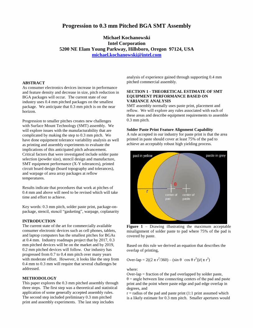
Progression to 0.3 mm Pitched BGA SMT Assembly Michael Kochanowski Intel Corporation 5200 NE Elam Young Parkway, Hillsboro, Oregon 97124, USA [email protected] ABSTRACT As consumer electronics devices increase in performance and feature density and decrease in size, pitch reduction in BGA packages will occur. The current state of our industry uses 0.4 mm pitched packages on the smallest package. We anticipate that 0.3 mm pitch is on the near horizon. Progression to smaller pitches creates new challenges with Surface Mount Technology (SMT) assembly. We will explore issues with the manufacturability that are complicated by making the step to 0.3 mm pitch. We have done equipment tolerance variability analysis as well as printing and assembly experiments to evaluate the implications of this anticipated pitch advancement. Critical factors that were investigated include solder paste selection (powder size), stencil design and manufacture, SMT equipment performance (X-Y tolerances), printed circuit board design (board topography and tolerances), and warpage of area array packages at reflow temperatures. Results indicate that procedures that work at pitches of 0.4 mm and above will need to be revised which will take time and effort to achieve. Key words: 0.3 mm pitch, solder paste print, package-on- package, stencil, stencil “gasketing”, warpage, coplanarity INTRODUCTION The current state of the art for commercially available consumer electronic devices such as cell phones, tablets, and laptop computers has the smallest pitches for BGAs at 0.4 mm. Industry roadmaps project that by 2017, 0.3 mm pitched devices will be on the market and by 2019, 0.2 mm pitched devices will follow. Our industry has progressed from 0.7 to 0.4 mm pitch over many years with moderate effort. However, it looks like the step from 0.4 mm to 0.3 mm will require that several challenges be addressed. METHODOLOGY This paper explores the 0.3 mm pitched assembly through three steps. The first step was a theoretical and statistical application of some generally accepted assembly rules. The second step included preliminary 0.3 mm pitched print and assembly experiments. The last step includes analysis of experience gained through supporting 0.4 mm pitched commercial assembly. SECTION 1 - THEORETICAL ESTIMATE OF SMT EQUIPMENT PERFORMANCE BASED ON VARIANCE ANALYSIS SMT assembly normally uses paste print, placement and reflow. We will explore any rules associated with each of these areas and describe equipment requirements to assemble 0.3 mm pitch. Solder Paste Print Feature Alignment Capability A rule accepted in our industry for paste print is that the area printed in paste should cover at least 75% of the pad to achieve an acceptably robust high yielding process. Figure 1 – Drawing illustrating the maximum acceptable misalignment of solder paste to pad where 75% of the pad is covered by paste. Based on this rule we derived an equation that describes the overlap of printing, Over-lap = 2((2 π r 2 /360) – (sin θ . cos θ r 2 ))/( π r 2 ) where: Over-lap = fraction of the pad overlapped by solder paste, θ = angle between line connecting centers of the pad and paste print and the point where paste edge and pad edge overlap in degrees, and r = radius of the pad and paste print (1:1 print assumed which is a likely estimate for 0.3 mm pitch. Smaller apertures would
-
Upload
michael-kochanowski -
Category
Documents
-
view
89 -
download
0
Transcript of SMTA 2013 0.3 mm pitch kochanowski rev 6 published
Progression to 0.3 mm Pitched BGA SMT Assembly
Michael Kochanowski
Intel Corporation
5200 NE Elam Young Parkway, Hillsboro, Oregon 97124, USA
ABSTRACT
As consumer electronics devices increase in performance
and feature density and decrease in size, pitch reduction in
BGA packages will occur. The current state of our
industry uses 0.4 mm pitched packages on the smallest
package. We anticipate that 0.3 mm pitch is on the near
horizon.
Progression to smaller pitches creates new challenges
with Surface Mount Technology (SMT) assembly. We
will explore issues with the manufacturability that are
complicated by making the step to 0.3 mm pitch. We
have done equipment tolerance variability analysis as well
as printing and assembly experiments to evaluate the
implications of this anticipated pitch advancement.
Critical factors that were investigated include solder paste
selection (powder size), stencil design and manufacture,
SMT equipment performance (X-Y tolerances), printed
circuit board design (board topography and tolerances),
and warpage of area array packages at reflow
temperatures.
Results indicate that procedures that work at pitches of
0.4 mm and above will need to be revised which will take
time and effort to achieve.
Key words: 0.3 mm pitch, solder paste print, package-on-
package, stencil, stencil “gasketing”, warpage, coplanarity
INTRODUCTION
The current state of the art for commercially available
consumer electronic devices such as cell phones, tablets,
and laptop computers has the smallest pitches for BGAs
at 0.4 mm. Industry roadmaps project that by 2017, 0.3
mm pitched devices will be on the market and by 2019,
0.2 mm pitched devices will follow. Our industry has
progressed from 0.7 to 0.4 mm pitch over many years
with moderate effort. However, it looks like the step from
0.4 mm to 0.3 mm will require that several challenges be
addressed.
METHODOLOGY
This paper explores the 0.3 mm pitched assembly through
three steps. The first step was a theoretical and statistical
application of some generally accepted assembly rules.
The second step included preliminary 0.3 mm pitched
print and assembly experiments. The last step includes
analysis of experience gained through supporting 0.4 mm
pitched commercial assembly.
SECTION 1 - THEORETICAL ESTIMATE OF SMT
EQUIPMENT PERFORMANCE BASED ON
VARIANCE ANALYSIS
SMT assembly normally uses paste print, placement and
reflow. We will explore any rules associated with each of
these areas and describe equipment requirements to assemble
0.3 mm pitch.
Solder Paste Print Feature Alignment Capability
A rule accepted in our industry for paste print is that the area
printed in paste should cover at least 75% of the pad to
achieve an acceptably robust high yielding process.
Figure 1 – Drawing illustrating the maximum acceptable
misalignment of solder paste to pad where 75% of the pad is
covered by paste.
Based on this rule we derived an equation that describes the
overlap of printing,
Over-lap = 2((2 π r2/360) – (sin θ
. cos θ r
2))/(
π r
2)
where:
Over-lap = fraction of the pad overlapped by solder paste,
θ = angle between line connecting centers of the pad and paste
print and the point where paste edge and pad edge overlap in
degrees, and
r = radius of the pad and paste print (1:1 print assumed which
is a likely estimate for 0.3 mm pitch. Smaller apertures would

create less than optimal print volume and larger apertures
risk bridging defects.).
To meet the 75% coverage rule we solve and get an angle,
θ, of 78.6º. Our estimates are that for 0.3 mm pitch that 7
mil pads on a board with a 7 mil stencil aperture would be
a likely geometry. To achieve this overlap the maximum
allowable offset between center of the pad and the center
of the print is 2 . cos θ
. r (derived from geometry) which
equals 1.38 mil. Therefore, ± 1.38 mils is the maximum
offset in print alignment that we can tolerate and still have
an SMT process where we would expect to have good
yield. We will use this result later in our analysis.
The relationship that describes the location of print on the
board is a sum of the alignment of the printer to the board,
the alignment of the board features across the board, the
alignment of the stencil features on the stencil and
alignment due to stencil flex during printing.
First, we calculate the variation in the printing process.
To calculate the total variance of the printing process we
just add the variance of the individual components as
follows:
σ2
total printing = σ2
printer alignment + σ2
PCB features +
σ2
stencil features + σ2
stencil flex/movement during print
Note: For simplicity our analysis is done in only one
dimension. (Our analysis was done in X only versus X
and Y combined.) To be exact we would look at the
performance in two dimensions (Z = (X2 + Y
2)
½) but the
math gets very complicated. In another case, we did this
analysis in the combined X and Y dimensions but we
found that the conclusion with a one dimensional
approach is effectively the same.
Next, we will apply this tolerance to the variation in print
conditions that we would expect to find in normal good
equipment used in the assembly of smart phones, tablets
computers.
We used the expertise from various board, machine and
stencil experts to estimate the variance of the components
as follows:
1. σ2
printer alignment = (0.492 mil /6)2 = 0.006727
mil2 (based on the specs of a DEK Galaxy
machine)
2. σ2
PCB features = (0.430 mil /4)2 = 0.01156 mil
2
(based on board class 2 feature tolerances scaled
to a 5”x5” board size)
3. σ2
stencil features = (0.3 mil /4)2 = 0.005625 mil
2
(based on conversations with various stencil
manufacturers)
4. σ2
stencil flex/movement during print = (1.0 mil /4)2 =
0.0625 mil2 (based on conversations with a
printing machine manufacturer).
Adding all of the variances, we get a total variance of the
printing process as σ2
total printing = 0.0864 mil2 and σtotal
printing = 0.294 mil. When we apply a Cpk rule of 1.33, the
variability in the alignment of the printing process would be ±
4. σ total printing = ± 1.176 mils. This analysis confirms that the
cumulative variability of the solder paste printer, the printed
circuit board, the stencil features and the stencil movement
during printing is within the allowed calculated tolerance of ±
1.38 mil. However, we are right at the margin of being
acceptable.
Our conclusion is that we expect that the printing step with the
quality of assembly equipment generally used by reputable
ODMs, with normal class 2 board quality and with normal
stencil tolerances to be just sufficient for 0.3 mm pitch
assembly in X-Y alignment.
It should also be noted that of the total variance in the printing
process, about 72% of the variance comes from stencil
flex/movement. Printer alignment, PCB features, and stencil
features account for only 8, 13 and 7% of the variance,
respectively. Although these numbers come from estimates,
we believe that the order of magnitude their impact is realistic.
What this means is that the flex and movement of the stencil
in the printing machine is by far the largest component of
variation in this system. The dynamic movement of the stencil
in the printer during its operation is becoming more relevant at
this low pitch and is the limiter to the progression toward finer
pitches.
At 0.3 mm pitch, the X-Y location of the print location is
expected to move from board to board (with commonly
available equipment). An example of this variation is shown
in Figure 2. Notice that the first print completely covers the
pad and another print with the same printer set up but a few
prints later the print has shifted to the right so that the edges of
the copper pads are exposed. We found that this kind of drift
is routinely when working with some boards at this pitch.
Figure 2 – Example of Print Position Variation on 0.3 mm
Pitch BGA Site.
BGA Part Placement Alignment Capability
Similar to print, a rule in SMT is that when a BGA is placed,
the solder ball should cover at least 50% of the pad. (see
Figure 3)

Figure 3 – Drawing illustrating the maximum acceptable
misalignment of BGA solder ball to pad where 50% of the
pad is covered by the area projection of the solder ball.
We apply the same mathematical analysis to this system
as we did in the prior solder paste print situation. (A good
estimate for 0.3 mm pitched geometries is a 7 mil pad
diameter and a 7 mil solder ball diameter.) In this case
we find that ± 2.83 mil is the maximum placement offset
that we can tolerate and still have an SMT process where
we would expect to have good yield.
Similar to before, we apply this tolerance to the variation
in placement conditions that we would expect to find in
state of the art equipment in the assembly of smart
phones, tablets and laptop computers.
To calculate the total variance of the placement process
we just add the variance of the individual components as
follows:
σ2
total placement = σ2
placement positioning alignment +
σ2
PCB features + σ2
ball-to-ball
Again, using the expertise from various board and
machine vendors to estimate the variance of the
components as follows:
1. σ2
placement machine position alignment = (2.0 mil /4)2
= 0.25 mil2
(Universal GSM machine)
2. σ2
PCB features = (0.430 mil /4)2 = 0.01156 mil
2
(Based on board class 2 feature tolerances scaled
to a 5”x5” board size)
3. σ2
ball-to-ball ≈ 0 ≈ 0 mil2 (variation of balls
within the array respect to each other are
assumed to be negligible)
Adding all of the variances, we get a total variance of the
placement process as σ2
total placement = 0.26256 mil2 and
σtotal placement = 0.511 mil. When we apply a Cpk rule of
1.33, the variability in the alignment of the placement
process would be ± 4. σ total placement = ± 2.05 mils. Again, the
calculated accumulative variation of ± 2.05 mils is less than
the ± 2.83 mil allowable variation. The placement systems in
place at reputable quality ODMs are capable to assemble at
0.3 mm pitch.
It should also be noted that the placement step is more capable
statistically at 0.3 mm pitch than paste printing.
Ideal Paste Printing Mechanism
Before we continue we should discuss a mechanism for an
ideal solder paste print. Figure 4 animates this print event.
Figure 4 – Ideal Solder Paste Print Animation – View with
Stencil Engaged (above) followed by View with Stencil Lifted
(below)
In an ideal case, the stencil sits perfectly flat against the board
surface. After a pass of the squeegee, solder paste fills the
aperture and makes complete contact with the pad below.
Next, the printing machine lifts the stencil off of the board.
The adhesion force of the solder paste on the pad (represented
by the green line) is greater than the adhesion force of the
solder paste against the stencil wall (represented by the red
line) and the solder paste releases from the aperture.
“Gasketing” is defined as the ability of the stencil to form a
temporary seal with the board surface such that printed solder
paste has nowhere to flow other than on the intended pad
surface. Gasketing is key to proper print performance. So far
there is no way to quantify or measure the quality of gasketing
of a stencil/board/printer system.
All of the release-ratio rules around solder paste print are
predicated in a system that is dominated by these dynamics.

Unfortunately, as pitches get smaller, the scale of board
topography irregularities, board support and stencil flex
issues combine and challenge the ability to get proper
gasketing.
SECTION 2 - PRINTING EXPERIMENTS
TARGETING 0.30 MM PITCHED ARRAYS
We conducted several print screening studies to determine
what conditions may be more conducive to assembling
packages near 0.3mm pitch. A discussion of some of our
observation follows.
Stencil Design Screening Study
A screening study was done to see the repeatability of
solder prints with a variety of round aperture stencil
constructions targeted toward 0.30, 0.35 and 0.4 mm
pitched devices with some commonly use type 4 solder
pastes.(1)
A matrix of these stencils is shown in Table 1.
Table 1 – Stencil Construction for Screening Study
No Nomi
nal
Aperture
Diam
eter, mil
Mfg
Method
Thick,
mil
Treatments Area
Ratio
(from
measured
aperture
diameters)
1 10 laser 4 0.59
2 7 efab 3 0.58
3 7 efab 3 nano 0.55
4 7 laser 3 Ni plate,
nano 0.56
5 7 efab 4 nano 0.46
6 7 laser 4 Ni plate,
nano 0.39
7 8 efab 3 0.63
8 8 efab 3 nano 0.64
9 8 laser 3 Ni plate,
nano 0.65
10 8 efab 4 nano 0.53
11 8 laser 4 Ni plate,
nano 0.46
A summary of the volume of paste printed for multiple
prints with the fore stencils from Table 1 is shown in
Figure 5.
Figure 5 – Paste Volume Distribution for Various Stencil
Designs colored by Area Ratio (On the X-axis, print set up is
identified by stencil thickness in mils, stencil aperture
diameter in mils, and method of construction, respectively.)
We looked at the distributions of solder paste volume versus
the stencil types. Specifically we wanted stencils that both
delivered higher average solder paste volume and, more
importantly, minimal occurrences of prints below about 50
mil3. We know from prior work that with print volumes
below 50 mil3 we tend to get more small-solder-joint and open
defects as measured by a three dimensional X-ray and
electrically open joints. The stencil designs that most
consistently met this criterion were the 8 mil diameter
apertures with 3 mils of thickness. This was expected because
of the area ratio of these stencils compared to the others was
higher. (Colors closer to green have the most favorable area
ratios and those more white and red in the spectrum are less
desirable.)
It should be noted that the area ratio of these stencils (per
measurements) was 0.63 to 0.65. For stencil apertures, area
ratio is calculated as the area of the aperture opening divided
by area of the vertical aperture wall. More aperture opening
area helps promote adhesion of the solder slug to the board
and is helpful. More aperture wall area causes the slug of
paste to stick to the stencil and interferes with full release.
Higher the values of this ratio promote better paste release.
0.3 mm Pitch Specific Print Study
After the prior screening study, we conducted a second print
study with a 0.3 mm pitched land pattern. We chose to use a 3
mil thick, nominal 8 mil circular aperture electroformed
stencil and a same sized laser cut nickel plated, nano-coated
stencil based on the good results achieved in our first
screening study. The stencils that we acquired were as follows
in Table 2.
Table 2 – Stencil Construction for Comparison Study No Target
Aperture
Diameter
(mil)
Measured
Aperture
Diameter
(mils)
Manufacture
Method
Thickness
(mils)
1 8 8.38 laser, Ni 3

plated, nano-
coated
2 8 7.99 electroform 3
We used these stencils on a board with two 0.3 mm
pitched arrays with a 12x12 mm footprint and 1600 metal
defined OSP pads on a 4-layer, 40 mil thick board.
Figure 6 shows the footprint of one of the arrays.
Figure 6 – 0.3 mm Pitched Array Test Pattern – Metal
Defined Pads
In our experiment we printed with solder pastes with
powder of type 4, 4.5, 5 and 6, with identical flux
chemistry with each of the two stencils. We printed 15
times with each solder paste and stencil combination.
Prior to running our print study, we spent some time
optimizing the solder paste print for each stencil.
Unfortunately, we found that we could not get either of
these stencils to hold a consistent print without bridging
unless we cleaned the stencils frequently. We needed to
clean the laser cut, nickel plated, nano-coated stencil after
every second print to maintain a bridge free print. With
the electroformed stencil, we needed to clean the stencil
after every print to maintain a bridge free operation. This
cleaning frequency would not be acceptable for high
volume manufacturing.
In retrospect, this frequent need for stencil cleaning is
probably linked to less than optimal gasketing of the
stencil to the board surface. A test to validate the stencil
with good gasketing conditions will be discussed later in
this paper.
Bridging Caused By Stencil Cleaning Solvent
During these experiments, we noticed that we often got a
high incidence of bridging prints resulting immediately
after automated cleaning of our stencil unless we allowed
time for the stencil to dry. (see Figure 7)
Figure 7 – Typical Bridging Resulting in 0.3 mm Pitched
Printing Graphed by a Koh Young Solder Paste Inspection
Machine.
We observed that the cleaning solvent that we were using,
isopropyl alcohol, did not evaporate quickly from the stencil
aperture area. This small amount of remaining liquid seemed
to be enough to wet with the solder paste and cause a bridge.
We need to reevaluate our choice of stencil cleaning solvent
for a more volatile solvent that may evaporate quickly for high
speed assembly.
Print Performance versus Solder Paste Type
Most of the consumer electronics industry running 0.4, 0.5 and
0.6 mm pitched devices use type 4 solder paste. We anticipate
a need to migrate to finer particle size paste for pitches below
0.4 mm. Particle size versus type is listed in Table 3. (Particle
size ranges were obtained and from two different solder paste
suppliers and were the same. However, with paste types
beyond 4, particle size ranges may vary from supplier to
supplier, particularly for the half sized ranges.)
Table 3 – Solder Paste Particle Size versus Type
Paste Type Powder Particle Size
in microns
3 25-45
4 20-38
4.5 20-32
5 15-25
6 5-15
A graph showing the volume distribution of solder paste
volume as a function of the stencil construction and the solder
paste type is shown in Figure 8.

Figure 8 – Solder Paste Volume Distribution versus
Stencil Construction and Solder Paste Type
We observed that as the solder paste powder type goes
from 4 to 4.5 to 5 and then to 6 (from larger particles to
smaller particles), the average volume printed gets larger
and the distribution get tighter. This makes sense because
it is easier to push smaller particles through an aperture
with less interference. (Generally accepted industry rules
say that 5 to 7 particles would fit across the diameter of an
aperture opening to ensure a reasonable chance of paste
flow. Particles of a larger size tend to interfere
significantly with flow.)
If we look just at a laser cut stencil and look at solder
volume versus paste type we get the following
distribution in Figure 9.
Figure 9 – Solder Paste Volume Distribution versus
Solder Paste Type
The type 5 and 6 solder pastes give a significantly higher
volume of solder per print. More work is need to be done
to see if these paste types significantly increase SMT
yield for 0.3 mm pitched devices.
Data summarizing the solder paste volume data from our
experiment is listed in Table 4.
Table 4 – Summary Statistics on 0.3 mm Print Study by
Stencil and Paste
Stencil Paste
type
Mean
volume
mil3
Transfer
efficienc
y
Std. Dev.
in
volume
St Dev
as % of
mean
volume
efab 4 127.4 84.7 29.7 23.3 efab 4.5 138.9 92.3 31.5 22.7 efab 5 187.0 124.2 22.7 12.1 efab 6 170.7 113.4 25.0 14.6 laser 4 148.9 90.0 27.5 18.5 laser 4.5 156.6 94.6 27.7 17.7 laser 5 201.8 122.0 16.1 8.0 laser 6 199.8 120.7 15.3 7.6
Stencil Performance
In our experiment, one stencil out-performed the other. The 8
mil laser cut stencil with nickel plating and nano-coating beat
out the 8 mil electroformed stencil. (The laser cut stencil
delivered a tighter distribution of solder paste volume and
fewer prints below 50 mil3.)
For visual comparison we obtained some cross sections of
laser etched, nickel plated stencils versus electroformed (efab)
stencils. Images of cross sections of typical stencils of both
types are shown in Figures 10 and 11.
Figure 10 – Cross Section Photos of a Laser Cut Stencil with
Nickel Plating (photos courtesy of Photo Stencil)

Figure 11 – Cross Section Photos of an Electroformed
Stencil – Board Side is Down (photos courtesy of Photo
Stencil)
Both photos of the surfaces of the metal generated with
both the nickel plated laser and the efab look very good
(smooth). The surfaces of the efab stencil are generally
pitched in the right direction (the larger opening in the
aperture is down) to promote solder paste release. These
photos show much smoother stencil walls than some that
we have seen for some prior older technology laser cut
stencils and either type appear to be suitable for 0.3 mm
pitched apertures.
From this and other work, nano-coating may be
advantageous for paste release and should be evaluated
further. We have not done enough work with nano-coated
stencils yet to make a universal recommendation yet.
Printing on Boards with Silkscreen Ink is Not
Acceptable at 0.3 mm Pitch
At one time we assembled some 0.3 mm pitched packages
on test boards. Out of habit, we used silk screened
nomenclature markings in the vicinity of the 0.3 mm
pitched BGA pattern. We found that with 0.3 mm pitch,
having the nomenclature nearby drastically affected the
topography of the board, prevented proper gasketing and
caused unacceptable bridging defects. Figure 12 shows
the bridging defects caused by this poor board
topography.
Figure 12 – Bridging Caused by Silkscreen Ink Raised Board
Topography
When we saw the bridging, we looked at the topography of the
board nearby the outer edge pads using a three dimensional
microscope. We found that the silkscreen ink can add a
thickness of about 25μm (1 mil) above the solder mask. (see
Figure 13 and 14)
Figure 13 – Profile of Silkscreen Nomenclature – 25.3 μm
Thick
Figure 14 – Topography Dimensions in a Poorly Designed
PCB because of Silk Screen Ink near a Pad
We found that our solder mask can be about 1 mil above the
pad surface and the silkscreen can rise to 1 mil above the
solder mask. When this occurs near a pad the board structures

can lift the bottom of the stencil approaching 2 mils off of
the pad leading to poor print conditions. Figure 15 shows
the overflow of solder paste that we get near the edge of a
BGA package with silkscreen ink too close to the
package.
Figure 15 - High Solder Volume Caused by Raised
Stencil and Poor Gasketing
From time to time we get pads that have no solder paste
on them after a print. We speculate that this occurs if the
stencil is raise significantly from the surface of the board
that little or no contact between the solder paste and PCB
occurs. We see zero and very low levels of solder paste
print as shown in Figures 16 and 17.
Figure 16 - Zero Solder Deposit Caused by Raised
Stencil
Figure 17 - Low Solder Volume Caused by Raised Stencil
In later test boards we eliminated the silkscreen nomenclature
because of the bridging. Without silkscreen we looked at the
topography of the board again with a three dimensional
microscope. See Figure 18.
Figure 18 – Profile of a PCB without Silkscreen Ink Showing
7.7 μm Height Difference between Pads and Solder Mask.
The boards were much flatter. The difference in Z-height
between the solder mask and the copper pads was 7.7 μm or
about 1/3 of a mil. As this work was done using a 3 mil
stencil, the 1/3 mil difference is small but still in the same
scale as the stencil thickness. With some proper adjustment
we achieved consistently good prints on this board with good
gasketing and infrequent stencil cleaning (up to ten boards
between prints).
Print Machine Set Up when Printing Solder Paste at 0.3
mm Pitch
We conducted several print studies and product builds in the
0.3 - 0.4 mm pitch range. In some cases our printing has been
very successful and in other cases we struggled to maintain
consistent bridge free and low to no paste volume free
printing.
Conventional wisdom is to keep track of all print machine set
up conditions, board support and solder paste parameters to
aid in a reproducible print process. Print conditions that we
have monitored and optimized include:
1. Board support – (customized support fixture or pin or
plate supports)
2. Squeegee speed
3. Squeegee pressure
4. Squeegee size
5. Separation speed
6. Separation distance
7. Print gap
8. Cleaning frequency
9. Cleaning mode (wet and dry wipes, vacuum, clean
speed)
10. Clamp force
11. Board thickness

Board support is one of the most influential variables at
pitches of 0.4 mm and below. With very densely
populated bottom sides of boards as the norm for in high
performance consumer electronics, board support will
continue to be a challenge. While we can often get good
prints on a test board with minimal components, it is
much more difficult on a densely populated product.
Vacuum fixturing will most likely be required to keep
work pieces flat when printing a fine pitches (below 0.4
mm). With the increasing density of double sided boards
it will be a challenge to develop vacuum fixtures that have
enough area devoted to vacuum sites to hold boards flat
through printing.
From conversations with industry suppliers, we think that
board support in screen printers where the support
mechanism clamps the top surface of the PCB in the
machine can be difficult. We understand that some
equipment vendors are working on machines that do not
hold the boards on their top surface.
Most of our work has been done on simple test vehicle
boards with few parts on the top side other than those that
we are studying and no parts on the bottom side that could
interfere with board support. In real product designs,
complex and densely populated boards pose a much more
difficult print problem. Board support to print on a board
with a densely populated secondary side already built is
very difficult.
Printing Process Check When Performance is Poor
With one particular 0.3 mm pitched device board, we
were using a 3 mil thick stencil with 6.5 mil diameter
apertures we were having printing difficulties. As a check
to demonstrate that printing can work with this particular
stencil and paste, we printed repetitively on a heavy piece
of featureless copper laminate instead of the circuit board.
Printing on this flat rigid surface gave immediately good
results.
Without any special set up we achieved 15 perfect prints
in a row with no signs of bridging or low volume prints
without any stencil cleaning evaluated by visual
inspection under a microscope. Figure 19 shows some
selected photographs from this copper board print study.
Figure 19 – Examples of Sustained, 0.3 mm Printing
done on a Flat Copper Board with No Stencil Cleaning –
Print quality is maintained with no evidence of bridging or
low or insufficient solder deposits.
This tells us that the stencil and the printing process is capable
if we can get the stencil and the board to “gasket” better.
As a comparison, the area ratio of this stencil used in this
particular case was 0.54 which is considered to be aggressive
in terms of consistent solder paste release. Area ratios near
0.66 and above are considered to be safe. This shows that
printing can be pushed further than normal limits if conditions
are near optimal.
Densely populated and irregularly shaped double sided boards,
typical in devices like today’s smart phones, create havoc with
the printing process. With this type of board, we have moved
toward customize vacuum support jigs and printing remains
challenging.
SECTION 3 - BGA PACKAGE WARPAGE
Warpage Definition
Warpage for an electronic package can be defined as follows.
Warpage is difference in Z height between the tip of the
highest solder ball and the lowest solder ball with respect to a
reference plane.2 The reference plane is a least squares fit of
all of the tips of all of the solder ball measurement points on
the bottom of a package. Warpage of a BGA package is
generally measured in mm or sometimes in μm. A positive
number means that the center of the package is higher than the
corners (with the BGA balls facing downward). A negative
number means that the high point is somewhere on the outer
edge and the center is lower. This number can be measured
for both room temperature and for reflow temperature. All
packages tend to warp differently from room temperature to
reflow temperature. The relationship between room
temperature warpage and reflow temperature warpage is
unique to each package construction.
Warpage Risks in Surface Mount Assembly
We know that BGA package warpage plays a significant role
in the yield of the SMT assembly process.3 Warped packages
at room temperature is important for flux and paste dipping
processes. Warped packages at reflow temperatures can cause
open joints, head and pillow defects and/or bridges. An
example of where we see these defects in a package-on-
package construct where, at elevated temperature, the bottom
package warps into a convex shape while the top package
stays relatively flat is shown in Figure 20.
Figure 20 – SMT Risk Areas in Package-on-Package
Structure Due to Different Package Warpage Behaviors
During Reflow
In the case shown in Figure 20, the likelihood of defects
including open solder joints (hanging ball and head and
pillow solder joints) increases at the edges and the corners
of the top package and in the center and center edges of
the bottom package. (see Figure 21)
Figure 21 – Examples Hanging Ball and Head and Pillow
Defects on 0.3 mm Packages
Conversely, the likelihood of bridged solder joints
increases at the corners of the bottom package.
A shape versus profile animation for a bottom package is
shown in Figure 22.
Figure 22 – Package Flatness versus Temperature for a
representative Flip Chip BGA Package – One package
construction warps predictably with changes in
temperature.
If a flux or paste dipping process is being used, the shape
of the package at room temperature is also important
because it influences the amount and location of material
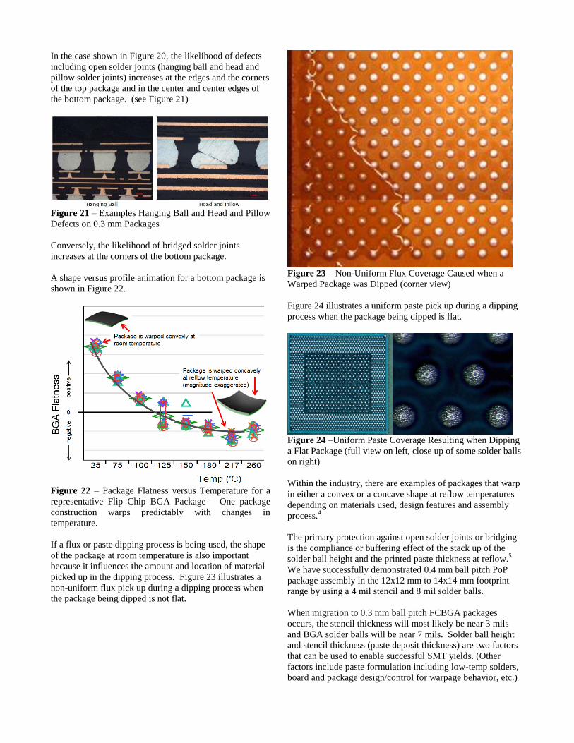
picked up in the dipping process. Figure 23 illustrates a
non-uniform flux pick up during a dipping process when
the package being dipped is not flat.
Figure 23 – Non-Uniform Flux Coverage Caused when a
Warped Package was Dipped (corner view)
Figure 24 illustrates a uniform paste pick up during a dipping
process when the package being dipped is flat.
Figure 24 –Uniform Paste Coverage Resulting when Dipping
a Flat Package (full view on left, close up of some solder balls
on right)
Within the industry, there are examples of packages that warp
in either a convex or a concave shape at reflow temperatures
depending on materials used, design features and assembly
process.4
The primary protection against open solder joints or bridging
is the compliance or buffering effect of the stack up of the
solder ball height and the printed paste thickness at reflow.5
We have successfully demonstrated 0.4 mm ball pitch PoP
package assembly in the 12x12 mm to 14x14 mm footprint
range by using a 4 mil stencil and 8 mil solder balls.
When migration to 0.3 mm ball pitch FCBGA packages
occurs, the stencil thickness will most likely be near 3 mils
and BGA solder balls will be near 7 mils. Solder ball height
and stencil thickness (paste deposit thickness) are two factors
that can be used to enable successful SMT yields. (Other
factors include paste formulation including low-temp solders,
board and package design/control for warpage behavior, etc.)

SECTION 4 – OTHER PROCESSES
Solder Paste Inspection
We conducted a metrology capability analysis of
commonly available solder paste inspection equipment
(about 6 year old technology). Our conclusion was that
these machines are capable of measuring solder paste
prints of 5 mils in diameter and 2 mils thick. This is
significantly smaller than the 7 mils diameter and 3 mils
thick prints that we anticipate are required for 0.3 mm
pitch. Solder paste inspection capability should not be an
issue with any kind of modern machine.
Reflow
There are no anticipated factors where a drop in pitch to
0.3 mm would have any implications to the standard
reflow process.
Rework
Rework of BGAs at 0.3 mm pitch is anticipated to be
much more difficult than 0.4 mm. 0.3 mm pitched rework
is not explored in this paper.
CONCLUSIONS
1. Solder paste printing on complex boards at pitches
below 0.4 mm is not capable with current mainstream
equipment and operation. The impediment is the
inability to get the stencil bottom to mate tightly
against the board surface to enable a consistent and
crisp print. We refer to this as stencil “gasketing”.
Our industry may be able to achieve 0.3 mm pitched
printing with some improvements to the printing
process, particularly with engineered board support
and vacuum fixturing.
2. Assembly yield will become more sensitive to
warpage levels as packages decrease to below 0.4
mm pitch. SMT optimization using smaller solder
balls and thinner paste print at 0.3 mm pitch are
currently less capable to mitigating package warpage.
3. Using generally accepted rules and variance analysis,
solder paste printing machines typically used
throughout our industry should be capable of
achieving X-Y alignment requirements for 0.3 mm
pitched assembly once board support issues have
been fixed.
4. Using generally accepted rules and variance analysis,
placement machines typically used throughout our
industry should be comfortably capable of achieving
X-Y alignment requirements for 0.3 mm pitched
assembly.
5. 0.3 mm pitched assembly will likely require
approximately 3 mil thick stencils with aperture
diameters close to 7 mils.
6. Silkscreen nomenclature on circuit boards with
devices at 0.4 mm pitch is marginally acceptable. At
pitches below 0.4 mm silkscreen nomenclature is not
acceptable.
7. As we move below 0.4 mm pitch, the solder paste powder
size (solder paste type) requirement expected to get finer.
A migration from the typical type 4 paste to type 5 paste
or smaller would give higher average print volume and
tighter print distributions. Type 5 paste looks like the
likely candidate based on printing volume and
consistency at 0.3 mm pitch.
8. Small amounts of stencil cleaning solvents can be
detrimental and cause solder paste bridging at 0.3 mm
pitch. This pitch is much more sensitive to residual
solvent than 0.4 mm and above. Stencil cleaning solvents
should be chosen that evaporate quickly enough to be run
with fine pitches in HVM.
9. The industry standard area ratio rules that ensure good
paste release are still valid at pitches down to 0.3 mm.
Area ratios of about 0.65 and above are still considered to
be safe at 0.3 mm pitch and more aggressive ratios may
be usable if good stencil to board mating is achieved.
10. The relationship between room temperature package
flatness (convex or concave) and reflow temperature
package flatness (convex or concave) should be
understood. This is particularly applicable when the
pitches of devices are 0.4 mm or less. Package flatness
changes with temperature can be significant and vary
widely dependent on each packages unique construction.
AKNOWLEDGEMENTS
I created this paper with the consultation from many others.
Contributors include: Layannah Feller, Lilia May, Andy
Wijaya, Srini Aravamudhan, Prawin Paulraj, Tom Worley,
Dudi Amir, Abhay Watwe, Bill Alger, Gary Brist, Hank
Hsiao, Raiyo Aspandiar, Alan Donaldson, James Wade, J.
Lewis, Todd Harris, Karen Cheng, Dan Burkholder, Mukul
Sakalkale, Doin Davenport, John Schneider, Shawn Lloyd, Ian
Williams, Steve Vandervoort, Gaurang Choksi, Bill Coleman
(Photo Stencil), Sue Holmes (Photo Stencil), Julian Chen
(Shenmao), Tim Jensen (Indium Corporation), Anny Zhang
(Indium Corporation)
REFERENCES
(1) Print Screening Study conducted by Lilia May, Intel
Corporation.
(2) JEDEC standard JESC22-B112A
(3) IPC7095 for SMT defect mitigation techniques
(4) JEDEC standard JEP-95-SPP-024, Table 1 & 2
which includes HT flatness requirements for both
convex and concave packages.
(5) IPC7095 for SMT optimization approaches