Smooth crack-free targets for nuclear applications ... · E-mail address: [email protected] (A....
13
Smooth crack-free targets for nuclear applications produced by molecular plating A. Vascon a,* , S. Santi b , A.A. Isse b , A. Kühnle c , T. Reich a , J. Drebert a , K. Eberhardt a,d , Ch.E. Düllmann a,d,e a Institute of Nuclear Chemistry, Johannes Gutenberg University Mainz, 55099 Mainz, Germany b Department of Chemical Sciences, University of Padova, 35131 Padova, Italy c Institute of Physical Chemistry, Johannes Gutenberg University Mainz, 55099 Mainz, Germany d SHE Chemistry Research Section, Helmholtz Institute Mainz, 55099 Mainz, Germany e SHE Chemistry Department, GSI Helmholtzzentrum für Schwerionenforschung GmbH, 64291 Darmstadt, Germany article info Article history: Received 31 October 2012 Received in revised form 8 February 2013 Accepted 4 March 2013 Available online 14 March 2013 Keywords: Smooth crack-free targets Molecular plating Neodymium γ-ray spectroscopy Atomic force microscopy (AFM) X-ray photoelectron spectroscopy (XPS) abstract The production process of smooth and crack-free targets by means of constant current electrolysis in organic media, commonly known as molecular plating, was optimized. Using a Nd salt, i.e., [Nd(NO 3 ) 3 ·6H 2 O], as model electrolyte several constant current density electrolysis experiments were carried out to investigate the effects of different parameters, namely the plating solvent (isopropanol and isobutanol mixed together, pyridine, and N,N-dimethylformamide), the electrolyte concentration (0.11, 0.22, 0.44mM), the applied current density (0.17, 0.3, 0.7, and 1.3mA/cm 2 ), and the surface roughness of the deposition substrates (12 and 24 nm). Different environments (air and Ar) were used to dry the samples and the effects on the produced layers were investigated. The obtained deposits were characterized using γ-ray spectroscopy for determining Nd deposition yields, X-ray photoelectron spectroscopy for chemical analysis of the produced surfaces, radiographic imaging for surface homo- geneity inspection, atomic force microscopy for surface roughness evaluation, and scanning electron microscopy for surface morphology investigation. The results allowed identifying the optimum para- meters for the production of smooth and crack-free targets by means of molecular plating. The smoothest layers, which had an average RMS roughness of ca. 20 nm and showed no cracks, were obtained using 0.22 mM [Nd(NO 3 ) 3 ·6H 2 O] plated from N,N-dimethylformamide at current densities in the range of 0.3–0.7 mA/cm 2 on the smoothest deposition substrate available. & 2013 Elsevier B.V. All rights reserved. 1. Introduction Targets are an essential component in experimental nuclear science as a source of stationary nuclei, e.g., for atomic and nuclear spectroscopy or nuclear reaction studies [1–3]. Generally, targets should be chemically pure, uniform, homogeneous, crack-free over the area of interest, and well adherent to the deposition substrate. Among the several techniques available to prepare thin layers to be used as nuclear targets [4–8], molecular plating (MP) is one of the most effective and most successfully applied ones [9,10]. This technique, based on the electrodeposition of the element of interest from an organic medium either in the constant current or in the constant voltage mode, is usually chosen because of the possibility to quickly produce deposits of acceptable uniformity and adherence with quantitative yield. Recently Garcia et al. [11,12] applied polymer assisted deposition (PAD), developed by Jia et al. [13] as an alternative method to prepare thin films of metal oxides, to produce nuclear targets. PAD has been claimed to yield targets with better uniformity and homogeneity than MP. In the present work, we demonstrate that thanks to an improved understanding of the electrochemistry of MP and to more extensive surface science investigations [14,15], which showed that the roughness of the films depends on variables like deposition substrate and electrolyte concentration, targets prepared via MP can be also very uniform and homogeneous, as smooth and crack-free layers can be produced. 2. Experiments and results 2.1. Deposition cell The cell used for the MPs is characterized by a central PEEK body where the electrolytic solution is inserted [14]. The anode and the cathode are both Ti blocks covered by a Pd foil and a Ti foil, respectively. Each of the two electrodes has an area of 9 cm 2 . The distance between the electrodes is 2.8 cm. The cathode was designed to be easily removed from the cell and to be used for liquid AFM investigations. Fig. 1 shows the cathode of the cell: a Ti Contents lists available at SciVerse ScienceDirect journal homepage: www.elsevier.com/locate/nima Nuclear Instruments and Methods in Physics Research A 0168-9002/$ - see front matter & 2013 Elsevier B.V. All rights reserved. http://dx.doi.org/10.1016/j.nima.2013.03.003 n Correspondence to: Institute of Nuclear Chemistry, Johannes Gutenberg Uni- versity Mainz, Fritz-Strassmann-Weg 2, D-55128 Mainz, Germany. Tel.: þ49 6131 39 26510; fax: þ49 6131 39 20811. E-mail address: [email protected] (A. Vascon). Nuclear Instruments and Methods in Physics Research A 714 (2013) 163–175
Transcript of Smooth crack-free targets for nuclear applications ... · E-mail address: [email protected] (A....

Nuclear Instruments and Methods in Physics Research A 714 (2013) 163–175
Contents lists available at SciVerse ScienceDirect
Nuclear Instruments and Methods inPhysics Research A
0168-90http://d
n Corrversity39 2651
E-m
journal homepage: www.elsevier.com/locate/nima
Smooth crack-free targets for nuclear applications producedby molecular plating
A. Vascon a,*, S. Santi b, A.A. Isse b, A. Kühnle c, T. Reich a, J. Drebert a, K. Eberhardt a,d, Ch.E. Düllmann a,d,e
a Institute of Nuclear Chemistry, Johannes Gutenberg University Mainz, 55099 Mainz, Germanyb Department of Chemical Sciences, University of Padova, 35131 Padova, Italyc Institute of Physical Chemistry, Johannes Gutenberg University Mainz, 55099 Mainz, Germanyd SHE Chemistry Research Section, Helmholtz Institute Mainz, 55099 Mainz, Germanye SHE Chemistry Department, GSI Helmholtzzentrum für Schwerionenforschung GmbH, 64291 Darmstadt, Germany
a r t i c l e i n f o
Article history:Received 31 October 2012Received in revised form8 February 2013Accepted 4 March 2013Available online 14 March 2013
Keywords:Smooth crack-free targetsMolecular platingNeodymiumγ-ray spectroscopyAtomic force microscopy (AFM)X-ray photoelectron spectroscopy (XPS)
02/$ - see front matter & 2013 Elsevier B.V. Ax.doi.org/10.1016/j.nima.2013.03.003
espondence to: Institute of Nuclear ChemistMainz, Fritz-Strassmann-Weg 2, D-55128 Mai0; fax: þ49 6131 39 20811.ail address: [email protected] (A. Vascon)
a b s t r a c t
The production process of smooth and crack-free targets by means of constant current electrolysisin organic media, commonly known as molecular plating, was optimized. Using a Nd salt, i.e.,[Nd(NO3)3·6H2O], as model electrolyte several constant current density electrolysis experiments werecarried out to investigate the effects of different parameters, namely the plating solvent (isopropanoland isobutanol mixed together, pyridine, and N,N-dimethylformamide), the electrolyte concentration(0.11, 0.22, 0.44 mM), the applied current density (0.17, 0.3, 0.7, and 1.3 mA/cm2), and the surfaceroughness of the deposition substrates (12 and 24 nm). Different environments (air and Ar) were used todry the samples and the effects on the produced layers were investigated. The obtained deposits werecharacterized using γ-ray spectroscopy for determining Nd deposition yields, X-ray photoelectronspectroscopy for chemical analysis of the produced surfaces, radiographic imaging for surface homo-geneity inspection, atomic force microscopy for surface roughness evaluation, and scanning electronmicroscopy for surface morphology investigation. The results allowed identifying the optimum para-meters for the production of smooth and crack-free targets by means of molecular plating. Thesmoothest layers, which had an average RMS roughness of ca. 20 nm and showed no cracks, wereobtained using 0.22 mM [Nd(NO3)3·6H2O] plated from N,N-dimethylformamide at current densities inthe range of 0.3–0.7 mA/cm2 on the smoothest deposition substrate available.
& 2013 Elsevier B.V. All rights reserved.
1. Introduction
Targets are an essential component in experimental nuclearscience as a source of stationary nuclei, e.g., for atomic and nuclearspectroscopy or nuclear reaction studies [1–3]. Generally, targetsshould be chemically pure, uniform, homogeneous, crack-free overthe area of interest, and well adherent to the deposition substrate.Among the several techniques available to prepare thin layers tobe used as nuclear targets [4–8], molecular plating (MP) is one ofthe most effective and most successfully applied ones [9,10]. Thistechnique, based on the electrodeposition of the element ofinterest from an organic medium either in the constant currentor in the constant voltage mode, is usually chosen because of thepossibility to quickly produce deposits of acceptable uniformityand adherence with quantitative yield. Recently Garcia et al. [11,12]applied polymer assisted deposition (PAD), developed by Jia et al.[13] as an alternative method to prepare thin films of metal oxides,
ll rights reserved.
ry, Johannes Gutenberg Uni-nz, Germany. Tel.: þ49 6131
.
to produce nuclear targets. PAD has been claimed to yield targetswith better uniformity and homogeneity than MP. In the presentwork, we demonstrate that thanks to an improved understandingof the electrochemistry of MP and to more extensive surfacescience investigations [14,15], which showed that the roughnessof the films depends on variables like deposition substrate andelectrolyte concentration, targets prepared via MP can be also veryuniform and homogeneous, as smooth and crack-free layers can beproduced.
2. Experiments and results
2.1. Deposition cell
The cell used for the MPs is characterized by a central PEEKbody where the electrolytic solution is inserted [14]. The anodeand the cathode are both Ti blocks covered by a Pd foil and a Ti foil,respectively. Each of the two electrodes has an area of 9 cm2. Thedistance between the electrodes is 2.8 cm. The cathode wasdesigned to be easily removed from the cell and to be used forliquid AFM investigations. Fig. 1 shows the cathode of the cell: a Ti

Ti blockPEEK ring
Ti foil
Fig. 1. 3D drawing of the cathode assembly: a Ti block covered with a circular Ti foilfixed with a PEEK ring. The cathode assembly is part of the molecular plating cell.
Table 1Some physical properties (at 25 °C) of the solvents used for the MPs [16].
Solvent Bp(°C)
Viscosity(cP)
Conductivity(Sm/cm)
Relativepermittivity
Isopropanol (IP) 82.2 2.044 6×10⁻⁸ 19.9Isobutanol (IB) 107.7 3.910 2×10⁻⁸ 17.9Pyridine 115.3 0.884 4×10⁻⁸ 12.9N,N-dimethylformamide(DMF)
153.0 0.802 6×10⁻⁸ 36.7
Table 2Deposition substrates used for the MPs and their average surface roughness values
(RMS) determined by AFM.
Substrate type Production technique RMS (nm)
Ti3 Rolling 24±7Ti5 Magnetron sputtering 12.8±0.7
A. Vascon et al. / Nuclear Instruments and Methods in Physics Research A 714 (2013) 163–175164
block covered with a circular Ti foil fixed with a PEEK ring.A constant temperature of 16 °C was maintained in the cell bywater-cooling the Ti blocks, which were in physical contact withthe electrodes.
2.2. Solvents used for molecular plating
Different solvents were used to perform the MPs: isopropanol,isobutanol, pyridine, and N,N-dimethylformamide (DMF). Isopropanoland isobutanol were always used together as a mixture (3% isopro-panol, 97% isobutanol), hereafter referred to as IPþ IB. Table 1 showssome physical properties of relevance of the used solvents [16].
The data reported in Table 1 show DMF to have the highestboiling point, conductivity, and relative permittivity; its viscosity isinstead the lowest one. Pyridine has the lowest relative permittivity,a viscosity approaching that of DMF and a boiling point quite closeto the one of the IPþ IB mixture. The physical properties of theIPþ IB mixture can be approximated to those of pure isobutanol,which makes up 97% by volume of the mixture. IPþ IB has thehighest viscosity and the lowest conductivity.
2.3. Deposition substrates
The deposition substrates used in the present work are listed inTable 2. Their surface roughnesses, evaluated by AFM (see Section2.5 in [14]) after the cleaning procedure, are reported as averageroot mean square values (RMS). To facilitate comparison of theresults reported here and previously in [14], we keep the labellingof our substrate types as in [14].
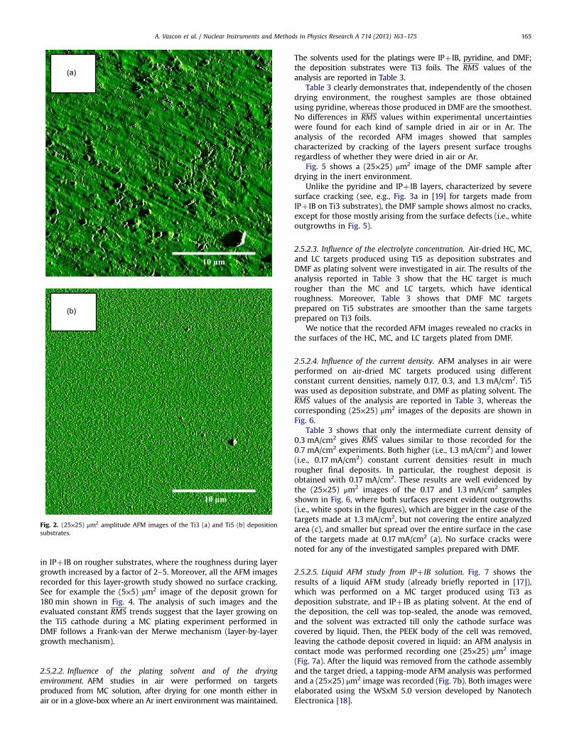
Ti3 was a circular 50 μm-thick Ti foil cut from a bigger foil(Goodfellow). Ti5 was produced by coating a 300-μm thick, mechani-cally polished Si wafer with 100 nm metallic Ti. The substrates usedfor deposition in the cell had different surface roughnesses: larger,corresponding to a more defective surface (Ti3, Fig. 2a), and smaller,corresponding to a less defective surface (Ti5, Fig. 2b).
2.4. Molecular plating at constant current density
Before any deposition, both the anode (Pd foil) and the cathode(Ti foil) were cleaned with 6 M HCl (1×3mL washing), water (3×3mLwashings), and isopropanol (1×3mL washing). Only Ti5 substrateswere cleaned using HCl with a lower concentration (i.e., 0.6 M)in order to avoid corrosion-induced increase in surface roughness, asverified in [14]. For the MPs, 0.338, 0.675, and 1.350 g of[Nd(NO3)3·6H2O] were dissolved in 20 mL 0.1 M HNO3 to give finalsolutions of three different concentrations. From each solution analiquot of 100 μL was added to a mixture of 1 mL isopropanol (FisherChemical) and 34mL isobutanol (Applichem), or to 35 mL of pyridine(Merck) or DMF (Merck), finally yielding three different solutions ofNd3þ in the cell; these are referred to as low concentration(LC, 0.11 mM), medium concentration (MC, 0.22 mM), and highconcentration (HC, 0.44mM). In the cell the concentration of HNO3
was 0.3 mM. The plating solutions were stirred by means of a quartztip ultrasonic stirrer (Bandelin Sonopuls HD 2070) operated at 30%
power pulse. MP experiments were always carried out for 3 h byapplying a constant current of 6 mA, corresponding to a currentdensity of 0.7 mA/cm2. Three-hours long MPs were also performedby testing different constant currents, i.e., 1.5, 3, or 12 mA. Thecorresponding current densities were 0.17, 0.3, and 1.3 mA/cm2
(Table 3).
2.5. Atomic force microscopy (AFM) studies
2.5.1. ExperimentsThe surface roughness of the deposited layers, i.e., the measure
of the texture of a surface quantified by the vertical deviations of areal surface from its ideal planar form, was investigated by usingatomic force microscopy (AFM) (MFP 3D Asylum Research). AFMinvestigations were performed in air and in liquid.
The tapping-mode AFM analysis in air was the same for all theproduced targets: ten (5×5) μm2 and one (25×25) μm2 images wererecorded for each target. From each of the ten (5×5) μm2 images tworoot mean square (RMS) values were evaluated using a (1.5×1.5) μm2
mask in two different positions inside the image. From each of the(25×25) μm2 images, twenty RMS values were evaluated using(1.5×1.5) μm2 masks in twenty different positions of the image. Inthe case of samples presenting surfaces with cracks, the masks wereused only in the crack-free areas, as the cracks do not belong to thesurface and hence do not define the real roughness of the depositedlayers. The final surface roughness value of each of the image sizeswas evaluated for each target as the arithmetic mean of all the RMSvalues measured for that specific image size (i.e., RMS).
2.5.2. Results2.5.2.1. Layer-growth studies from DMF solution. The growthmechanism of the layers was studied as a function of platingtime by measuring the RMS of air-dried targets. Twelve targetswere produced using different deposition times: the first targetwas produced after 15 min plating and the subsequent ones afterincrements of 15 min up to 180 min. The targets were preparedusing a 0.22 mM Nd salt (i.e., MC), Ti5 deposition substrates, at acurrent density of 0.7 mA/cm2, and DMF as plating solvent. Thegrowth study was restricted to DMF because it showed verypromising results, as we briefly reported in [17] where somepreliminary tests with this solvent were described.
In Fig. 3 the RMS trends of the growing layer show an almostconstant behaviour (average value ca. 14 nm) during the wholeperiod of deposition (3 h): the surface roughness does not undergomajor variations. This is in contrast to similar studies performed
10 μm
10 μm
Fig. 2. (25×25) μm2 amplitude AFM images of the Ti3 (a) and Ti5 (b) depositionsubstrates.
A. Vascon et al. / Nuclear Instruments and Methods in Physics Research A 714 (2013) 163–175 165
in IPþ IB on rougher substrates, where the roughness during layergrowth increased by a factor of 2–5. Moreover, all the AFM imagesrecorded for this layer-growth study showed no surface cracking.See for example the (5×5) μm2 image of the deposit grown for180 min shown in Fig. 4. The analysis of such images and theevaluated constant RMS trends suggest that the layer growing onthe Ti5 cathode during a MC plating experiment performed inDMF follows a Frank-van der Merwe mechanism (layer-by-layergrowth mechanism).
2.5.2.2. Influence of the plating solvent and of the dryingenvironment. AFM studies in air were performed on targetsproduced from MC solution, after drying for one month either inair or in a glove-box where an Ar inert environment was maintained.
The solvents used for the platings were IPþ IB, pyridine, and DMF;the deposition substrates were Ti3 foils. The RMS values of theanalysis are reported in Table 3.
Table 3 clearly demonstrates that, independently of the chosendrying environment, the roughest samples are those obtainedusing pyridine, whereas those produced in DMF are the smoothest.No differences in RMS values within experimental uncertaintieswere found for each kind of sample dried in air or in Ar. Theanalysis of the recorded AFM images showed that samplescharacterized by cracking of the layers present surface troughsregardless of whether they were dried in air or Ar.
Fig. 5 shows a (25×25) μm2 image of the DMF sample afterdrying in the inert environment.
Unlike the pyridine and IPþ IB layers, characterized by severesurface cracking (see, e.g., Fig. 3a in [19] for targets made fromIPþ IB on Ti3 substrates), the DMF sample shows almost no cracks,except for those mostly arising from the surface defects (i.e., whiteoutgrowths in Fig. 5).
2.5.2.3. Influence of the electrolyte concentration. Air-dried HC, MC,and LC targets produced using Ti5 as deposition substrates andDMF as plating solvent were investigated in air. The results of theanalysis reported in Table 3 show that the HC target is muchrougher than the MC and LC targets, which have identicalroughness. Moreover, Table 3 shows that DMF MC targetsprepared on Ti5 substrates are smoother than the same targetsprepared on Ti3 foils.
We notice that the recorded AFM images revealed no cracks inthe surfaces of the HC, MC, and LC targets plated from DMF.
2.5.2.4. Influence of the current density. AFM analyses in air wereperformed on air-dried MC targets produced using differentconstant current densities, namely 0.17, 0.3, and 1.3 mA/cm2. Ti5was used as deposition substrate, and DMF as plating solvent. TheRMS values of the analysis are reported in Table 3, whereas thecorresponding (25×25) μm2 images of the deposits are shown inFig. 6.
Table 3 shows that only the intermediate current density of0.3 mA/cm2 gives RMS values similar to those recorded for the0.7 mA/cm2 experiments. Both higher (i.e., 1.3 mA/cm2) and lower(i.e., 0.17 mA/cm2) constant current densities result in muchrougher final deposits. In particular, the roughest deposit isobtained with 0.17 mA/cm2. These results are well evidenced bythe (25×25) μm2 images of the 0.17 and 1.3 mA/cm2 samplesshown in Fig. 6, where both surfaces present evident outgrowths(i.e., white spots in the figures), which are bigger in the case of thetargets made at 1.3 mA/cm2, but not covering the entire analyzedarea (c), and smaller but spread over the entire surface in the caseof the targets made at 0.17 mA/cm2 (a). No surface cracks werenoted for any of the investigated samples prepared with DMF.
2.5.2.5. Liquid AFM study from IPþ IB solution. Fig. 7 shows theresults of a liquid AFM study (already briefly reported in [17]),which was performed on a MC target produced using Ti3 asdeposition substrate, and IPþ IB as plating solvent. At the end ofthe deposition, the cell was top-sealed, the anode was removed,and the solvent was extracted till only the cathode surface wascovered by liquid. Then, the PEEK body of the cell was removed,leaving the cathode deposit covered in liquid: an AFM analysis incontact mode was performed recording one (25×25) μm2 image(Fig. 7a). After the liquid was removed from the cathode assemblyand the target dried, a tapping-mode AFM analysis was performedand a (25×25) μm2 image was recorded (Fig. 7b). Both images wereelaborated using the WSxM 5.0 version developed by NanotechElectronica [18].

Table 3Overview of relevant molecular plating parameters. Average root mean square (RMS) values obtained from the AFM analyses of the samples investigating the influence ofplating solvent, drying environment, electrolyte concentration, and current density on the surface roughness of the produced layers.
Substrate type Solvent Drying environment Concentration Current density (mA/cm2) Scan size (μm2) RMS (nm)
Ti3 Pyridine Air MC 0.7 (5×5) 242±140(25×25) 372±190
Ti3 Pyridine Ar MC 0.7 (5×5) 320±160(25×25) 350±180
Ti3 IPþ IB Air MC 0.7 (5×5) 150±40(25×25) 190±70
Ti3 IPþ IB Ar MC 0.7 (5×5) 140±60(25×25) 180±80
Ti3 DMF Air MC 0.7 (5×5) 61±24(25×25) 130±40
Ti3 DMF Ar MC 0.7 (5×5) 52±23(25×25) 110±50
Ti5 DMF Air HC 0.7 (5×5) 70±21(25×25) 79±14
Ti5 DMF Air MC 0.7 (5×5) 17±8(25×25) 18±9
Ti5 DMF Air LC 0.7 (5×5) 17±3(25×25) 18±8
Ti5 DMF Air MC 0.17 (5×5) 110±35(25×25) 130±25
Ti5 DMF Air MC 0.3 (5×5) 10±4(25×25) 12±5
Ti5 DMF Air MC 1.3 (5×5) 70±30(25×25) 80±22
RMS (5 × 5 μm2)
RMS (25 × 25 μm2)
Fig. 3. RMS vs. time trend of the layer-growth study of the air-dried targetsproduced using 0.22 mM Nd salt with DMF and Ti5 deposition substrates.
2
A. Vascon et al. / Nuclear Instruments and Methods in Physics Research A 714 (2013) 163–175166
The 3D AFM images of Fig. 7 indicate that the cracking of thesurfaces develops after the removal of the liquid and the drying ofthe deposited layer.
Fig. 4. Layer-growth studies from DMF solution. (5×5) μm topography AFM imageof the sample plated for 180 min using Ti5 substrate and MC plating solutionin DMF.
2.6. Scanning electron microscopy (SEM) studies
2.6.1. ExperimentsThe morphology of the targets was studied using scanning
electron microscopy (SEM) (Philips XL30). The microscope wasoperated at 20 kV. The pressure inside the vacuum chamberwas 5 mPa. Backscattered and secondary electrons were detected.A magnification factor of 1000× was used.
2.6.2. ResultsFig. 8 shows 1000× SEM images of three MC samples produced
using the following deposition substrates and plating solvents: (a) Ti3and pyridine, (b) Ti3 and DMF, (c) Ti5 and DMF. All samples were air-dried. Among the several SEM images recorded, these particular ones
were chosen for display here because of the important surfacemorphology information they convey.
Fig. 8a shows a large-area image of an air-dried pyridine MCtarget. The surface of the sample suffers from severe cracking andit is visibly rough.
Figs. 8b and c show an important effect of the depositionsubstrate (Ti3 vs. Ti5) on the surface morphology of the deposits.These images indicate that MC targets prepared using DMF and aTi3 substrate (Fig. 8b) exhibit cracks in the layer, caused mainly bythe grown surface defects, as already shown in Fig. 5. If, instead, asmoother deposition substrate is used, i.e., Ti5, MC targets pro-duced using DMF (Fig. 8c) show no surface cracks (see also Fig. 4).In contrast, MC experiments using IPþ IB (see Fig. 2b in [14])
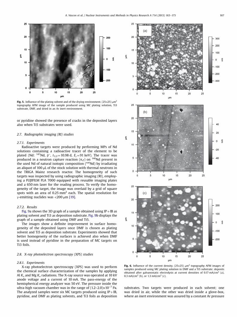
Fig. 5. Influence of the plating solvent and of the drying environment. (25×25) μm2
topography AFM image of the sample produced using MC plating solution, Ti3substrate, DMF, and dried in an Ar inert environment.
Fig. 6. Influence of the current density. (25×25) μm2 topography AFM images ofsamples produced using MC plating solution in DMF and a Ti5 substrate; depositsobtained after galvanostatic electrolysis at current densities of 0.17 mA/cm2 (a),0.3 mA/cm2 (b), or 1.3 mA/cm2 (c).
A. Vascon et al. / Nuclear Instruments and Methods in Physics Research A 714 (2013) 163–175 167
or pyridine showed the presence of cracks in the deposited layersalso when Ti5 substrates were used.
2.7. Radiographic imaging (RI) studies
2.7.1. ExperimentsRadioactive targets were produced by performing MPs of Nd
solutions containing a radioactive tracer of the element to beplated (Nd: 147Nd, β−, t1/2¼10.98 d, Eγ¼91 keV). The tracer wasproduced in a neutron capture reaction (n,γ) on 146Nd present inthe used Nd of natural isotopic composition (natNd) by irradiatingan aliquot of 100 μL of the stock solution with thermal neutrons inthe TRIGA Mainz research reactor. The homogeneity of suchtargets was inspected by using radiographic imaging (RI), employ-ing a FUJIFILM FLA 7000 equipped with reusable imaging platesand a 650 nm laser for the reading process. To verify the homo-geneity of the target, the image was overlaid by a grid of squarespots with an area of 0.25 mm2 each. The spatial resolution forγ-emitting nuclides was <200 μm [19].
2.7.2. ResultsFig. 9a shows the 3D graph of a sample obtained using IPþ IB as
plating solvent and Ti3 as deposition substrate. Fig. 9b displays thegraph of a sample obtained using DMF and Ti5.
The images show a definite improvement in surface homo-geneity of the deposited layers once DMF is chosen as platingsolvent and Ti5 as deposition substrate. Experiments showed thatbetter homogeneity of the surfaces is achieved also when DMFis used instead of pyridine in the preparation of MC targets onTi3 foils.
2.8. X-ray photoelectron spectroscopy (XPS) studies
2.8.1. ExperimentsX-ray photoelectron spectroscopy (XPS) was used to perform
the chemical surface characterization of the samples by applyingAl Kα and Mg Kα radiations. The X-ray source was operated at 10 kVanode voltage and a current of 10 mA. The pass-energy of thehemispherical energy analyzer was 50 eV. The pressure inside theultra-high vacuum chamber was in the range of (1.2–2.0)×10−7 Pa.The analyzed samples were six MC targets produced using IPþ IB,pyridine, and DMF as plating solvents, and Ti3 foils as deposition
substrates. Two targets were produced in each solvent; onewas dried in air, while the other was dried inside a glove-box,where an inert environment was assured by a constant Ar pressure

Fig. 7. Liquid AFM study from IPþ IB solution. 3D (25×25) μm2 topography AFMimages of the target produced using Ti3 and MC plating solution in IPþ IB before(a) and after solvent removal and drying (b).
Fig. 8. Influence of substrate surface roughness and plating solvent. 1000× SEMimages of the air-dried samples produced using MC plating solution and thefollowing substrate/solvent systems: (a) Ti3/pyridine, (b) Ti3/DMF, (c) Ti5/DMF.
A. Vascon et al. / Nuclear Instruments and Methods in Physics Research A 714 (2013) 163–175168
(50 Pa below atmospheric pressure, O2<1 ppm, H2O<1 ppm). Werefer to [14] for details about the drying procedure in an inertenvironment and the subsequent XPS analysis. Drying in differentenvironments was investigated to probe whether reactive or inertenvironments like, respectively, air or Ar cause different surfacechemical reactions to take place, the products of which might beidentified by XPS.
After the first surface investigation, the samples underwent10 min sputtering using 4 kV Arþ ions, followed by further XPSanalysis.
The binding energies of the XPS lines of interest were deter-mined by fitting the recorded XPS spectra. The analyses wereperformed using the CasaXPS software (version 2.3.15), withwhich the background was subtracted adopting the Shirley
algorithm, and the peaks were fitted using the Gaussian/Lorent-zian product formula. As the aim of the present work was mainlyto investigate the surface chemistry of the samples after drying indifferent environments, a detailed chemical surface analysis of the

0
34 mm
34 mm
0
34 mm
34 mm
Fig. 9. Influence of substrate surface roughness and plating solvent. RI 3D graphs ofsamples produced using MC plating solution and the following substrate/solventsystems: (a) Ti3/IPþ IB, (b) Ti5/DMF.
A. Vascon et al. / Nuclear Instruments and Methods in Physics Research A 714 (2013) 163–175 169
deposits was performed only for C, which was known from [14]to be the main element composing the outer layer of the producedsamples. The C 1s spectra are therefore the only ones to be shownwith multicomponent fitting analysis, which was always modelledby fixing the separations in binding energy, the intensity ratios,and the full widths at half maxima (FWHM) of the different C 1scomponents of IPþ IB, DMF, and pyridine. For the IPþ IB and DMFsamples dried both in air and in Ar environment, the analysisbefore sputtering required correcting the binding energies for thesurface charging using one of the components of the C 1s lines: the284.9 eV component [20] for IPþ IB, and the 285.8 eV component[21] for DMF. After sputtering, the imprecise fittings of thereference C 1s peaks required the use of a higher binding energypeak (ca. 289 eV) present in the same C 1s spectra to correct forthe surface charge effect. For the air- and Ar-dried pyridinesamples, instead, the correction of the binding energies wasperformed both before and after sputtering using the intenseN 1s line of pyridine at 400.2 eV [22]. The experimental uncer-tainty of the binding energies is ±0.1 eV.
2.8.2. ResultsThe XPS analyses of the six MC targets never showed the presence
of Ti signals, indicating that all the deposited layers are thick.The Nd analysis of the samples required the use of Mg Kα
radiation to avoid an interference with the Auger lines of oxygen in
the binding energy region of Nd 3d. The Nd 3d spectra of all thesamples dried in Ar environment (not shown) were identical tothose of the air-dried targets, except for smaller intensities of therecorded peaks.
Differences among the recorded XPS signals of the IPþ IB, DMFand pyridine spectra were noted only for the C 1s lines of the air-and Ar-dried samples.
2.8.2.1. Samples prepared from IPþ IB. The XPS analyses of the air-and Ar-dried IPþ IB samples showed the presence of the followingelements: C, O, Pd, and Nd. The corresponding XPS signals were:C 1s, O 1s, Pd 3d, Nd 3d, and Nd 4d. Fig. 10 shows the spectra of Nd3d (a) and C 1s (b) of the sample dried in air and Fig. 10c the C 1sspectra of the sample dried in Ar environment. The model appliedfor the multicomponent fitting analysis of the C 1s peaks took intoaccount only the C 1s components of isobutanol, as isopropanolcorresponds to just 3% of the total volume of the solvent.According to literature [20], the C 1s components of isobutanolhave binding energies at 284.9 eV, 285.0 eV, and 286.5 eV, with anintensity ratio of 2:1:1. Table 4 shows the ratios of the total peakareas C 1s/Nd 3d, O 1s/C 1s, and the ratios between the sum of thepeaks fitting a certain spectral component and a total peak area,like the ratios reported as C 1s (ca. 285 eV)/Nd 3d, C 1s (ca.286 eV)/Nd 3d, and C 1s (ca. 289 eV)/Nd 3d. The ratios wereevaluated before and after 10 min sputtering.
The measured binding energy of the Nd 3d5/2 peak is 982.8 eV(Fig. 10a) and can be compared to the literature value of 983.1 eV[23] for Nd3þ . This indicates that Nd is present as Nd3þ in thedeposited layer (possibly as carboxylate, oxide, or hydroxide) [14].
The C 1s spectra reported in Figs. 10b and c show the presenceof two components: the C 1s peaks at ca. 285.0 eV, whichremarkably decrease upon Arþ sputtering, are due to physisorbedaliphatic carbon of the mixed isopropanol/isobutanol solvent. Thepeaks at the higher binding energy (i.e., 289.9 and 289.6 eV for air-and Ar-dried samples, respectively) can be attributed, according toliterature, to COOM – metal carboxylate – (289.0 eV [23]) groupsformed during the plating process, which are chemisorbed, asfollows from the observation that they are not easily removed bythe sputtering. This shows that the solvent undergoes electrolysisduring the MP process and becomes oxidized.
For a more detailed analysis of the Nd 3d and C 1s spectra of theIPþ IB samples we refer to [14].
The spectra of Fig. 10, as well as the C 1s/Nd 3d ratios reportedin Table 4, show that for both air- and Ar-dried samples theintensity of the Nd 3d signal increases, while that of C 1s decreaseswhen the surface is sputtered with Arþ for 10 min. This resultshows that the Nd deposit is covered with a layer of solvent.
A consequence of drying the samples in air can be inferred fromthe different intensity ratios of the two C 1s components at 0 minsputtering in Figs. 10b and c: the 1:1 ratio of the Ar-dried samplebecomes almost 1:2 after drying in air. From the analysis of theC 1s (ca. 285 eV)/Nd 3d and C 1s (ca. 289 eV)/Nd 3d ratios it isevident that while the intensity of the chemisorbed C 1s (ca.289 eV) component is not affected by the method of drying, thephysisorbed one (ca. 285.0 eV) decreases when the sample is driedin air. As a consequence more intense Nd 3d signals, hence smallerC/Nd ratios (see Table 4), are recorded for the air-dried sample.
2.8.2.2. Samples prepared from DMF. As regards the XPS analyses ofthe targets prepared in DMF, the spectra of both air- and Ar-driedsamples showed the presence of the following elements: C, N, O,and Nd. The corresponding XPS signals were: C 1s, N 1s, O 1s, Nd3d, and Nd 4d. No signals of Pd were detected. Fig. 11 shows thespectra of Nd 3d (a) and C 1s (b) of the sample dried in air, andFig. 11c the C 1s spectra of the sample dried in Ar environment.

Table 4Ratios of the peak areas of some of the detected elements before and after 10 minsputtering.
Sample Ratios of XPSpeak areas
Air Ar
0 minsputtering
10 minsputtering
0 minsputtering
10 minsputtering
IPþIB C 1s/Nd 3d 0.04 0.015 0.11 0.020O 1s/C 1s 6 10 4 9C 1s (ca.285 eV)/Nd 3d
0.014 0.0026 0.05 0.008
C 1s (ca.289 eV)/Nd 3d
0.026 0.012 0.04 0.011
DMF C 1s/Nd 3d 0.05 0.011 0.10 0.014O 1s/C 1s 6 15 5 12C 1s (ca.286 eV)/Nd 3d
0.022 0.0018 0.07 0.005
C 1s (ca.289 eV)/Nd 3d
0.03 0.009 0.028 0.009
Pyridine C 1s/Nd 3d 0.9 0.14 1.1 0.20O 1s/C 1s 1.3 1.4 1.2 1.4C 1s (ca.286 eV)/Nd 3d
0.8 0.13 1.0 0.17
C 1s (ca.289 eV)/Nd 3d
0.10 0.015 0.12 0.021
Fig. 10. XPS spectra of samples obtained after plating on Ti3 substrates using MCplating solution in IPþ IB: (a) Nd 3d (air-dried), (b) C 1s (air-dried), and (c) C 1s(Ar-dried) before sputtering (indicated as 0 min sputtering in the figure), and after10 min sputtering with Arþ ions. Offsets were applied for clarity.
A. Vascon et al. / Nuclear Instruments and Methods in Physics Research A 714 (2013) 163–175170
According to literature [21], the C 1s components of DMF havebinding energies at 285.8 eV, and 288.8 eV with an intensity ratioof 2:1.
The XPS spectra of the DMF samples (Fig. 11) are quite similarto those of the IPþ IB samples (Fig. 10). The measured bindingenergy of the Nd 3d5/2 peak (i.e., 983.6 eV, Fig. 11a) confirms thatNd is deposited as Nd3þ also in DMF (possibly as carboxylate,oxide, or hydroxide). The C 1s spectra reported in Figs. 11b and cshow again the presence of two components: the components ofthe physisorbed solvent at ca. 286 eV and 289 eV, and thecomponents of chemisorbed species at 290.2 eV in air, and at289.4 eV in Ar environment. As in the case of IPþ IB, the C 1s peakof the chemisorbed species can be attributed to possible COOM –
metal carboxylate – groups formed during the plating process. Theproduced samples are again characterized by an outer layer ofsolvent which covers the Nd deposit, as indicated by the spectra ofFig. 11, as well as by the ratios C 1s/Nd 3d reported in Table 4.These ratios show that, for both air- and Ar-dried samples, theintensity of the Nd 3d signal increases with sputtering time, whilethat of C 1s decreases.
As in the case of MPs in IPþ IB, the difference between drying inair or Ar is reflected by the smaller C 1s/Nd 3d ratio in air than inAr, i.e., 0.05 instead of 0.10 (Table 4). This difference is alsoconfirmed by the larger value of the C 1s (ca. 286 eV)/Nd 3d ratioin Ar than in air. Therefore, also in the case of DMF, the 1:1 ratio ofthe C 1s signals of the Ar-dried sample becomes almost 1:2 afterdrying in air. The C 1s (ca. 289 eV)/Nd 3d ratios are very similarboth in air and in Ar, indicating that the chemisorbed products arenot considerably affected by drying in different environments.
2.8.2.3. Samples prepared from pyridine. The XPS analyses of theair- and Ar-dried pyridine samples showed the presence of thefollowing elements: C, N, O, Pd, and Nd. The corresponding XPSsignals were: C 1s, N 1s, O 1s, Pd 3d, Nd 3d, and Nd 4d. Fig. 12shows the spectra of Nd 3d (a) and C 1s (b) of the sample dried inair, and Fig. 12c the C 1s spectra of the sample dried in Arenvironment. According to literature [22], the C 1s components ofpyridine have binding energies at 285.5 eV, 285.9 eV, and 286.3 eV,with an intensity ratio of 2:1:2.
The spectra of Fig. 12a show that the Nd 3d signal beforesputtering is quite low. It is much lower than the Nd 3d signals ofthe corresponding (unsputtered) IPþ IB and DMF samples

Fig. 11. XPS spectra of samples obtained after plating on Ti3 substrates using MCplating solution in DMF: (a) Nd 3d (air-dried), (b) C 1s (air-dried), and (c) C 1s(Ar-dried) before sputtering (indicated as 0 min sputtering in the figure), and after10 min sputtering with Arþ ions. Offsets were applied for clarity.
295
295
air-dried
air-dried
Ar-dried
970 980 990 1000 1010
× 103
70
60
50
40
30
× 103
25
20
15
10
5
× 103
25
20
15
10
5
280 285 290
280 285 290
Fig. 12. XPS spectra of samples obtained after plating on Ti3 substrates using MCplating solution in pyridine: (a) Nd 3d (air-dried), (b) C 1s (air-dried), and (c) C 1s(Ar-dried) before sputtering (indicated as 0 min sputtering in the figure), and after10 min sputtering with Arþ ions. Offsets were applied for clarity.
A. Vascon et al. / Nuclear Instruments and Methods in Physics Research A 714 (2013) 163–175 171
DMF
IP+IB
Fig. 13. Cell potential vs. time curves of molecular platings on Ti3 foils performedusing MC plating solution in DMF (a) or IPþ IB (b), and applying a constant currentof 6 mA (current density 0.7 mA/cm2).
A. Vascon et al. / Nuclear Instruments and Methods in Physics Research A 714 (2013) 163–175172
(compare Fig. 12a with Figs. 10a and 11a). As shown by Fig. 12a andby the C 1s/Nd 3d ratios reported in Table 4, the intensity of theNd 3d signal increases considerably after 10 min sputtering withArþ ions. Therefore, the produced sample is characterized by athicker solvent layer covering the deposit compared to IPþ IB andDMF. The measured binding energy of the Nd 3d5/2 peak (i.e.,983.4 eV, Fig. 12a) confirms that Nd is deposited as Nd3þ aspreviously found in the case of IPþ IB and DMF (possibly ascarboxylate, oxide, or hydroxide). The C 1s spectra reported inFigs. 12b and c show the presence of two components, which arevisible only after multicomponent fitting analysis: the componentsof physisorbed pyridine at ca. 286 eV, and the components ofchemisorbed species at ca. 289 eV (i.e., air: 289.3 eV, Ar: 289.4 eV).These higher binding energy components can be attributed topossible COOM – metal carboxylate – groups formed during theplating process. This indicates that the solvent undergoes electro-lysis during the MP process and becomes oxidized. Nonetheless,the very small intensities of the chemisorbed components suggestthat pyridine undergoes electrolysis only to a smaller degree thanIPþ IB or DMF.
Slight differences between drying in air or Ar are shown by thesmaller C 1s/Nd 3d ratio in air (i.e., 0.9 instead of 1.1), and by thelarger value of the C 1s (ca. 286 eV)/Nd 3d ratio in Ar than in air.These differences are smaller than in the case of IPþ IB and DMF.The C 1s (ca. 289 eV)/Nd 3d ratios are very similar both in air andin the Ar environment.
It has to be noticed that all the values of the ratios reported inTable 4 for the deposits prepared in pyridine are quite differentfrom the corresponding values determined for IPþ IB or DMFdeposits, irrespective of the methods of sample drying. Thisfollows from the large intensities of the C 1s signals in pyridine,as evidenced by the C 1s spectra reported in Figs. 12b and c, whereeven after 10 min sputtering the intensities of the physisorbedcomponents are only slightly decreased.
The comparisons between the C 1s spectra in Figs. 10b, c, 11b, cand 12b, c show no chemical shifts before and after sputtering.Small shifts of ca. −0.5 eV after sputtering were observed for theNd 3d spectra of the IPþ IB and DMF samples (see Fig. 10a forIPþ IB, and Fig. 11a for DMF). Shifts of ca. þ0.5 eV after sputteringwere observed for the Nd 3d spectra of the pyridine samples (seeFig. 12a). This could indicate the presence of different Nd3þ speciesin the topmost surface layers of the samples produced from thedifferent solvents.
From the analysis of all the obtained XPS results, the maindifference which appears to occur between samples dried in airand in a controlled inert environment, such as Ar in a glove-box, isrelated to the higher intensities of the peaks of the physisorbedsolvent components when the drying is performed in Ar. Besidesthis, a slightly larger amount of O adsorbed on the surfaces ofall the samples dried in air can be noticed (see O 1s/C 1s ratios inTable 4). Nonetheless, no strong indication for the presence ofsurface chemical reaction products promoted by the drying in airinstead of Ar was found.
2.9. Molecular plating from DMF solution
2.9.1. Cell potential trendsFig. 13 shows trends of cell potential vs. time recorded during
preparation of targets, using 0.22 mM [Nd(NO3)3·6H2O] solution(MC), Ti3 as deposition foil, and DMF (a) or IPþ IB (b) as platingsolvent. The applied constant current was 6 mA for 3 h (currentdensity 0.7 mA/cm2). IPþ IB cell potential curves were alreadydiscussed in detail in [14].
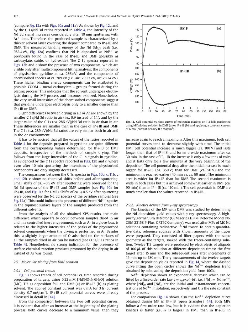
From the comparison between the two cell potential curves,it is evident that after an increase at the beginning of the platingprocess, both curves decrease to a minimum value, then they
increase again to reach a maximum. After this maximum, both cellpotential curves tend to decrease slightly with time. The initialDMF cell potential increase is much bigger (ca. 100 V) and lastslonger than that of IPþ IB, and forms a wide maximum after ca.30 min. In the case of IPþ IB the increase is only a few tens of voltsand it lasts only for a few minutes at the very beginning of thedeposition. The cell potential drop after the initial increase is muchbigger for IPþ IB (ca. 350 V) than for DMF (ca. 50 V) and theminimum is reached earlier (45 min vs. ca. 60 min). The minimumarea is wider for IPþ IB than for DMF. The second maximum iswide in both cases but it is achieved somewhat earlier in DMF (ca.90 min) than in IPþ IB (ca. 110 min). The cell potentials in DMF aremuch smaller than the values recorded in IPþ IB.
2.9.2. Kinetics derived from γ-ray spectroscopyThe kinetics of the MP with DMF was studied by determining
the Nd deposition yield values with γ-ray spectroscopy. A high-purity germanium detector (GEM series HPGe Detector Model No.GEM 23158 P-Plus, ORTEC Company), was used after MPs of MC Ndsolutions containing radioactive 147Nd tracer. To obtain quantita-tive data, reference sources with known amounts of the tracerwere prepared. They consisted of filter papers with the samegeometry as the targets, soaked with the tracer-containing solu-tion. Twelve Ti3 targets were produced by electrolysis of aliquotsof 100 μL of this solution at different deposition times: the firsttarget after 15 min and the subsequent ones after increments of15 min up to 180 min. The γ-measurements of the twelve targetsgave the deposition yields reported in Fig. 14, where the dashedcurve fitting the open circles shows the Nd3þ depletion trendobtained by subtracting the deposition yield from 100%.
Nd3þ depletion shows an exponential decrease which can befitted by a first-order rate law y¼ y0expð−btÞ, i.e., [Nd]t¼[Nd]0e−kt,where [Nd]0 and [Nd]t are the initial and instantaneous concen-trations of Nd3þ in solution, respectively, and k is the rate constantof the process.
For comparison Fig. 14 shows also the Nd3þ depletion curveobtained during MP in IPþ IB (open triangles) [14]. Both MPsfollow a first-order rate law, but it is evident that the depletionkinetics is faster (i.e., k is larger) in DMF than in IPþ IB. In

Fig. 14. Molecular platings on Ti3 foils performed using MC plating solution in DMFor IPþ IB: Nd3þ deposition yield (open squares) and depletion rate (open circles) inDMF, depletion rate in IPþ IB [14] (open triangles); the lines are best fittingsaccording to a first-order growth or decay. Error bars are not shown as smaller thanthe size of the symbols.
A. Vascon et al. / Nuclear Instruments and Methods in Physics Research A 714 (2013) 163–175 173
particular, it is important to notice that, as in the case of IPþ IB[14], the MP in DMF reaches an almost complete depletion of theNd ions at a time corresponding to the recorded minimum (i.e., ca.60 min) of the cell potential curve.
2.9.3. Conductivity measurementsThe conductivity was measured using an inoLab Cond 720
conductometer connected to a TetraCon 325 standard conductivitycell. These measurements were performed only in a stirred DMFsolution containing 0.22 mM [Nd(NO3)3·6H2O] and 0.3 mM HNO3.The conductivity (χ) was measured to be 46.5±0.1 μS/cm. Thisvalue was used to evaluate the solution resistance, R, in the cell.The expression used for this evaluation is R¼ρ.l/S [24], where ρ isthe resistivity of the system (i.e., the inverse of the conductivity,ρ¼21.50±0.05 kΩ/cm), l is the distance between the electrodes(2.80±0.01 cm), and S is the surface area of the electrodes (9.0±0.1 cm2). The obtained cell resistance is 6.691±0.011 kΩ. UsingOhm's first law, V¼RI, where R is the cell resistance and I is theapplied current (I¼6.00±0.01 mA), the contribution of the ohmicdrop to the overall cell potential was estimated to 40.15±0.09 V.This value is in perfect agreement with the initial experimentalvalue in Fig. 13a. The cell potential during the MP process is,however, at least twice as high as the initial value. The voltageincrease during the first 15 min of the electroplating is probablydue to an increase of the overall resistance of the cell. Indeed,during MP the concentration of the electrolyte decreases as Nd3þ
is deposited on the cathode, resulting in a decrease of conductivity.Also the formation and growth of the deposit, which is principallycomposed of Nd salts and complexes, presents an additionalresistance. It appears reasonable that the cell potential observedduring MPs is dominated by the ohmic drop.
2.9.4. Temperature measurementsTemperature measurements of the DMF plating solutions were
performed using a TFK 150 thermometer connected to an inoLabpH 720 pH meter. The temperature was measured immediatelybefore and after 3 h constant current density MP experiments at0.17, 0.3 and 1.3 mA/cm2. In all cases the MP experiments startedafter the solutions were cooled down to 16 °C. The measurementsshowed temperature increases of 0.4±0.1 1C, 0.7±0.1 1C, and 2.0±0.1 °C, respectively. These results indicate that despite constantcooling during the experiments, a higher current density leads to amore pronounced temperature increase inside the system.
3. Discussion
Among various experimental parameters that may affect con-stant current density MP, two were found to be of crucialimportance for the preparation of smooth and crack-free layersto be used as nuclear targets. These are the roughness of thedeposition substrate and the solvent used for the platings. Thedifferent RMS values of the DMF MC targets grown on Ti3 and Ti5substrates confirm that even small differences in surface rough-ness between the deposition substrates can influence the RMS ofthe growing layers [14]. Indeed, if the deposition substrate is rough(i.e., defective), the surface mobility of the deposited atoms will bereduced by trapping in the defects, and the produced layer will beof very low quality. Therefore, to produce smooth targets, deposi-tion substrates as smooth as possible are required.
As regards the solvent, its importance does not only derivefrom being the medium in which the process is performed andhence the major factor influencing the electrochemistry of the MP,but also from the fact that the produced layers are mainlycomposed of physisorbed as well as chemisorbed solvent mole-cules. Hence, the role of the solvent in MP is twofold: it influencesthe electrochemistry of the process, but also the properties of thelayer to be produced. Reasonable physical properties to be takeninto account when choosing a solvent for MP are boiling point,viscosity, conductivity, and relative permittivity [16]. The boilingpoint determines the volatility of the solvent. The viscosityinfluences the rate of mass transfer in the solvent and is importantin mass-transport controlled electrolytic processes like MP [14].In turn, the rate of mass transfer influences the conductivity of theelectrolyte solutions, which is fundamental for constant currentdensity electrolysis experiments. Finally, the relative permittivityof a solvent has a decisive influence on the electrostatic solute-solute and solute-solvent interactions as well as on the dissolutionand dissociation of electrolytes. In this study, pyridine and DMFwere preferred over the more commonly used IPþ IB mixture[9,10], after a careful analysis of these physical and chemicalproperties. All the samples produced using IPþ IB, pyridine, andDMF as plating solvents and Ti3 foils as deposition substratesshowed the presence of surface cracks. The liquid AFM analysis ofthe IPþ IB sample suggested that the drying of the layer is at thebasis of the surface cracking. To rule out the possibility thatcracking may be connected to eventual layer-destructive chemicalsurface reactions occurring during the drying in air of the samples,XPS investigations were performed. The results of these investiga-tions give no indications for the occurrence of such reactions, asair- and Ar-dried samples presented the same XPS signals. Theabsence of reactivity made then possible the AFM analysis in air ofall these samples. These analyses confirmed the hypothesis of thedrying-related nature of cracking. Indeed, the layers presentingsurface cracks after drying in air also underwent cracking in Arenvironment. More important than the drying environment is theboiling point of the solvent. Samples prepared in solvents with lowboiling point (i.e., IPþ IB and pyridine) showed the most severesurface cracking and the highest roughness. In contrast, filmsproduced in DMF on Ti3 foils showed much smaller surface cracksand roughness. The reason why solvents with lower boiling pointproduce layers with severe surface cracking is very likely con-nected to the drying process. During drying in air, removal ofsolvent by evaporation implies solvent diffusion to the surface,conversion at the interface from the fluid phase to the vapourphase, and finally diffusion through the boundary layer intothe distant air surrounding [25]. Because solvent evaporationdiminishes the volume of the stress-free state of the coating, thecurrent state shrinks to the maximum possible extent. Ahead ofthe solidification front, i.e., the front indicating the transition fromliquid to solid, the shrinkage produces flow in the still liquid

A. Vascon et al. / Nuclear Instruments and Methods in Physics Research A 714 (2013) 163–175174
coating; behind, it produces in-plane stress in the solid coatingbecause its in-plane shrinkage is frustrated by adhesion to thesubstrate [26,27]. The difference between the current state and thestress-free state of the coating is elastic strain to which stress isproportional via the elastic modulus (i.e., λ¼stress/strain, where λis the elastic modulus). Experimental and theoretical investiga-tions [27,28] have shown that high elastic modulus and high yield-stress raise the level of stress and in-plane stress gradients, makingthe coatings susceptible to cracking and delamination. It is thenreasonable to argue that because the high volatility IPþ IB andpyridine solvents evaporate faster than the less volatile DMF (aswe experimentally observed), the big volume decrease of thestress-free state of the coatings produced with such solvents willbring to a considerable difference between the current state andthe stress-free one. The consequent large elastic modulus will thenmake these layers more likely to crack. In the “slow evaporation”regime achieved with DMF, instead, the difference between thestates during the drying and the consequent elastic modulus willunlikely be as high as to create cracks. Cracking will mainly occurwhere a larger fragility of the layer is dictated by higher surfacestress, i.e., where the surface defects have grown from thedeposition foil. Once such defects are eliminated by usingsmoother deposition substrates, like Ti5, no cracks are observedin the surfaces of the produced DMF layers anymore. In particular,the layer growing on the Ti5 substrate during a MC platingexperiment performed in DMF is assigned to follow a Frank-vander Merwe mechanism (layer-by-layer growth mechanism). In thisgrowth mode a new layer is nucleated only after completion of thelayer below and can spread over macroscopic distances creatingvery homogeneous surfaces, as demonstrated also by the RIstudies.
The surface roughness and the morphology of the layers pro-duced using DMF as plating solvent and Ti5 as deposition substratecan be considerably varied by changing some basic variables of theMP, like the concentration of the electrolyte to be plated and theapplied current density. In the first case, the higher concentrationof the electrolyte increases the flux of Nd3þ ions to the cathode,and hence the deposition rate onto the substrate. Because a highdeposition rate causes the system to grow disorderly, the finalsurface roughness of the produced layer will be large [14]. In thecase of the layers obtained applying different constant currentdensities, this simple interpretation is no longer sufficient to explainthe changes observed in both roughness and morphology of thesurfaces. In fact, if on the one hand, as expected, the current densityof 1.3 mA/cm2 increases the surface roughness of the layer producedwith 0.3 mA/cm2, on the other hand, the decrease to 0.17 mA/cm2
increases the roughness even more. A possible explanation for theseresults comes from the fact that good epitaxial growths require notonly low deposition rates, but also high surface mobility of thedeposited species. In the case of the deposit obtained with thehighest current density, the big outgrowths not covering the entireanalyzed area may in fact suggest that the deposited species hada high surface mobility, which allowed them to condensate. Incontrast, as regards the lowest current density sample, the rathersmall outgrowths spread over the entire surface area may indicatelow surface mobility. The different mobilities could be related to thedifferent temperatures of the substrates, which influence the abilityof the deposited species to pass the activation barrier of diffusion.As the MP performed in DMF is controlled by Ohm's first law, thepreservation of a certain constant current density for a definiteperiod of time implies the resistance of the solution to undergoseveral changes. If the global trend is that of an increase in thesolution resistance, the temperature of the solution may increase aswell, despite thermostatation of the system. As a consequence, thetemperature of the cathode may also increase. This seems to be thecase, as evidenced by the temperature measurements of the DMF
MC solutions immediately before and after constant current densityMPs at 0.17, 0.3 and 1.3 mA/cm2. The combination of the effects ofboth deposition rate and surface mobility, dictated by the specificconstant current density applied to the system, leads then to onlyfew of the tested current densities being effective for defectless layergrowths via MP. This is apparently the case of current densities inthe range of 0.3–0.7 mA/cm2.
Cell potential curves recorded during constant current densityMPs in DMF showed to have common features with MPs in IPþ IB[14]. As regards the initial increase of the potential at the beginningof the process and the different starting behaviours of the curves, wehypothesize that constant current density MPs, including electrolysis,create a high polarization of the electrodes, which causes the initialincrease of the cell potential [14]. The smaller cell potential dropachieved with DMF thanwith IPþ IB can be explained in terms of thelarger conductivity of DMF. As both the constant current density MPsperformed in IPþ IB and DMF proved to be controlled by Ohm's firstlaw, V¼RI, it is easy to understand that the range of cell potentialvalues must be smaller in DMF, because this solvent, having a largerconductivity, implies a smaller resistance. It is important to noticethat in both solvents the deposition yield at the minimum of the cellpotential curves is already high, with the depletion kinetics beingfaster in DMF than in IPþ IB.
Finally, we like to stress that in none of the MPs performedfrom any of the used solvents metallic Nd was deposited. Rather,Nd is deposited on the cathodic surfaces as Nd3þ derivatives, andthis is reasonable on the basis of the highly negative value of theNd3þ/Nd standard redox potential (E¼−2.323 V [29]), typical oflanthanide cations.
4. Conclusion
To optimize the production of smooth and crack-free layers tobe used as nuclear targets, several constant current density MPswere performed using Nd as a model element. The variableschosen for these investigations were: plating solvent, electrolyteconcentration, applied current density, and surface roughness ofthe deposition substrate. Different environments were also used todry the produced samples. The obtained deposits were analyzedusing γ-ray spectroscopy, XPS, RI, AFM, and SEM. The resultsobtained from the characterization were used to identify the keyparameters controlling the molecular plating of smooth and crack-free layers. The roughness of the deposition substrate and thesolvent used for the platings proved to be two core factors playinga decisive role for the production of high quality layers. Surfacecracking in fact occurred by means of drying only when volatilesolvents and deposition substrates that were not smooth enough,were used. Different drying environments like air and Ar did notshow to have any effect on the deposited layers.
Molecular platings from DMF proved to be superior over thewidely performed IPþ IB platings [9,10]. Indeed, despite being alsogoverned by Ohm's first law and by similar depletion kinetics, DMFMPs performed on Ti5 substrates produced targets showing com-plete elimination of the surface cracks as well as high smoothnessand homogeneity. Moreover, no Pd impurities from the oxidation ofthe Pd anode were found on the cathode deposit when MPs wereperformed in DMF. The absence of such impurities may be ofimportance in nuclear science investigations as they could give riseto unwanted background in accelerator-based experiments.
Finally, the surface roughness and morphology of the layersproduced using DMF and Ti5 substrates proved to be very sensitiveto changes in, e.g., electrolyte concentration and current density.
The present work demonstrates that molecular plating can beapplied to produce layers that are as smooth and crack-free as thoseproduced by PAD, and suitable as nuclear targets. An important
A. Vascon et al. / Nuclear Instruments and Methods in Physics Research A 714 (2013) 163–175 175
advantage of MP over PAD is that it is a faster deposition process, as itneeds just one plating cycle to reach almost 100% deposition yield.With PAD, in contrast, coating efficiencies for one single applicationof ca. 33% are reported [11]; hence several deposition cycles need tobe performed to obtain quantitative yields.
The results obtained in this study may also be applied for theproduction of smooth and crack-free lanthanide targets other thanNd, and also for the preparation of heavier actinide targets with anoxidation state of 3þ (e.g., americium and curium), for which Ndis a good model element.
Acknowledgements
The authors would like to thank the staff of the TRIGA Mainz forperforming the irradiations and Dr. T. Lauer for performing thecoating of the Si wafers. A. Vascon would like to thankV. Yakusheva from the GSI target laboratory for her assistanceduring the SEM measurements and acknowledges financial sup-port from the German Federal Ministry of Science and Education(BMBF) under Contract number 02NUK013E.
References
[1] A. Becerril-Vilchis, A. Cortès, F. Dayras, J. De Sanoit, Nuclear Instruments andMethods in Physics Research Section A: Accelerators, Spectrometers, Detectorsand Associated Equipment 369 (1996) 613.
[2] B.W. Filippone, M. Wahlgren, Nuclear Instruments and Methods in PhysicsResearch Section A: Accelerators, Spectrometers, Detectors and AssociatedEquipment 243 (1986) 41.
[3] K.M. Glover, L. Bint, D.B. Gayther, M. King, B. Whittaker, R.A.P. Wiltshire,Nuclear Instruments and Methods 200 (1982) 151.
[4] S. Clifford, X. Guo-jj, C. Ingelbrecht, M.J. Pomeroy, Nuclear Instruments andMethods in Physics Research Section A: Accelerators, Spectrometers, Detectorsand Associated Equipment 480 (2002) 29.
[5] R. Grossmann, H.J. Maier, H.U. Friebel, D. Frischke, Nuclear Instruments andMethods in Physics Research Section A: Accelerators, Spectrometers, Detectorsand Associated Equipment 480 (2002) 209.
[6] L.V. Drapchinsky, T.E. Kuzmina, S.M. Soloviev, Nuclear Instruments andMethods in Physics Research Section A: Accelerators, Spectrometers, Detectorsand Associated Equipment 438 (1999) 116.
[7] S. Chakrabarty, B.S. Tomar, A. Goswami, V.A. Raman, S.B. Manohar, NuclearInstruments and Methods in Physics Research Section B: Beam Interactionswith Materials and Atoms 174 (2001) 212.
[8] K.M. Glover, F.J.G. Rogers, T.A. Tuplin, Nuclear Instruments and Methods 102(1972) 443.
[9] N. Trautmann, H. Folger, Nuclear Instruments and Methods in PhysicsResearch Section A: Accelerators, Spectrometers, Detectors and AssociatedEquipment 282 (1989) 102.
[10] K. Eberhardt, M. Schädel, E. Schimpf, P. Thörle, N. Trautmann, NuclearInstruments and Methods in Physics Research Section A: Accelerators, Spec-trometers, Detectors and Associated Equipment 521 (2004) 208.
[11] M.A. Garcia, M.N. Ali, T. Parsons-Moss, P.D. Ashby, H. Nitsche, Thin Solid Films516 (2008) 6261.
[12] M.A. Garcia, M.N. Ali, N.N. Chang, T. Parsons-Moss, P.D. Ashby, J.M. Gates,L. Stavsetra, K.E. Gregorich, H. Nitsche, Nuclear Instruments and Methods inPhysics Research Section A: Accelerators, Spectrometers, Detectors andAssociated Equipment 592 (2008) 483.
[13] Q.X. Jia, T.M. McCleskey, A.K. Burrell, Y. Lin, G.E. Collis, H. Wang, A.D.Q. Li,S.R. Foltyn, Nature Materials 3 (2004) 529.
[14] A. Vascon, S. Santi, A.A. Isse, T. Reich, J. Drebert, H. Christ, E. Düllmann,K. Eberhardt, Nuclear Instruments and Methods in Physics Research Section A:Accelerators, Spectrometers, Detectors and Associated Equipment 696 (2012)180.
[15] A. Vascon, E. Düllmann, K. Eberhardt, B. Kindler, B. Lommel, J. Runke, NuclearInstruments and Methods in Physics Research Section A: Accelerators, Spec-trometers, Detectors and Associated Equipment 655 (2011) 72.
[16] K. Izutsu, Electrochemistry in Nonacqueous Solutions, first ed., Wiley-VCH,Darmstadt, Germany, 2002.
[17] A. Vascon, S. Santi, A.A. Isse, T. Reich, J. Drebert, H. Christ, K. Eberhardt,E. Düllmann, Journal of Radioanalytical and Nuclear Chemistry (2012),accepted.
[18] R. Horcas, J.M. Fernandez, J. Gomez-Rodriguez, J. Colchero, A.M. Gomez-Herrero, W. Baro, Review of Scientific Instruments 78 (2007) 013705.
[19] D. Liebe, K. Eberhardt, W. Hartmann, T. Häger, A. Hübner, J.V. Kratz, B. Kindler,B. Lommel, P. Thörle, M. Schädel, J. Steiner, Nuclear Instruments and Methodsin Physics Research Section A: Accelerators, Spectrometers, Detectors andAssociated Equipment 590 (2008) 145.
[20] U. Gelius, P.F. Hedèn, J. Hedman, B.J. Lindberg, R. Manne, R. Nordberg,C. Nordling, K. Siegbahn, Physica Scripta 2 (1970) 70.
[21] R.C. Gray, J.C. Carver, D.M. Hercules, Journal of Electron Spectroscopy andRelated Phenomena 8 (1976) 343.
[22] D.T. Clark, R.D. Chambers, D. Kilcast, W.K.R. Musgrave, Journal of the ChemicalSociety, Faraday Transactions 2 (68) (1972) 309.
[23] C.D. Wagner, W.M. Riggs, L.E. Davis, J.F. Moulder, G.E. Muilenberg, Handbookof X-Ray Photoelectron Spectroscopy, 55344, Perkin-Elmer Corporation, EdenPrairie, Minn, 1979, Physical Electronics Division.
[24] S. Glasstone, An Introduction to Eletrochemistry, first ed., Litton EducationalPublishing, Inc., New York, 1942.
[25] D.E. Haas, J.N. Quijada, S.J. Picone, D.P. Birnie, in: B. Dunn, E. Pope, H.K.Schmidt, M. Yamane, (Eds.), SPIE Proceedings, Sol–Gel Optics V, 3943 (2000)280–284.
[26] H. Lei, L.F. Francis, W.W. Gerberich, L.E. Scriven, AIChE Journal 48 (2002) 437.[27] H. Radhakrishnan, Ph.D. Thesis, University of Minnesota, Minneapolis, MN,
USA, 2006.[28] J. Malzbender, G. De With, Journal of Materials Science 35 (2000) 4809.[29] D.R. Lide (Ed.), CRC Handbook of Chemistry and Physics, 87th ed., 2006.