Smith Chart - No Worries... · · 2011-05-16The goal of the Smith chart is to identify all...
87
Transmission Lines © Amanogawa, 2000 - Digital Maestro Series 137 Smith Chart The Smith chart is one of the most useful graphical tools for high frequency circuit applications. The chart provides a clever way to visualize complex functions and it continues to endure popularity decades after its original conception. From a mathematical point of view, the Smith chart is simply a representation of all possible complex impedances with respect to coordinates defined by the reflection coefficient. The domain of definition of the reflection coefficient is a circle of radius 1 in the complex plane. This is also the domain of the Smith chart. Im(Γ ) Re(Γ ) 1
Transcript of Smith Chart - No Worries... · · 2011-05-16The goal of the Smith chart is to identify all...

Transmission Lines
© Amanogawa, 2000 - Digital Maestro Series 137
Smith Chart
The Smith chart is one of the most useful graphical tools for highfrequency circuit applications. The chart provides a clever way tovisualize complex functions and it continues to endure popularitydecades after its original conception.
From a mathematical point of view, the Smith chart is simply arepresentation of all possible complex impedances with respect tocoordinates defined by the reflection coefficient.
The domain of definition of thereflection coefficient is a circle ofradius 1 in the complex plane. Thisis also the domain of the Smith chart.
Im(Γ )
Re(Γ )
1
Transmission Lines
© Amanogawa, 2000 - Digital Maestro Series 138
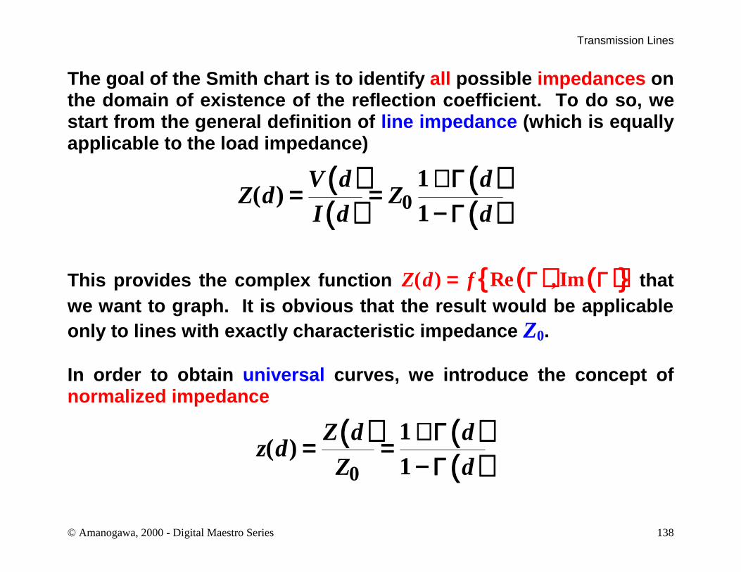
The goal of the Smith chart is to identify all possible impedances onthe domain of existence of the reflection coefficient. To do so, westart from the general definition of line impedance (which is equallyapplicable to the load impedance)
( )( )
( )( )0
1( )
1V d d
Z d ZI d d
+ Γ= =
− Γ
This provides the complex function ( ) ( ) ( ) Re , ImZ d f= Γ Γ thatwe want to graph. It is obvious that the result would be applicableonly to lines with exactly characteristic impedance Z0.
In order to obtain universal curves, we introduce the concept ofnormalized impedance
( ) ( )( )0
1( )
1Z d d
z dZ d
+ Γ= =
− Γ

Transmission Lines
© Amanogawa, 2000 - Digital Maestro Series 139
The normalized impedance is represented on the Smith chart byusing families of curves that identify the normalized resistance r(real part) and the normalized reactance x (imaginary part)
( ) ( ) ( )Re Imz d z j z r jx= + = +
Let’s represent the reflection coefficient in terms of its coordinates
( ) ( ) ( )Re Imd jΓ = Γ + Γ
Now we can write
( ) ( )( ) ( )( ) ( ) ( )
( )( ) ( )
2 2
2 2
1 Re Im1 Re Im
1 Re Im 2Im
1 Re Im
jr jx
j
j
+ Γ + Γ+ =
− Γ − Γ
− Γ − Γ + Γ=
− Γ + Γ

Transmission Lines
© Amanogawa, 2000 - Digital Maestro Series 140
The real part gives
( ) ( )( )( ) ( )
( )( ) ( )( ) ( ) ( )
( )( ) ( )( ) ( ) ( )
( ) ( ) ( )( )
( ) ( )
( ) ( ) ( )
2 2
2 2
2 2 2 2
2 2 2
22 2
2
2 22
1 Re Im
1 Re Im
1 1Re 1 Re 1 Im Im 0
1 1
1 1Re 1 Re 1 1 Im
1 1
11 Re 2 Re 1 Im
1 11
1Re Im
1 1
r
r rr r
r rr r
r rr r
r rr
r
r r
− Γ − Γ=
− Γ + Γ
Γ − + Γ − + Γ + Γ + − =+ +
Γ − + Γ − + + + Γ =+ +
+ Γ − Γ + + + Γ =+ ++
⇒ Γ − + Γ =+ +
= 0
Add a quantity equal to zero
Equation of a circle

Transmission Lines
© Amanogawa, 2000 - Digital Maestro Series 141
The imaginary part gives
( )( )( ) ( )
( )( ) ( ) ( )
( )( ) ( ) ( )
( )( ) ( ) ( )
( )( ) ( )
2 2
22 2
2 2
2 2
2 2
2 2
22
2
2 Im
1 Re Im
1 Re Im 2 Im 1 1 0
2 1 11 Re Im Im
2 1 11 Re Im Im
1 1Re 1 Im
x
x x
x x x
x x x
x x
Γ=
− Γ + Γ
− Γ + Γ − Γ + − =
− Γ + Γ − Γ + =
− Γ + Γ − Γ + =
⇒ Γ − + Γ − =
= 0
Multiply by x and add aquantit y equal to zero
Equation of a circle

Transmission Lines
© Amanogawa, 2000 - Digital Maestro Series 142
The result for the real part indicates that on the complex plane withcoordinates (Re( Γ), Im(Γ)) all the possible impedances with a givennormalized resistance r are found on a circle with
1, 0
1 1r
r r+ +Center = Radius =
As the normalized resistance r varies from 0 to ∞ , we obtain afamily of circles completely contained inside the domain of the
reflection coefficient | Γ | ≤ 1 .Im(Γ )
Re(Γ )
r = 0
r →∞
r = 1
r = 0.5
r = 5

Transmission Lines
© Amanogawa, 2000 - Digital Maestro Series 143
The result for the imaginary part indicates that on the complexplane with coordinates (Re( Γ), Im(Γ)) all the possible impedanceswith a given normalized reactance x are found on a circle with
1 11 ,
x xCenter = Radius =
As the normalized reactance x varies from -∞ to ∞ , we obtain afamily of arcs contained inside the domain of the reflection
coefficient | Γ | ≤ 1 .Im(Γ )
Re(Γ )
x = 0
x →±∞
x = 1
x = 0.5
x = -1x = - 0.5

Transmission Lines
© Amanogawa, 2000 - Digital Maestro Series 144
Basic Smith Chart techniques for loss-less transmission lines
Given Z(d) ⇒ Find Γ(d)Given Γ(d) ⇒ Find Z(d)
Given ΓR and ZR ⇒ Find Γ(d) and Z(d)Given Γ(d) and Z(d) ⇒ Find ΓR and ZR
Find dmax and dmin (maximum and minimum locations for thevoltage standing wave pattern)
Find the Voltage Standing Wave Ratio (VSWR)
Given Z(d) ⇒ Find Y(d)Given Y(d) ⇒ Find Z(d)

Transmission Lines
© Amanogawa, 2000 - Digital Maestro Series 145
Given Z(d) ⇒ Find Γ(d)
1. Normalize the impedance
( ) ( )0 0 0
dd
Z R Xz j r j x
Z Z Z= = + = +
2. Find the circle of constant normalized resistance r3. Find the arc of constant normalized reactance x4. The intersection of the two curves indicates the reflection
coefficient in the complex plane. The chart providesdirectly the magnitude and the phase angle of Γ(d)
Example : Find Γ(d), given
( ) 0d 25 100 with 50Z j Z= + Ω = Ω

Transmission Lines
© Amanogawa, 2000 - Digital Maestro Series 146
1
-1
0 0.2 0.5 5
0.2
-0.2
21
-0 5
0 5
-3
32
-2
1. Normalization
z (d) = (25 + j 100)/50
= 0.5 + j 2.0
2. Find normalized resistance circle
r = 0.5
3. Find normalized reactance arc
x = 2.0
4. This vector represents the reflection coefficient
Γ (d) = 0.52 + j0.64
|Γ (d)| = 0.8246
∠∠ Γ (d) = 0.8885 rad = 50.906 °
50.906 °
1.
0.8246

Transmission Lines
© Amanogawa, 2000 - Digital Maestro Series 147
Given Γ(d) ⇒ Find Z(d)
1. Determine the complex point representing the givenreflection coefficient Γ(d) on the chart.
2. Read the values of the normalized resistance r and of thenormalized reactance x that correspond to the reflectioncoefficient point.
3. The normalized impedance is
( )dz r j x= +
and the actual impedance is
( ) ( )0 0 0 0(d) dZ Z z Z r j x Z r j Z x= = + = +

Transmission Lines
© Amanogawa, 2000 - Digital Maestro Series 148
Given ΓR and ZR ⇐⇒ Find Γ(d) and Z(d)
NOTE: the magnitude of the reflection coefficient is constant alonga loss-less transmission line terminated by a specified load, since
( ) ( )d exp 2 dR RjΓ = Γ − β = Γ
Therefore, on the complex plane, a circle with center at the origin
and radius | ΓR | represents all possible reflection coefficientsfound along the transmission line. When the circle of constantmagnitude of the reflection coefficient is drawn on the Smith chart,one can determine the values of the line impedance at any location .
The graphical step-by-step procedure is:
1. Identify the load reflection coefficient ΓR and thenormalized load impedance ZR on the Smith chart.

Transmission Lines
© Amanogawa, 2000 - Digital Maestro Series 149
2. Draw the circle of constant reflection coefficientamplitude |Γ(d)| =|ΓR|.
3. Starting from the point representing the load, travel onthe circle in the clockwise direction, by an angle
22 d 2 d
πθ = β =λ
4. The new location on the chart corresponds to location don the transmission line. Here, the values of Γ(d) andZ(d) can be read from the chart as before.
Example : Given
025 100 50RZ j Z= + Ω = Ωwith
find
( ) ( ) 0.18Z d d dΓ = λand for

Transmission Lines
© Amanogawa, 2000 - Digital Maestro Series 150
θ
1
-1
0 0.2 0.5 5
0.2
-0.2
21
-0 5
0 5
-3
32
-2
ΓR
zR
∠ ΓR
θθ = 2 β d = 2 (2π/λ) 0.18 λ = 2.262 rad = 129.6°
z(d)
Γ (d)Γ(d) = 0.8246 ∠-78.7° = 0.161 – j 0.809 z(d) = 0.236 – j1.192
Z(d) = z(d) × Z0 = 11.79 – j59.6 Ω
Circle with constant | Γ |

Transmission Lines
© Amanogawa, 2000 - Digital Maestro Series 151
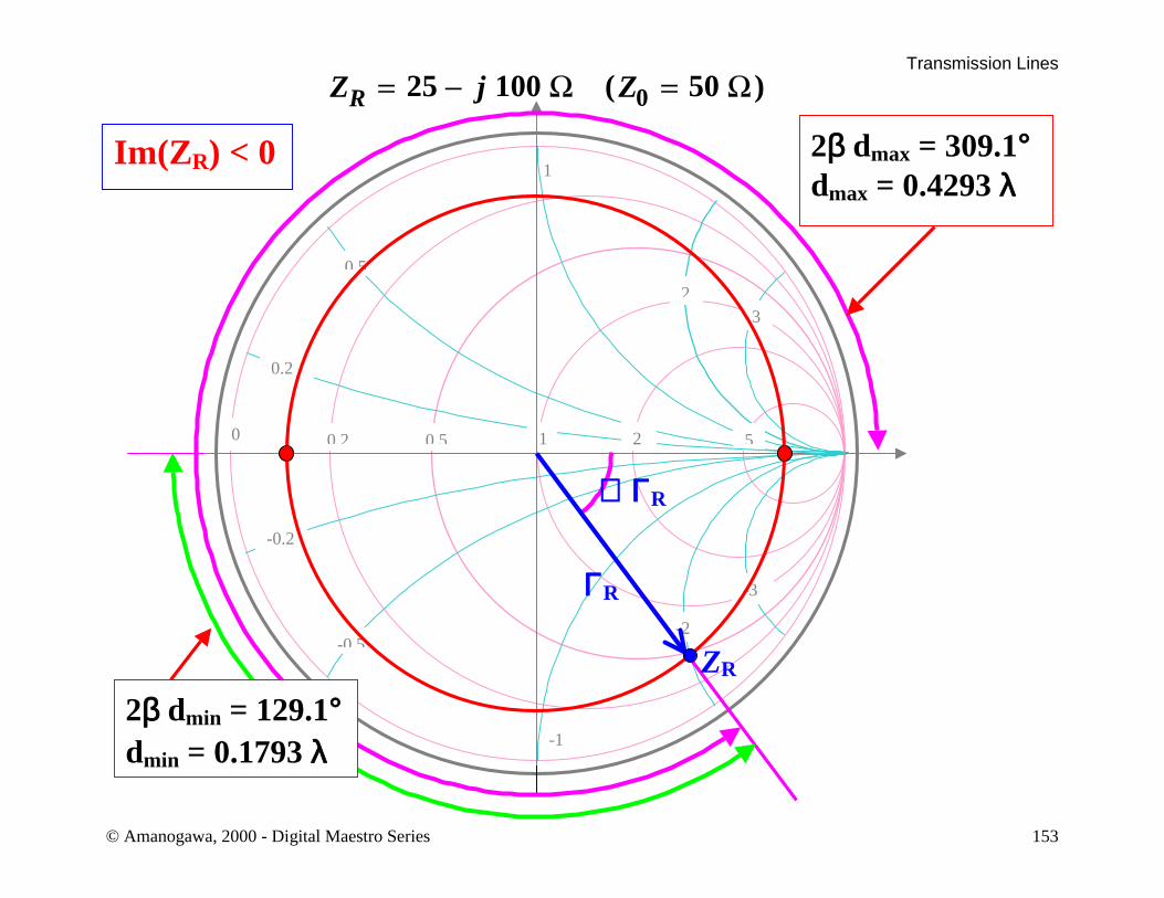
Given ΓR and ZR ⇒ Find dmax and dmin
1. Identify on the Smith chart the load reflection coefficientΓR or the normalized load impedance ZR .
2. Draw the circle of constant reflection coefficientamplitude |Γ(d)| =|ΓR|. The circle intersects the real axisof the reflection coefficient at two points which identifydmax (when Γ(d) = Real positive) and dmin (when Γ(d) =Real negative)
3. A commercial Smith chart provides an outer graduationwhere the distances normalized to the wavelength can beread directly. The angles, between the vector ΓR and thereal axis, also provide a way to compute dmax and dmin .
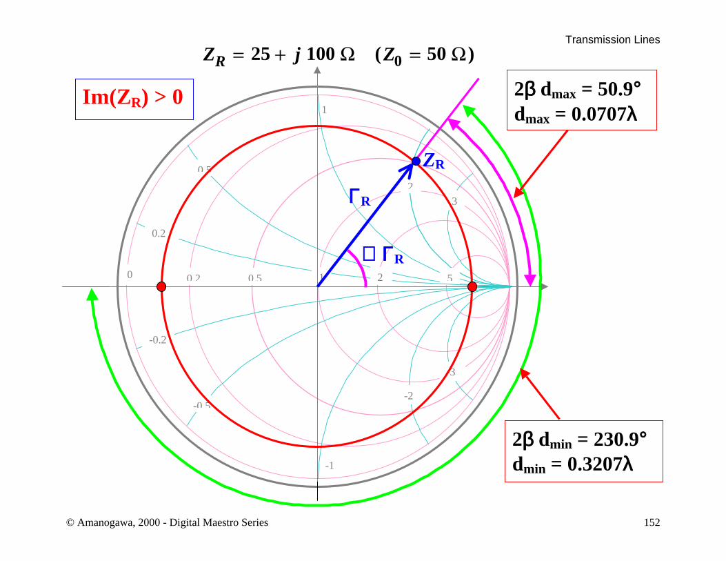
Example : Find dmax and dmin for
025 100 ; 25 100 ( 50 )R RZ j Z j Z= + Ω = − Ω = Ω
Transmission Lines
© Amanogawa, 2000 - Digital Maestro Series 152
1
-1
0 0.2 0.5 5
0.2
-0.2
21
-0 5
0 5
-3
32
-2
ΓR
ZR
∠ ΓR
2β dmin = 230.9°dmin = 0.3207λ
2β dmax = 50.9°dmax = 0.0707λ
Im(Z R) > 0
Z j ZR 25 100 500 ( )
Transmission Lines
© Amanogawa, 2000 - Digital Maestro Series 153
1
-1
0 0.2 0.5 5
0.2
-0.2
21
-0 5
0 5
-3
32
-2
ΓR
ZR
∠ ΓR
2β dmin = 129.1°dmin = 0.1793 λ
2β dmax = 309.1°dmax = 0.4293 λ
Im(Z R) < 0
Z j ZR 25 100 500 ( )

Transmission Lines
© Amanogawa, 2000 - Digital Maestro Series 154
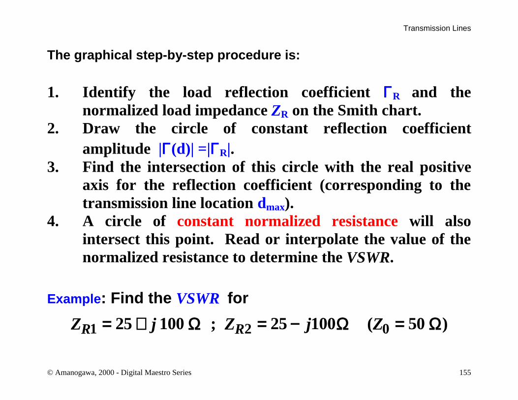
Given ΓR and ZR ⇒ Find the Voltage Standing Wave Ratio (VSWR)
The Voltage standing Wave Ratio or VSWR is defined as
max
min
11
R
R
VVSWR
V
+ Γ= =
− Γ
The normalized impedance at a maximum location of the standingwave pattern is given by
( ) ( )( )
maxmax
max
1 1!!!
1 1R
R
dz d VSWR
d
+ Γ + Γ= = =
− Γ − Γ
This quantity is always real and ≥ 1. The VSWR is simply obtainedon the Smith chart, by reading the value of the (real) normalizedimpedance, at the location dmax where Γ is real and positive .
Transmission Lines
© Amanogawa, 2000 - Digital Maestro Series 155
The graphical step-by-step procedure is:
1. Identify the load reflection coefficient ΓR and thenormalized load impedance ZR on the Smith chart.
2. Draw the circle of constant reflection coefficientamplitude |Γ(d)| =|ΓR|.
3. Find the intersection of this circle with the real positiveaxis for the reflection coefficient (corresponding to thetransmission line location dmax).
4. A circle of constant normalized resistance will alsointersect this point. Read or interpolate the value of thenormalized resistance to determine the VSWR.
Example : Find the VSWR for
1 2 025 100 ; 25 100 ( 50 )R RZ j Z j Z= + Ω = − Ω = Ω
Transmission Lines
© Amanogawa, 2000 - Digital Maestro Series 156
1
-1
0 0.2 0.5 5
0.2
-0.2
21
-0 5
0 5
-3
32
-2
ΓR1
zR1
zR2
ΓR2
Circle with constant | Γ |
z(dmax )=10.4
For both loadsVSWR = 10.4
Circle of constantconductance r = 10.4

Transmission Lines
© Amanogawa, 2000 - Digital Maestro Series 157
Given Z(d) ⇐⇒ Find Y(d)
Note: The normalized impedance and admittance are defined as
( )( )
( )( )
1 1( ) ( )
1 1d d
z d y dd d
+ Γ − Γ= =
− Γ + Γ
Since
( )
( )( ) ( )
4
114
4 114
d d
dd
z d y ddd
λ Γ + = −Γ λ + Γ + − Γλ ⇒ + = = = λ + Γ − Γ +

Transmission Lines
© Amanogawa, 2000 - Digital Maestro Series 158
Keep in mind that the equality
( )4
z d y dλ + =
is only valid for normalized impedance and admittance. The actualvalues are given by
0
00
4 4
( )( ) ( )
Z d Z z d
y dY d Y y d
Z
λ λ + = ⋅ +
= ⋅ =
where Y0=1 /Z0 is the characteristic admittance of the transmission

Transmission Lines
© Amanogawa, 2000 - Digital Maestro Series 159
line.The graphical step-by-step procedure is:
1. Identify the load reflection coefficient ΓR and thenormalized load impedance ZR on the Smith chart.
2. Draw the circle of constant reflection coefficientamplitude |Γ(d)| =|ΓR|.
3. The normalized admittance is located at a point on thecircle of constant |Γ| which is diametrically opposite to thenormalized impedance.
Example : Given
025 100 with 50RZ j Z= + Ω = Ω
find YR .

Transmission Lines
© Amanogawa, 2000 - Digital Maestro Series 160
1
-1
0 0.2 0.5 5
0.2
-0.2
21
-0 5
0 5
-3
32
-2
z(d) = 0.5 + j 2.0Z(d) = 25 + j100 [ Ω ]
y(d) = 0.11765 – j 0.4706Y(d) = 0.002353 – j 0.009412 [ S ]z(d+λ/4) = 0.11765 – j 0.4706Z(d+λ/4) = 5.8824 – j 23.5294 [ Ω ]
Circle with constant | Γ |
θ = 180° = 2β⋅λ/4

Transmission Lines
© Amanogawa, 2000 - Digital Maestro Series 161
The Smith chart can be used for line admittances, by shifting thespace reference to the admittance location . After that, one canmove on the chart just reading the numerical values asrepresenting admittances.
Let’s review the impedance -admittance terminology:
Impedance = Resistance + j Reactance
Z R jX= +
Admittance = Conductance + j Susceptance
Y G jB= +On the impedance chart, the correct reflection coefficient is alwaysrepresented by the vector corresponding to the normalizedimpedance . Charts specifically prepared for admittances aremodified to give the correct reflection coefficient in correspondenceof admittance.

Transmission Lines
© Amanogawa, 2000 - Digital Maestro Series 162
Smith Chart forAdmittances
00.20.55
-0.2
0.2
2 1
0 5
-0 5
3
-3
-2
2
-1
1
Positive(capacitive)
susceptance
Negative(inductive)
susceptanceΓ
y(d) = 0.11765 – j 0.4706
z(d) = 0.5 + 2.0

Transmission Lines
© Amanogawa, 2000 - Digital Maestro Series 163
Since related impedance and admittance are on opposite sides ofthe same Smith chart, the imaginary parts always have differentsign.
Therefore, a positive (inductive) reactance corresponds to anegative (inductive) susceptance , while a negative (capacitive)reactance corresponds to a positive (capacitive) susceptance .
Numerically, we have
( )( ) 2 2
2 2 2 2
1z r j x y g j b
r j x
r j x r jxy
r j x r j x r xr x
g br x r x
= + = + =+
− −= =+ − +
⇒ = = −+ +

Transmission Lines
©Amanogawa, 2000 – Digital Maestro Series 164
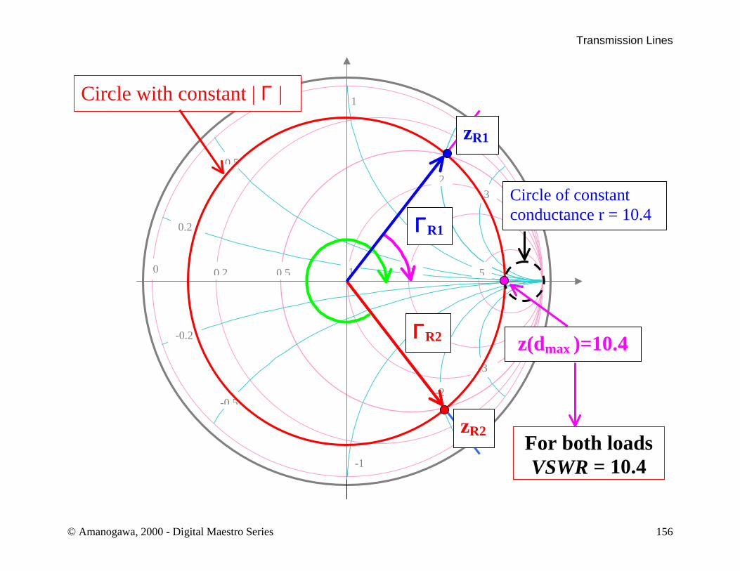
Impedance Matching A number of techniques can be used to eliminate reflections when line characteristic impedance and load impedance are mismatched. Impedance matching techniques can be designed to be effective for a specific frequency of operation ( narrow band techniques) or for a given frequency spectrum (broadband techniques ). One method of impedance matching involves the insertion of an impedance transformer between line and load
In the following, we neglect effects of loss in the lines.
Impedance Transformer Z0
ZR
Transmission Lines
©Amanogawa, 2000 – Digital Maestro Series 165
A simple narrow band impedance transformer consists of a transmission line section of length /4 The impedance transformer is positioned so that it is connected to a real impedance ZA. This is always possible if a location of maximum or minimum voltage standing wave pattern is selected.
ZA
dmax or dmin
ZR
/4
Z01 Z02 Z01
ZB

Transmission Lines
©Amanogawa, 2000 – Digital Maestro Series 166
Consider a general load impedance with its corresponding load reflection coefficient
01
01; expR
R R R R RR
Z ZZ R jX j
Z Z
If the transformer is inserted at a location of voltage maximum dmax
01 01
1 d 11 d 1
RA
RZ Z Z
If it is inserted instead at a location of voltage minimum dmin
01 01
1 d 11 d 1
RA
RZ Z Z

Transmission Lines
©Amanogawa, 2000 – Digital Maestro Series 167
Consider now the input impedance of a line of length /4 Since:
01 01
1 d 11 d 1
RA
RZ Z Z
we have
20 0
0tan L 0
tan( L)lim
tan( L)A
inA A
Z jZ ZZ Z
jZ Z Z
Z0
Zin ZA
L = /4

Transmission Lines
©Amanogawa, 2000 – Digital Maestro Series 168
Note that if the load is real , the voltage standing wave pattern at the load is maximum when ZR > Z01 or minimum when ZR < Z01 . The transformer can be connected directly at the load location or at a distance from the load corresponding to a multiple of /4 .
d1
ZA=Real
n /4 ; n=0,1,2…
ZR=Real
/4
Z01 Z02 Z01
ZB

Transmission Lines
©Amanogawa, 2000 – Digital Maestro Series 169
If the load impedance is real and the transformer is inserted at a distance from the load equal to an even multiple of /4 then
1; d 24 2A RZ Z n n
but if the distance from the load is an odd multiple of /4
201
1; d (2 1)4 2 4A
R
ZZ n n
Z

Transmission Lines
©Amanogawa, 2000 – Digital Maestro Series 170
The input impedance of the impedance transformer after inclusion in the circuit is given by
202
BA
ZZ
Z
For impedance matching we need
202
01 02 01 AA
ZZ Z Z Z
Z
The characteristic impedance of the transformer is simply the geometric average between the characteristic impedance of the original line and the load seen by the transformer. Let’s now review some simple examples.

Transmission Lines
©Amanogawa, 2000 – Digital Maestro Series 171
Real Load Impedance
202
01 02 01 50 100 70.71B RR
ZZ Z Z Z R
R
ZA
/4
RR = 100 Z01 = 50 Z02 = ?
ZB

Transmission Lines
©Amanogawa, 2000 – Digital Maestro Series 172
Note that an identical result is obtained by switching Z01 and RR
202
01 02 01 100 50 70.71B RR
ZZ Z Z Z R
R
ZA
/4
RR = 50 Z01 = 100 Z02 = ?
ZB

Transmission Lines
©Amanogawa, 2000 – Digital Maestro Series 173
Another real load case
202
01 02 01 75 300 150B RR
ZZ Z Z Z R
R
ZA
/4
RR = 300 Z01 = 75 Z02 = ?
ZB

Transmission Lines
©Amanogawa, 2000 – Digital Maestro Series 174
Same impedances as before, but now the transformer is inserted at a distance /4 from the load (voltage minimum in this case)
2 201 75
18.75300A
R
ZZ
R
202
01 02 01 75 18.75 37.5B AA
ZZ Z Z Z Z
Z
/4
ZA
RR = 300
/4
Z01 = 75 Z02 Z01
ZB

Transmission Lines
©Amanogawa, 2000 – Digital Maestro Series 175
Complex Load Impedance – Transformer at voltage maximum
0
100 100 500.62
100 100 50
1213.28
1
R
RA
R
jj
Z Z
02 01 50 213.28 103.27AZ Z Z
dmax
ZA
ZR = 100 + j 100
/4
Z01 = 50 Z02 Z01
ZB

Transmission Lines
©Amanogawa, 2000 – Digital Maestro Series 176
Complex Load Impedance – Transformer at voltage minimum
0
100 100 500.62
100 100 50
111.72
1
R
RA
R
jj
Z Z
02 01 50 11.72 24.21AZ Z Z
dmin
ZA
ZR = 100 + j 100
/4
Z01 = 50 Z02 Z01
ZB

Transmission Lines
©Amanogawa, 2000 – Digital Maestro Series 177
If it is not important to realize the impedance transformer with a quarter wavelength line, we can try to select a transmission line with appropriate length and characteristic impedance , such that the input impedance is the required real value
02
01 0202
tan( L)tan( L)
R RA
R R
R jX jZZ Z Z
Z j R jX
ZR = RR + jXR
L
Z01 Z02
ZA

Transmission Lines
©Amanogawa, 2000 – Digital Maestro Series 178
After separation of real and imaginary parts we obtain the equations
02 01 01
022
01 02
( ) tan L
tan L
R R
R
R
Z Z R Z X
Z X
Z R Z
with final solution
2 201
0201
2 201 01
1 /
1 /tan L
R R R
R
R R R R
R
Z R R XZ
R Z
R Z Z R R X
X
The transformer can be realized as long as the result for Z02 is real. Note that this is also a narrow band approach.

Transmission Lines
© Amanogawa, 2000 – Digital Maestro Series 179
Single stub impedance matching
Impedance matching can be achieved by inserting anothertransmission line ( stub ) as shown in the diagram below
ZA = Z0
dstub
ZRZ0
Lstub
Z0S

Transmission Lines
© Amanogawa, 2000 – Digital Maestro Series 180
There are two design parameters for single stub matching:
The location of the stub with reference to the load dstub
The length of the stub line Lstub
Any load impedance can be matched to the line by using singlestub technique. The drawback of this approach is that if the load ischanged, the location of insertion may have to be moved.
The transmission line realizing the stub is normally terminated by ashort or by an open circuit . In many cases it is also convenient toselect the same characteristic impedance used for the main line,although this is not necessary. The choice of open or shorted stubmay depend in practice on a number of factors. A short circuitedstub is less prone to leakage of electromagnetic radiation and issomewhat easier to realize. On the other hand, an open circuitedstub may be more practical for certain types of transmission lines,for example microstrips where one would have to drill the insulatingsubstrate to short circuit the two conductors of the line.

Transmission Lines
© Amanogawa, 2000 – Digital Maestro Series 181
Since the circuit is based on insertion of a parallel stub, it is moreconvenient to work with admittances , rather than impedances.
YA = Y0
dstub
YR = 1/ZRY0 = 1/Z0
Lstub
Y0S

Transmission Lines
© Amanogawa, 2000 – Digital Maestro Series 182
For proper impedance match:
( )stub stub 00
1dAY Y Y Y
Z= + = =
dstub
YR = 1/ZR
Y (dstub)
Lstub
Y0S
Ystub
+
Input admittanceof the stub line
Line admittance at locationdstub before the stub is applied

Transmission Lines
© Amanogawa, 2000 – Digital Maestro Series 183
In order to complete the design, we have to find an appropriatelocation for the stub. Note that the input admittance of a stub isalways imaginary (inductance if negative, or capacitance if positive)
stub stubY jB=A stub should be placed at a location where the line admittance hasreal part equal to Y0
( ) ( )stub 0 stubd dY Y jB= +
For matching, we need to have
( )stub stubdB B= −
Depending on the length of the transmission line, there may be anumber of possible locations where a stub can be inserted forimpedance matching. It is very convenient to analyze the possiblesolutions on a Smith chart.

Transmission Lines
© Amanogawa, 2000 – Digital Maestro Series 184
1
-1
0 0.2 0.5 5
0.2
-0.2
21
-0 5
0 5
-3
3
2
-2
zR
yR
Loadlocation
First locationsuitable forstub insertion
Second locationsuitable for stubinsertion
y(dstub1)
y(dstub2)
Unitaryconductancecircle
Constant|Γ(d)| circle
θ2
θ1

Transmission Lines
© Amanogawa, 2000 – Digital Maestro Series 185
The red arrow on the example indicates the load admittance . Thisprovides on the “admittance chart” the physical reference for theload location on the transmission line. Notice that in this case theload admittance falls outside the unitary conductance circle. If onemoves from load to generator on the line, the corresponding chartlocation moves from the reference point, in clockwise motion,according to an angle θθ (indicated by the light green arc)
42 d d
πθ = β =λ
The value of the admittance rides on the red circle whichcorresponds to constant magnitude of the line reflection coefficient,
|Γ(d)|=|ΓR |, imposed by the load.
Every circle of constant |Γ(d)| intersects the circle Re y = 1(unitary normalized conductance ), in correspondence of two points.Within the first revolution , the two intersections provide thelocations closest to the load for possible stub insertion.
Transmission Lines
© Amanogawa, 2000 – Digital Maestro Series 186
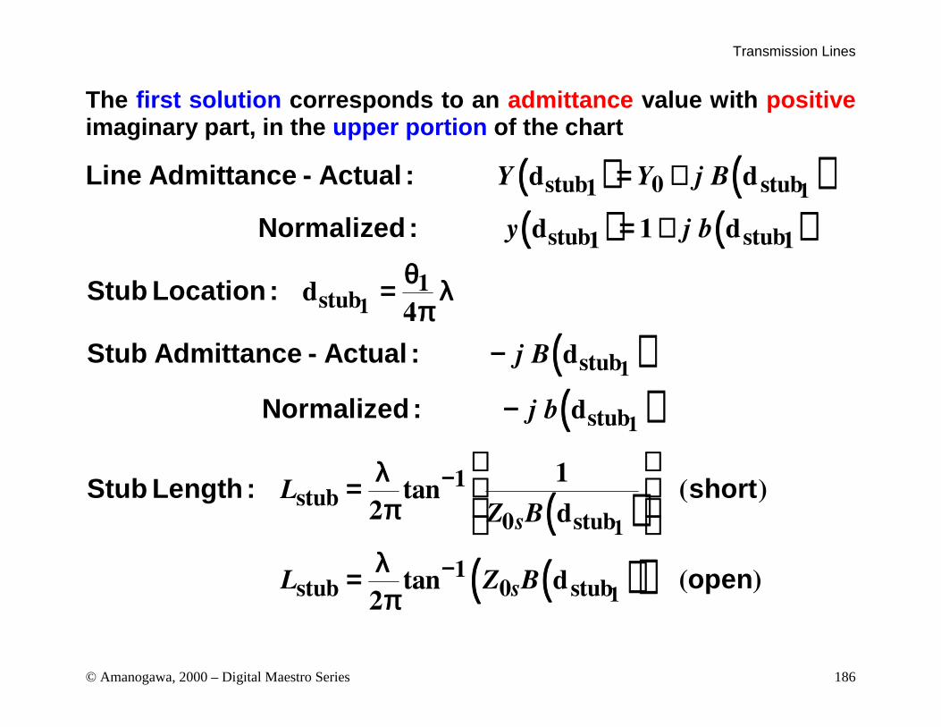
The first solution corresponds to an admittance value with positiveimaginary part, in the upper portion of the chart
( ) ( )( ) ( )
( )
1
1
1
stub 0 stub1
stub stub1 1
1stub
stub
d d
d 1 d
d4
d
Y Y j B
y j b
j B
= +
= +
θ= λπ
−
Line Admittance - Actual :
Normalized :
Stub Location :
Stub Admittance - Actual :
Norma ( )
( )( )( )
1
1
1
stub
1stub
0 stub
1stub 0 stub
d
1tan ( )
2 d
tan d ( )2
s
s
j b
LZ B
L Z B
−
−
−
λ = π
λ=π
lized :
Stub Length : short
open

Transmission Lines
© Amanogawa, 2000 – Digital Maestro Series 187
The second solution corresponds to an admittance value withnegative imaginary part, in the lower portion of the chart
( ) ( )( ) ( )
( )
2
2
2
stub 0 stub2
stub stub2 2
2stub
stub
d d
d 1 d
d4
d
Y Y j B
y j b
j B
= −
= −
θ= λπ
Line Admittance - Actual :
Normalized :
Stub Location :
Stub Admittance - Actual :
Norma ( )
( )( )( )
2
2
2
stub
1stub
0 stub
1stub 0 stub
d
1tan ( )
2 d
tan d ( )2
s
s
j b
LZ B
L Z B
−
−
λ = − π
λ= −π
lized :
Stub Length : short
open

Transmission Lines
© Amanogawa, 2000 – Digital Maestro Series 188
If the normalized load admittance falls inside the unitaryconductance circle (see next figure), the first possible stub locationcorresponds to a line admittance with negative imaginary part. Thesecond possible location has line admittance with positiveimaginary part. In this case, the formulae given above for first andsecond solution exchange place.
If one moves further away from the load, other suitable locations forstub insertion are found by moving toward the generator, atdistances multiple of half a wavelength from the original solutions.These locations correspond to the same points on the Smith chart.
1
2
stub
stub
d2
d2
n
n=
λ= +
λ+
First set of locations
Second set of locations

Transmission Lines
© Amanogawa, 2000 – Digital Maestro Series 189
1
-1
0 0.2 0.5 5
0.2
-0.2
21
-0 5
0 5
-3
3
2
-2
yR
zR
Loadlocation
Second locationsuitable for stubinsertion
First locationsuitable for stubinsertion
y(dstub2)
y(dstub1)
Unitaryconductancecircle
Constant|Γ(d)| circle
θ2
θθ1

Transmission Lines
© Amanogawa, 2000 – Digital Maestro Series 190
Single stub matching problems can be solved on the Smith chartgraphically, using a compass and a ruler. This is a step-by-stepsummary of the procedure:
(a) Find the normalized load impedance and determine thecorresponding location on the chart.
(b) Draw the circle of constant magnitude of the reflectioncoefficient | Γ| for the given load.
(c) Determine the normalized load admittance on the chart. This isobtained by rotating 180 ° on the constant | Γ| circle, from theload impedance point. From now on, all values read on the chartare normalized admittances.

Transmission Lines
© Amanogawa, 2000 – Digital Maestro Series 191
1
-1
0 0.2 0.5 5
0.2
-0.2
21
-0 5
0 5
-3
3
2
-2
zR
yR
(c) Find the normalized loadadmittance knowing that
yR = z(d=λ /4 )From now on the chartrepresents admittances.
(a) Obtain the normalized load
impedance zR=ZR /Z0 and findits location on the Smith chart
(b) Draw theconstant |Γ(d)|circle180° = λ /4

Transmission Lines
© Amanogawa, 2000 – Digital Maestro Series 192
(d) Move from load admittance toward generator by riding on theconstant | Γ| circle, until the intersections with the unitarynormalized conductance circle are found. These intersectionscorrespond to possible locations for stub insertion. CommercialSmith charts provide graduations to determine the angles ofrotation as well as the distances from the load in units ofwavelength.
(e) Read the line normalized admittance in correspondence of thestub insertion locations determined in (d). These values willalways be of the form
( )( )
stub
stub
d 1 top half of chart
d 1 bottom half of chart
y jb
y jb
= +
= −

Transmission Lines
© Amanogawa, 2000 – Digital Maestro Series 193
1
-1
0 0.2 0.5 5
0.2
-0.2
21
-0 5
0 5
-3
3
2
-2
zR
yR
Loadlocation
First location suitable forstub insertion
dstub1=(θ1/4π)λ
θ1
(d) Move from load towardgenerator and stop at alocation where the realpart of the normalized lineadmittance is 1.
Unitaryconductancecircle
(e) Read here thevalue of thenormalized lineadmittancey(dstub1) = 1+jb
First Solution

Transmission Lines
© Amanogawa, 2000 – Digital Maestro Series 194
1
-1
0 0.2 0.5 5
0.2
-0.2
21
-0 5
0 5
-3
3
2
-2
zR
yR
Loadlocation
Second location suitablefor stub insertion
dstub2=(θ2/4π)λ
(e) Read here thevalue of thenormalized lineadmittancey(dstub2) = 1 - jb
Unitaryconductancecircle
θ2
(d) Move from loadtoward generator andstop at a locationwhere the real part ofthe normalized lineadmittance is 1.
Second Solution

Transmission Lines
© Amanogawa, 2000 – Digital Maestro Series 195
(f) Select the input normalized admittance of the stubs, by takingthe opposite of the corresponding imaginary part of the lineadmittance
( )( )
stub stub
stub stub
line: d 1 stub:
line: d 1 stub:
y jb y jb
y jb y jb
= + → = −
= − → = +(g) Use the chart to determine the length of the stub. The
imaginary normalized admittance values are found on the circleof zero conductance on the chart . On a commercial Smith chartone can use a printed scale to read the stub length in terms ofwavelength. We assume here that the stub line hascharacteristic impedance Z0 as the main line. If the stub has
characteristic impedance Z0S ≠ Z0 the values on the Smith chartmust be renormalized as
0 0
0 0
' s
s
Y Zjb jb jb
Y Z± = ± = ±

Transmission Lines
© Amanogawa, 2000 – Digital Maestro Series 196
1
-1
0 0.2 0.5 5
0.2
-0.2
21
-0 5
-3
3
2
-2
y = ∞Short circuit
0 5
(f) Normalized inputadmittance of stub
ystub = 0 - jb
(g) Arc to determine the length of ashort circuited stub with normalizedinput admittance - jb

Transmission Lines
© Amanogawa, 2000 – Digital Maestro Series 197
1
-1
0 0.2 0.5 5
0.2
-0.2
21
-0 5
-3
3
2
-2
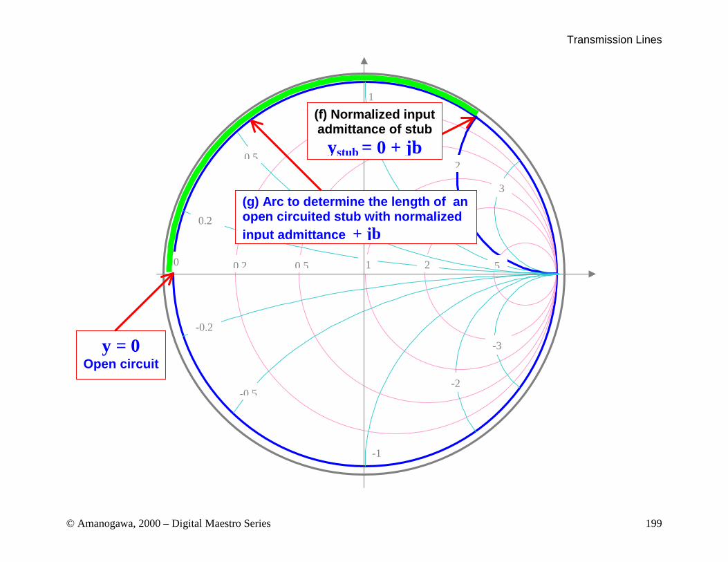
y = 0Open circuit
0 5
(f) Normalized inputadmittance of stub
ystub = 0 - jb
(g) Arc to determine the length of anopen circuited stub with normalizedinput admittance - jb

Transmission Lines
© Amanogawa, 2000 – Digital Maestro Series 198
1
-1
0 0.2 0.5 5
0.2
-0.2
21
-0 5
-3
3
2
-2
y = ∞Short circuit
0 5
(f) Normalized inputadmittance of stub
ystub = 0 + jb
(g) Arc to determine the length of ashort circuited stub with normalizedinput admittance + jb
Transmission Lines
© Amanogawa, 2000 – Digital Maestro Series 199
1
-1
0 0.2 0.5 5
0.2
-0.2
21
-0 5
-3
3
2
-2
0 5
(f) Normalized inputadmittance of stub
ystub = 0 + jb
(g) Arc to determine the length of anopen circuited stub with normalizedinput admittance + jb
y = 0Open circuit

Transmission Lines
© Amanogawa, 2000 – Digital Maestro Series 200
1
-1
0 0.2 0.5 5
0.2
-0.2
21
-0 5
0 5
-3
3
2
-2
yR
First Solution
After the stub is inserted,the admittance at the stublocation is moved to thecenter of the Smith chart,which corresponds tonormalized admittance 1and reflection coefficient 0(exact matching condition).
If you imagine to addgradually the negativeimaginary admittance ofthe inserted stub, the totaladmittance would followthe yellow arrow, reachingthe match point when thecomplete stub admittanceis added.
matchingcondition

Transmission Lines
© Amanogawa, 2000 – Digital Maestro Series 201
1
-1
0 0.2 0.5 5
0.2
-0.2
21
-0 5
0 5
-3
3
2
-2
yR
First Solution If the stub does not havethe proper normalized inputadmittance, the matchingcondition is not reached
Effect of a stub withpositive susceptance
Effect of a stub withnegative susceptance ofinsufficient magnitude
Effect of a stub withnegative susceptance ofexcessive magnitude

Transmission Lines
© Amanogawa, 2000 – Digital Maestro Series 202
Double stub impedance matching Impedance matching can be achieved by inserting two stubs at specified locations along transmission line as shown below
YA = Y01 dstub1
YR = 1/ZR Y01 = 1/Z01
Lstub1
Y0S1
Lstub2
Y0S2
dstub2
Transmission Lines
© Amanogawa, 2000 – Digital Maestro Series 203
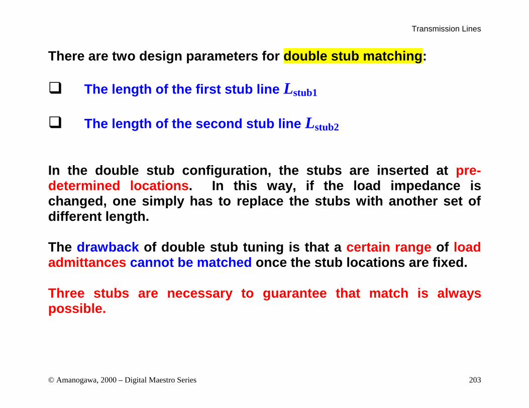
There are two design parameters for double stub matching: The length of the first stub line Lstub1
The length of the second stub line Lstub2 In the double stub configuration, the stubs are inserted at pre-determined locations . In this way, if the load impedance is changed, one simply has to replace the stubs with another set of different length. The drawback of double stub tuning is that a certain range of load admittances cannot be matched once the stub locations are fixed. Three stubs are necessary to guarantee that match is always possible.
Transmission Lines
© Amanogawa, 2000 – Digital Maestro Series 204
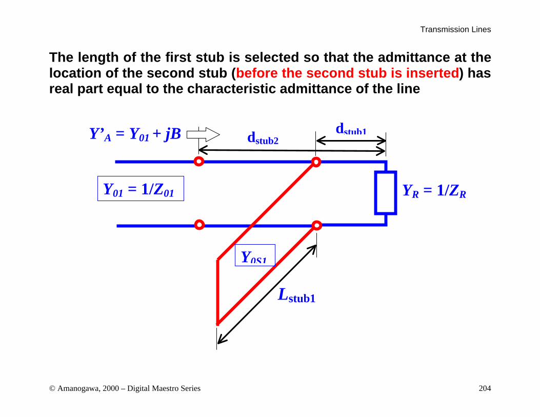
The length of the first stub is selected so that the admittance at the location of the second stub ( before the second stub is inserted ) has real part equal to the characteristic admittance of the line
Y’A = Y01 + jB dstub1
YR = 1/ZR Y01 = 1/Z01
Lstub1
Y0S1
dstub2

Transmission Lines
© Amanogawa, 2000 – Digital Maestro Series 205
The length of the second stub is selected to eliminate the imaginary part of the admittance at the location of insertion.
YA = Y01 + jB – jB = Y01 dstub1
YR = 1/ZR
Lstub1
Y0S1
dstub2
Lstub2
Y0S2
Y01 = 1/Z01
Ystub = -jB

Transmission Lines
© Amanogawa, 2000 – Digital Maestro Series 206
1
-1
0 0.2 0.5 5
0.2
-0.2
2 1
-0 5
0 5
-3
3
2
-2 The normalized admittance that we want at location
dstub2 is on this circle
At the location wherethe second stub isinserted, the possiblenormalized admittancesthat can give matchingare found on the circleof unitary conductanceon the Smith chart.

Transmission Lines
© Amanogawa, 2000 – Digital Maestro Series 207
YA = Y01
Lstub2
Y0S2
Y01 = 1/Z01
YR
dstub
Think of stub matching in a unified way.
Single stub
YR
Lstub1
Y0S1
Double stub
The two approaches solve the same problem
dstub2
Transmission Lines
© Amanogawa, 2000 – Digital Maestro Series 208
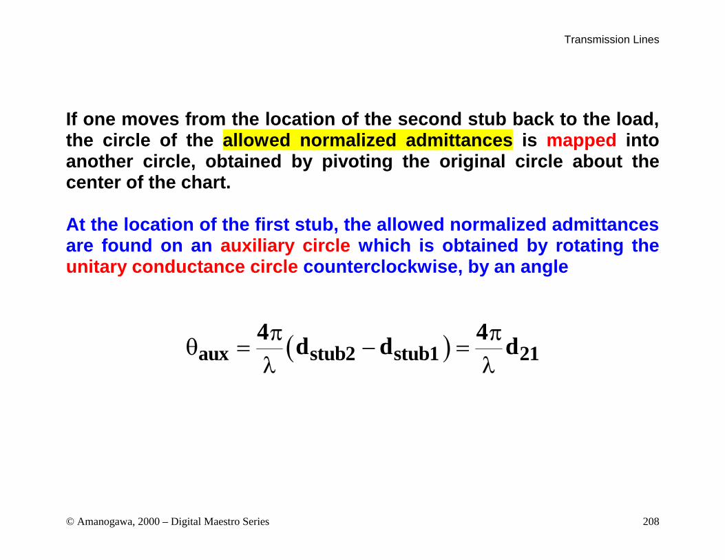
If one moves from the location of the second stub back to the load, the circle of the allowed normalized admittances is mapped into another circle, obtained by pivoting the original circle about the center of the chart. At the location of the first stub, the allowed normalized admittances are found on an auxiliary circle which is obtained by rotating the unitary conductance circle counterclockwise, by an angle
aux stub2 stub1 214 4
d d d

Transmission Lines
© Amanogawa, 2000 – Digital Maestro Series 209
1
-1
0 0.2 0.5 5
0.2
-0.2
2 1
0 5
-3
3
2
-2
aux
-0 5
The normalized admittance that we want at location dstub1 is on this auxiliary circle .
Pivot here
This angle of rotationcorresponds to a distance
d12 = dstub2 -dstub1

Transmission Lines
© Amanogawa, 2000 – Digital Maestro Series 210
1
-1
0 0.2 0.5 5
0.2
-0.2
2 1
0 5
-3
3
2
-2
aux
-0 5
This is the auxiliary circle fordistance between the stubsd21 = /8 + n /2.

Transmission Lines
© Amanogawa, 2000 – Digital Maestro Series 211
1
-1
0 0.2 0.5 5
0.2
-0.2
2 1
0 5
-3
3
2
-2
aux
-0 5
This is the auxiliary circle for distance between the stubs d21 = /4 + n /2.
Transmission Lines
© Amanogawa, 2000 – Digital Maestro Series 212
1
-1
0 0.2 0.5 5
0.2
-0.2
2 1
0 5
-3
3
2
-2
aux
-0 5
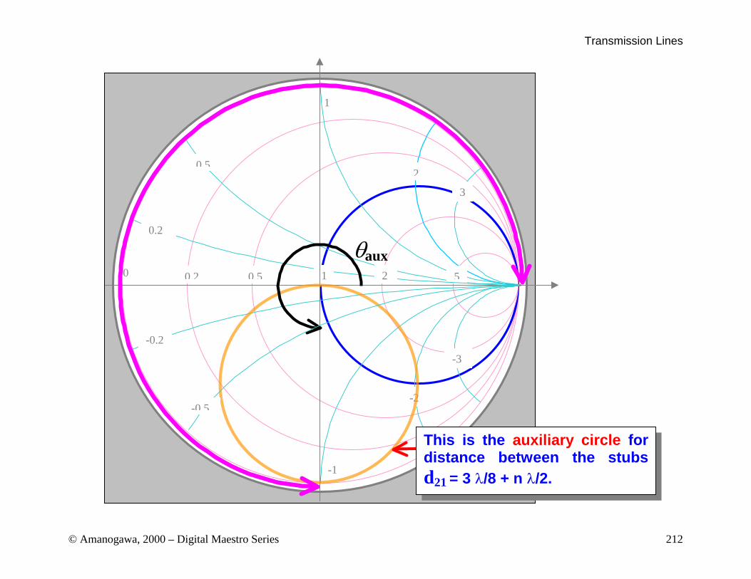
This is the auxiliary circle fordistance between the stubsd21 = 3 /8 + n /2.
Transmission Lines
© Amanogawa, 2000 – Digital Maestro Series 213
1
-1
0 0.2 0.5 5
0.2
-0.2
2 1
0 5
-3
3
2
-2
aux
-0 5
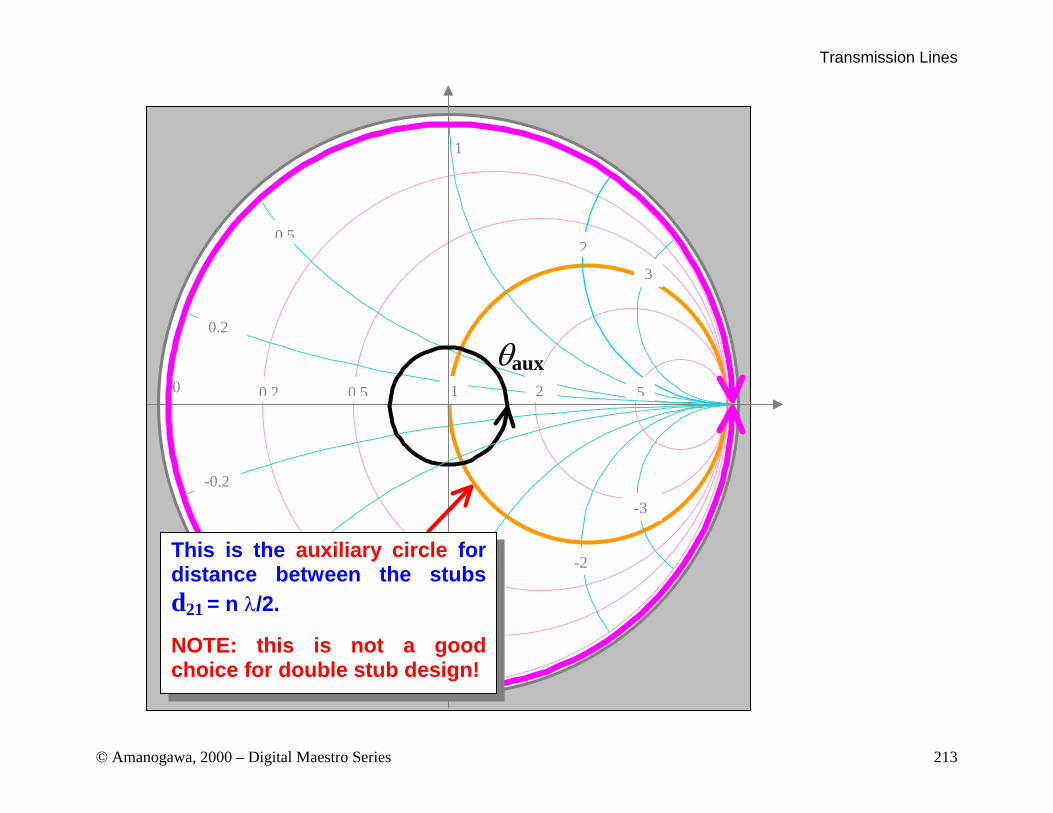
This is the auxiliary circle fordistance between the stubsd21 = n /2.
NOTE: this is not a goodchoice for double stub design!

Transmission Lines
© Amanogawa, 2000 – Digital Maestro Series 214
Given the load impedance, we need to follow these steps to complete the double stub design:
(a) Find the normalized load impedance and determine the corresponding location on the chart.
(b) Draw the circle of constant magnitude of the reflection coefficient | | for the given load.
(c) Determine the normalized load admittance on the chart. This is obtained by rotating -180 on the constant | | circle, from the load impedance point. From now on, all values read on the chart are normalized admittances.
(d) Find the normalized admittance at location dstub1 by moving clockwise on the constant | | circle.

Transmission Lines
© Amanogawa, 2000 – Digital Maestro Series 215
(e) Draw the auxiliary circle
(f) Add the first stub admittance so that the normalized admittance point on the Smith chart reaches the auxiliary circle (two possible solutions). The admittance point will move on the corresponding conductance circle, since the stub does not alter the real part of the admittance
(g) Map the normalized admittance obtained on the auxiliary circle to the location of the second stub dstub2. The point must be on the unitary conductance circle
(h) Add the second stub admittance so that the total parallel admittance equals the characteristic admittance of the line to achieve exact matching condition

Transmission Lines
© Amanogawa, 2000 – Digital Maestro Series 216
1
-1
0 0.2 0.5 5
0.2
-0.2
2 1
-0 5
0 5
-3
3
2
-2
zR
yR
(c) Find the normalized load admittance knowing that
yR = z(d= /4 ) From now on the chart represents admittances.
(a) Obtain the normalized load
impedance zR=ZR /Z0 and findits location on the Smith chart
(b) Draw the constant |(d)| circle 180 = /4
(d) Move to the first stub location

Transmission Lines
© Amanogawa, 2000 – Digital Maestro Series 217
1
-1
0 0.2 0.5 5
0.2
-0.2
2 1
-0 5
0 5
-3
3
2
-2
yR
(e) Draw the auxiliary circle
(f) Second solution: Add admittance of first stub to reach auxiliary circle
(f) First solution: Add admittance of first stub to reach auxiliary circle

Transmission Lines
© Amanogawa, 2000 – Digital Maestro Series 218
1
-1
0 0.2 0.5 5
0.2
-0.2
2 1
-0 5
0 5
-3
3
2
-2
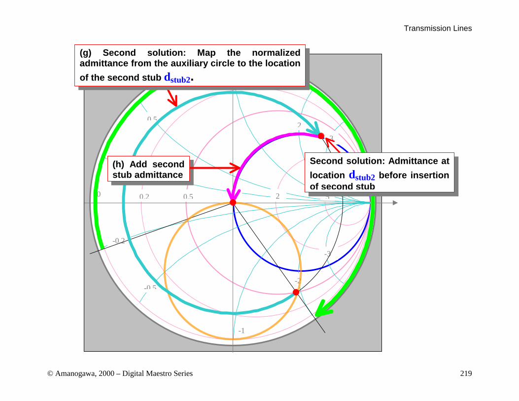
(g) First solution: Map the normalized admittance from the auxiliary circle to the location of the
second stub dstub2.
First solution: Admittance at
location dstub2 before insertionof second stub
(h) Add second stub admittance
Transmission Lines
© Amanogawa, 2000 – Digital Maestro Series 219
1
-1
0 0.2 0.5 5
0.2
-0.2
2 1
-0 5
0 5
-3
3
2
-2
(g) Second solution: Map the normalized admittance from the auxiliary circle to the location
of the second stub dstub2.
Second solution: Admittance at
location dstub2 before insertion of seco nd stub
(h) Add second stub admittance

Transmission Lines
© Amanogawa, 2000 – Digital Maestro Series 220
As mentioned earlier, a double stub configuration with fixed stub location may not be able to match a certain range of load impedances. This is easily seen on the Smith chart. If the normalized admittance of the line, at the first stub location , falls inside a certain forbidden conductance circle tangent to the auxiliary circle (and always contained inside the unitary conductance circle), it is not possible to find a value for the first stub that can bring the normalized admittance to the auxiliary circle. Therefore, it is impossible to position the normalized admittance of the second stub location on the unitary conductance circle. When this condition occurs, the location of one of the stubs must be changed appropriately. Alternatively, a third stub could be added. Examples of forbidden regions follow.

Transmission Lines
© Amanogawa, 2000 – Digital Maestro Series 221
1
-1
0 0.2 0.5 5
0.2
-0.2
2 1
0 5
-3
3
2
-2
aux
-0 5
This is the auxiliary circle fordistance between the stubsd21 = /8 + n /2.
The normalized conductance circlefor the normalized admittance doesnot intersect the auxiliary circle.
Forbidden conductance circle. If the admittance at the first stub location falls inside this circle, match is not possible with the given two stub confi guration.

Transmission Lines
© Amanogawa, 2000 – Digital Maestro Series 222
1
-1
0 0.2 0.5 5
0.2
-0.2
2 1
0 5
-3
3
2
-2
aux
-0 5
This is the auxiliary circle for distance between the stubs d21 = /4 + n /2.
Forbidden conductance
circle

Transmission Lines
© Amanogawa, 2000 – Digital Maestro Series 223
1
-1
0 0.2 0.5 5
0.2
-0.2
2 1
0 5
-3
3
2
-2
aux
-0 5
This is the auxiliary circle fordistance between the stubsd21 = 3 /8 + n /2.
Forbidden conductance
circle