SMD TFT-LCD MODEL NO. : LMS350DF01 - AllParts · Doc . No LMS350DF01 Rev.No 000 Page 4/30 Approval...
30
Doc . No LMS350DF01 Rev.No 000 Page 1/30 Approval TO : DATE : Sep.. 04. 2009 Customer Approval Any Modification of Spec is not allowed without SMD's permission. Approved by : Se chun, Oh Samsung Mobile Display Co. SMD TFT-LCD MODEL NO. : LMS350DF01
Transcript of SMD TFT-LCD MODEL NO. : LMS350DF01 - AllParts · Doc . No LMS350DF01 Rev.No 000 Page 4/30 Approval...
Doc . No LMS350DF01 Rev.No 000 Page 1/30
Approval
TO :DATE : Sep.. 04. 2009
Customer Approval
Any Modification of Spec is not allowed without SMD's permission.
Approved by : Se chun, Oh
Samsung Mobile Display Co.
SMD TFT-LCD
MODEL NO. : LMS350DF01

Doc . No LMS350DF01 Rev.No 000 Page 2/30
ApprovalContents
Revision History -------------------------- (3)General Description -------------------------- (4)1. Absolute Maximum Ratings -------------------------- (5)
1.1 Absolute Ratings Of Environment1.2 Electrical Absolute Ratings
2. Optical Characteristics -------------------------- (7)3. Electrical Characteristics ------------------------ (10)
3.1 TFT-LCD Module3.2 Back-light Unit
4. Block Diagram ------------------------- (11)4.1 TFT-LCD Module with Back Light Unit4.2 Back Light Unit
5. Input Terminal Pin Assignment ------------------------- (12)5.1 Input Signal & Power5.2 Input Signal, Basic Display Colors and Gray Scale of EachColors
6. Operation Specifications ------------------------ (14)6.1 Dot Formation6.2 Data Format for 8 bit RGB interface
7. Interface Timing ------------------------- (15)7.1 8bit RGB Interface Timing7.2 Serial Peripheral Interface
8. Electrical Specifications -------------------------- (17)9. Power Sequence ------------------------- (19)
9.1 Power on Sequence9.2 Power off Sequence9.3 Standby In / Out Sequence
10. Application Circuit --------------------------- (23)11. Module Outline Dimension --------------------------- (24)12. Reliability Test Result --------------------------- (25)
12.1 Condition12.2 Judgement
13. Packing --------------------------- (27)14. Marking and Others ------------------------- (29)15. General Precaution ------------------------- (30)
15.1 Handling15.2 Storage15.3 Operation15.4 Others

Doc . No LMS350DF01 Rev.No 000 Page 3/30
ApprovalData Rev.
No. Page Summary
Jan. 08. 2008
Jan. 30. 2008
.
June. 16. 2008
July. 09. 2008
July. 28. 2008
April. 09. 2009
August. 14. 2009
000
23
7
19
24
10
4
6
7
10
11
19
19
24
24
19
19
25
28
Rev.000 was first issued.
Power sequence added.
Interface changed. (RGB24bit→ RGB 8bit)
Logic Voltage changed. (VDD3 : 3.3V→ 1.8V)
Component description added.
Optical specification updated.
Power sequence revised.
Outline Dimension revised. (FPC length incresed 0.2mm.)
VDD3 = 3.3V added.
Typing error modified.
BLU Max current changed. (30mA→ 25mA)
Optecal specification updated..
Standby power consumption revised. & Dissipation check pattern changed.
Backlight power consumtion added.
Power On sequence revised.
Power On sequence revised.
Outline Dimension revised. (FPC silk revmoved.(top side))
Module thickness tolerance revised.
(Modify the Mechanical Information & Outline Dimension )
Power On Sequence revised.
Power On Sequence revised.
Reliability Test spec and result added.
Box label revised.
Revision History
Doc . No LMS350DF01 Rev.No 000 Page 4/30
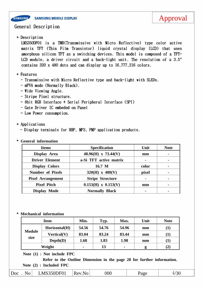
ApprovalGGGGeeeennnneeeerrrraaaallll DDDDeeeessssccccrrrriiiippppttttiiiioooonnnn
**** DDDDeeeessssccccrrrriiiippppttttiiiioooonnnn
LLLLMMMMSSSS333355550000DDDDFFFF00001111 iiiissss aaaa TTTTMMMMRRRR((((TTTTrrrraaaannnnssssmmmmiiiissssssssiiiivvvveeee wwwwiiiitttthhhh MMMMiiiiccccrrrroooo RRRReeeefffflllleeeeccccttttiiiivvvveeee)))) ttttyyyyppppeeee ccccoooolllloooorrrr aaaaccccttttiiiivvvveeee
mmmmaaaattttrrrriiiixxxx TTTTFFFFTTTT ((((TTTThhhhiiiinnnn FFFFiiiillllmmmm TTTTrrrraaaannnnssssiiiissssttttoooorrrr)))) lllliiiiqqqquuuuiiiidddd ccccrrrryyyyssssttttaaaallll ddddiiiissssppppllllaaaayyyy ((((LLLLCCCCDDDD)))) tttthhhhaaaatttt uuuusssseeeessss
aaaammmmoooorrrrpppphhhhoooouuuussss ssssiiiilllliiiiccccoooonnnn TTTTFFFFTTTT aaaassss aaaa sssswwwwiiiittttcccchhhhiiiinnnngggg ddddeeeevvvviiiicccceeeessss.... TTTThhhhiiiissss mmmmooooddddeeeellll iiiissss ccccoooommmmppppoooosssseeeedddd ooooffff aaaa TTTTFFFFTTTT----
LLLLCCCCDDDD mmmmoooodddduuuulllleeee,,,, aaaa ddddrrrriiiivvvveeeerrrr cccciiiirrrrccccuuuuiiiitttt aaaannnndddd aaaa bbbbaaaacccckkkk----lllliiiigggghhhhtttt uuuunnnniiiitttt.... TTTThhhheeee rrrreeeessssoooolllluuuuttttiiiioooonnnn ooooffff aaaa 3333....5555""""
ccccoooonnnnttttaaaaiiiinnnnssss 333322220000 xxxx 444488880000 ddddoooottttssss aaaannnndddd ccccaaaannnn ddddiiiissssppppllllaaaayyyy uuuupppp ttttoooo 11116666,,,,777777777777,,,,222211116666 ccccoooolllloooorrrrssss....
**** FFFFeeeeaaaattttuuuurrrreeeessss
---- TTTTrrrraaaannnnssssmmmmiiiissssssssiiiivvvveeee wwwwiiiitttthhhh MMMMiiiiccccrrrroooo RRRReeeefffflllleeeeccccttttiiiivvvveeee ttttyyyyppppeeee aaaannnndddd bbbbaaaacccckkkk----lllliiiigggghhhhtttt wwwwiiiitttthhhh 5555LLLLEEEEDDDDssss....
---- mmmmPPPPVVVVAAAA mmmmooooddddeeee ((((NNNNoooorrrrmmmmaaaallllllllyyyy BBBBllllaaaacccckkkk))))....
---- WWWWiiiiddddeeee VVVViiiieeeewwwwiiiinnnngggg AAAAnnnngggglllleeee....
---- SSSSttttrrrriiiippppeeee PPPPiiiixxxxeeeellll ssssttttrrrruuuuccccttttuuuurrrreeee....
---- 8888bbbbiiiitttt RRRRGGGGBBBB IIIInnnntttteeeerrrrffffaaaacccceeee ++++ SSSSeeeerrrriiiiaaaallll PPPPeeeerrrriiiipppphhhheeeerrrraaaallll IIIInnnntttteeeerrrrffffaaaacccceeee ((((SSSSPPPPIIII))))
---- GGGGaaaatttteeee DDDDrrrriiiivvvveeeerrrr IIIICCCC eeeemmmmbbbbeeeeddddeeeedddd oooonnnn PPPPaaaannnneeeellll
---- LLLLoooowwww PPPPoooowwwweeeerrrr ccccoooonnnnssssuuuummmmppppttttiiiioooonnnn....
**** AAAApppppppplllliiiiccccaaaattttiiiioooonnnnssss
---- DDDDiiiissssppppllllaaaayyyy tttteeeerrrrmmmmiiiinnnnaaaallllssss ffffoooorrrr HHHHHHHHPPPP,,,, MMMMPPPP3333,,,, PPPPMMMMPPPP aaaapppppppplllliiiiccccaaaattttiiiioooonnnn pppprrrroooodddduuuuccccttttssss....
* General information
Items Specification Unit Note
Display Area 48.96(H) x 73.44(V) mm -
Driver Element a-Si TFT active matrix - -
Display Colors 16.7 M color -
Number of Pixels 320(H) x 480(V) pixel -
Pixel Arrangement Stripe Structure - -
Pixel Pitch 0.153(H) x 0.153(V) mm -
Display Mode Normally Black - -
* Mechanical information
Item Min. Typ. Max. Unit Note
Module
size
Horizontal(H) 54.56 54.76 54.96 mm (1)
Vertical(V) 83.04 83.24 83.44 mm (1)
Depth(D) 1.68 1.83 1.98 mm (1)
Weight - 13 - g (2)
Note (1) : Not include FPCRefer to the Outline Dimension in the page 28 for further information.
Note (2) : Included FPC

Doc . No LMS350DF01 Rev.No 000 Page 5/30
Approval
1. Absolute Maximum Ratings
1.1 Absolute Ratings of Environment
Item Symbol Min. Max. Unit Note
Storage temperature TSTG -30 70 (1)
Operating temperature
(Ambient temperature)TOPR -20 60 (1),(2)
Note (1) 90 % RH Max. ( 50°C Ta )
Maximum wet-bulb temperature at 49°C or less. (Ta > 50°C)
No condensation.
(2) In case of below 0°, the response time of liquid crystal (L C) becomes
slower and the color of panel becomes darker than normal one. Level
of retardation depends on temperature, because of LC's char acteristics.
(3) If any fixed pattern is displayed on LCD for minutes, imag e-sticking
phenomenon may occur.
Doc . No LMS350DF01 Rev.No 000 Page 6/30
Approval
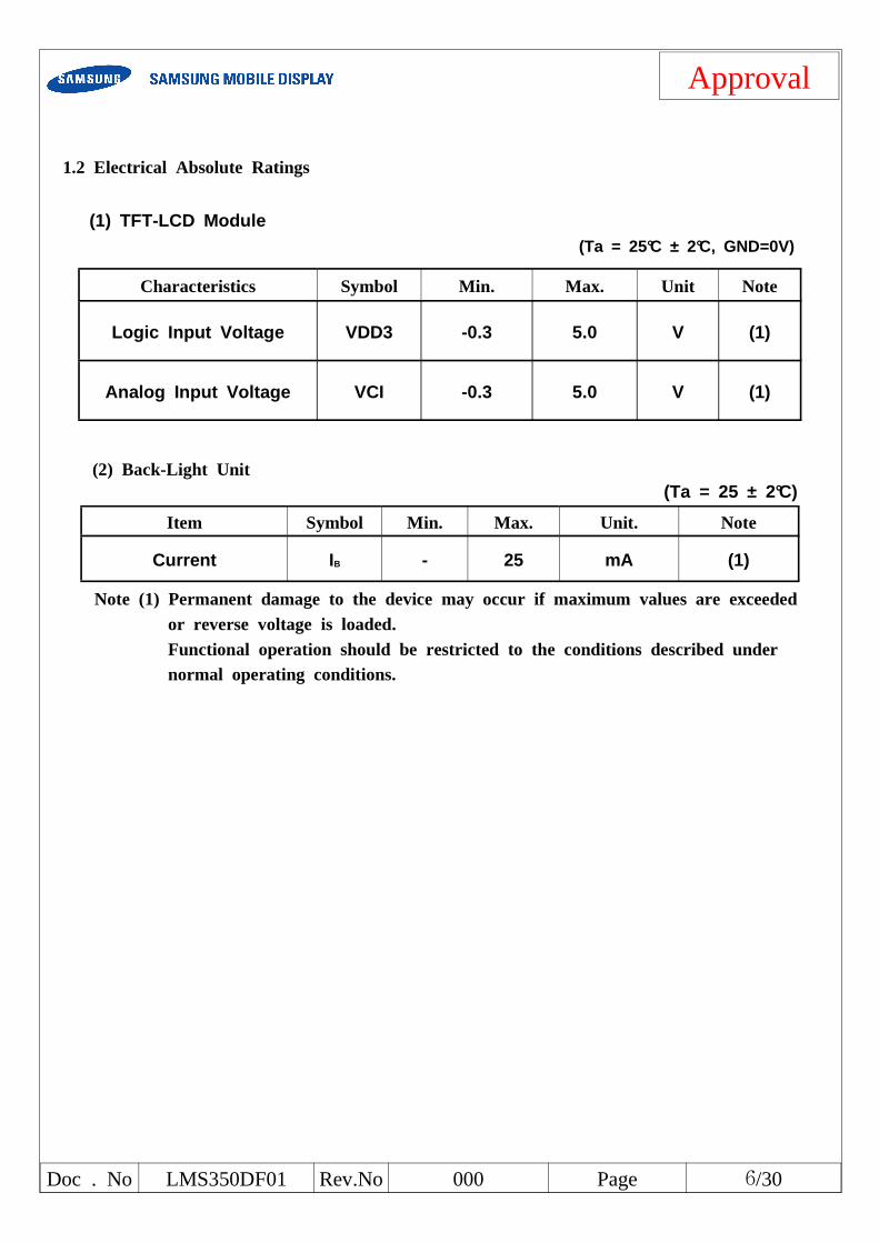
1.2 Electrical Absolute Ratings
(1) TFT-LCD Module(Ta = 25°C ± 2°C, GND=0V)
Characteristics Symbol Min. Max. Unit Note
Logic Input Voltage VDD3 -0.3 5.0 V (1)
Analog Input Voltage VCI -0.3 5.0 V (1)
(2) Back-Light Unit(Ta = 25 ± 2°C)
Item Symbol Min. Max. Unit. Note
Current I B - 25 mA (1)
Note (1) Permanent damage to the device may occur if maximum values are exceededor reverse voltage is loaded.Functional operation should be restricted to the conditions described undernormal operating conditions.

Doc . No LMS350DF01 Rev.No 000 Page 7/30
Approval2. Optical Characteristics
The following items are measured under stable conditions. T he optical
characteristics should be measured in a dark room or equival ent state with
the methods shown in Note (1). Measuring equipment: SR-3, BM -7, EZ-Contrast
(Ta ==== 25 ± 2°C, VDD3 = VCI = 3.3V, IB ==== 20mA)
Item Symbol Condition Min. Typ. Max. Unit Note
CCCCoooonnnnttttrrrraaaasssstttt rrrraaaattttiiiioooo
((((CCCCeeeennnntttteeeerrrr ppppooooiiiinnnntttt))))CCCC////RRRR
NNNNooootttteeee
((((1111)))),,,,((((6666))))
ΦΦΦΦ ==== 0000
θθθθ ==== 0000
NNNNoooorrrrmmmmaaaallll
VVVViiiieeeewwwwiiiinnnngggg
AAAAnnnngggglllleeee
BBBB////LLLL OOOOnnnn
555500000000 888800000000 ---- ----((((2222))))
SSSSRRRR----3333
LLLLuuuummmmiiiinnnnaaaannnncccceeee ooooffff wwwwhhhhiiiitttteeee
((((CCCCeeeennnntttteeeerrrr ppppooooiiiinnnntttt))))YYYYLLLL 222288885555 333388880000 ---- ccccdddd////mmmm2222
((((3333))))
SSSSRRRR----3333
RRRReeeessssppppoooonnnnsssseeee
ttttiiiimmmmeeee
RRRRiiiissssiiiinnnngggg::::TTTTrrrr
TTTTrrrr++++TTTTffff ---- 33330000 33335555 mmmmsssseeeecccc((((4444))))
BBBBMMMM----7777FFFFaaaalllllllliiiinnnngggg::::TTTTffff
CCCCoooolllloooorrrr
cccchhhhrrrroooommmmaaaattttiiiicccciiiittttyyyy
((((CCCCIIIIEEEE 1111999933331111))))
WWWWhhhhiiiitttteeeeWWWWxxxx 0000....222277770000 0000....333322220000 0000....333377770000
----((((5555))))
SSSSRRRR----3333
WWWWyyyy 0000....222299997777 0000....333344447777 0000....333399997777
RRRReeeeddddRRRRxxxx 0000....555555555555 0000....666600005555 0000....666655555555
RRRRyyyy 0000....222277778888 0000....333322228888 0000....333377778888
GGGGrrrreeeeeeeennnnGGGGxxxx 0000....222277778888 0000....333322228888 0000....333377778888
GGGGyyyy 0000....555533333333 0000....555588883333 0000....666633333333
BBBBlllluuuueeeeBBBBxxxx 0000....111100001111 0000....111155551111 0000....222200001111
BBBByyyy 0000....000066661111 0000....111111111111 0000....111166661111
VVVViiiieeeewwwwiiiinnnngggg
aaaannnngggglllleeee
HHHHoooorrrr....θθθθLLLL
CCCC////RRRR≥≥≥≥11110000
BBBB////LLLL OOOOnnnn
88880000 ---- ----
DDDDeeeeggggrrrreeeeeeeessss
((((6666))))
EEEEzzzz ----
CCCCoooonnnnttttrrrraaaasssstttt
θθθθRRRR 88880000 ---- ----
VVVVeeeerrrr....ΦΦΦΦHHHH 88880000 ---- ----
ΦΦΦΦLLLL 88880000 ---- ----

Doc . No LMS350DF01 Rev.No 000 Page 8/30
Approval
Note (1) Test Equipment Setup
After stabilizing and leaving the panel alone at a given temp erature for 30 min,the measurement should be executed. Measurement should be e xecutedin a stable, windless, and dark room. 30 min after lighting th e back-light.This should be measured in the center of screen.
- Environment condition : Ta = 25 ± 2 °C- Back-Light On condition
dddd==== 55550000CCCCmmmm
θθθθ====99990000°°°°±±±± 0000....3333°°°°
LLLLCCCCDDDD
LLLLMMMMDDDD
Note (2) Definition of Contrast Ratio (C/R) : Ratio of gray ma x (Gmax) &
gray min (Gmin) at the center point
C RG
G====
m a x
m in* Gmax : Luminance with all dots white
* Gmin : Luminance with all dots black
LMD : Ligh Mesurement Devices

Doc . No LMS350DF01 Rev.No 000 Page 9/30
Approval
Note (3) Definition of Luminance of White (YL)
: Luminance of white at the center point
Note (4) Definition of Response time : Sum of Tr and Tf (Field : 1°)
Note (5) Definition of Color Chromaticity (CIE 1931)
Color coordinate of white & red, green, blue at center point.
Note (6) Definition of Viewing Angle : Viewing angle range (C R≥≥≥≥10)
6 o’clockdirection
Normal Line
θ L
θ Rφ Hφ L 12 o’clock
direction
θR =90o
θ L =90o
φ = 0o,
x
x'y'
y
θ = 0o
φ H = 90o
φ L= 90o
Doc . No LMS350DF01 Rev.No 000 Page 10/30
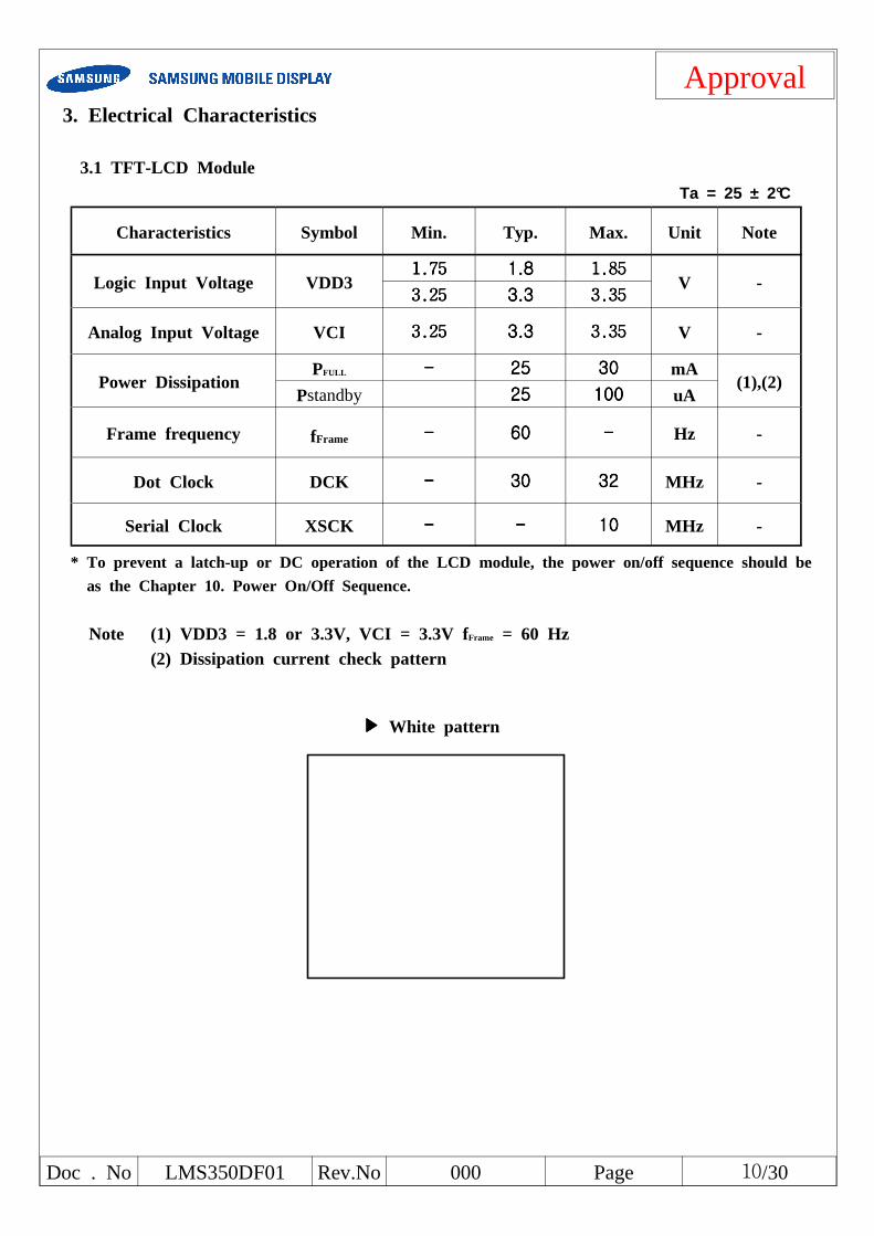
Approval3. Electrical Characteristics
3.1 TFT-LCD ModuleTa = 25 ± 2°C
Characteristics Symbol Min. Typ. Max. Unit Note
Logic Input Voltage VDD31111....77775555 1111....8888 1111....88885555
V -3333....22225555 3333....3333 3333....33335555
Analog Input Voltage VCI 3333....22225555 3333....3333 3333....33335555 V -
Power DissipationPFULL ---- 22225555 33330000 mA
(1),(2)Pstandby 22225555 111100000000 uA
Frame frequency fFrame ---- 66660000 ---- Hz -
Dot Clock DCK ---- 33330000 33332222 MHz -
Serial Clock XSCK ---- ---- 11110000 MHz -
* To prevent a latch-up or DC operation of the LCD module, the power on/off sequence should be
as the Chapter 10. Power On/Off Sequence.
Note (1) VDD3 = 1.8 or 3.3V, VCI = 3.3V fFrame = 60 Hz(2) Dissipation current check pattern
White pattern
Doc . No LMS350DF01 Rev.No 000 Page 11/30
Approval
3.2 Back-Light unit
The back-light system is an edge-lighting type with five white LED (Light EmittingDiode)s.
(Ta====25 ± 2°C)
Item Symbol Min. Typ. Max. Unit Note
Current I B - 20 - mA (1)
Power Consumption PBL - 330 - mW -
Note (1) Five LEDs serial type.
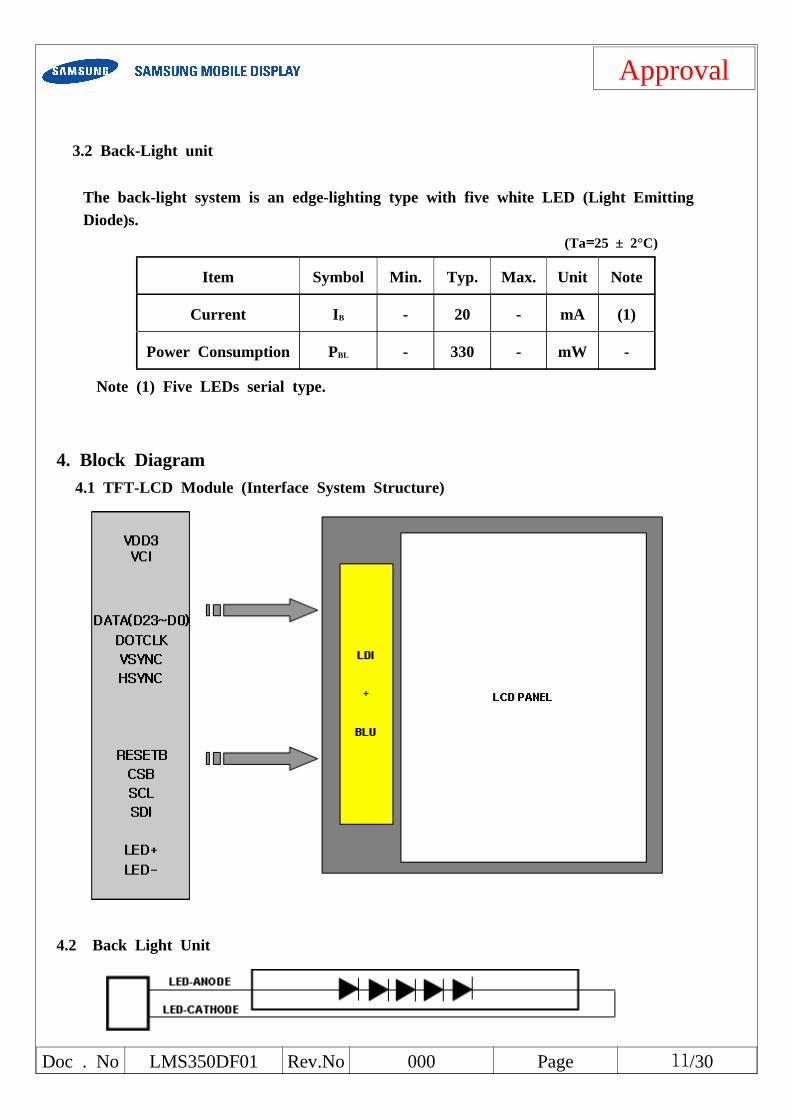
4. Block Diagram4.1 TFT-LCD Module (Interface System Structure)
4.2 Back Light Unit

Doc . No LMS350DF01 Rev.No 000 Page 12/30
Approval5. Input Terminal Pin Assignment
5.1 Input Signal & Power (8bit RGB I/F, BTB Connector: DF30FC-70DS-0.4V)
PinNo
Symbol Description I/OPin
NoSymbol Description I/O
1 LED+ LED Anode I 36 VCI Analog Input Voltage I
2 GND Ground I 37 PD10 GND or VDD3 I
3 NC No Connectior - 38 VCI Analog Input Voltage I
4 VGOFFL Power Output for ASG driver O 39 PD9 GND or VDD3 I
5 LED- LED Cathode I 40 C23M Charge Pumping Capacitor O
6 GND Ground I 41 PD8 GND or VDD3 I
7 GND Ground I 42 C23P Charge Pumping Capacitor O
8 VGL Gate Off Voltage O 43 GND GND or VDD3 I
9 PD23 D7 I 44 VCL Power Supply for Generating VCOML O
10 GND Ground I 45 PD7 GND or VDD3 I
11 PD22 D6 I 46 VSSA Ground I
12 VGH Gate On Voltage O 47 PD6 GND or VDD3 I
13 PD21 D5 I 48 VCOMH VCOM High Level O
14 C22P Charge Pumping Capacitor O 49 PD5 GND or VDD3 I
15 PD20 D4 I 50 VCOML VCOM Low Level O
16 C22M Charge Pumping Capacitor O 51 PD4 GND or VDD3 I
17 PD19 D3 I 52 GVDD Gamma Voltage Generator O
18 C21P Charge Pumping Capacitor O 53 PD3 GND or VDD3 I
19 PD18 D2 I 54 RVDD Regulated VDD output O
20 C21M Charge Pumping Capacitor O 55 PD2 GND or VDD3 I
21 PD17 D1 I 56 VDD3 Logic Input Voltage I
22 AVDD Power Output for Source Driver O 57 PD1 GND or VDD3 I
23 PD16 D0 I 58 VDD3 Logic Input Voltage I
24 C11Pb Charge Pumping Capacitor O 59 PD0 GND or VDD3 I
25 GND Ground I 60 VSYNC Vsync I
26 C11Mb Charge Pumping Capacitor O 61 GND Ground I
27 PD15 GND or VDD3 I 62 HSYNC Hsync I
28 C11P Charge Pumping Capacitor O 63 DOTCLK Dotclk I
29 PD14 GND or VDD3 I 64 SCL Serial Clock I
30 C11M Charge Pumping Capacitor O 65 SDI Serial Data Input I
31 PD13 GND or VDD3 I 66 CSB Chip Select I
32 VSSC Ground I 67 ENABLE Enable(GND) I
33 PD12 GND or VDD3 I 68 RESETB Reset I
34 VCI1 Reference Voltage In Step Up Circuit O 69 GND Ground I
35 PD11 GND or VDD3 I 70 GND Ground I

Doc . No LMS350DF01 Rev.No 000 Page 13/30
Approval5.2 Input Signal, Basic Display Colors and Gray Scale of EachColors
COLOR DISPLAY
DATA SIGNALGRAY
SCALE
LEVEL
RED GREEN BLUE
R0 R1 R2 R3 R4 R5 R6 R7 G0 G1 G2 G3 G4 G5 G6 G7 B0 B1 B2 B3 B4 B5 B6 B7
BASIC
COLOR
BLACK 0 0 0 0 0 0 0 0 0 0 0 0 0 0 0 0 0 0 0 0 0 0 0 0 -
BLUE 0 0 0 0 0 0 0 0 0 0 0 0 0 0 0 0 1 1 1 1 1 1 1 1 -
GREEN 0 0 0 0 0 0 0 0 1 1 1 1 1 1 1 1 0 0 0 0 0 0 0 0 -
CYAN 0 0 0 0 0 0 0 0 1 1 1 1 1 1 1 1 1 1 1 1 1 1 1 1 -
RED 1 1 1 1 1 1 1 1 0 0 0 0 0 0 0 0 0 0 0 0 0 0 0 0 -
MAGENTA 1 1 1 1 1 1 1 1 0 0 0 0 0 0 0 0 1 1 1 1 1 1 1 1 -
YELLOW 1 1 1 1 1 1 1 1 1 1 1 1 1 1 1 1 0 0 0 0 0 0 0 0 -
WHITE 1 1 1 1 1 1 1 1 1 1 1 1 1 1 1 1 1 1 1 1 1 1 1 1 -
GRAY
SCALE
OF
RED
BLACK 0 0 0 0 0 0 0 0 0 0 0 0 0 0 0 0 0 0 0 0 0 0 0 0 R0
DARK
↑
↓
LIGHT
1 0 0 0 0 0 0 0 0 0 0 0 0 0 0 0 0 0 0 0 0 0 0 0 R1
0 1 0 0 0 0 0 0 0 0 0 0 0 0 0 0 0 0 0 0 0 0 0 0 R2
: : : : : : : : : : : : : : : : : : : : : : : :R3~R252
: : : : : : : : : : : : : : : : : : : : : : : :
1 0 1 1 1 1 1 1 0 0 0 0 0 0 0 0 0 0 0 0 0 0 0 0 R253
0 1 1 1 1 1 1 1 0 0 0 0 0 0 0 0 0 0 0 0 0 0 0 0 R254
RED 1 1 1 1 1 1 1 1 0 0 0 0 0 0 0 0 0 0 0 0 0 0 0 0 R255
GRAY
SCALE
OF
GREEN
BLACK 0 0 0 0 0 0 0 0 0 0 0 0 0 0 0 0 0 0 0 0 0 0 0 0 G0
DARK
↑
↓
LIGHT
0 0 0 0 0 0 0 0 1 0 0 0 0 0 0 0 0 0 0 0 0 0 0 0 G1
0 0 0 0 0 0 0 0 0 1 0 0 0 0 0 0 0 0 0 0 0 0 0 0 G2
: : : : : : : : : : : : : : : : : :G3~G252
: : : : : : : : : : : : : : : : : :
0 0 0 0 0 0 0 0 1 0 1 1 1 1 1 1 0 0 0 0 0 0 0 0 G253
0 0 0 0 0 0 0 0 0 1 1 1 1 1 1 1 0 0 0 0 0 0 0 0 G254
GREEN 0 0 0 0 0 0 0 0 1 1 1 1 1 1 1 1 0 0 0 0 0 0 0 0 G255
GRAY
SCALE
OF
BLUE
BLACK 0 0 0 0 0 0 0 0 0 0 0 0 0 0 0 0 0 0 0 0 0 0 0 0 B0
DARK
↑
↓
LIGHT
0 0 0 0 0 0 0 0 0 0 0 0 0 0 0 0 1 0 0 0 0 0 0 0 B1
0 0 0 0 0 0 0 0 0 0 0 0 0 0 0 0 0 1 0 0 0 0 0 0 B2
: : : : : : : : : : : : : : : : : : : : : : : :B3~B252
: : : : : : : : : : : : : : : : : : : : : : : :
0 0 0 0 0 0 0 0 0 0 0 0 0 0 0 0 1 0 1 1 1 1 1 1 B253
0 0 0 0 0 0 0 0 0 0 0 0 0 0 0 0 0 1 1 1 1 1 1 1 B254
BLUE 0 0 0 0 0 0 0 0 0 0 0 0 0 0 0 0 1 1 1 1 1 1 1 1 B255
Note) Definition of Gray :
Rn : Red Gray, Gn : Green Gray, Bn : Blue Gray (n = Gray level)
Input Signal : 0 = Low level voltage, 1 = High level voltage
Doc . No LMS350DF01 Rev.No 000 Page 14/30
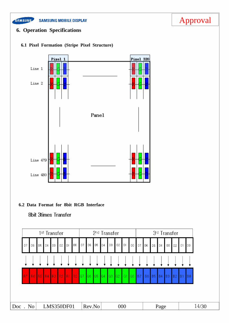
Approval6. Operation Specifications
6.1 Pixel Formation (Stripe Pixel Structure)
6.2 Data Format for 8bit RGB Interface

Doc . No LMS350DF01 Rev.No 000 Page 15/30
Approval7. Interface Timing
7.1 8bit RGB Interface Timing
* DOTCLK = [f frame × (480 + VBP + VFP) × (320 + HBP + HFP)]x3
= [(60)Hz × (480 + VBP + VFP) × (320 + HBP + HFP)]x3
* VBP ≥ 3 , VBP > VLW ≥ 2
* HBP ≥ 24 , HBP > HLW≥ 2
DATA[7:0]
HSYNC
HHHHLLLLWWWW====4444ccccllllkkkk
DOTCLK
HHHHBBBBPPPP[[[[8888::::0000]]]] >>>> HHHHLLLLWWWW ====11111111 ccccllllkkkk HHHHFFFFPPPP====5555ccccllllkkkk
Valid Data transfer area
1 Period(1Frame)
480H
HSYNC
VSYNCVVVVLLLLWWWW====2222HHHH
1 Horizontal Period
333322220000xxxx3333 ddddoooottttccccllllkkkk
VVVVBBBBPPPP[[[[7777::::0000]]]] >>>> VVVVLLLLWWWW ==== 6666HHHH
R G BR GB R G BR G B
1 320
VVVVFFFFPPPP====5555HHHH

Doc . No LMS350DF01 Rev.No 000 Page 16/30
Approval
7.2 Serial Peripheral Interface
(Note) RS="0": Index data
RS="1": Instruction data
1 2 3 4 5 76 8 9 10 11 12 13 14 15 16 17 18 19 20 21 22 23 24
RSDB15
DB14
DB13
DB12
DB11
DB10
DB9DB8DB7
DB4
DB6DB5
DB3DB2DB10000DB011111111111111110000
Transfer start Transfer end
LSBMSB
Device ID code RS R/W
Start byte Index register setting, instruction
////CCCCSSSS((((IIIInnnnppppuuuutttt))))
SSSSCCCCLLLL((((IIIInnnnppppuuuutttt))))
SSSSDDDDIIII((((IIIInnnnppppuuuutttt))))
0000

Doc . No LMS350DF01 Rev.No 000 Page 17/30
Approval8. Electrical Specifications
VDD3 = 1.8/3.3V, Ta = 25 ± 2
Item Symbol Min. Max. Unit
Serial Clock Cycle Time(write) tSCYCW 100 -
ns
Serial Clock rise/fall time tR,tF - 10
Pulse width high for write tSCHW 30 -
Pulse width low for write tSCLW 50
Chip Select Setup Time tCSS 20 -
Chip Select Hold Time tCSH 90 -
Serial Input Data Setup Time tSIDS 30 -
Serial Input Data Hold Time tSIDH 30 -
Serial Output Data delay Time tSODD - 200
Serial Output Data Hold Time tSODH 5 -
Reset Low Pulse Width tRES 30 -us
CSB Low Pulse Width for Wake up tCSBR 12 -

Doc . No LMS350DF01 Rev.No 000 Page 18/30
Approval
VDD3 = 1.8/3.3V, Ta = 25 ± 2 ((((8888bbbbiiiitttt))))
Item Symbol Min. Max. Unit
Vsync/Hsync Setup Time TvsysThsvs 20 -
ns
Vsync/Hsync Hold Time TvsyhThsyh 20 -
Dotclk Low Level Pulse Width tDCLW 17 -
Dotclk High Level Pulse Width tDCHW 17 -
Dotclk Cycle Time tDCYC 30 -
PD(Data) Setup Time tPDS 12 -
PD(Data) Hold Time tPDH 12 -
Dotclk Rise/Fall Time tR, tF - 5
PD[23:16]PD[23:16]
tF tR

Doc . No LMS350DF01 Rev.No 000 Page 19/30
Approval
Display ON
. Power On/Off Sequence (*Can be changed for better quality)9.1 Power On Sequence
R07h = 0101h
R07h = 0103h
/ RESET
R07h = 0000
Wait 1ms
Wait more than 10ms
Wait more than 6frames
Wait more than 2frame
Wait more than 5frames
POWER ON Sequence
Wait more than 1frame
R07h = 0001h
R11h = 222Fh
R12h = 0F00h
R13h = 7FE3h
R76h = 2213h
R74h = 0001h
R76h = 0000h
R10h = 5604h
R12h = 0C63h
DISPLAY ON Sequence
R01h = 0B3B (note1)
R02h = 0300
R03h = C040(note2)
R08h = 0004(note3)
R09h = 000B(note4)
R76h = 2213
R0Bh = 3340
R0Ch = 0020
R1Ch = 7770
R76h = 0000
R0Dh = 0000
R0Eh = 0500
R14h = 0000
R15h = 0803
R16h = 0000
R30h = 0005
R31h = 070F
R32h = 0300
R33h = 0003
R34h = 090C
R35h = 0001
R36h = 0001
R37h = 0303
R38h = 0F09
R39h = 0105
Doc . No LMS350DF01 Rev.No 000 Page 20/30
Approval
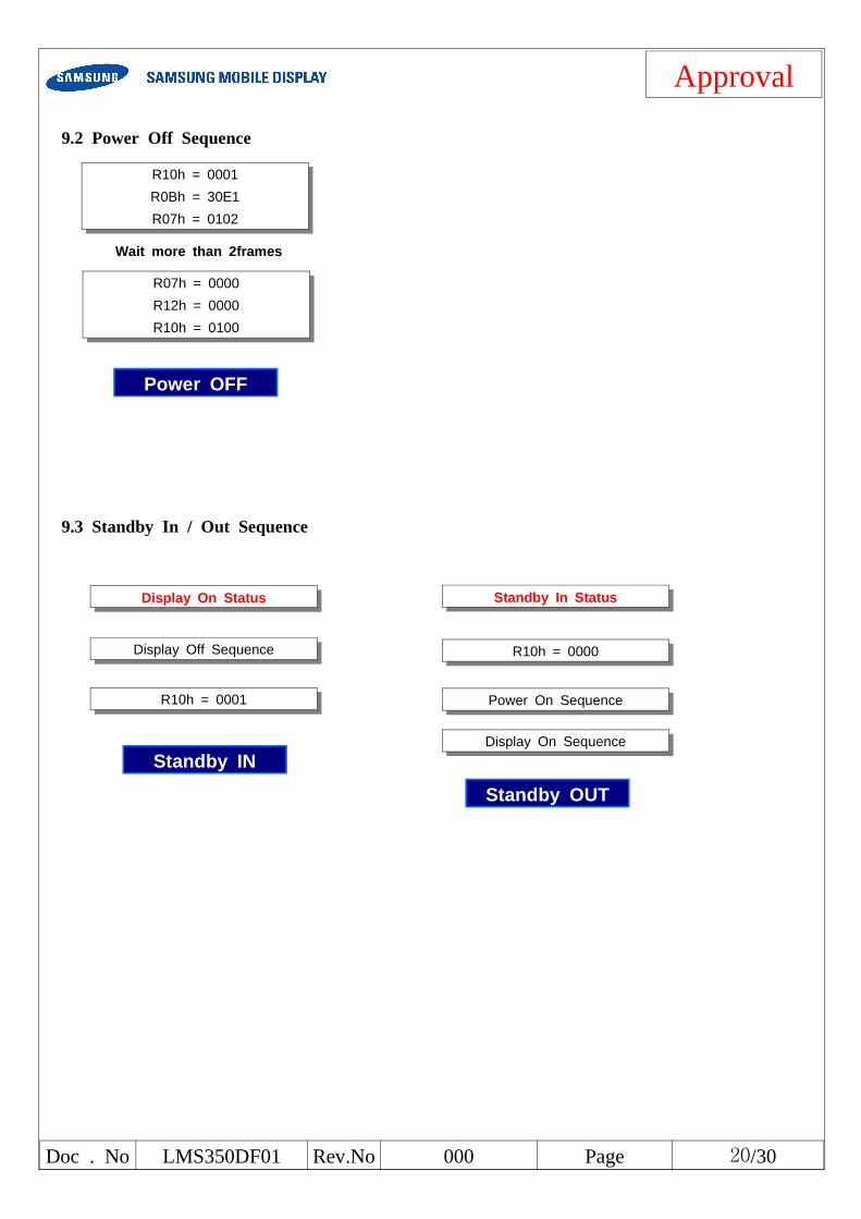
9.2 Power Off Sequence
9.3 Standby In / Out Sequence
R07h = 0000
R12h = 0000
R10h = 0100
R10h = 0001
R0Bh = 30E1
R07h = 0102
Wait more than 2frames
R10h = 0001
Display Off Sequence
Display On Status
Standby IN
R10h = 0000
Power On Sequence
Standby In Status
Standby OUT
Display On Sequence
Power OFF

Doc . No LMS350DF01 Rev.No 000 Page 21/30
ApprovalNote 1) Inversion Setting
* BGR : Color Inversion ( 0 : R ↔↔↔↔ B, 1 : bypass )
* TB : Vertical Inversion ( 0 : Bottom →→→→ Top, 1 : Top →→→→ Bottom )
* SS : Horizontal Inversion ( 0 : Right →→→→ Left, 1 : Left →→→→ Right )
Note 2) Polarity Setting
* VPL : Vsync Polarity (0 : High Active, 1 : Low Active)
* HPL : Hsync Polarity (0 : High Active, 1 : Low Active)
* DPL : Dotclk Polarity (0 : Data fetched at falling edge, 1 : at rising edge)
Note 3) VBP (Vsync Back Porch)
DB15 DB14 DB13 DB12 DB11 DB10 DB9 DB8 DB7 DB6 DB5 DB4 DB3 DB2 DB1DB0
0 0 0 0 0 0 0 0 VBP7 VBP6 VBP5 VBP4 VBP3 VBP2 VBP1 VBP0
* The porch period should meet the following condition.
257H ≥ VBP ≥ 3H , VBP > VLW
DB15 DB14 DB13 DB12 DB11 DB10 DB9 DB8 DB7 DB6 DB5 DB4 DB3 DB2 DB1DB0
VPL HPL DPL 0 0 0 0 0 0 1 0 0 0 0 0 0
DB15 DB14 DB13 DB12 DB11 DB10 DB9 DB8 DB7 DB6 DB5 DB4 DB3 DB2 DB1DB0
0 0 0 0 BGR 0 TB SS 0 0 1 1 1 0 1 1

Doc . No LMS350DF01 Rev.No 000 Page 22/30
ApprovalNote 4) HBP (Hsync Back Porch)
DB15 DB14 DB13 DB12 DB11 DB10 DB9 DB8 DB7 DB6 DB5 DB4 DB3 DB2 DB1DB0
0 0 0 0 0 0 0 HBP8 HBP7 HBP6 HBP5 HBP4 HBP3 HBP2 HBP1 HBP0
* The porch period should meet the following condition.
511dck≥ HBP ≥ 24dck , HBP > HLW
Approval
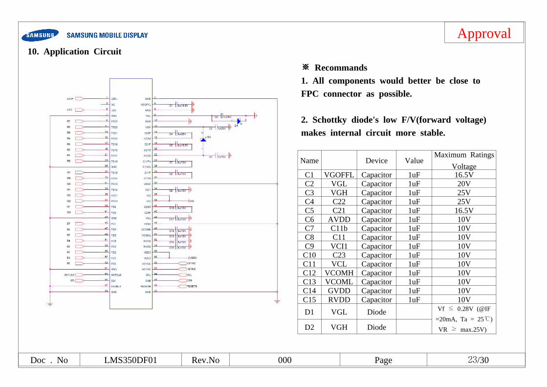
Doc . No LMS350DF01 Rev.No 000 Page 23/30
10. Application Circuit
※※※※ Recommands1. All components would better be close toFPC connector as possible.
2. Schottky diode's low F/V(forward voltage)makes internal circuit more stable.
Name Device ValueMaximum Ratings
VoltageC1 VGOFFL Capacitor 1uF 16.5VC2 VGL Capacitor 1uF 20VC3 VGH Capacitor 1uF 25VC4 C22 Capacitor 1uF 25VC5 C21 Capacitor 1uF 16.5VC6 AVDD Capacitor 1uF 10VC7 C11b Capacitor 1uF 10VC8 C11 Capacitor 1uF 10VC9 VCI1 Capacitor 1uF 10VC10 C23 Capacitor 1uF 10VC11 VCL Capacitor 1uF 10VC12 VCOMH Capacitor 1uF 10VC13 VCOML Capacitor 1uF 10VC14 GVDD Capacitor 1uF 10VC15 RVDD Capacitor 1uF 10V
D1 VGL Diode Vf ≤ 0.28V (@IF
=20mA, Ta = 25)
VR ≥ max.25V)D2 VGH Diode

Approval
Doc . No LMS350DF01 Rev.No 000 Page 24/30
11. Module outline Dimension
SAMSUNG MOBILEDISPLAY
Doc . No LMS350DF01 Rev.No 000 Page 25/30
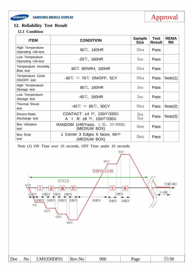
Approval12. Reliability Test Result
12.1 Condition
ITEM CONDITION SampleSize
TestResult
REMARK
High TemperatureOperating Life-test 60, 160HR 10ea Pass
Low TemperatureOperating Life-test -20, 160HR 5ea Pass
Temperature HumidityBias test 60 90%RH, 160HR 10ea Pass
Temperature CycleON/OFF test -30 ⇔ 70 ON/OFF, 5CY 10ea Pass Note(1)
High TemperatureStorage test 85, 160HR 5ea Pass
Low TemperatureStorage test -40, 160HR 5ea Pass
Thermal Shocktest -40 ⇔ 85, 30CY 10ea Pass Note(2)
Electro-StaticDischarge test
CONTACT: ±4 , 150/330ΩA I R: ±8 , 150/330Ω
5ea5ea Pass Note(3)
Box Vibrationtest
RANDOM 1HR/Yaxis, 1.5G, 10~200Hz(MEDIUM BOX) 1box Pass
Box Droptest
1 Corner 3 Edges 6 faces, 66(MEDIUM BOX)
1box Pass
Note (1) ON Time over 10 seconds, OFF Time under 10 seconds
70
-20
-30
30MIN30MIN 30MIN 30MIN 30MIN 90MIN
10MIN 10MIN 10MIN
60
30MIN
10MIN
-10
0
상온
25MIN
TEMPERATURE
1CYCLETIME(HR)
2~4HR
ⅠⅠⅠⅠ ⅡⅡⅡⅡ ⅢⅢⅢⅢ ⅣⅣⅣⅣ ⅤⅤⅤⅤ ⅣⅣⅣⅣ
Doc . No LMS350DF01 Rev.No 000 Page 26/30
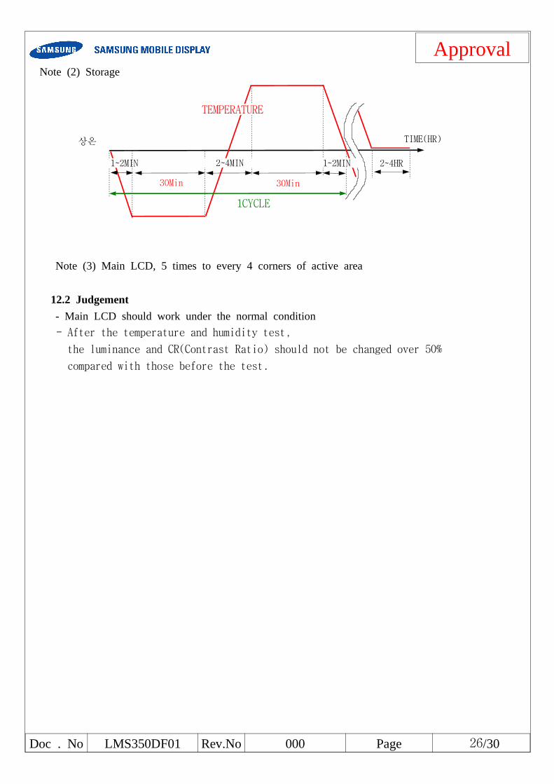
ApprovalNote (2) Storage
TEMPERATURE
30Min
상온
1~2MIN 2~4MIN
30Min
1~2MIN
1CYCLE
TIME(HR)
2~4HR
Note (3) Main LCD, 5 times to every 4 corners of active area
12.2 Judgement
- Main LCD should work under the normal condition
- After the temperature and humidity test,
the luminance and CR(Contrast Ratio) should not be changed over 50%
compared with those before the test.
Doc . No LMS350DF01 Rev.No 000 Page 27/30
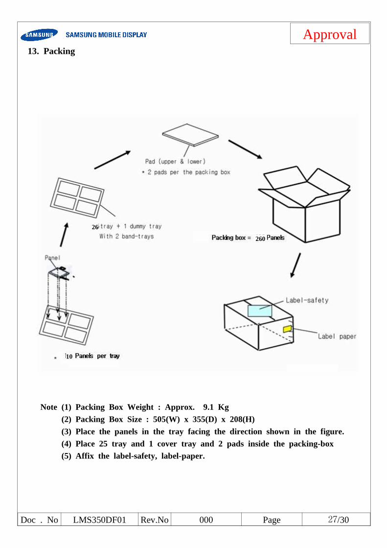
Approval13. Packing
Note (1) Packing Box Weight : Approx. 9.1 Kg
(2) Packing Box Size : 505(W) x 355(D) x 208(H)
(3) Place the panels in the tray facing the direction shown inthe figure.
(4) Place 25 tray and 1 cover tray and 2 pads inside the packing-box
(5) Affix the label-safety, label-paper.
26
10
260

Doc . No LMS350DF01 Rev.No 000 Page 28/30
Approval14. Marking & Others
(1) Packing case attach
260LMS350DF01
Doc . No LMS350DF01 Rev.No 000 Page 29/30
Approval15. General Precautions
15.1 Handling
(a) When the module is assembled, it should be attached to thesystem firmly. Becareful not to twist and bend the module.
(b) Refrain from strong mechanical shock and / or any force tothe module. Inaddition to damage, this may cause improper operation or damage to the moduleand back-light unit.
(c) Note that polarizers are very fragile and could be easilydamaged. Do not press orscratch the surface harder than a HB pencil lead.
(d) Wipe off water droplets or oil immediately. If you leave the droplets for a longtime, Staining and discoloration may occur.
(e) If the surface of the polarizer is dirty, clean it using some absorbent cotton orsoft cloth.
(f) The desirable cleaners are water, IPA(Isopropyl Alcohol) or Hexane. Do not useKetone type materials(ex. Acetone), Ethyl alcohol, Toluene, Ethyl acid or Methylchloride. It might permanent damage to the polarizer due to chemical reaction.
(g) If the liquid crystal material leaks from the panel, it should be kept away fromthe eyes or mouth. In case of contact with hands, legs or clothes, it must bewashed away thoroughly with soap.
(h) Protect the module from static, it may cause damage to theIntegrated GateCircuit.
(i) Use finger-stalls with soft gloves in order to keep display clean during the incominginspection and assembly process.
(j) Do not disassemble the module.
(k) Protection film for polarizer on the module shall be slowly peeled off just beforeuse so that the electrostatic charge can be minimized.
(l) Pins of I/F connector shall not be touched directly with bare hands

Doc . No LMS350DF01 Rev.No 000 Page 30/30
Approval15.2 Storage
(a) Do not leave the panel in high temperature, and high humidity for a long time. Itis highly recommended to store the module with temperature from 0 to 35°C andrelative humidity of less than 70%.
(b) Do not store the TFT-LCD module in direct sunlight.
(c) The module shall be stored in a dark place. It is prohibited to apply sunlight orfluorescent light during the store.
14.3 Operation
(a) Do not connect, disconnect the module in the "Power On" condition.
(b) Power supply should always be turned on/off by the "Poweron/off sequence"
14.4 Others
(a) The Liquid crystal is deteriorated by ultraviolet, do not leave it in direct sunlight
and strong ultraviolet ray for many hours.
(b) Avoid condensation of water. It may result in improper operation or disconnectionof electrode.
(c) Do not exceed the absolute maximum rating value. ( the supply voltage variation,input voltage variation, variation in part contents and environmental temperature,and so on) Otherwise the panel may be damaged.
(d) If the panel displays the same pattern continuously for along period of time, itcan be the situation when the image "Sticks" to the screen.
(e) This panel has its circuitry FPC on the bottom side and should be handledcarefully in order not to be stressed.