SLVSBD7A –JULY 2015 TPS65197x: 8-Channel Level … · The device converts the timing-controller...
12
CLKOUT1 CLKIN1 CLKIN2 CLKIN3 CLKIN4 CLKIN5 CLKIN6 Level Shifter CS_1 CLKOUT2 CS_2 CLKOUT3 CS_3 CLKOUT4 CS_4 CLKOUT5 CLKOUT6 STVOUT RESETOUT STVIN RESETIN DISCH1 DISCH2 Discharge DIS_SENSE VGH VGL1 VGL2 GND SEL_CS V(GH) V(GL1) V(GL2) V(CLK1) V(CLK2) V(CLK3) V(CLK4) V(CLK5) V(CLK6) V(STV) V(RESET) V(CLKOUT1) V(CLKOUT2) V(CLKOUT3) V(CLKOUT4) V(CLKOUT5) V(CLKOUT6) V(STVOUT) V(RESETOUT) TPS65197, TPS65197B SLVSBD7A – JULY 2015 TPS65197x: 8-Channel Level-Shifter Supporting No, 2-Channel and 3-Channel Charge-Sharing with Panel Discharge to VGH during Shut-Down 1 Features 3 Description The TPS65197/B is a 8-channel level-shifter with 1• 8-Channel Level-Shifter (STV, RESET, 6 × CLK) discharge function intended for use in LCD display • High Output-Voltage Level 16.5 V to 45 V (VGH) applications such as Notebooks, Monitors and TVs. • Low Output-Voltage Level Down to –20 V (VGL) The device converts the timing-controller (T-CON) • Selectable Charge-Sharing logic-level signals to the high-level signals needed by – No Charge-Sharing the gate-in-panel (GIP) display. – 2-Channel Charge-Sharing The clock outputs, CLKOUTx, support normal level – 3-Channel Charge-Sharing shifting operation and 2-channel or 3-channel charge- sharing, which can be used to improve picture quality • 2-Channel Panel Discharge and power consumption. At power down, all outputs • T-CON Failure Detection follow their input signals as long as possible; when – TPS65197: Logic Resets by STV Pulse the discharge function is used, the outputs are pulled high (V GH ). – TPS65197B: No Reset of the Logic • Latched Shut-Down Detection (Clocks to VGH) The TPS65197 implements a logic reset to ignore wrong T-CON signals after the rising STV edge which • Supports 100-kHz Clock Operating Frequency forces all 6 output clocks to VGL1. The next CLKIN1 • 28-Pin 4-mm × 4-mm QFN Package rising edge unlocks the logic and enables normal operation. The TPS65197B does not have the logic 2 Applications reset and follows always its input signals. • Gate-in-Panel (GIP) LCD Device Information (1) – Notebook PART NUMBER PACKAGE BODY SIZE (NOM) – Monitor TPS65197 WQFN (28) 4.00 mm x 4.00 mm – TV TPS65197B WQFN (28) 4.00 mm x 4.00 mm (1) For all available packages, see the orderable addendum at the end of the datasheet. 4 Simplified Schematic 1 An IMPORTANT NOTICE at the end of this data sheet addresses availability, warranty, changes, use in safety-critical applications, intellectual property matters and other important disclaimers. PRODUCTION DATA.
Transcript of SLVSBD7A –JULY 2015 TPS65197x: 8-Channel Level … · The device converts the timing-controller...

CLKOUT1
CLKIN1
CLKIN2
CLKIN3
CLKIN4
CLKIN5
CLKIN6
LevelShifter
CS_1
CLKOUT2
CS_2
CLKOUT3
CS_3
CLKOUT4
CS_4
CLKOUT5
CLKOUT6
STVOUT
RESETOUT
STVIN
RESETIN
DISCH1
DISCH2DischargeDIS_SENSE
VGH
VGL1
VGL2
GND
SEL_CS
V(GH)
V(GL1)
V(GL2)
V(CLK1)
V(CLK2)
V(CLK3)
V(CLK4)
V(CLK5)
V(CLK6)
V(STV)
V(RESET)
V(CLKOUT1)
V(CLKOUT2)
V(CLKOUT3)
V(CLKOUT4)
V(CLKOUT5)
V(CLKOUT6)
V(STVOUT)
V(RESETOUT)
TPS65197, TPS65197BSLVSBD7A –JULY 2015
TPS65197x: 8-Channel Level-Shifter Supporting No, 2-Channel and 3-ChannelCharge-Sharing with Panel Discharge to VGH during Shut-Down
1 Features 3 DescriptionThe TPS65197/B is a 8-channel level-shifter with
1• 8-Channel Level-Shifter (STV, RESET, 6 × CLK)discharge function intended for use in LCD display• High Output-Voltage Level 16.5 V to 45 V (VGH) applications such as Notebooks, Monitors and TVs.
• Low Output-Voltage Level Down to –20 V (VGL)The device converts the timing-controller (T-CON)
• Selectable Charge-Sharing logic-level signals to the high-level signals needed by– No Charge-Sharing the gate-in-panel (GIP) display.– 2-Channel Charge-Sharing The clock outputs, CLKOUTx, support normal level– 3-Channel Charge-Sharing shifting operation and 2-channel or 3-channel charge-
sharing, which can be used to improve picture quality• 2-Channel Panel Dischargeand power consumption. At power down, all outputs• T-CON Failure Detection follow their input signals as long as possible; when
– TPS65197: Logic Resets by STV Pulse the discharge function is used, the outputs are pulledhigh (VGH).– TPS65197B: No Reset of the Logic
• Latched Shut-Down Detection (Clocks to VGH) The TPS65197 implements a logic reset to ignorewrong T-CON signals after the rising STV edge which• Supports 100-kHz Clock Operating Frequencyforces all 6 output clocks to VGL1. The next CLKIN1• 28-Pin 4-mm × 4-mm QFN Package rising edge unlocks the logic and enables normaloperation. The TPS65197B does not have the logic2 Applications reset and follows always its input signals.
• Gate-in-Panel (GIP) LCDDevice Information(1)
– NotebookPART NUMBER PACKAGE BODY SIZE (NOM)
– MonitorTPS65197 WQFN (28) 4.00 mm x 4.00 mm
– TV TPS65197B WQFN (28) 4.00 mm x 4.00 mm
(1) For all available packages, see the orderable addendum atthe end of the datasheet.
4 Simplified Schematic
1
An IMPORTANT NOTICE at the end of this data sheet addresses availability, warranty, changes, use in safety-critical applications,intellectual property matters and other important disclaimers. PRODUCTION DATA.

TPS65197, TPS65197BSLVSBD7A –JULY 2015 www.ti.com
Table of Contents6.1 Documentation Support ........................................... 21 Features .................................................................. 16.2 Community Resources.............................................. 22 Applications ........................................................... 16.3 Trademarks ............................................................... 23 Description ............................................................. 16.4 Electrostatic Discharge Caution................................ 24 Simplified Schematic............................................. 16.5 Glossary .................................................................... 25 Revision History..................................................... 2
7 Mechanical, Packaging, and Orderable6 Device and Documentation Support.................... 2 Information ............................................................. 3
5 Revision History
Changes from Original (April 2012) to Revision A Page
• Added TPS65197B ................................................................................................................................................................ 1• Added Device and Documentation Support and Mechanical, Packaging, and Orderable Information sections ................... 2
6 Device and Documentation Support
6.1 Documentation Support
6.1.1 Related DocumentationPowerPAD™ Thermally Enhanced Package application report (SLMA002)PowerPAD™ Made Easy application report (SLMA004)QFN Layout Guidelines application report (SLOA122)QFN/SON PCB Attachment application report (SLUA271)
6.2 Community ResourcesThe following links connect to TI community resources. Linked contents are provided "AS IS" by the respectivecontributors. They do not constitute TI specifications and do not necessarily reflect TI's views; see TI's Terms ofUse.
TI E2E™ Online Community TI's Engineer-to-Engineer (E2E) Community. Created to foster collaborationamong engineers. At e2e.ti.com, you can ask questions, share knowledge, explore ideas and helpsolve problems with fellow engineers.
Design Support TI's Design Support Quickly find helpful E2E forums along with design support tools andcontact information for technical support.
6.3 TrademarksE2E is a trademark of Texas Instruments.All other trademarks are the property of their respective owners.
6.4 Electrostatic Discharge CautionThese devices have limited built-in ESD protection. The leads should be shorted together or the device placed in conductive foamduring storage or handling to prevent electrostatic damage to the MOS gates.
6.5 GlossarySLYZ022 — TI Glossary.
This glossary lists and explains terms, acronyms, and definitions.
2 Submit Documentation Feedback Copyright © 2015, Texas Instruments Incorporated
Product Folder Links: TPS65197 TPS65197B

TPS65197, TPS65197Bwww.ti.com SLVSBD7A –JULY 2015
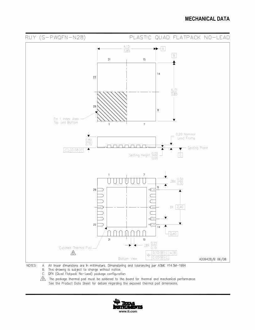
7 Mechanical, Packaging, and Orderable InformationThe following pages include mechanical, packaging, and orderable information. This information is the mostcurrent data available for the designated devices. This data is subject to change without notice and revision ofthis document. For browser-based versions of this data sheet, refer to the left-hand navigation.
Copyright © 2015, Texas Instruments Incorporated Submit Documentation Feedback 3
Product Folder Links: TPS65197 TPS65197B

To request a full data sheet, please send an email to: [email protected].

PACKAGE OPTION ADDENDUM
www.ti.com 4-Aug-2015
Addendum-Page 1
PACKAGING INFORMATION
Orderable Device Status(1)
Package Type PackageDrawing
Pins PackageQty
Eco Plan(2)
Lead/Ball Finish(6)
MSL Peak Temp(3)
Op Temp (°C) Device Marking(4/5)
Samples
TPS65197BRUYR ACTIVE WQFN RUY 28 3000 Green (RoHS& no Sb/Br)
CU NIPDAU Level-2-260C-1 YEAR -40 to 85 TPS65197B
TPS65197BRUYT ACTIVE WQFN RUY 28 250 Green (RoHS& no Sb/Br)
CU NIPDAU Level-2-260C-1 YEAR -40 to 85 TPS65197B
TPS65197RUYR ACTIVE WQFN RUY 28 3000 Green (RoHS& no Sb/Br)
CU NIPDAU Level-2-260C-1 YEAR -40 to 85 TPS65197A
TPS65197RUYT PREVIEW WQFN RUY 28 TBD Call TI Call TI -40 to 85 (1) The marketing status values are defined as follows:ACTIVE: Product device recommended for new designs.LIFEBUY: TI has announced that the device will be discontinued, and a lifetime-buy period is in effect.NRND: Not recommended for new designs. Device is in production to support existing customers, but TI does not recommend using this part in a new design.PREVIEW: Device has been announced but is not in production. Samples may or may not be available.OBSOLETE: TI has discontinued the production of the device.
(2) Eco Plan - The planned eco-friendly classification: Pb-Free (RoHS), Pb-Free (RoHS Exempt), or Green (RoHS & no Sb/Br) - please check http://www.ti.com/productcontent for the latest availabilityinformation and additional product content details.TBD: The Pb-Free/Green conversion plan has not been defined.Pb-Free (RoHS): TI's terms "Lead-Free" or "Pb-Free" mean semiconductor products that are compatible with the current RoHS requirements for all 6 substances, including the requirement thatlead not exceed 0.1% by weight in homogeneous materials. Where designed to be soldered at high temperatures, TI Pb-Free products are suitable for use in specified lead-free processes.Pb-Free (RoHS Exempt): This component has a RoHS exemption for either 1) lead-based flip-chip solder bumps used between the die and package, or 2) lead-based die adhesive used betweenthe die and leadframe. The component is otherwise considered Pb-Free (RoHS compatible) as defined above.Green (RoHS & no Sb/Br): TI defines "Green" to mean Pb-Free (RoHS compatible), and free of Bromine (Br) and Antimony (Sb) based flame retardants (Br or Sb do not exceed 0.1% by weightin homogeneous material)
(3) MSL, Peak Temp. - The Moisture Sensitivity Level rating according to the JEDEC industry standard classifications, and peak solder temperature.
(4) There may be additional marking, which relates to the logo, the lot trace code information, or the environmental category on the device.
(5) Multiple Device Markings will be inside parentheses. Only one Device Marking contained in parentheses and separated by a "~" will appear on a device. If a line is indented then it is a continuationof the previous line and the two combined represent the entire Device Marking for that device.
(6) Lead/Ball Finish - Orderable Devices may have multiple material finish options. Finish options are separated by a vertical ruled line. Lead/Ball Finish values may wrap to two lines if the finishvalue exceeds the maximum column width.

PACKAGE OPTION ADDENDUM
www.ti.com 4-Aug-2015
Addendum-Page 2
Important Information and Disclaimer:The information provided on this page represents TI's knowledge and belief as of the date that it is provided. TI bases its knowledge and belief on informationprovided by third parties, and makes no representation or warranty as to the accuracy of such information. Efforts are underway to better integrate information from third parties. TI has taken andcontinues to take reasonable steps to provide representative and accurate information but may not have conducted destructive testing or chemical analysis on incoming materials and chemicals.TI and TI suppliers consider certain information to be proprietary, and thus CAS numbers and other limited information may not be available for release.
In no event shall TI's liability arising out of such information exceed the total purchase price of the TI part(s) at issue in this document sold by TI to Customer on an annual basis.

TAPE AND REEL INFORMATION
*All dimensions are nominal
Device PackageType
PackageDrawing
Pins SPQ ReelDiameter
(mm)
ReelWidth
W1 (mm)
A0(mm)
B0(mm)
K0(mm)
P1(mm)
W(mm)
Pin1Quadrant
TPS65197BRUYR WQFN RUY 28 3000 330.0 12.4 4.25 4.25 1.15 8.0 12.0 Q2
TPS65197BRUYT WQFN RUY 28 250 180.0 12.4 4.25 4.25 1.15 8.0 12.0 Q2
TPS65197RUYR WQFN RUY 28 3000 330.0 12.4 4.25 4.25 1.15 8.0 12.0 Q2
PACKAGE MATERIALS INFORMATION
www.ti.com 5-Aug-2015
Pack Materials-Page 1

*All dimensions are nominal
Device Package Type Package Drawing Pins SPQ Length (mm) Width (mm) Height (mm)
TPS65197BRUYR WQFN RUY 28 3000 367.0 367.0 35.0
TPS65197BRUYT WQFN RUY 28 250 210.0 185.0 35.0
TPS65197RUYR WQFN RUY 28 3000 367.0 367.0 35.0
PACKAGE MATERIALS INFORMATION
www.ti.com 5-Aug-2015
Pack Materials-Page 2

IMPORTANT NOTICE
Texas Instruments Incorporated and its subsidiaries (TI) reserve the right to make corrections, enhancements, improvements and otherchanges to its semiconductor products and services per JESD46, latest issue, and to discontinue any product or service per JESD48, latestissue. Buyers should obtain the latest relevant information before placing orders and should verify that such information is current andcomplete. All semiconductor products (also referred to herein as “components”) are sold subject to TI’s terms and conditions of salesupplied at the time of order acknowledgment.TI warrants performance of its components to the specifications applicable at the time of sale, in accordance with the warranty in TI’s termsand conditions of sale of semiconductor products. Testing and other quality control techniques are used to the extent TI deems necessaryto support this warranty. Except where mandated by applicable law, testing of all parameters of each component is not necessarilyperformed.TI assumes no liability for applications assistance or the design of Buyers’ products. Buyers are responsible for their products andapplications using TI components. To minimize the risks associated with Buyers’ products and applications, Buyers should provideadequate design and operating safeguards.TI does not warrant or represent that any license, either express or implied, is granted under any patent right, copyright, mask work right, orother intellectual property right relating to any combination, machine, or process in which TI components or services are used. Informationpublished by TI regarding third-party products or services does not constitute a license to use such products or services or a warranty orendorsement thereof. Use of such information may require a license from a third party under the patents or other intellectual property of thethird party, or a license from TI under the patents or other intellectual property of TI.Reproduction of significant portions of TI information in TI data books or data sheets is permissible only if reproduction is without alterationand is accompanied by all associated warranties, conditions, limitations, and notices. TI is not responsible or liable for such altereddocumentation. Information of third parties may be subject to additional restrictions.Resale of TI components or services with statements different from or beyond the parameters stated by TI for that component or servicevoids all express and any implied warranties for the associated TI component or service and is an unfair and deceptive business practice.TI is not responsible or liable for any such statements.Buyer acknowledges and agrees that it is solely responsible for compliance with all legal, regulatory and safety-related requirementsconcerning its products, and any use of TI components in its applications, notwithstanding any applications-related information or supportthat may be provided by TI. Buyer represents and agrees that it has all the necessary expertise to create and implement safeguards whichanticipate dangerous consequences of failures, monitor failures and their consequences, lessen the likelihood of failures that might causeharm and take appropriate remedial actions. Buyer will fully indemnify TI and its representatives against any damages arising out of the useof any TI components in safety-critical applications.In some cases, TI components may be promoted specifically to facilitate safety-related applications. With such components, TI’s goal is tohelp enable customers to design and create their own end-product solutions that meet applicable functional safety standards andrequirements. Nonetheless, such components are subject to these terms.No TI components are authorized for use in FDA Class III (or similar life-critical medical equipment) unless authorized officers of the partieshave executed a special agreement specifically governing such use.Only those TI components which TI has specifically designated as military grade or “enhanced plastic” are designed and intended for use inmilitary/aerospace applications or environments. Buyer acknowledges and agrees that any military or aerospace use of TI componentswhich have not been so designated is solely at the Buyer's risk, and that Buyer is solely responsible for compliance with all legal andregulatory requirements in connection with such use.TI has specifically designated certain components as meeting ISO/TS16949 requirements, mainly for automotive use. In any case of use ofnon-designated products, TI will not be responsible for any failure to meet ISO/TS16949.
Products ApplicationsAudio www.ti.com/audio Automotive and Transportation www.ti.com/automotiveAmplifiers amplifier.ti.com Communications and Telecom www.ti.com/communicationsData Converters dataconverter.ti.com Computers and Peripherals www.ti.com/computersDLP® Products www.dlp.com Consumer Electronics www.ti.com/consumer-appsDSP dsp.ti.com Energy and Lighting www.ti.com/energyClocks and Timers www.ti.com/clocks Industrial www.ti.com/industrialInterface interface.ti.com Medical www.ti.com/medicalLogic logic.ti.com Security www.ti.com/securityPower Mgmt power.ti.com Space, Avionics and Defense www.ti.com/space-avionics-defenseMicrocontrollers microcontroller.ti.com Video and Imaging www.ti.com/videoRFID www.ti-rfid.comOMAP Applications Processors www.ti.com/omap TI E2E Community e2e.ti.comWireless Connectivity www.ti.com/wirelessconnectivity
Mailing Address: Texas Instruments, Post Office Box 655303, Dallas, Texas 75265Copyright © 2015, Texas Instruments Incorporated