SLVS965B MARCH 2011 REVISED JANUARY 2012 500 … · • ≥40dB V low-power applications, ......
28
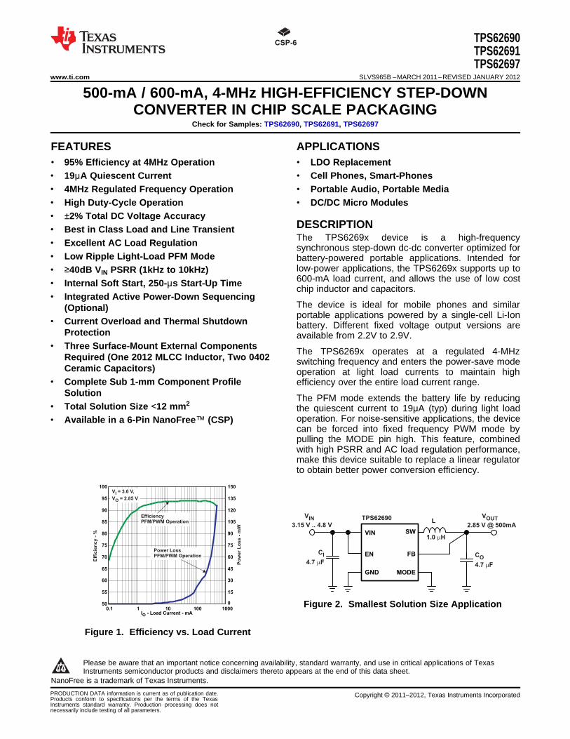
CSP-6 VIN SW FB MODE EN GND V OUT 2.85 V @ 500mA C 4.7 F I m TPS62690 L 1.0 H m C 4.7 F O m V IN 3.15 V .. 4.8 V 50 55 60 65 70 75 80 85 90 95 100 0.1 1 10 100 1000 0 15 30 45 60 75 90 105 120 135 150 I - Load Current - mA O Efficiency - % Power Loss - mW V = 3.6 V, V = 2.85 V I O Efficiency PFM/PWM Operation Power Loss PFM/PWM Operation TPS62690 TPS62691 TPS62697 www.ti.com SLVS965B – MARCH 2011 – REVISED JANUARY 2012 500-mA / 600-mA, 4-MHz HIGH-EFFICIENCY STEP-DOWN CONVERTER IN CHIP SCALE PACKAGING Check for Samples: TPS62690, TPS62691, TPS62697 1FEATURES APPLICATIONS 2• 95% Efficiency at 4MHz Operation • LDO Replacement • 19μA Quiescent Current • Cell Phones, Smart-Phones • 4MHz Regulated Frequency Operation • Portable Audio, Portable Media • High Duty-Cycle Operation • DC/DC Micro Modules • ±2% Total DC Voltage Accuracy DESCRIPTION • Best in Class Load and Line Transient The TPS6269x device is a high-frequency • Excellent AC Load Regulation synchronous step-down dc-dc converter optimized for • Low Ripple Light-Load PFM Mode battery-powered portable applications. Intended for low-power applications, the TPS6269x supports up to • ≥40dB V IN PSRR (1kHz to 10kHz) 600-mA load current, and allows the use of low cost • Internal Soft Start, 250-μs Start-Up Time chip inductor and capacitors. • Integrated Active Power-Down Sequencing The device is ideal for mobile phones and similar (Optional) portable applications powered by a single-cell Li-Ion • Current Overload and Thermal Shutdown battery. Different fixed voltage output versions are Protection available from 2.2V to 2.9V. • Three Surface-Mount External Components The TPS6269x operates at a regulated 4-MHz Required (One 2012 MLCC Inductor, Two 0402 switching frequency and enters the power-save mode Ceramic Capacitors) operation at light load currents to maintain high • Complete Sub 1-mm Component Profile efficiency over the entire load current range. Solution The PFM mode extends the battery life by reducing • Total Solution Size <12 mm 2 the quiescent current to 19μA (typ) during light load operation. For noise-sensitive applications, the device • Available in a 6-Pin NanoFree™ (CSP) can be forced into fixed frequency PWM mode by pulling the MODE pin high. This feature, combined with high PSRR and AC load regulation performance, make this device suitable to replace a linear regulator to obtain better power conversion efficiency. Figure 2. Smallest Solution Size Application Figure 1. Efficiency vs. Load Current 1 Please be aware that an important notice concerning availability, standard warranty, and use in critical applications of Texas Instruments semiconductor products and disclaimers thereto appears at the end of this data sheet. 2NanoFree is a trademark of Texas Instruments. PRODUCTION DATA information is current as of publication date. Copyright © 2011–2012, Texas Instruments Incorporated Products conform to specifications per the terms of the Texas Instruments standard warranty. Production processing does not necessarily include testing of all parameters.
Transcript of SLVS965B MARCH 2011 REVISED JANUARY 2012 500 … · • ≥40dB V low-power applications, ......
CSP-6
VIN SW
FB
MODE
EN
GND
VOUT
2.85 V @ 500mA
C
4.7 F
I
m
TPS62690 L
1.0 Hm
C
4.7 F
O
m
VIN
3.15 V .. 4.8 V
50
55
60
65
70
75
80
85
90
95
100
0.1 1 10 100 10000
15
30
45
60
75
90
105
120
135
150
I - Load Current - mAO
Eff
icie
nc
y -
%
Po
we
r L
os
s -
mW
V = 3.6 V,
V = 2.85 VI
O
EfficiencyPFM/PWM Operation
Power LossPFM/PWM Operation
TPS62690TPS62691TPS62697
www.ti.com SLVS965B –MARCH 2011–REVISED JANUARY 2012
500-mA / 600-mA, 4-MHz HIGH-EFFICIENCY STEP-DOWNCONVERTER IN CHIP SCALE PACKAGING
Check for Samples: TPS62690, TPS62691, TPS62697
1FEATURES APPLICATIONS2• 95% Efficiency at 4MHz Operation • LDO Replacement• 19μA Quiescent Current • Cell Phones, Smart-Phones• 4MHz Regulated Frequency Operation • Portable Audio, Portable Media• High Duty-Cycle Operation • DC/DC Micro Modules• ±2% Total DC Voltage Accuracy
DESCRIPTION• Best in Class Load and Line TransientThe TPS6269x device is a high-frequency• Excellent AC Load Regulation synchronous step-down dc-dc converter optimized for
• Low Ripple Light-Load PFM Mode battery-powered portable applications. Intended forlow-power applications, the TPS6269x supports up to• ≥40dB VIN PSRR (1kHz to 10kHz)600-mA load current, and allows the use of low cost• Internal Soft Start, 250-μs Start-Up Timechip inductor and capacitors.
• Integrated Active Power-Down SequencingThe device is ideal for mobile phones and similar(Optional)portable applications powered by a single-cell Li-Ion
• Current Overload and Thermal Shutdown battery. Different fixed voltage output versions areProtection available from 2.2V to 2.9V.
• Three Surface-Mount External ComponentsThe TPS6269x operates at a regulated 4-MHz
Required (One 2012 MLCC Inductor, Two 0402 switching frequency and enters the power-save modeCeramic Capacitors) operation at light load currents to maintain high
• Complete Sub 1-mm Component Profile efficiency over the entire load current range.Solution The PFM mode extends the battery life by reducing
• Total Solution Size <12 mm2the quiescent current to 19μA (typ) during light loadoperation. For noise-sensitive applications, the device• Available in a 6-Pin NanoFree™ (CSP)can be forced into fixed frequency PWM mode bypulling the MODE pin high. This feature, combinedwith high PSRR and AC load regulation performance,make this device suitable to replace a linear regulatorto obtain better power conversion efficiency.
Figure 2. Smallest Solution Size Application
Figure 1. Efficiency vs. Load Current
1
Please be aware that an important notice concerning availability, standard warranty, and use in critical applications of TexasInstruments semiconductor products and disclaimers thereto appears at the end of this data sheet.
2NanoFree is a trademark of Texas Instruments.
PRODUCTION DATA information is current as of publication date. Copyright © 2011–2012, Texas Instruments IncorporatedProducts conform to specifications per the terms of the TexasInstruments standard warranty. Production processing does notnecessarily include testing of all parameters.
TPS62690TPS62691TPS62697SLVS965B –MARCH 2011–REVISED JANUARY 2012 www.ti.com
These devices have limited built-in ESD protection. The leads should be shorted together or the device placed in conductive foamduring storage or handling to prevent electrostatic damage to the MOS gates.
ORDERING INFORMATION (1)
PACKAGEPART OUTPUT DEVICETA ORDERING (3) MARKINGNUMBER VOLTAGE (2) SPECIFIC FEATURE CHIP CODE
TPS62690 2.85V 500mA peak output current TPS62690YFF PB
-40°C to 85°C TPS62691 (4) 2.2V 600mA peak output current TPS62691YFF SU
TPS62697 2.8V 500mA peak output current TPS62697YFF WA
(1) For the most current package and ordering information, see the Package Option Addendum at the end of this document, or see the TIwebsite at www.ti.com.
(2) Internal tap points are available to facilitate output voltages in 25mV increments.(3) The YFF package is available in tape and reel. Add a R suffix (e.g. TPS62690YFFR) to order quantities of 3000 parts. Add a T suffix
(e.g. TPS62690YFFT) to order quantities of 250 parts.(4) Product preview. Contact TI factory for more information.
ABSOLUTE MAXIMUM RATINGSover operating free-air temperature range (unless otherwise noted) (1)
MIN MAX UNIT
Voltage at VIN (2) (3), SW(3) –0.3 6 V
Input Voltage Voltage at FB (3) –0.3 3.6 V
Voltage at EN, MODE (3) –0.3 VI + 0.3 V
TPS62690, 500 mATPS62697Peak output current, IOTPS62691 600 mA
Power dissipation Internally limited
Operating temperature range, TA(4) –40 85 °C
Operating junction temperature, TJ 150 °CStorage temperature range, Tstg –65 150 °C
Human body model 2 kV
ESD (5) Charge device model 1 kV
Machine model 200 V
(1) Stresses beyond those listed under absolute maximum ratings may cause permanent damage to the device. These are stress ratingsonly and functional operation of the device at these or any other conditions beyond those indicated under recommended operatingconditions is not implied. Exposure to absolute-maximum-rated conditions for extended periods may affect device reliability.
(2) Operation above 4.8V input voltage is not recommended over an extended period of time.(3) All voltage values are with respect to network ground terminal.(4) In applications where high power dissipation and/or poor package thermal resistance is present, the maximum ambient temperature may
have to be derated. Maximum ambient temperature (TA(max)) is dependent on the maximum operating junction temperature (TJ(max)), themaximum power dissipation of the device in the application (PD(max)), and the junction-to-ambient thermal resistance of the part/packagein the application (θJA), as given by the following equation: TA(max)= TJ(max)–(θJA X PD(max)). To achieve optimum performance, it isrecommended to operate the device with a maximum junction temperature of 105°C.
(5) The human body model is a 100-pF capacitor discharged through a 1.5-kΩ resistor into each pin. The machine model is a 200-pFcapacitor discharged directly into each pin.
THERMAL INFORMATIONTPS62690
THERMAL METRIC (1) UNITSYFF (6 PINS)
θJA Junction-to-ambient thermal resistance 133.2
θJCtop Junction-to-case (top) thermal resistance 1.4
θJB Junction-to-board thermal resistance 22.5°C/W
ψJT Junction-to-top characterization parameter 5.5
ψJB Junction-to-board characterization parameter 22.3
θJCbot Junction-to-case (bottom) thermal resistance -
(1) For more information about traditional and new thermal metrics, see the IC Package Thermal Metrics application report, SPRA953.
2 Submit Documentation Feedback Copyright © 2011–2012, Texas Instruments Incorporated
Product Folder Link(s): TPS62690 TPS62691 TPS62697
TPS62690TPS62691TPS62697
www.ti.com SLVS965B –MARCH 2011–REVISED JANUARY 2012
RECOMMENDED OPERATING CONDITIONSMIN NOM MAX UNIT
VIN Input voltage range 2.3 4.8 (1) V
TPS62690, 0 500 mATPS62697IO Output current rangeTPS62691 0 600 mA
L Inductance 0.5 1.8 µH
CO Output capacitance 1 5 10 µF
TA Ambient temperature –40 +85 °CTJ Operating junction temperature –40 +125 °C
(1) Operation above 4.8V input voltage is not recommended over an extended period of time.
ELECTRICAL CHARACTERISTICSMinimum and maximum values are at VIN = 2.3V to 5.5V, VOUT = 2.85V, EN = 1.8V, AUTO mode and TA = –40°C to 85°C;Circuit of Parameter Measurement Information section (unless otherwise noted). Typical values are at VIN = 3.6V, VOUT =2.85V, EN = 1.8V, AUTO mode and TA = 25°C (unless otherwise noted).
PARAMETER TEST CONDITIONS MIN TYP MAX UNIT
SUPPLY CURRENT
TPS6269x IO = 0mA. Device not switching 19 50 μAOperating quiescentIQ current TPS6269x IO = 0mA, PWM mode 4.2 mA
I(SD) Shutdown current TPS6269x EN = GND 0.2 5 μA
Undervoltage lockoutUVLO TPS6269x 2.05 2.1 Vthreshold
ENABLE, MODE
VIH High-level input voltage 1 V
VIL Low-level input voltage TPS6269x 0.4 V
Ilkg Input leakage current Input connected to GND or VIN 0.01 1.5 μA
POWER SWITCH
VIN = V(GS) = 3.6V. PWM mode 160 280 (1) mΩP-channel MOSFET onrDS(on) TPS6269xresistance VIN = V(GS) = 2.9V. PWM mode 190 350 (1) mΩ
P-channel leakageIlkg TPS6269x V(DS) = 5.5V, -40°C ≤ TJ ≤ 85°C 1 μAcurrent, PMOS
VIN = V(GS) = 3.6V. PWM mode 110 mΩN-channel MOSFET onrDS(on) TPS6269xresistance VIN = V(GS) = 2.9V. PWM mode 140 mΩ
N-channel leakageIlkg TPS6269x V(DS) = 5.5V, -40°C ≤ TJ ≤ 85°C 2 μAcurrent, NMOS
Discharge resistor forrDIS 100 150 Ωpower-down sequence
2.3V ≤ VIN ≤ 4.8V. Open loop 900 1100 1250 mATPS62690TPS62697P-MOS current limit VIN = 3.6V. Closed loop 830 mA
TPS62691 2.3V ≤ VIN ≤ 4.8V. Open loop 1050 1250 1400 mA
Input current limit under TPS6269x VO shorted to ground 15 mAshort-circuit conditions
Thermal shutdown 140 °CTPS6269xThermal shutdown 10 °Chysteresis
(1) Verified by characterization. Not tested in production.
Copyright © 2011–2012, Texas Instruments Incorporated Submit Documentation Feedback 3
Product Folder Link(s): TPS62690 TPS62691 TPS62697
TPS62690TPS62691TPS62697SLVS965B –MARCH 2011–REVISED JANUARY 2012 www.ti.com
ELECTRICAL CHARACTERISTICS (continued)Minimum and maximum values are at VIN = 2.3V to 5.5V, VOUT = 2.85V, EN = 1.8V, AUTO mode and TA = –40°C to 85°C;Circuit of Parameter Measurement Information section (unless otherwise noted). Typical values are at VIN = 3.6V, VOUT =2.85V, EN = 1.8V, AUTO mode and TA = 25°C (unless otherwise noted).
PARAMETER TEST CONDITIONS MIN TYP MAX UNIT
OSCILLATOR
fSW Oscillator frequency TPS6269x IO = 0mA, PWM mode. TA = 25°C 3.6 4 4.4 MHz
OUTPUT
3.15V ≤ VIN ≤ 4.8V, 0mA ≤ IO ≤ 500 mA 0.98×VNOM VNOM 1.03×VNOM VPFM/PWM operation
Regulated DC output 3.15V ≤ VIN ≤ 5.5V, 0mA ≤ IO ≤ 500 mA 0.98×VNOM VNOM 1.04×VNOM Vvoltage PFM/PWM operationTPS62690 3.15V ≤ VIN ≤ 5.5V, 0mA ≤ IO ≤ 500 mATPS62697 0.98×VNOM VNOM 1.02×VNOM VVOUT PWM operation
VIN = VO + 0.5V (min 3.15V) to 5.5VLine regulation 0.18 %/VIO = 200 mA
Load regulation IO = 0mA to 500 mA –0.0002 %/mA
Load regulation IO = 0mA to 500 mA –0.0002 %/mA
2.9 V ≤ VIN ≤ 4.8V, 0mA ≤ IO ≤ 600 mA 0.98×VNOM VNOM 1.03×VNOM VPFM/PWM operation
Regulated DC output 2.65V ≤ VIN ≤ 4.8V, 0mA ≤ IO ≤ 600 mA 0.97×VNOM VNOM 1.03×VNOM Vvoltage PFM/PWM operation
VOUT TPS62691 2.65V ≤ VIN ≤ 5.5V, 0mA ≤ IO ≤ 600 mA 0.97×VNOM VNOM 1.02×VNOM VPWM operation
VIN = VO + 0.5V (min 2.5V) to 5.5VLine regulation 0.12 %/VIO = 200 mA
Load regulation IO = 0mA to 600 mA –0.0003 %/mA
Feedback input TPS6269x 480 kΩresistance
IO = 1mA 65 mVPPCO = 4.7μF X5R 6.3V 0402TPS62690TPS62697Power-save mode ripple IO = 1mAΔVO 25 mVPPvoltage CO = 10μF X5R 6.3V 0603
IO = 1mATPS62691 22 mVPPCO = 10μF X5R 6.3V 0603
TPS62690 IO = 0mA, Time from active EN to VO 250 μsTPS62697Start-up timeTPS62691 IO = 0mA, Time from active EN to VO 205 μs
4 Submit Documentation Feedback Copyright © 2011–2012, Texas Instruments Incorporated
Product Folder Link(s): TPS62690 TPS62691 TPS62697
GND
A1
B1
C1
A2
B2
C2FB
SW
MODE VIN
EN
TPS6269xCSP-6
(TOP VIEW)
MODE
C1
A2
B2
C2
A1
B1
VIN
EN
GND FB
SW
TPS6269xCSP-6
(BOTTOM VIEW)
TPS62690TPS62691TPS62697
www.ti.com SLVS965B –MARCH 2011–REVISED JANUARY 2012
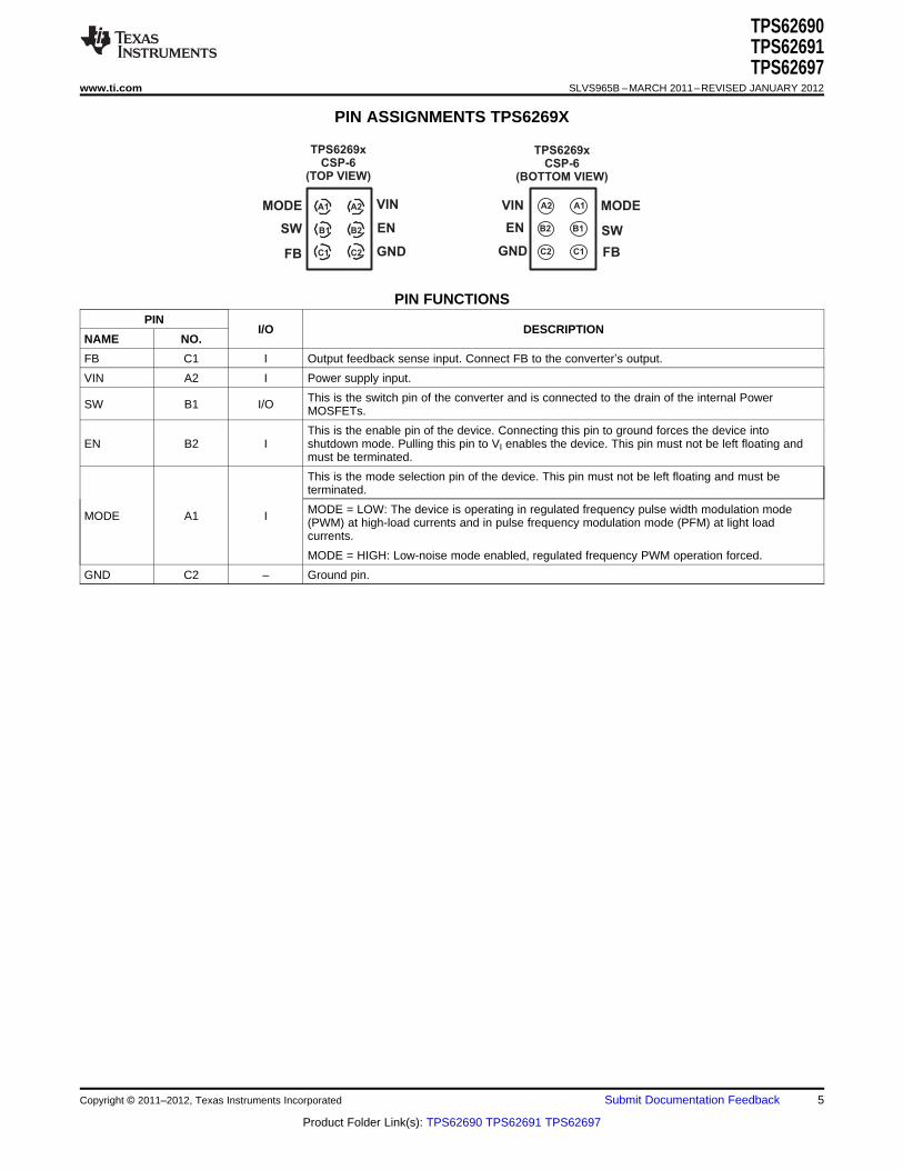
PIN ASSIGNMENTS TPS6269X
PIN FUNCTIONSPIN
I/O DESCRIPTIONNAME NO.
FB C1 I Output feedback sense input. Connect FB to the converter’s output.
VIN A2 I Power supply input.
This is the switch pin of the converter and is connected to the drain of the internal PowerSW B1 I/O MOSFETs.
This is the enable pin of the device. Connecting this pin to ground forces the device intoEN B2 I shutdown mode. Pulling this pin to VI enables the device. This pin must not be left floating and
must be terminated.
This is the mode selection pin of the device. This pin must not be left floating and must beterminated.
MODE = LOW: The device is operating in regulated frequency pulse width modulation modeMODE A1 I (PWM) at high-load currents and in pulse frequency modulation mode (PFM) at light loadcurrents.
MODE = HIGH: Low-noise mode enabled, regulated frequency PWM operation forced.
GND C2 – Ground pin.
Copyright © 2011–2012, Texas Instruments Incorporated Submit Documentation Feedback 5
Product Folder Link(s): TPS62690 TPS62691 TPS62697
Gate Driver
Anti
Shoot-Through
Power Save Mode
Switching Logic
+
-
Frequency
Control
FB
R1
R2
SW
GND
Soft-Start
EN VIN
Current Limit
Detect
UndervoltageLockout
Bias Supply
Bandgap
Thermal
Shutdown
Negative Inductor
Current Detect
VIN
MODE
V = 0.8 VREF
VREF
VIN SW
FB
MODE
EN
GND
L
VIN CI
TPS6269x
CO
VOUT
TPS62690TPS62691TPS62697SLVS965B –MARCH 2011–REVISED JANUARY 2012 www.ti.com
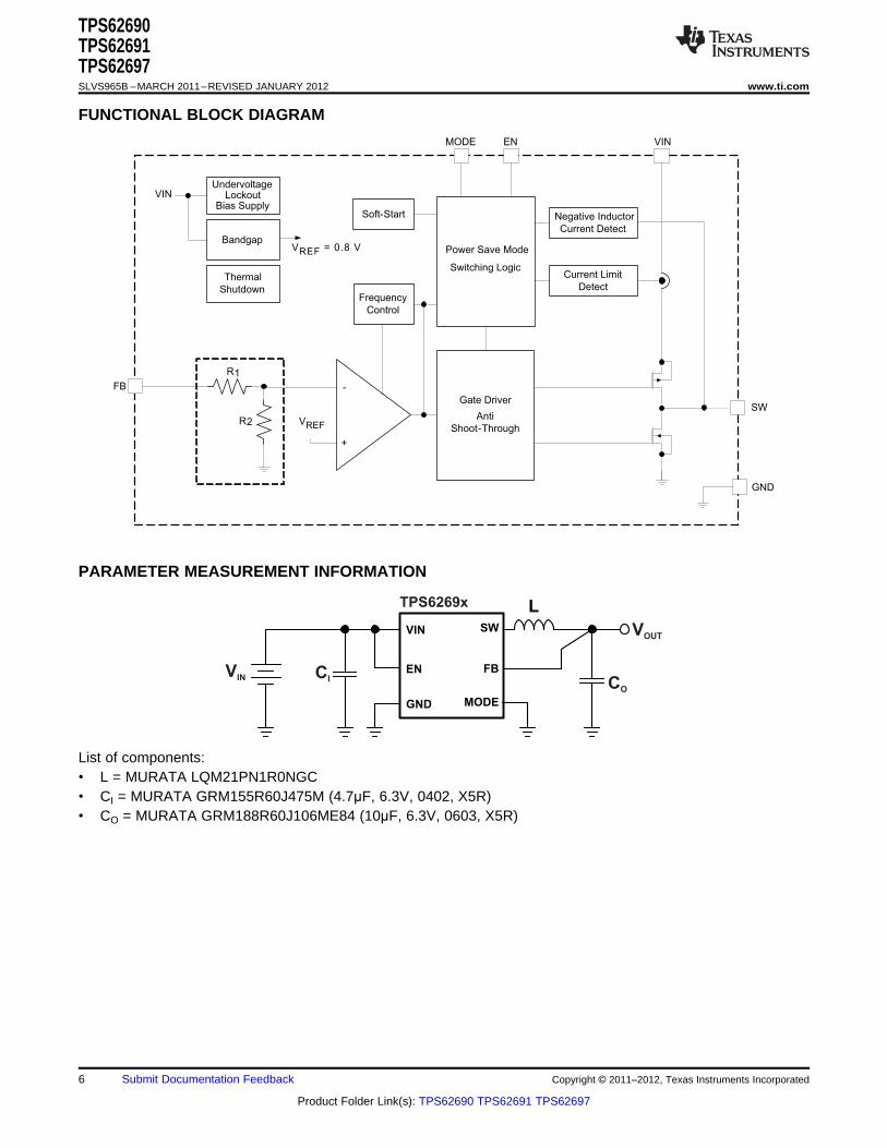
FUNCTIONAL BLOCK DIAGRAM
PARAMETER MEASUREMENT INFORMATION
List of components:• L = MURATA LQM21PN1R0NGC• CI = MURATA GRM155R60J475M (4.7μF, 6.3V, 0402, X5R)• CO = MURATA GRM188R60J106ME84 (10μF, 6.3V, 0603, X5R)
6 Submit Documentation Feedback Copyright © 2011–2012, Texas Instruments Incorporated
Product Folder Link(s): TPS62690 TPS62691 TPS62697
0
10
20
30
40
50
60
70
80
90
100
0.1 1 10 100 1000
V = 3 V
PFM/PWM OperationI
I - Load Current - mAO
Eff
icie
ncy -
%
V = 3.2 V
PFM/PWM OperationI
V = 3.6 V
PFM/PWM OperationI
V = 4.2 V
PFM/PWM OperationI
V = 3.6 V
Forced PWM OperationI
V = 2.85 VO
1 10 100 10000
10
20
30
40
50
60
70
80
90
100
Eff
icie
nc
y -
%
I - Load Current - mAO
V = 3.2 V
Forced PWMI
V = 2.85 VO
V = 3.6 V
Forced PWMI
V = 4.2 V
Forced PWMI
V = 3 V
Forced PWMI
TPS62690TPS62691TPS62697
www.ti.com SLVS965B –MARCH 2011–REVISED JANUARY 2012
TYPICAL CHARACTERISTICS
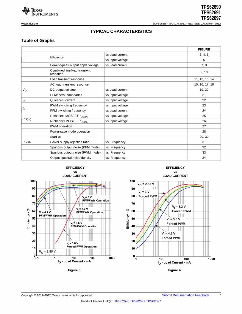
Table of Graphs
FIGURE
vs Load current 3, 4, 5η Efficiency
vs Input voltage 6
Peak-to-peak output ripple voltage vs Load current 7, 8
Combined line/load transient 9, 10response
Load transient response 11, 12, 13, 14
AC load transient response 15, 16, 17, 18
VO DC output voltage vs Load current 19, 20
PFM/PWM boundaries vs Input voltage 21
IQ Quiescent current vs Input voltage 22
PWM switching frequency vs Input voltage 23fs
PFM switching frequency vs Load current 24
P-channel MOSFET rDS(on) vs Input voltage 25rDS(on)
N-channel MOSFET rDS(on) vs Input voltage 26
PWM operation 27
Power-save mode operation 28
Start-up 29, 30
PSRR Power supply rejection ratio vs. Frequency 31
Spurious output noise (PFM mode) vs. Frequency 32
Spurious output noise (PWM mode) vs. Frequency 33
Output spectral noise density vs. Frequency 34
EFFICIENCY EFFICIENCYvs vs
LOAD CURRENT LOAD CURRENT
Figure 3. Figure 4.
Copyright © 2011–2012, Texas Instruments Incorporated Submit Documentation Feedback 7
Product Folder Link(s): TPS62690 TPS62691 TPS62697

0
10
20
30
40
50
60
70
80
90
100
0.1 10 100 1000I - Load Current - mAO
Eff
icie
ncy -
%
V = 3.6 V
PFM/PWM OperationI
1
V = 4.2 V
PFM/PWM OperationI
V = 2.2 VO
V = 3.2 V
PFM/PWM OperationI
V = 2.7 V
PFM/PWM OperationI
2.9 3.1 3.3 3.5 3.7 3.9 4.1 4.3 4.5 4.7V - Input Voltage - VI
82
84
86
88
90
92
94
96
98
100
Eff
icie
nc
y -
%
I = 100 mAO
I = 10 mAO
I = 300 mAO
I = 1 mAO
V = 2.85 V,
PFM/PWM OperationO
0
5
10
15
20
25
30
35
40
45
0 50 100 150 200 250 300 350
I - Load Current - mAO
V-
Peak-t
o-P
eak O
utp
ut
Rip
ple
Vo
ltag
e -
mV
O
V = 2.85 V,
C = 10 F
O
O m
PFM/PWM Operation
V = 4.5 VI
V = 3.3 VI
V = 3.6 VI
400 450 500 0 50 100 150 200 250 300 350I - Load Current - mAO
0
10
20
30
40
50
60
70
80
90
100
110
V-
Peak-t
o-P
eak O
utp
ut
Rip
ple
Vo
ltag
e -
mV
O
V = 3.2 VI
V = 4.5 VI
V = 3.6 VI
V = 2.85 V,
C = 4.7 F
O
O m
PFM/PWM Operation
TPS62690TPS62691TPS62697SLVS965B –MARCH 2011–REVISED JANUARY 2012 www.ti.com
TYPICAL CHARACTERISTICS (continued)EFFICIENCY EFFICIENCY
vs vsLOAD CURRENT INPUT VOLTAGE
Figure 5. Figure 6.
PEAK-TO-PEAK OUTPUT RIPPLE VOLTAGE PEAK-TO-PEAK OUTPUT RIPPLE VOLTAGEvs vs
LOAD CURRENT LOAD CURRENT
Figure 7. Figure 8.
8 Submit Documentation Feedback Copyright © 2011–2012, Texas Instruments Incorporated
Product Folder Link(s): TPS62690 TPS62691 TPS62697
3.3V to 3.9V mA Line Step
V = 2.85 VO
MODE = Low
10 to 400 mA Load Step
3.15V to 3.75V mA Line Step
V = 2.85 VO
MODE = Low
10 to 400 mA Load Step
MODE = Low
V = 3.6 V,
V = 2.85 VI
O
5 to 200 mA Load Step
10 to 400 mA Load Step
V = 3.6 V,
V = 2.85 VI
O
MODE = Low
TPS62690TPS62691TPS62697
www.ti.com SLVS965B –MARCH 2011–REVISED JANUARY 2012
TYPICAL CHARACTERISTICS (continued)
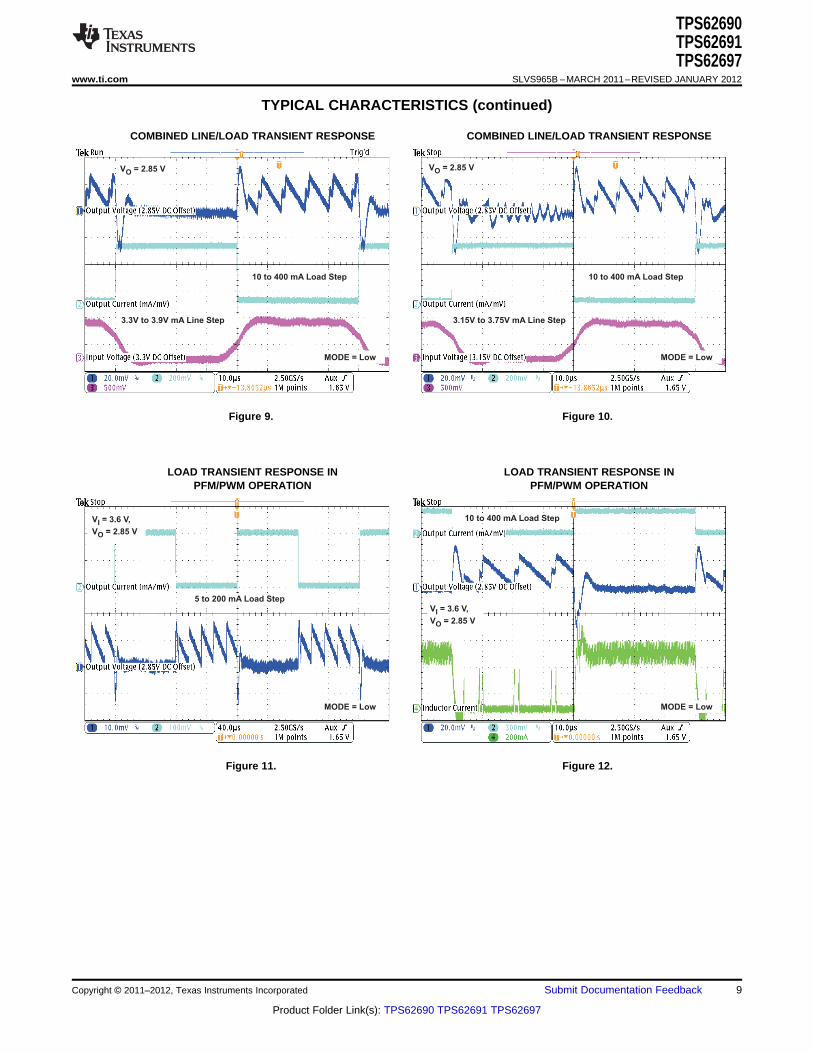
COMBINED LINE/LOAD TRANSIENT RESPONSE COMBINED LINE/LOAD TRANSIENT RESPONSE
Figure 9. Figure 10.
LOAD TRANSIENT RESPONSE IN LOAD TRANSIENT RESPONSE INPFM/PWM OPERATION PFM/PWM OPERATION
Figure 11. Figure 12.
Copyright © 2011–2012, Texas Instruments Incorporated Submit Documentation Feedback 9
Product Folder Link(s): TPS62690 TPS62691 TPS62697
10 to 400 mA Load Step
V = 3.15 V,
V = 2.85 VI
O
MODE = Low
10 to 400 mA Load Step
V = 4.8 V,
V = 2.85 VI
O
MODE = Low
MODE = Low
V = 3.05 V,
V = 2.85 VI
O
5 to 600 mA Load Sweep
MODE = Low
V = 3.15 V,
V = 2.85 VI
O
5 to 500 mA Load Sweep
TPS62690TPS62691TPS62697SLVS965B –MARCH 2011–REVISED JANUARY 2012 www.ti.com
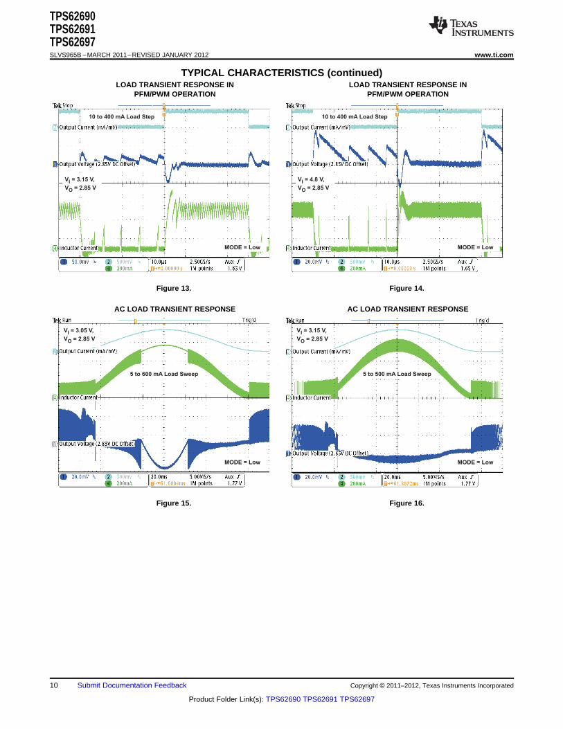
TYPICAL CHARACTERISTICS (continued)LOAD TRANSIENT RESPONSE IN LOAD TRANSIENT RESPONSE IN
PFM/PWM OPERATION PFM/PWM OPERATION
Figure 13. Figure 14.
AC LOAD TRANSIENT RESPONSE AC LOAD TRANSIENT RESPONSE
Figure 15. Figure 16.
10 Submit Documentation Feedback Copyright © 2011–2012, Texas Instruments Incorporated
Product Folder Link(s): TPS62690 TPS62691 TPS62697
MODE = Low
V = 3.6 V,
V = 2.85 VI
O
5 to 500 mA Load Sweep
MODE = Low
V = 4.2 V,
V = 2.85 VI
O
5 to 500 mA Load Sweep
0.1 1 10 100 1000I - Load Current - mAO
2.765
2.793
2.822
2.850
2.879
2.907
V-
Ou
tpu
t V
olt
ag
e -
VO
V = 2.85 V,
PFM/PWM OperationO
V = 3.2 V, T = 25°CI A
V = 3.1 V, T = 85°CI A
V = 3.0 V, T = 85°CI A
V = 2.9 V, T = 25°CI A
0.1 1 10 100 1000I - Load Current - mAO
2.765
2.793
2.822
2.850
2.879
2.907
V-
Ou
tpu
t V
olt
ag
e -
VO
V = 2.85 V,
PFM/PWM OperationO
V = 3.2 VIV = 4.5 VI
V = 3.6 VI
V = 2.9 VI
TPS62690TPS62691TPS62697
www.ti.com SLVS965B –MARCH 2011–REVISED JANUARY 2012
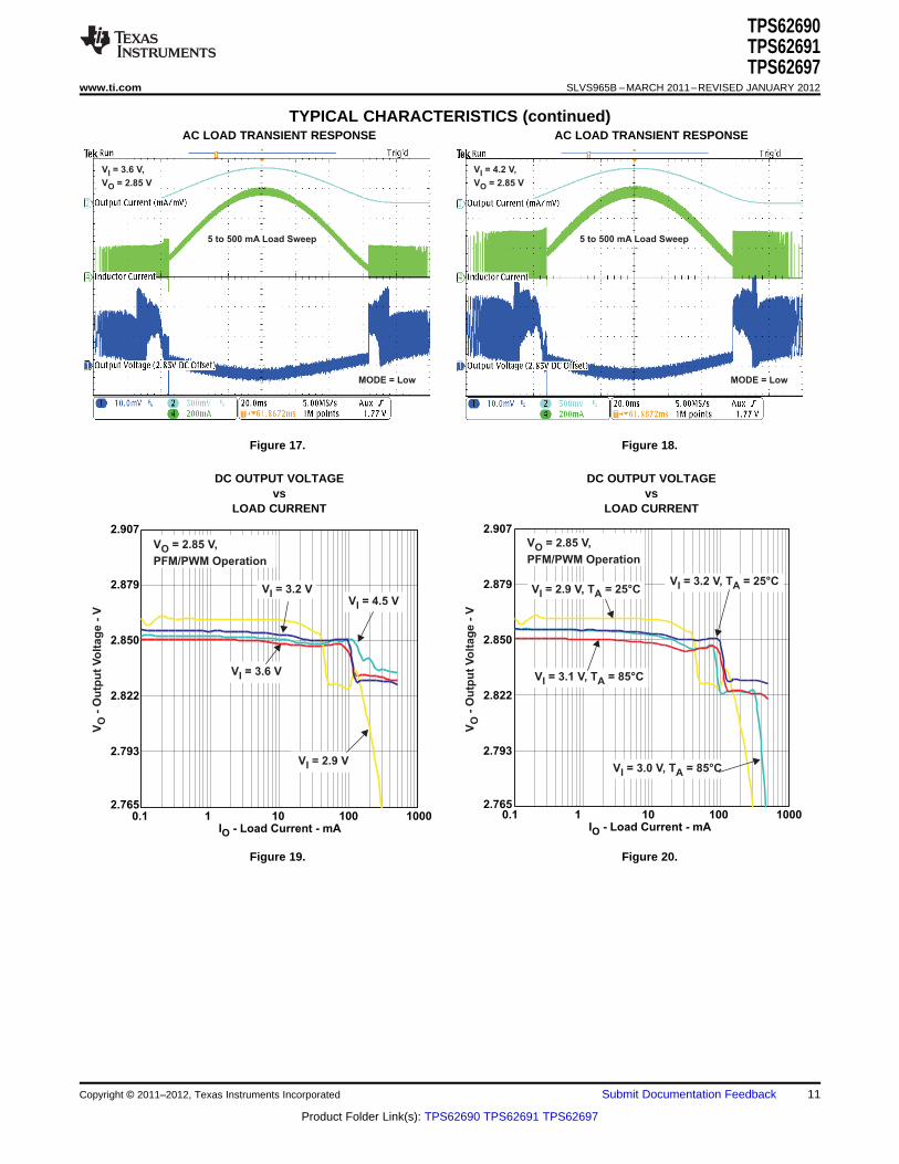
TYPICAL CHARACTERISTICS (continued)AC LOAD TRANSIENT RESPONSE AC LOAD TRANSIENT RESPONSE
Figure 17. Figure 18.
DC OUTPUT VOLTAGE DC OUTPUT VOLTAGEvs vs
LOAD CURRENT LOAD CURRENT
Figure 19. Figure 20.
Copyright © 2011–2012, Texas Instruments Incorporated Submit Documentation Feedback 11
Product Folder Link(s): TPS62690 TPS62691 TPS62697

0
20
40
60
80
100
120
140
160
180
200
220
240
3.1 3.4 3.6 4.0 4.2 4.6 4.8
V - Input Voltage - VI
I-
Lo
ad
Cu
rren
t -
mA
O
V = 2.85 VO
Always PWM
PWM to PFMMode Change
The switching modechanges at these borders
Always PFM
PFM to PWMMode Change
3.2 3.8 4.4 2.7 3 3.3 3.6 3.9 4.2 4.5 4.8V - Input Voltage - VI
T = 85°CA
T = 25°CA
T = -40°CA
0
2
4
6
8
10
12
14
16
18
20
22
24
26
28
30
32
34
36
38
I-
Qu
iescen
t C
urr
en
t -
AQ
m
1.6
1.8
2
2.2
2.4
2.6
2.8
3
3.2
3.4
3.6
3.8
4
4.2
2.9 3.1 3.3 3.5 3.7 3.9 4.1 4.3 4.5V - Input Voltage - VI
I = 500 mAO
I = 400 mAO
I = 300 mAO
I = 150 mAO
I = 50 mAO
f-
Sw
itc
hin
g F
req
ue
nc
y -
MH
zs
V = 2.85 V
MODE = HighO
0
0.5
1
1.5
2
2.5
3
3.5
4
4.5
0 20 40 60 80 100 120 140 160 180 200 220 240
I - Load Current - mAO
f-
Sw
itc
hin
g F
req
ue
nc
y -
MH
zS
V = 4.5 VI
V = 3.2 VI
V = 3.6 VI
V = 2.85 V
MODE = LowO
TPS62690TPS62691TPS62697SLVS965B –MARCH 2011–REVISED JANUARY 2012 www.ti.com
TYPICAL CHARACTERISTICS (continued)QUIESCENT CURRENT
vsPFM/PWM BOUNDARIES INPUT VOLTAGE
Figure 21. Figure 22.
PWM SWITCHING FREQUENCY PFM SWITCHING FREQUENCYvs vs
INPUT VOLTAGE INPUT VOLTAGE
Figure 23. Figure 24.
12 Submit Documentation Feedback Copyright © 2011–2012, Texas Instruments Incorporated
Product Folder Link(s): TPS62690 TPS62691 TPS62697

0
25
50
75
100
125
150
175
200
225
250
2.7 3 3.3 3.6 3.9 4.2 4.5 4.8
V - Input Voltage - VI
r-
Sta
tic
Dra
in-S
ou
rce
On
-Re
sis
tan
ce
- m
DS
(on
)W
T = 25°CA
T = 85°CA
T = -40°CA
75
100
125
150
175
200
225
250
275
2.7 3 3.3 3.6 3.9 4.2 4.5 4.8V - Input Voltage - VI
T = 25°CA
T = 85°CA
T = -40°CA
r-
Sta
tic D
rain
-So
urc
e O
n-R
esis
tan
ce -
mD
S(o
n)
W
MODE = Low
V = 3.6 V,
V = 2.85 V,
I
I
O
O = 150 mA
MODE = Low
V = 3.6 V, V = 2.85V, II O O = 60 mA
TPS62690TPS62691TPS62697
www.ti.com SLVS965B –MARCH 2011–REVISED JANUARY 2012
TYPICAL CHARACTERISTICS (continued)P-CHANNEL rDS(ON) N-CHANNEL rDS(ON)
vs vsINPUT VOLTAGE INPUT VOLTAGE
Figure 25. Figure 26.
PWM OPERATION POWER-SAVE MODE OPERATION
Figure 27. Figure 28.
Copyright © 2011–2012, Texas Instruments Incorporated Submit Documentation Feedback 13
Product Folder Link(s): TPS62690 TPS62691 TPS62697

MODE = Low
V = 3.6 V,
V = 2.85 V,I
O
I = 0 mAO
MODE = Low
V = 3.6 V,
V = 2.85 V,I
O
R = 39L W
0.01 0.1 1 10 100 1000f - Frequency - kHz
0
5
10
15
20
25
30
35
40
45
50
55
60
65
70
75
80
85
PS
RR
- P
ow
er
Su
pp
ly R
eje
cti
on
Ra
tio
- d
B
I = 400 mA
PWM OperationO
I = 250 mA
PWM OperationO
I = 20 mA
PWM OperationO
I = 20 mA
PFM OperationO
V = 3.6 VI
V = 2.85 VO
0 5
7 m
6 m
5 m
4 m
3 m
2 m
1 m
100 n
Sp
uri
ou
s O
utp
ut
No
ise
(P
FM
Mo
de
) -
V
f - Frequency - MHz
Span = 500 kHz
8 m
9 m
10 m
V = 2.85 V
R = 150O
L Ω
V = 3.2 VI
V = 3.6 VI
V = 4.2 VI
TPS62690TPS62691TPS62697SLVS965B –MARCH 2011–REVISED JANUARY 2012 www.ti.com
TYPICAL CHARACTERISTICS (continued)START-UP START-UP
Figure 29. Figure 30.
POWER SUPPLY REJECTION RATIO SPURIOUS OUTPUT NOISE (PFM MODE)vs vs
FREQUENCY FREQUENCY
Figure 31. Figure 32.
14 Submit Documentation Feedback Copyright © 2011–2012, Texas Instruments Incorporated
Product Folder Link(s): TPS62690 TPS62691 TPS62697
0.01
0.1
1
10
100
0.1 1 10 100 1000f - Frequency - kHz
I = 2 mA
PFM OperationOUT
I = 20 mA
PFM OperationOUT
V = 3.6 V,
V = 2.85 VIN
OUT
ÖO
utp
ut
Sp
ec
tra
l N
ois
e D
en
sit
y -
µV
/
Hz
I = 250 mA
PWM OperationOUT
0 20
700 µ
600 µ
500 µ
400 µ
300 µ
200 µ
100 µ
100 n
Sp
uri
ou
s O
utp
ut
No
ise
(P
WM
Mo
de
) -
V
f - Frequency - MHz
Span = 2 MHz
800 µ
900 µ
1 m
V = 2.85 V
R = 12O
L Ω
V = 3.2 VI
V = 4.2 VI
V = 3.6 VI
TPS62690TPS62691TPS62697
www.ti.com SLVS965B –MARCH 2011–REVISED JANUARY 2012
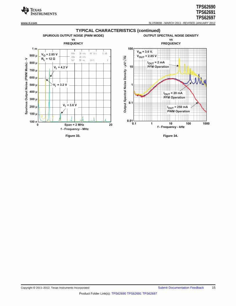
TYPICAL CHARACTERISTICS (continued)SPURIOUS OUTPUT NOISE (PWM MODE) OUTPUT SPECTRAL NOISE DENSITY
vs vsFREQUENCY FREQUENCY
Figure 33. Figure 34.
Copyright © 2011–2012, Texas Instruments Incorporated Submit Documentation Feedback 15
Product Folder Link(s): TPS62690 TPS62691 TPS62697
TPS62690TPS62691TPS62697SLVS965B –MARCH 2011–REVISED JANUARY 2012 www.ti.com
DETAILED DESCRIPTION
OPERATION
The TPS6269x is a synchronous step-down converter typically operates at a regulated 4-MHz frequency pulsewidth modulation (PWM) at moderate to heavy load currents. At light load currents, the TPS6269x converteroperates in power-save mode with pulse frequency modulation (PFM).
The converter uses a unique frequency locked ring oscillating modulator to achieve best-in-class load and lineresponse and allows the use of tiny inductors and small ceramic input and output capacitors. At the beginning ofeach switching cycle, the P-channel MOSFET switch is turned on and the inductor current ramps up rising theoutput voltage until the main comparator trips, then the control logic turns off the switch.
One key advantage of the non-linear architecture is that there is no traditional feed-back loop. The loop responseto change in VO is essentially instantaneous, which explains the transient response. The absence of a traditional,high-gain compensated linear loop means that the TPS6269x is inherently stable over a range of L and CO.
Although this type of operation normally results in a switching frequency that varies with input voltage and loadcurrent, an internal frequency lock loop (FLL) holds the switching frequency constant over a large range ofoperating conditions.
Combined with best in class load and line transient response characteristics, the low quiescent current of thedevice (ca. 19μA) allows to maintain high efficiency at light load, while preserving fast transient response forapplications requiring tight output regulation.
SWITCHING FREQUENCY
The magnitude of the internal ramp, which is generated from the duty cycle, reduces for duty cycles either set of50%. Thus, there is less overdrive on the main comparator inputs which tends to slow the conversion down. Theintrinsic maximum operating frequency of the converter is about 5MHz to 7MHz, which is controlled to circa.4MHz by a frequency locked loop.
When high or low duty cycles are encountered, the loop runs out of range and the conversion frequency fallsbelow 4MHz. The tendency is for the converter to operate more towards a "constant inductor peak current" ratherthan a "constant frequency". In addition to this behavior which is observed at high duty cycles, it is also noted atlow duty cycles.
When the converter is required to operate towards the 4MHz nominal at extreme duty cycles, the application canbe assisted by decreasing the ratio of inductance (L) to the output capacitor's equivalent serial inductance (ESL).This increases the ESL step seen at the main comparator's feed-back input thus decreasing its propagationdelay, hence increasing the switching frequency.
POWER-SAVE MODE
If the load current decreases, the converter will enter Power Save Mode operation automatically. Duringpower-save mode the converter operates in discontinuous current (DCM) single-pulse PFM mode, whichproduces low output ripple compared with other PFM architectures.
When in power-save mode, the converter resumes its operation when the output voltage trips below the nominalvoltage. It ramps up the output voltage with a minimum of one pulse and goes into power-save mode when theinductor current has returned to a zero steady state. The PFM on-time varies inversely proportional to the inputvoltage and proportional to the output voltage giving the regulated switching frequency when in steady-state.
PFM mode is left and PWM operation is entered as the output current can no longer be supported in PFM mode.As a consequence, the DC output voltage is typically positioned ca. 0.5% above the nominal output voltage andthe transition between PFM and PWM is seamless.
16 Submit Documentation Feedback Copyright © 2011–2012, Texas Instruments Incorporated
Product Folder Link(s): TPS62690 TPS62691 TPS62697
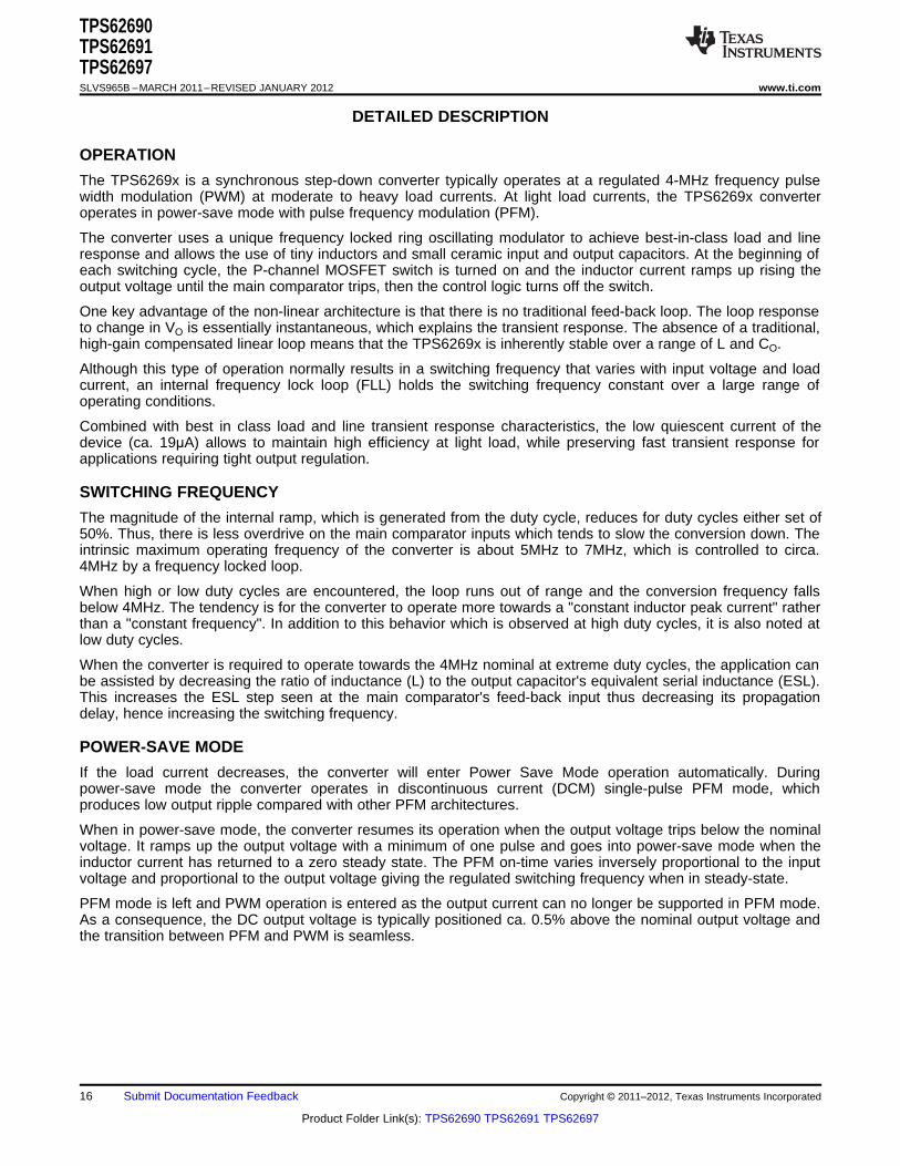
PFM Mode at Light Load
PFM Ripple
PWM Mode at Heavy LoadNominal DC Output Voltage
( )IN OUT OUT DS(on) LV min = V max + I max R max + R´
TPS62690TPS62691TPS62697
www.ti.com SLVS965B –MARCH 2011–REVISED JANUARY 2012
Figure 35. Operation in PFM Mode and Transfer to PWM Mode
MODE SELECTION
The MODE pin allows to select the operating mode of the device. Connecting this pin to GND enables theautomatic PWM and power-save mode operation. The converter operates in regulated frequency PWM mode atmoderate to heavy loads and in the PFM mode during light loads, which maintains high efficiency over a wideload current range.
Pulling the MODE pin high forces the converter to operate in the PWM mode even at light load currents. Theadvantage is that the converter modulates its switching frequency according to a spread spectrum PWMmodulation technique allowing simple filtering of the switching harmonics in noise-sensitive applications. In thismode, the efficiency is lower compared to the power-save mode during light loads.
For additional flexibility, it is possible to switch from power-save mode to PWM mode during operation. Thisallows efficient power management by adjusting the operation of the converter to the specific systemrequirements.
LOW DROPOUT, 100% DUTY CYCLE OPERATION
The device starts to enter 100% duty cycle mode once input and output voltage come close together. In order tomaintain the output voltage, the P-channel MOSFET is turned on 100% for one or more cycles.
With further decreasing VIN the high-side switch is constantly turned on, thereby providing a low input-to-outputvoltage difference. This is particularly useful in battery-powered applications to achieve longest operation time bytaking full advantage of the whole battery voltage range.
The minimum input voltage to maintain regulation depends on the load current and output voltage, and can becalculated as:
(1)
With:IOUTmax = Maximum output current, plus inductor ripple current.RDS(on)max = Maximum P-channel MOSFET RDS(on).RL = Inductor DC resistance.VOUTmax = Nominal output voltage, plus maximum output voltage tolerance.
Copyright © 2011–2012, Texas Instruments Incorporated Submit Documentation Feedback 17
Product Folder Link(s): TPS62690 TPS62691 TPS62697

TPS62690TPS62691TPS62697SLVS965B –MARCH 2011–REVISED JANUARY 2012 www.ti.com
ENABLE
The TPS6269x device starts operation when EN is set high and starts up with the soft start as previouslydescribed. For proper operation, the EN pin must be terminated and must not be left floating.
Pulling the EN pin low forces the device into shutdown, with a shutdown quiescent current of typically 0.2μA. Inthis mode, the P and N-channel MOSFETs are turned off, the internal resistor feedback divider is disconnected,and the entire internal-control circuitry is switched off.
The TPS6269x device can actively discharge the output capacitor when it turns off. The integrated dischargeresistor has a typical resistance of 100 Ω. The required time to discharge the output capacitor at the output nodedepends on load current and the output capacitance value.
SOFT START
The TPS6269x has an internal soft-start circuit that limits the inrush current during start-up. This limits inputvoltage drops when a battery or a high-impedance power source is connected to the input of the converter.
The soft-start system progressively increases the on-time from a minimum pulse-width of 35ns as a function ofthe output voltage. This mode of operation continues for c.a. 150μs after enable. Should the output voltage nothave reached its target value by this time, such as a heavy load, the soft-start transitions to a second mode ofoperation.
The converter then operates in a current limit mode, specifically the P-MOS current limit is set to half the nominallimit, and the N-channel MOSFET remains on until the inductor current has reset. After a further 150 μs, thedevice ramps up to the full current limit operation if the output voltage has risen above 0.5V (approximately).Therefore, the start-up time mainly depends on the output capacitor and load current.
UNDERVOLTAGE LOCKOUT
The undervoltage lockout circuit prevents the device from misoperation at low input voltages. It prevents theconverter from turning on the switch or rectifier MOSFET under undefined conditions. The TPS6269x devicehave a UVLO threshold set to 2.05V (typical). Fully functional operation is permitted down to 2.1V input voltage.
SHORT-CIRCUIT PROTECTION
The TPS6269x integrates a P-channel MOSFET current limit to protect the device against heavy load or shortcircuits. When the current in the P-channel MOSFET reaches its current limit, the P-channel MOSFET is turnedoff and the N-channel MOSFET is turned on. The regulator continues to limit the current on a cycle-by-cyclebasis.
As soon as the output voltage falls below ca. 0.4V, the converter current limit is reduced to half of the nominalvalue. Because the short-circuit protection is enabled during start-up, the device does not deliver more than halfof its nominal current limit until the output voltage exceeds approximately 0.5V. This needs to be consideredwhen a load acting as a current sink is connected to the output of the converter.
THERMAL SHUTDOWN
As soon as the junction temperature, TJ, exceeds typically 140°C, the device goes into thermal shutdown. In thismode, the P- and N-channel MOSFETs are turned off. The device continues its operation when the junctiontemperature again falls below typically 130°C.
18 Submit Documentation Feedback Copyright © 2011–2012, Texas Instruments Incorporated
Product Folder Link(s): TPS62690 TPS62691 TPS62697
IL
VOVI
VI VOL ƒsw
IL(MAX) IO(MAX) IL2
TPS62690TPS62691TPS62697
www.ti.com SLVS965B –MARCH 2011–REVISED JANUARY 2012
APPLICATION INFORMATION
INDUCTOR SELECTION
The TPS6269x series of step-down converters have been optimized to operate with an effective inductancevalue in the range of 0.5μH to 1.8μH and with output capacitors in the range of 4.7μF to 10μF. The internalcompensation is optimized to operate with an output filter of L = 1μH and CO = 4.7μF. Larger or smaller inductorvalues can be used to optimize the performance of the device for specific operation conditions. For more details,see the CHECKING LOOP STABILITY section.
The inductor value affects its peak-to-peak ripple current, the PWM-to-PFM transition point, the output voltageripple and the efficiency. The selected inductor has to be rated for its dc resistance and saturation current. Theinductor ripple current (ΔIL) decreases with higher inductance and increases with higher VI or VO.
with: fSW = switching frequency (4 MHz typical)
L = inductor value
ΔIL = peak-to-peak inductor ripple current
IL(MAX) = maximum inductor current (2)
In high-frequency converter applications, the efficiency is essentially affected by the inductor AC resistance (i.e.quality factor) and to a smaller extent by the inductor DCR value. To achieve high efficiency operation, careshould be taken in selecting inductors featuring a quality factor above 25 at the switching frequency. Increasingthe inductor value produces lower RMS currents, but degrades transient response. For a given physical inductorsize, increased inductance usually results in an inductor with lower saturation current.
The total losses of the coil consist of both the losses in the DC resistance (DC)) and the followingfrequency-dependent components:• The losses in the core material (magnetic hysteresis loss, especially at high switching frequencies)• Additional losses in the conductor from the skin effect (current displacement at high frequencies)• Magnetic field losses of the neighboring windings (proximity effect)• Radiation losses
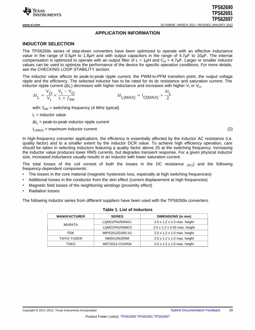
The following inductor series from different suppliers have been used with the TPS6269x converters.
Table 1. List of Inductors
MANUFACTURER SERIES DIMENSIONS (in mm)
LQM21PN1R0NGC 2.0 x 1.2 x 1.0 max. heightMURATA
LQM21PN1R5MC0 2.0 x 1.2 x 0.55 max. height
FDK MIPS2012D1R0-X2 2.0 x 1.2 x 1.0 max. height
TAIYO YUDEN NM2012N1R0M 2.0 x 1.2 x 1.0 max. height
TOKO MDT2012-CH1R0A 2.0 x 1.2 x 1.0 max. height
Copyright © 2011–2012, Texas Instruments Incorporated Submit Documentation Feedback 19
Product Folder Link(s): TPS62690 TPS62691 TPS62697

TPS62690TPS62691TPS62697SLVS965B –MARCH 2011–REVISED JANUARY 2012 www.ti.com
OUTPUT CAPACITOR SELECTION
The advanced fast-response voltage mode control scheme of the TPS6269x allows the use of tiny ceramiccapacitors. Ceramic capacitors with low ESR values have the lowest output voltage ripple and arerecommended. For best performance, the device should be operated with a minimum effective outputcapacitance of 1μF. The output capacitor requires either an X7R or X5R dielectric. Y5V and Z5U dielectriccapacitors, aside from their wide variation in capacitance over temperature, become resistive at high frequencies.
At nominal load current, the device operates in PWM mode and the overall output voltage ripple is the sum of thevoltage step caused by the output capacitor ESL and the ripple current flowing through the output capacitorimpedance.
At light loads, the output capacitor limits the output ripple voltage and provides holdup during large loadtransitions. A 4.7μF or 10μF ceramic capacitor typically provides sufficient bulk capacitance to stabilize the outputduring large load transitions. The typical output voltage ripple is ca. 0.5% to 1.5% of the nominal output voltageVO.
The output voltage ripple during PFM mode operation can be kept small. The PFM pulse is time controlled, whichallows to modify the charge transferred to the output capacitor by the value of the inductor. The resulting PFMoutput voltage ripple and PFM frequency depend in first order on the size of the output capacitor and the inductorvalue. The PFM frequency decreases with smaller inductor values and increases with larger once. Increasing theoutput capacitor value and the effective inductance will minimize the output ripple voltage.
INPUT CAPACITOR SELECTION
Because of the nature of the buck converter having a pulsating input current, a low ESR input capacitor isrequired to prevent large voltage transients that can cause misbehavior of the device or interferences with othercircuits in the system. For most applications, a 2.2 or 4.7-μF capacitor is sufficient. If the application exhibits anoisy or erratic switching frequency, the remedy should be found by experimenting with the value of the inputcapacitor.
Take care when using only ceramic input capacitors. When a ceramic capacitor is used at the input and thepower is being supplied through long wires, such as from a wall adapter, a load step at the output can induceringing at the VIN pin. This ringing can couple to the output and be mistaken as loop instability or could evendamage the part. Additional "bulk" capacitance (electrolytic or tantalum) should in this circumstance be placedbetween CI and the power source lead to reduce ringing than can occur between the inductance of the powersource leads and CI.
CHECKING LOOP STABILITY
The first step of circuit and stability evaluation is to look from a steady-state perspective at the following signals:• Switching node, SW• Inductor current, IL• Output ripple voltage, VO(AC)
These are the basic signals that need to be measured when evaluating a switching converter. When theswitching waveform shows large duty cycle jitter or the output voltage or inductor current shows oscillations, theregulation loop may be unstable. This is often a result of board layout and/or L-C combination.
As a next step in the evaluation of the regulation loop, the load transient response is tested. The time betweenthe application of the load transient and the turn on of the P-channel MOSFET, the output capacitor must supplyall of the current required by the load. VO immediately shifts by an amount equal to ΔI(LOAD) x ESR, where ESRis the effective series resistance of CO. ΔI(LOAD) begins to charge or discharge CO generating a feedback errorsignal used by the regulator to return VO to its steady-state value. The results are most easily interpreted whenthe device operates in PWM mode.
During this recovery time, VO can be monitored for settling time, overshoot or ringing that helps judge theconverter’s stability. Without any ringing, the loop has usually more than 45° of phase margin.
Because the damping factor of the circuitry is directly related to several resistive parameters (e.g., MOSFETrDS(on)) that are temperature dependant, the loop stability analysis has to be done over the input voltage range,load current range, and temperature range.
20 Submit Documentation Feedback Copyright © 2011–2012, Texas Instruments Incorporated
Product Folder Link(s): TPS62690 TPS62691 TPS62697
MODE
ENABLE
CIL
VIN
CO
VOUT
GND
J(MAX) AD(MAX)
JA
T - T 105 C - 85 CP = = = 160mW
R 125 C/Wq
° °
°
TPS62690TPS62691TPS62697
www.ti.com SLVS965B –MARCH 2011–REVISED JANUARY 2012
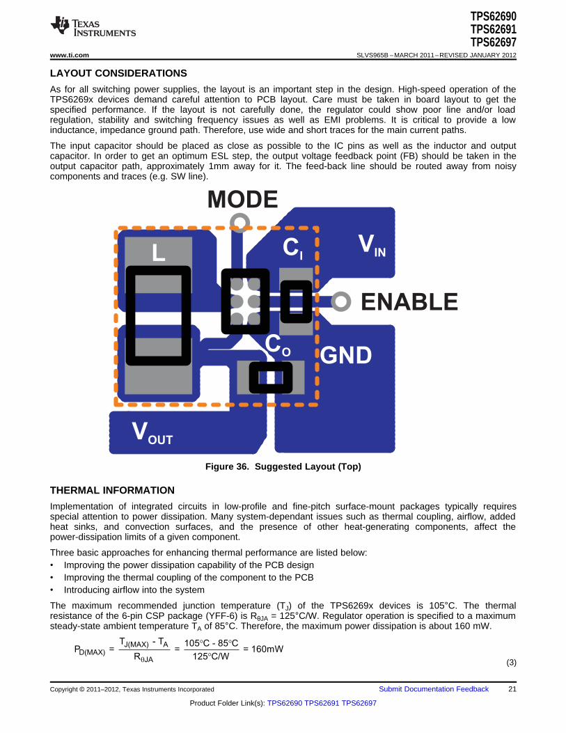
LAYOUT CONSIDERATIONS
As for all switching power supplies, the layout is an important step in the design. High-speed operation of theTPS6269x devices demand careful attention to PCB layout. Care must be taken in board layout to get thespecified performance. If the layout is not carefully done, the regulator could show poor line and/or loadregulation, stability and switching frequency issues as well as EMI problems. It is critical to provide a lowinductance, impedance ground path. Therefore, use wide and short traces for the main current paths.
The input capacitor should be placed as close as possible to the IC pins as well as the inductor and outputcapacitor. In order to get an optimum ESL step, the output voltage feedback point (FB) should be taken in theoutput capacitor path, approximately 1mm away for it. The feed-back line should be routed away from noisycomponents and traces (e.g. SW line).
Figure 36. Suggested Layout (Top)
THERMAL INFORMATION
Implementation of integrated circuits in low-profile and fine-pitch surface-mount packages typically requiresspecial attention to power dissipation. Many system-dependant issues such as thermal coupling, airflow, addedheat sinks, and convection surfaces, and the presence of other heat-generating components, affect thepower-dissipation limits of a given component.
Three basic approaches for enhancing thermal performance are listed below:• Improving the power dissipation capability of the PCB design• Improving the thermal coupling of the component to the PCB• Introducing airflow into the system
The maximum recommended junction temperature (TJ) of the TPS6269x devices is 105°C. The thermalresistance of the 6-pin CSP package (YFF-6) is RθJA = 125°C/W. Regulator operation is specified to a maximumsteady-state ambient temperature TA of 85°C. Therefore, the maximum power dissipation is about 160 mW.
(3)
Copyright © 2011–2012, Texas Instruments Incorporated Submit Documentation Feedback 21
Product Folder Link(s): TPS62690 TPS62691 TPS62697
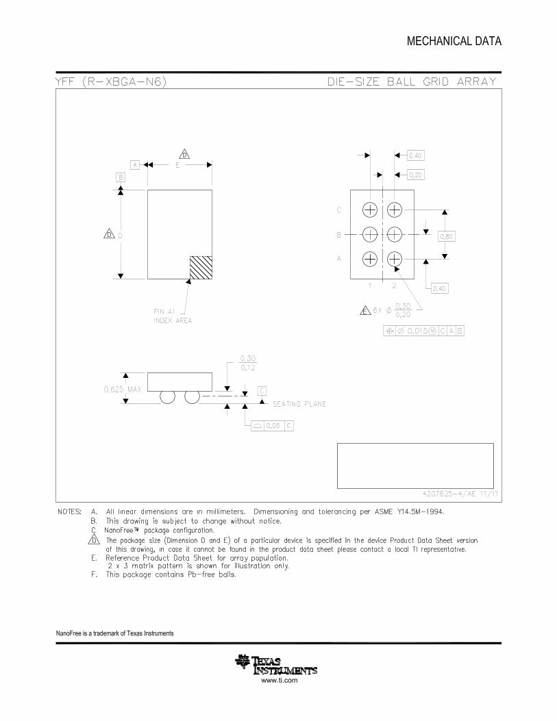
YMDS
CC
A1
A1
B1
C1
A2
B2D
E
C2
TPS62690TPS62691TPS62697SLVS965B –MARCH 2011–REVISED JANUARY 2012 www.ti.com
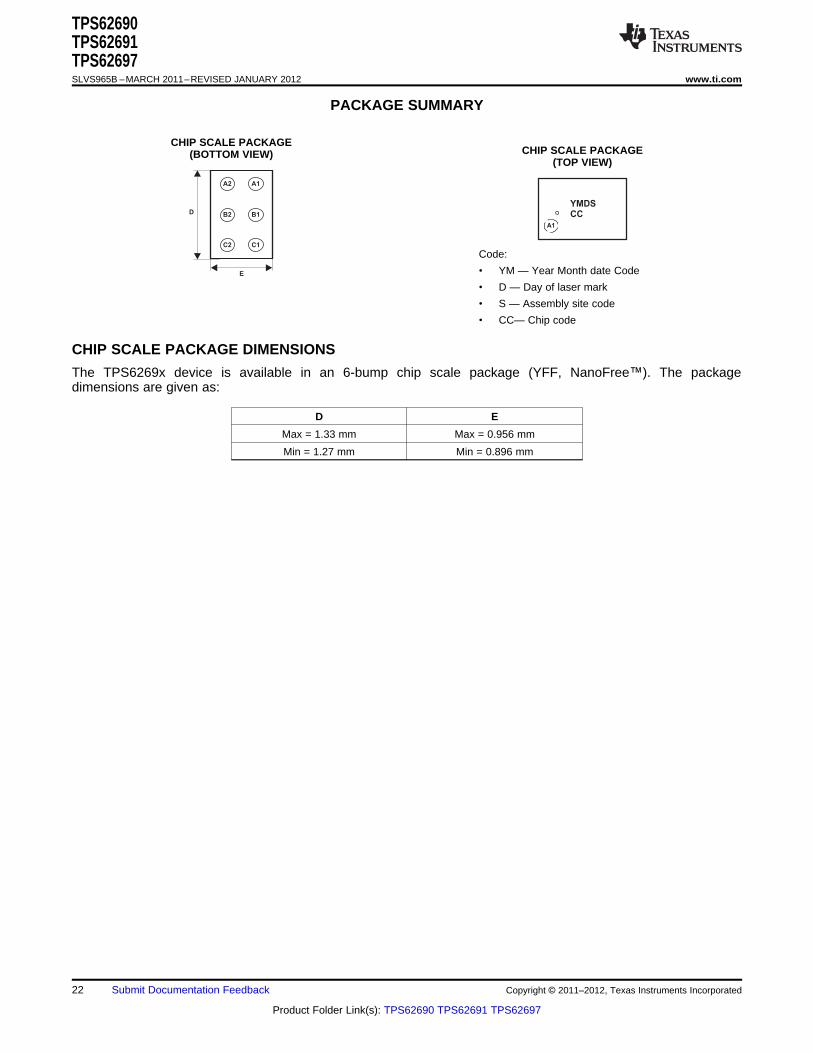
PACKAGE SUMMARY
CHIP SCALE PACKAGECHIP SCALE PACKAGE(BOTTOM VIEW)
(TOP VIEW)
Code:
• YM — Year Month date Code
• D — Day of laser mark
• S — Assembly site code
• CC— Chip code
CHIP SCALE PACKAGE DIMENSIONS
The TPS6269x device is available in an 6-bump chip scale package (YFF, NanoFree™). The packagedimensions are given as:
D E
Max = 1.33 mm Max = 0.956 mm
Min = 1.27 mm Min = 0.896 mm
22 Submit Documentation Feedback Copyright © 2011–2012, Texas Instruments Incorporated
Product Folder Link(s): TPS62690 TPS62691 TPS62697
a0182291
Typewritten Text
D: Max = 1.35 mm, Min = 1.25 mm
a0182291
Typewritten Text
a0182291
Typewritten Text
E: Max = 0.976 mm, Min = 0.876 mm
PACKAGE OPTION ADDENDUM
www.ti.com 15-Apr-2017
Addendum-Page 1
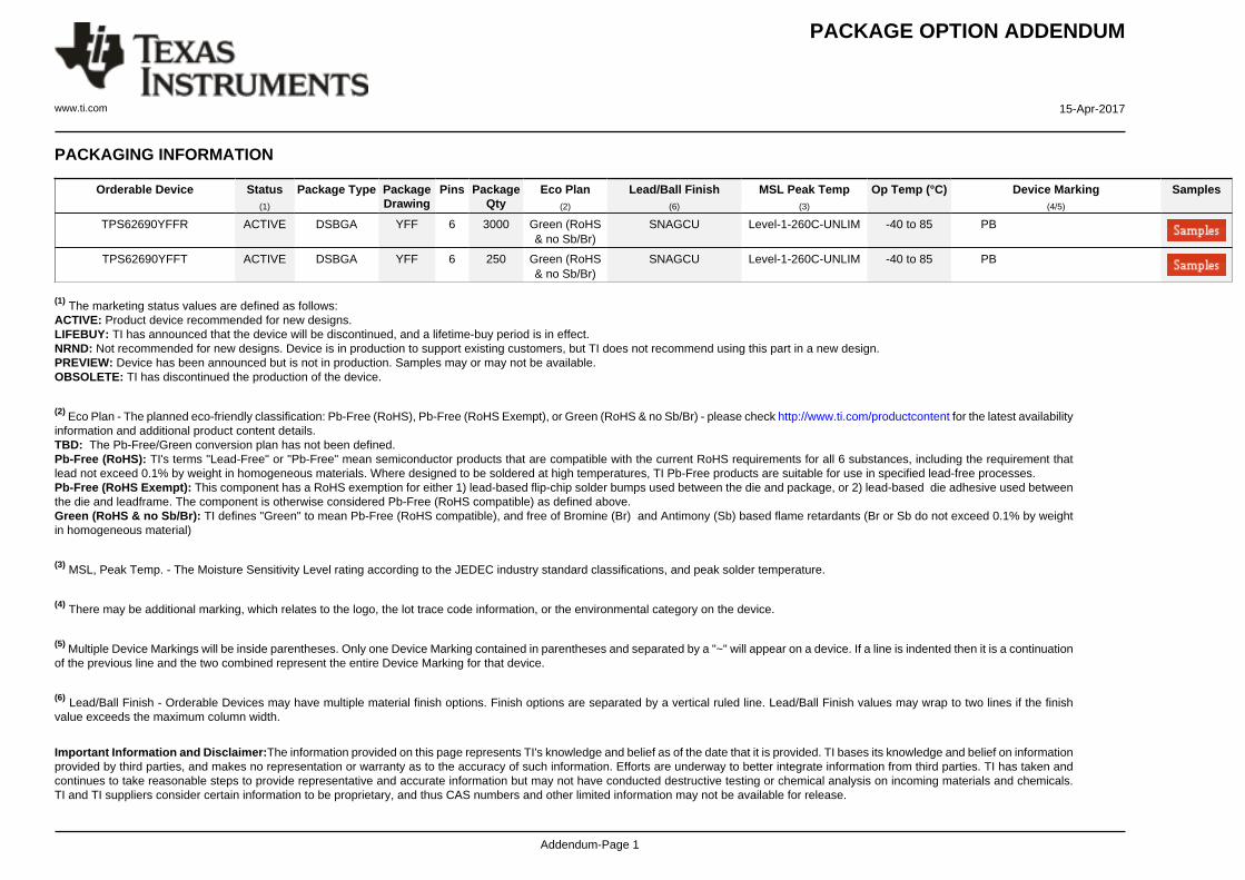
PACKAGING INFORMATION
Orderable Device Status(1)
Package Type PackageDrawing
Pins PackageQty
Eco Plan(2)
Lead/Ball Finish(6)
MSL Peak Temp(3)
Op Temp (°C) Device Marking(4/5)
Samples
TPS62690YFFR ACTIVE DSBGA YFF 6 3000 Green (RoHS& no Sb/Br)
SNAGCU Level-1-260C-UNLIM -40 to 85 PB
TPS62690YFFT ACTIVE DSBGA YFF 6 250 Green (RoHS& no Sb/Br)
SNAGCU Level-1-260C-UNLIM -40 to 85 PB
(1) The marketing status values are defined as follows:ACTIVE: Product device recommended for new designs.LIFEBUY: TI has announced that the device will be discontinued, and a lifetime-buy period is in effect.NRND: Not recommended for new designs. Device is in production to support existing customers, but TI does not recommend using this part in a new design.PREVIEW: Device has been announced but is not in production. Samples may or may not be available.OBSOLETE: TI has discontinued the production of the device.
(2) Eco Plan - The planned eco-friendly classification: Pb-Free (RoHS), Pb-Free (RoHS Exempt), or Green (RoHS & no Sb/Br) - please check http://www.ti.com/productcontent for the latest availabilityinformation and additional product content details.TBD: The Pb-Free/Green conversion plan has not been defined.Pb-Free (RoHS): TI's terms "Lead-Free" or "Pb-Free" mean semiconductor products that are compatible with the current RoHS requirements for all 6 substances, including the requirement thatlead not exceed 0.1% by weight in homogeneous materials. Where designed to be soldered at high temperatures, TI Pb-Free products are suitable for use in specified lead-free processes.Pb-Free (RoHS Exempt): This component has a RoHS exemption for either 1) lead-based flip-chip solder bumps used between the die and package, or 2) lead-based die adhesive used betweenthe die and leadframe. The component is otherwise considered Pb-Free (RoHS compatible) as defined above.Green (RoHS & no Sb/Br): TI defines "Green" to mean Pb-Free (RoHS compatible), and free of Bromine (Br) and Antimony (Sb) based flame retardants (Br or Sb do not exceed 0.1% by weightin homogeneous material)
(3) MSL, Peak Temp. - The Moisture Sensitivity Level rating according to the JEDEC industry standard classifications, and peak solder temperature.
(4) There may be additional marking, which relates to the logo, the lot trace code information, or the environmental category on the device.
(5) Multiple Device Markings will be inside parentheses. Only one Device Marking contained in parentheses and separated by a "~" will appear on a device. If a line is indented then it is a continuationof the previous line and the two combined represent the entire Device Marking for that device.
(6) Lead/Ball Finish - Orderable Devices may have multiple material finish options. Finish options are separated by a vertical ruled line. Lead/Ball Finish values may wrap to two lines if the finishvalue exceeds the maximum column width.
Important Information and Disclaimer:The information provided on this page represents TI's knowledge and belief as of the date that it is provided. TI bases its knowledge and belief on informationprovided by third parties, and makes no representation or warranty as to the accuracy of such information. Efforts are underway to better integrate information from third parties. TI has taken andcontinues to take reasonable steps to provide representative and accurate information but may not have conducted destructive testing or chemical analysis on incoming materials and chemicals.TI and TI suppliers consider certain information to be proprietary, and thus CAS numbers and other limited information may not be available for release.
PACKAGE OPTION ADDENDUM
www.ti.com 15-Apr-2017
Addendum-Page 2
In no event shall TI's liability arising out of such information exceed the total purchase price of the TI part(s) at issue in this document sold by TI to Customer on an annual basis.
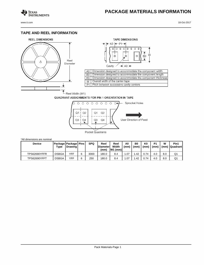
TAPE AND REEL INFORMATION
*All dimensions are nominal
Device PackageType
PackageDrawing
Pins SPQ ReelDiameter
(mm)
ReelWidth
W1 (mm)
A0(mm)
B0(mm)
K0(mm)
P1(mm)
W(mm)
Pin1Quadrant
TPS62690YFFR DSBGA YFF 6 3000 180.0 8.4 1.07 1.42 0.74 4.0 8.0 Q1
TPS62690YFFT DSBGA YFF 6 250 180.0 8.4 1.07 1.42 0.74 4.0 8.0 Q1
PACKAGE MATERIALS INFORMATION
www.ti.com 18-Oct-2017
Pack Materials-Page 1
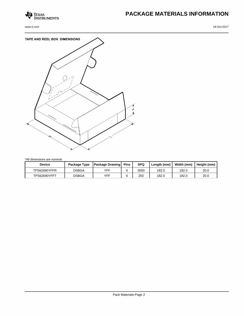
*All dimensions are nominal
Device Package Type Package Drawing Pins SPQ Length (mm) Width (mm) Height (mm)
TPS62690YFFR DSBGA YFF 6 3000 182.0 182.0 20.0
TPS62690YFFT DSBGA YFF 6 250 182.0 182.0 20.0
PACKAGE MATERIALS INFORMATION
www.ti.com 18-Oct-2017
Pack Materials-Page 2
IMPORTANT NOTICE
Texas Instruments Incorporated (TI) reserves the right to make corrections, enhancements, improvements and other changes to itssemiconductor products and services per JESD46, latest issue, and to discontinue any product or service per JESD48, latest issue. Buyersshould obtain the latest relevant information before placing orders and should verify that such information is current and complete.TI’s published terms of sale for semiconductor products (http://www.ti.com/sc/docs/stdterms.htm) apply to the sale of packaged integratedcircuit products that TI has qualified and released to market. Additional terms may apply to the use or sale of other types of TI products andservices.Reproduction of significant portions of TI information in TI data sheets is permissible only if reproduction is without alteration and isaccompanied by all associated warranties, conditions, limitations, and notices. TI is not responsible or liable for such reproduceddocumentation. Information of third parties may be subject to additional restrictions. Resale of TI products or services with statementsdifferent from or beyond the parameters stated by TI for that product or service voids all express and any implied warranties for theassociated TI product or service and is an unfair and deceptive business practice. TI is not responsible or liable for any such statements.Buyers and others who are developing systems that incorporate TI products (collectively, “Designers”) understand and agree that Designersremain responsible for using their independent analysis, evaluation and judgment in designing their applications and that Designers havefull and exclusive responsibility to assure the safety of Designers' applications and compliance of their applications (and of all TI productsused in or for Designers’ applications) with all applicable regulations, laws and other applicable requirements. Designer represents that, withrespect to their applications, Designer has all the necessary expertise to create and implement safeguards that (1) anticipate dangerousconsequences of failures, (2) monitor failures and their consequences, and (3) lessen the likelihood of failures that might cause harm andtake appropriate actions. Designer agrees that prior to using or distributing any applications that include TI products, Designer willthoroughly test such applications and the functionality of such TI products as used in such applications.TI’s provision of technical, application or other design advice, quality characterization, reliability data or other services or information,including, but not limited to, reference designs and materials relating to evaluation modules, (collectively, “TI Resources”) are intended toassist designers who are developing applications that incorporate TI products; by downloading, accessing or using TI Resources in anyway, Designer (individually or, if Designer is acting on behalf of a company, Designer’s company) agrees to use any particular TI Resourcesolely for this purpose and subject to the terms of this Notice.TI’s provision of TI Resources does not expand or otherwise alter TI’s applicable published warranties or warranty disclaimers for TIproducts, and no additional obligations or liabilities arise from TI providing such TI Resources. TI reserves the right to make corrections,enhancements, improvements and other changes to its TI Resources. TI has not conducted any testing other than that specificallydescribed in the published documentation for a particular TI Resource.Designer is authorized to use, copy and modify any individual TI Resource only in connection with the development of applications thatinclude the TI product(s) identified in such TI Resource. NO OTHER LICENSE, EXPRESS OR IMPLIED, BY ESTOPPEL OR OTHERWISETO ANY OTHER TI INTELLECTUAL PROPERTY RIGHT, AND NO LICENSE TO ANY TECHNOLOGY OR INTELLECTUAL PROPERTYRIGHT OF TI OR ANY THIRD PARTY IS GRANTED HEREIN, including but not limited to any patent right, copyright, mask work right, orother intellectual property right relating to any combination, machine, or process in which TI products or services are used. Informationregarding or referencing third-party products or services does not constitute a license to use such products or services, or a warranty orendorsement thereof. Use of TI Resources may require a license from a third party under the patents or other intellectual property of thethird party, or a license from TI under the patents or other intellectual property of TI.TI RESOURCES ARE PROVIDED “AS IS” AND WITH ALL FAULTS. TI DISCLAIMS ALL OTHER WARRANTIES ORREPRESENTATIONS, EXPRESS OR IMPLIED, REGARDING RESOURCES OR USE THEREOF, INCLUDING BUT NOT LIMITED TOACCURACY OR COMPLETENESS, TITLE, ANY EPIDEMIC FAILURE WARRANTY AND ANY IMPLIED WARRANTIES OFMERCHANTABILITY, FITNESS FOR A PARTICULAR PURPOSE, AND NON-INFRINGEMENT OF ANY THIRD PARTY INTELLECTUALPROPERTY RIGHTS. TI SHALL NOT BE LIABLE FOR AND SHALL NOT DEFEND OR INDEMNIFY DESIGNER AGAINST ANY CLAIM,INCLUDING BUT NOT LIMITED TO ANY INFRINGEMENT CLAIM THAT RELATES TO OR IS BASED ON ANY COMBINATION OFPRODUCTS EVEN IF DESCRIBED IN TI RESOURCES OR OTHERWISE. IN NO EVENT SHALL TI BE LIABLE FOR ANY ACTUAL,DIRECT, SPECIAL, COLLATERAL, INDIRECT, PUNITIVE, INCIDENTAL, CONSEQUENTIAL OR EXEMPLARY DAMAGES INCONNECTION WITH OR ARISING OUT OF TI RESOURCES OR USE THEREOF, AND REGARDLESS OF WHETHER TI HAS BEENADVISED OF THE POSSIBILITY OF SUCH DAMAGES.Unless TI has explicitly designated an individual product as meeting the requirements of a particular industry standard (e.g., ISO/TS 16949and ISO 26262), TI is not responsible for any failure to meet such industry standard requirements.Where TI specifically promotes products as facilitating functional safety or as compliant with industry functional safety standards, suchproducts are intended to help enable customers to design and create their own applications that meet applicable functional safety standardsand requirements. Using products in an application does not by itself establish any safety features in the application. Designers mustensure compliance with safety-related requirements and standards applicable to their applications. Designer may not use any TI products inlife-critical medical equipment unless authorized officers of the parties have executed a special contract specifically governing such use.Life-critical medical equipment is medical equipment where failure of such equipment would cause serious bodily injury or death (e.g., lifesupport, pacemakers, defibrillators, heart pumps, neurostimulators, and implantables). Such equipment includes, without limitation, allmedical devices identified by the U.S. Food and Drug Administration as Class III devices and equivalent classifications outside the U.S.TI may expressly designate certain products as completing a particular qualification (e.g., Q100, Military Grade, or Enhanced Product).Designers agree that it has the necessary expertise to select the product with the appropriate qualification designation for their applicationsand that proper product selection is at Designers’ own risk. Designers are solely responsible for compliance with all legal and regulatoryrequirements in connection with such selection.Designer will fully indemnify TI and its representatives against any damages, costs, losses, and/or liabilities arising out of Designer’s non-compliance with the terms and provisions of this Notice.
Mailing Address: Texas Instruments, Post Office Box 655303, Dallas, Texas 75265Copyright © 2017, Texas Instruments Incorporated