
USART-Universal Synchronous A Synchronous Receiver Transmitter
TPS51225, TPS51225B, TPS51225Cwww.ti.com SLUSAV0B –JANUARY 2012–REVISED SEPTEMBER 2012
Dual Synchronous, Step-Down Controller with 5-V and 3.3-V LDOsCheck for Samples: TPS51225, TPS51225B, TPS51225C
1FEATURES APPLICATIONS2• Input Voltage Range: 5.5 V to 24 V • Notebook Computers• Output Voltages: 5 V and 3.3 V (Adjustable • Netbook, Tablet Computers
Range ±10%)DESCRIPTION• Built-in, 100-mA, 5-V and 3.3-V LDOsThe TPS51225/B/C is a cost-effective, dual-• Clock Output for Charge-Pumpsynchronous buck controller targeted for notebook
• ±1% Reference Accuracy system-power supply solutions. It provides 5-V and• Adaptive On-time D-CAP™ Mode Control 3.3-V LDOs and requires few external components.
The 260-kHz VCLK output can be used to drive anArchitecture with 300kHz/355kHz Frequencyexternal charge pump, generating gate drive voltageSettingfor the load switches without reducing the main• Auto-skip Light Load Operation (TPS51225/C)converter efficiency. The TPS51225/B/C supports
• OOA Light Load Operation (TPS51225B) high efficiency, fast transient response and provides acombined power-good signal. Adaptive on-time, D-• Internal 0.8-ms Voltage Servo Soft-StartCAP™ control provides convenient and efficient• Low-Side RDS(on) Current Sensing Scheme withoperation. The device operates with supply input4500 ppm/°C Temperature Coefficientvoltage ranging from 5.5 V to 24 V and supports
• Built-in Output Discharge Function output voltages of 5.0 V and 3.3 V. TheTPS51225/B/C is available in a 20-pin, 3 mm × 3• Separate Enable Input for Switchersmm, QFN package and is specified from –40°C to(TPS51225/B/C)85°C.• Dedicated OC Setting Terminals
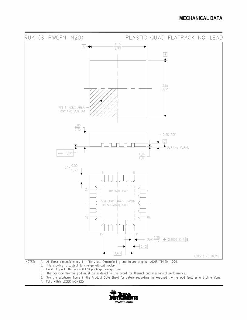
• Power Good Indicator• OVP/UVP/OCP Protection• Non-latch UVLO/OTP Protection• 20-Pin, 3 mm × 3 mm, QFN (RUK)
ORDERING INFORMATION (1)
ORDERABLE ENABLE OUTPUTSKIP MODE ALWAYS ON-LDO PACKAGE QUANTITYFUNCTION SUPPLYDEVICE NUMBER
TPS51225RUKR Tape and Reel 3000EN1/ EN2 Auto-skip VREG3
TPS51225RUKT Mini reel 250PLASTIC QuadTPS51225BRUKR Tape and Reel 3000
Flat PackEN1/ EN2 OOA VREG3TPS51225BRUKT Mini reel 250(20 pin QFN)TPS51225CRUKR Tape and Reel 3000
EN1/ EN2 Auto-skip VREG3 & VREG5TPS51225CRUKT Mini reel 250
(1) For the most current package and ordering information see the Package Option Addendum at the end of this document, or see the TIwebsite at www.ti.com.
1
Please be aware that an important notice concerning availability, standard warranty, and use in critical applications ofTexas Instruments semiconductor products and disclaimers thereto appears at the end of this data sheet.
2D-CAP, Out-of-Audio are trademarks of Texas Instruments.
PRODUCTION DATA information is current as of publication date. Copyright © 2012, Texas Instruments IncorporatedProducts conform to specifications per the terms of the TexasInstruments standard warranty. Production processing does notnecessarily include testing of all parameters.

VIN
VBST1
TPS51225C
DRVH1
SW1
DRVL1
VO1
VFB1
CS1
EN1EN 5 V
VCLK
VREG5
VIN
5.5 V to 24 V
VOUT
5 V
VOUT
15 V
VBST2
DRVH2
SW2
DRVL2
VFB2
CS2
EN2
PGOOD
VREG3
EN 3.3 V
VOUT
3.3 V
PGOOD
3.3-V Always ON
UDG-12001
1 mF1 mF
5 V
Always ON
VIN
VBST1
TPS51225
TPS51225 B
DRVH1
SW1
DRVL1
VO1
VFB1
CS1
EN1EN-5V
VCLK
VREG5
VIN
5.5 V to 24 V
VOUT
5 V
VOUT
15 V
VBST2
DRVH2
SW2
DRVL2
VFB2
CS2
EN2
PGOOD
VREG3
EN 3.3 V
VOUT
3.3 V
PGOOD
3.3-V Always ON
UDG-11182
1 mF
5 V
1 mF
TPS51225, TPS51225B, TPS51225CSLUSAV0B –JANUARY 2012–REVISED SEPTEMBER 2012 www.ti.com
These devices have limited built-in ESD protection. The leads should be shorted together or the device placed in conductive foamduring storage or handling to prevent electrostatic damage to the MOS gates.
TYPICAL APPLICATION DIAGRAM (TPS51225/TPS51225B)
TYPICAL APPLICATION DIAGRAM (TPS51225C)
2 Submit Documentation Feedback Copyright © 2012, Texas Instruments Incorporated
Product Folder Links :TPS51225 TPS51225B TPS51225C
TPS51225, TPS51225B, TPS51225Cwww.ti.com SLUSAV0B –JANUARY 2012–REVISED SEPTEMBER 2012
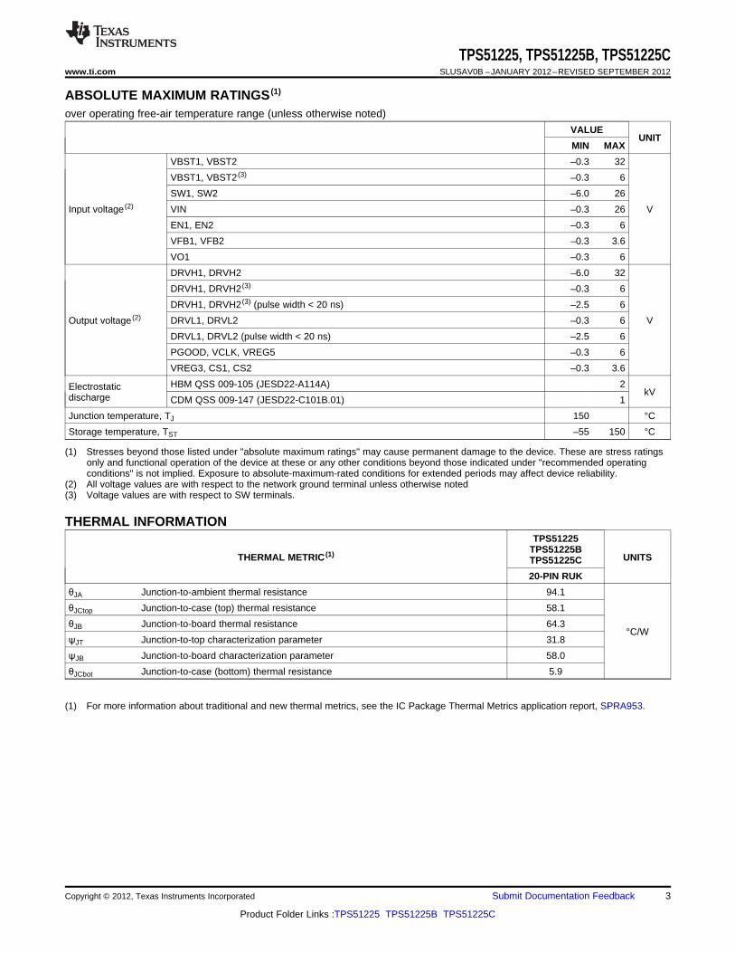
ABSOLUTE MAXIMUM RATINGS (1)
over operating free-air temperature range (unless otherwise noted)
VALUEUNIT
MIN MAX
VBST1, VBST2 –0.3 32
VBST1, VBST2 (3) –0.3 6
SW1, SW2 –6.0 26
Input voltage (2) VIN –0.3 26 V
EN1, EN2 –0.3 6
VFB1, VFB2 –0.3 3.6
VO1 –0.3 6
DRVH1, DRVH2 –6.0 32
DRVH1, DRVH2 (3) –0.3 6
DRVH1, DRVH2 (3) (pulse width < 20 ns) –2.5 6
Output voltage (2) DRVL1, DRVL2 –0.3 6 V
DRVL1, DRVL2 (pulse width < 20 ns) –2.5 6
PGOOD, VCLK, VREG5 –0.3 6
VREG3, CS1, CS2 –0.3 3.6
HBM QSS 009-105 (JESD22-A114A) 2Electrostatic kVdischarge CDM QSS 009-147 (JESD22-C101B.01) 1
Junction temperature, TJ 150 °C
Storage temperature, TST –55 150 °C
(1) Stresses beyond those listed under "absolute maximum ratings" may cause permanent damage to the device. These are stress ratingsonly and functional operation of the device at these or any other conditions beyond those indicated under "recommended operatingconditions" is not implied. Exposure to absolute-maximum-rated conditions for extended periods may affect device reliability.
(2) All voltage values are with respect to the network ground terminal unless otherwise noted(3) Voltage values are with respect to SW terminals.
THERMAL INFORMATIONTPS51225
TPS51225BTHERMAL METRIC (1) UNITSTPS51225C
20-PIN RUK
θJA Junction-to-ambient thermal resistance 94.1
θJCtop Junction-to-case (top) thermal resistance 58.1
θJB Junction-to-board thermal resistance 64.3°C/W
ψJT Junction-to-top characterization parameter 31.8
ψJB Junction-to-board characterization parameter 58.0
θJCbot Junction-to-case (bottom) thermal resistance 5.9
(1) For more information about traditional and new thermal metrics, see the IC Package Thermal Metrics application report, SPRA953.
Copyright © 2012, Texas Instruments Incorporated Submit Documentation Feedback 3
Product Folder Links :TPS51225 TPS51225B TPS51225C
TPS51225, TPS51225B, TPS51225CSLUSAV0B –JANUARY 2012–REVISED SEPTEMBER 2012 www.ti.com
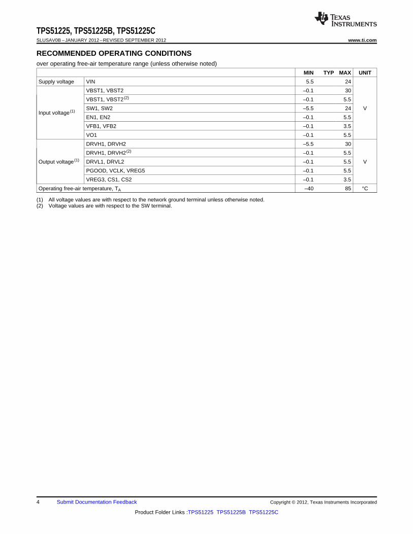
RECOMMENDED OPERATING CONDITIONSover operating free-air temperature range (unless otherwise noted)
MIN TYP MAX UNIT
Supply voltage VIN 5.5 24
VBST1, VBST2 –0.1 30
VBST1, VBST2 (2) –0.1 5.5
SW1, SW2 –5.5 24 VInput voltage (1)
EN1, EN2 –0.1 5.5
VFB1, VFB2 –0.1 3.5
VO1 –0.1 5.5
DRVH1, DRVH2 –5.5 30
DRVH1, DRVH2 (2) –0.1 5.5
Output voltage (1) DRVL1, DRVL2 –0.1 5.5 V
PGOOD, VCLK, VREG5 –0.1 5.5
VREG3, CS1, CS2 –0.1 3.5
Operating free-air temperature, TA –40 85 °C
(1) All voltage values are with respect to the network ground terminal unless otherwise noted.(2) Voltage values are with respect to the SW terminal.
4 Submit Documentation Feedback Copyright © 2012, Texas Instruments Incorporated
Product Folder Links :TPS51225 TPS51225B TPS51225C
TPS51225, TPS51225B, TPS51225Cwww.ti.com SLUSAV0B –JANUARY 2012–REVISED SEPTEMBER 2012
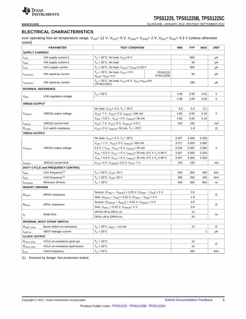
ELECTRICAL CHARACTERISTICSover operating free-air temperature range, VVIN= 12 V, VVO1= 5 V, VVFB1= VVFB2= 2 V, VEN1= VEN2= 3.3 V (unless otherwisenoted)
PARAMETER TEST CONDITION MIN TYP MAX UNIT
SUPPLY CURRENT
IVIN1 VIN supply current-1 TA = 25°C, No load, VVO1=0 V 860 μA
IVIN2 VIN supply current-2 TA = 25°C, No load 30 μA
IVO1 VO1 supply current TA = 25°C, No load, VVFB1= VVFB2=2.05 V 900 μA
TA = 25°C, No load, VVO1= 0 V, TPS51225IVIN(STBY) VIN stand-by current 95 μATPS51225BVEN1= VEN2= 0 V
TA = 25°C, No load, VVO1=0 V, VEN1=VEN2=0VIVIN(STBY) VIN stand-by current 180 μA(TPS51225C)
INTERNAL REFERENCE
TA = 25°C 1.99 2.00 2.01 VVFBx VFB regulation voltage
1.98 2.00 2.02 V
VREG5 OUTPUT
No load, VVO1= 0 V, TA = 25°C 4.9 5.0 5.1
VVREG5 VREG5 output voltage VVIN> 7 V , VVO1= 0 V, IVREG5< 100 mA 4.85 5.00 5.10 V
VVIN > 5.5 V , VVO1= 0 V, IVREG5< 35 mA 4.85 5.00 5.10
IVREG5 VREG5 current limit VVIN= 7 V, VVO1= 0 V, VVREG5= 4.5 V 100 150 mA
RV5SW 5-V switch resistance VVO1= 5 V, IVREG5= 50 mA, TA = 25°C 1.8 Ω
VREG3 OUTPUT
No load, VVO1= 0 V, TA = 25°C 3.267 3.300 3.333
VVIN > 7 V , VVO1= 0 V, IVREG3< 100 mA 3.217 3.300 3.383
VVREG3 VREG3 output voltage 5.5 V < VVIN , VVO1= 0 V, IVREG3< 35 mA 3.234 3.300 3.366 V
VVIN > 5.5 V, VVO1 = 0 V, IVREG3< 35 mA, 0°C ≤ TA ≤ 85°C 3.267 3.300 3.333
VVIN > 5.5 V, VVO1 = 5 V, IVREG3< 35 mA, 0°C ≤ TA ≤ 85°C 3.267 3.300 3.333
IVREG3 VREG3 current limit VVO1= 0 V, VVREG3= 3.0 V, VVIN= 7 V 100 150 mA
DUTY CYCLE and FREQUENCY CONTROL
fSW1 CH1 frequency (1) TA = 25°C, VVIN= 20 V 240 300 360 kHz
fSW2 CH2 frequency (1) TA = 25°C, VVIN= 20 V 280 355 430 kHz
tOFF(MIN) Minimum off-time TA = 25°C 200 300 500 ns
MOSFET DRIVERS
Source, (VVBST – VDRVH) = 0.25 V, (VVBST – VSW) = 5 V 3.0RDRVH DRVH resistance Ω
Sink, (VDRVH – VSW) = 0.25 V, (VVBST – VSW) = 5 V 1.9
Source, (VVREG5 – VDRVL) = 0.25 V, VVREG5 = 5 V 3.0RDRVL DRVL resistance Ω
Sink, VDRVL = 0.25 V, VVREG5= 5 V 0.9
DRVH-off to DRVL-on 12tD Dead time ns
DRVL-off to DRVH-on 20
INTERNAL BOOT STRAP SWITCH
RVBST (ON) Boost switch on-resistance TA = 25°C, IVBST = 10 mA 13 Ω
IVBSTLK VBST leakage current TA = 25°C 1 µA
CLOCK OUTPUT
RVCLK (PU) VCLK on-resistance (pull-up) TA = 25°C 10Ω
RVCLK (PD) VCLK on-resistance (pull-down) TA = 25°C 10
fCLK Clock frequency TA = 25°C 260 kHz
(1) Ensured by design. Not production tested.
Copyright © 2012, Texas Instruments Incorporated Submit Documentation Feedback 5
Product Folder Links :TPS51225 TPS51225B TPS51225C
TPS51225, TPS51225B, TPS51225CSLUSAV0B –JANUARY 2012–REVISED SEPTEMBER 2012 www.ti.com
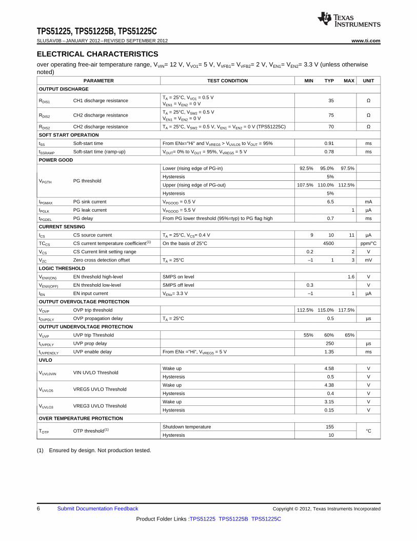
ELECTRICAL CHARACTERISTICSover operating free-air temperature range, VVIN= 12 V, VVO1= 5 V, VVFB1= VVFB2= 2 V, VEN1= VEN2= 3.3 V (unless otherwisenoted)
PARAMETER TEST CONDITION MIN TYP MAX UNIT
OUTPUT DISCHARGE
TA = 25°C, VVO1 = 0.5 VRDIS1 CH1 discharge resistance 35 Ω
VEN1 = VEN2 = 0 V
TA = 25°C, VSW2 = 0.5 VRDIS2 CH2 discharge resistance 75 Ω
VEN1 = VEN2 = 0 V
RDIS2 CH2 discharge resistance TA = 25°C, VSW2 = 0.5 V, VEN1 = VEN2 = 0 V (TPS51225C) 70 Ω
SOFT START OPERATION
tSS Soft-start time From ENx="Hi" and VVREG5 > VUVLO5 to VOUT = 95% 0.91 ms
tSSRAMP Soft-start time (ramp-up) VOUT= 0% to VOUT = 95%, VVREG5 = 5 V 0.78 ms
POWER GOOD
Lower (rising edge of PG-in) 92.5% 95.0% 97.5%
Hysteresis 5%VPGTH PG threshold
Upper (rising edge of PG-out) 107.5% 110.0% 112.5%
Hysteresis 5%
IPGMAX PG sink current VPGOOD = 0.5 V 6.5 mA
IPGLK PG leak current VPGOOD = 5.5 V 1 µA
tPGDEL PG delay From PG lower threshold (95%=typ) to PG flag high 0.7 ms
CURRENT SENSING
ICS CS source current TA = 25°C, VCS= 0.4 V 9 10 11 μA
TCCS CS current temperature coefficient (1) On the basis of 25°C 4500 ppm/°C
VCS CS Current limit setting range 0.2 2 V
VZC Zero cross detection offset TA = 25°C –1 1 3 mV
LOGIC THRESHOLD
VENX(ON) EN threshold high-level SMPS on level 1.6 V
VENX(OFF) EN threshold low-level SMPS off level 0.3 V
IEN EN input current VENx= 3.3 V –1 1 µA
OUTPUT OVERVOLTAGE PROTECTION
VOVP OVP trip threshold 112.5% 115.0% 117.5%
tOVPDLY OVP propagation delay TA = 25°C 0.5 µs
OUTPUT UNDERVOLTAGE PROTECTION
VUVP UVP trip Threshold 55% 60% 65%
tUVPDLY UVP prop delay 250 µs
tUVPENDLY UVP enable delay From ENx ="Hi", VVREG5 = 5 V 1.35 ms
UVLO
Wake up 4.58 VVUVL0VIN VIN UVLO Threshold
Hysteresis 0.5 V
Wake up 4.38 VVUVLO5 VREG5 UVLO Threshold
Hysteresis 0.4 V
Wake up 3.15 VVUVLO3 VREG3 UVLO Threshold
Hysteresis 0.15 V
OVER TEMPERATURE PROTECTION
Shutdown temperature 155TOTP OTP threshold (1) °C
Hysteresis 10
(1) Ensured by design. Not production tested.
6 Submit Documentation Feedback Copyright © 2012, Texas Instruments Incorporated
Product Folder Links :TPS51225 TPS51225B TPS51225C

1
2
3
4
5
6 7 8 9 10
11
12
13
14
15
1617181920
TPS51225
Thermal Pad
TPS51225B
TPS51225C
CS1
VFB1
VREG3
VFB2
CS2E
N2
PG
OO
D
SW
2
VB
ST
2
DR
VH
2
DRVL2
VIN
VREG5
VO1
DRVL1
DR
VH
1
VB
ST
1
SW
1
VC
LK
EN
1
TPS51225, TPS51225B, TPS51225Cwww.ti.com SLUSAV0B –JANUARY 2012–REVISED SEPTEMBER 2012
DEVICE INFORMATION
RUK PACKAGE20 PINS
(TOP VIEW)
PIN FUNCTIONSPIN NO.
TPS51225NAME I/O DESCRIPTIONTPS51225BTPS51225C
CS1 1 O Sets the channel 1 OCL trip level.
CS2 5 O Sets the channel 2OCL trip level.
DRVH1 16 O High-side driver output
DRVH2 10 O High-side driver output
DRVL1 15 O Low-side driver output
DRVL2 11 O Low-side driver output
EN1 20 I Channel 1 enable.
EN2 6 I Channel 2 enable.
PGOOD 7 O Power good output flag. Open drain output. Pull up to external rail via a resistor
SW1 18 O Switch-node connection.
SW2 8 O Switch-node connection.
VBST1 17 I Supply input for high-side MOSFET (bootstrap terminal). Connect capacitor from this pin to SWterminal.VBST2 9 I
VCLK 19 O Clock output for charge pump.
VFB1 2 IVoltage feedback Input
VFB2 4 I
Power conversion voltage input. Apply the same voltage as drain voltage of high-side MOSFETs ofVIN 12 I channel 1 and channel 2.
VO1 14 I Output voltage input, 5-V input for switch-over.
VREG3 3 O 3.3-V LDO output.
VREG5 13 O 5-V LDO output.
Thermal — — GND terminal, solder to the ground planepad
Copyright © 2012, Texas Instruments Incorporated Submit Documentation Feedback 7
Product Folder Links :TPS51225 TPS51225B TPS51225C
VIN
VBST1
TPS51225
TPS51225B
TPS51225C
DRVH1
SW1
DRVL1
VO1
VFB1
CS1
EN1
VCLK
VREG5
VBST2
DRVH2
SW2
DRVL2
VFB2
CS2
EN2
PGOOD
VREG3
UDG-12002
+ +
+
+
+
155°C/145°C
+
4.5 V/4.0 V
VO_OK
EN
FAULT
REF
PGOOD
DCHG
VIN VDDVDRV
GNDPGND
Switcher
Controller
(CH1)
EN
FAULT
REF
PGOOD
DCHG
VINVDD VDRV
GND PGND
Switcher
Controller
(CH2)
+ 2 V
Osc
GND
(Thermal Pad)
TPS51225, TPS51225B, TPS51225CSLUSAV0B –JANUARY 2012–REVISED SEPTEMBER 2012 www.ti.com
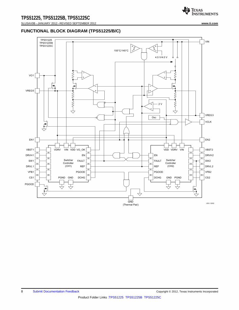
FUNCTIONAL BLOCK DIAGRAM (TPS51225/B/C)
8 Submit Documentation Feedback Copyright © 2012, Texas Instruments Incorporated
Product Folder Links :TPS51225 TPS51225B TPS51225C
DCHG
SW
TPS51225
TPS51225B
TPS51225C
NOC
ZC
XCON
VO_OK
DRVL
PWM
Control Logic
UDG-12007
+
+
VREF +15%
+
+
SKIP
UV
OV
VREF –40%
+
VIN
GND
REF
One-Shot
Discharge
10 µA
VBST
DRVH
FAULT
PGOOD
CS
+
VFB
OC+
+SS Ramp Comp
VREF +5%/10%
VREF –5%/10%
+
+
EN
VDD
HS
LS
VDRV
PGND
PGOOD
TPS51225, TPS51225B, TPS51225Cwww.ti.com SLUSAV0B –JANUARY 2012–REVISED SEPTEMBER 2012
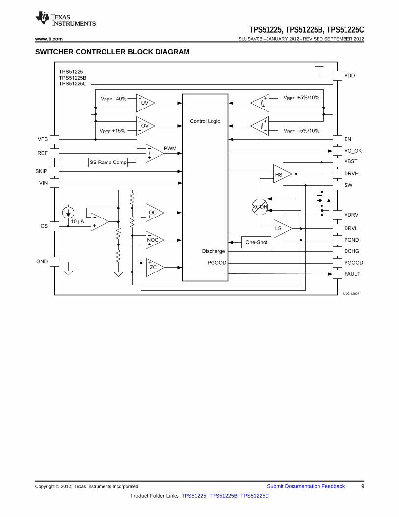
SWITCHER CONTROLLER BLOCK DIAGRAM
Copyright © 2012, Texas Instruments Incorporated Submit Documentation Feedback 9
Product Folder Links :TPS51225 TPS51225B TPS51225C
( )( )- ´
= ´´ ´
IN OUT OUT
OUT LLSW IN
V V V1I
2 L f V
TPS51225, TPS51225B, TPS51225CSLUSAV0B –JANUARY 2012–REVISED SEPTEMBER 2012 www.ti.com
DETAILED DESCRIPTION
PWM Operations
The main control loop of the switch mode power supply (SMPS) is designed as an adaptive on-time pulse widthmodulation (PWM) controller. It supports a proprietary D-CAP™ mode. D-CAP™ mode does not require externalconpensation circuit and is suitable for low external component count configuration when used with appropriateamount of ESR at the output capacitor(s).
At the beginning of each cycle, the synchronous high-side MOSFET is turned on, or enters the ON state. ThisMOSFET is turned off, or enters the ‘OFF state, after the internal, one-shot timer expires. The MOSFET is turnedon again when the feedback point voltage, VVFB, decreased to match the internal 2-V reference. The inductorcurrent information is also monitored and should be below the overcurrent threshold to initiate this new cycle. Byrepeating the operation in this manner, the controller regulates the output voltage. The synchronous low-side(rectifying) MOSFET is turned on at the beginning of each OFF state to maintain a minimum of conduction loss.The low-side MOSFET is turned off before the high-side MOSFET turns on at next switching cycle or wheninductor current information detects zero level. This enables seamless transition to the reduced frequencyoperation during light-load conditions so that high efficiency is maintained over a broad range of load current.
Adaptive On-Time/ PWM Frequency Control
Bacause the TPS51225/B/C does not have a dedicated oscillator for control loop on board, switching cycle iscontrolled by the adaptive on-time circuit. The on-time is controlled to meet the target switching frequency byfeed-forwarding the input and output voltage into the on-time one-shot timer. The target switching frequency isvaried according to the input voltage to achieve higher duty operation for lower input voltage application. Theswitching frequency of CH1 (5-V output) is 300 kHz during continuous conduction mode (CCM) operation whenVIN = 20 V. The CH2 (3.3-V output) is 355 kHz during CCM when VIN = 20 V.
Light Load Condition in Auto-Skip Operation (TPS51225/C)
The TPS51225/C automatically reduces switching frequency during light-load conditions to maintain highefficiency. This reduction of frequency is achieved smoothly and without an increase in output voltage ripple. Amore detailed description of this operation is as follows. As the output current decreases from heavy-loadcondition, the inductor current is also reduced and eventually approaches valley zero current, which is theboundary between continuous conduction mode and discontinuous conduction mode. The rectifying MOSFET isturned off when this zero inductor current is detected. As the load current further decreases, the converter runs indiscontinuous conduction mode and it takes longer and longer to discharge the output capacitor to the level thatrequires the next ON cycle. The ON time is maintained the same as that in the heavy-load condition. In reverse,when the output current increase from light load to heavy load, the switching frequency increases to the presetvalue as the inductor current reaches to the continuous conduction. The transition load point to the light loadoperation IOUT(LL) (i.e. the threshold between continuous and discontinuous conduction mode) can be calculatedas shown in Equation 1.
where• fSW is the PWM switching frequency (1)
Switching frequency versus output current during light-load conditions is a function of inductance (L), inputvoltage (VIN) and output voltage (VOUT), but it decreases almost proportional to the output current from theIOUT(LL).
10 Submit Documentation Feedback Copyright © 2012, Texas Instruments Incorporated
Product Folder Links :TPS51225 TPS51225B TPS51225C
= £
p ´ ´
SW0
OUT
f1f
2 ESR C 4
R1
R2
Voltage
Divider
+
VFB
+
VREF
PWM Control
Logic
and
Divider
L
ESR
COUT
VC
RLOAD
IINDIOUT
UDG-12010
IC
Switching Modulator
Output
Capacitor
VOUT
TPS51225
TPS51225B
TPS51225C
VIN
DRVH
DRVL
TPS51225, TPS51225B, TPS51225Cwww.ti.com SLUSAV0B –JANUARY 2012–REVISED SEPTEMBER 2012
Light-Load Condition in Out-of-Audio™ Operation (TPS51225B)
Out-of-Audio™ (OOA) light-load mode is a unique control feature that keeps the switching frequency aboveacoustic audible frequencies toward a virtual no-load condition. During Out-of-Audio™ operation, the OOAcontrol circuit monitors the states of both MOSFETs and forces them to transition into the ON state if both ofMOSFETs are off for more than 40 μs. When both high-side and low-side MOSFETs are off for 40 µs during alight-load condition, the operation mode is changed to FCCM. This mode change initiates the low-side MOSFETon and pulls down the output voltage. Then, the high-side MOSFET is turned on and stops switching again.
Table 1. SKIP Mode Operation (TPS51225/B/C)
SKIP MODE OPERATION
TPS51225 Auto-skip
TPS51225B OOA
TPS51225C Auto-skip
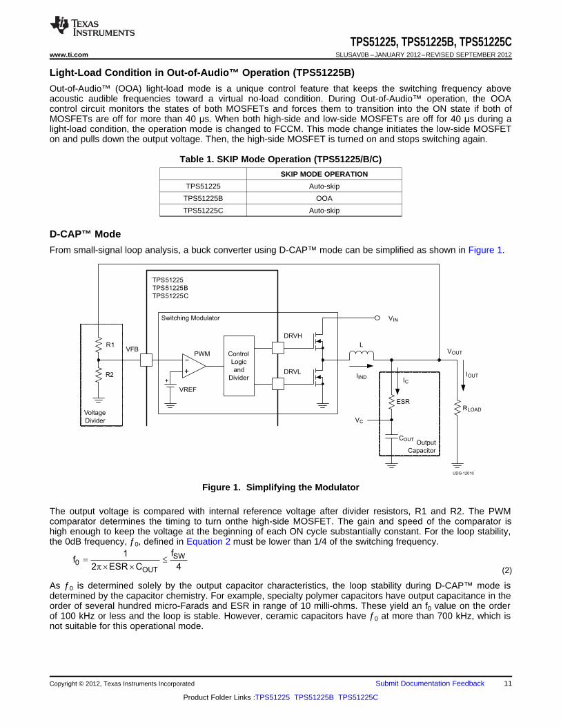
D-CAP™ Mode
From small-signal loop analysis, a buck converter using D-CAP™ mode can be simplified as shown in Figure 1.
Figure 1. Simplifying the Modulator
The output voltage is compared with internal reference voltage after divider resistors, R1 and R2. The PWMcomparator determines the timing to turn onthe high-side MOSFET. The gain and speed of the comparator ishigh enough to keep the voltage at the beginning of each ON cycle substantially constant. For the loop stability,the 0dB frequency, ƒ0, defined in Equation 2 must be lower than 1/4 of the switching frequency.
(2)
As ƒ0 is determined solely by the output capacitor characteristics, the loop stability during D-CAP™ mode isdetermined by the capacitor chemistry. For example, specialty polymer capacitors have output capacitance in theorder of several hundred micro-Farads and ESR in range of 10 milli-ohms. These yield an f0 value on the orderof 100 kHz or less and the loop is stable. However, ceramic capacitors have ƒ0 at more than 700 kHz, which isnot suitable for this operational mode.
Copyright © 2012, Texas Instruments Incorporated Submit Documentation Feedback 11
Product Folder Links :TPS51225 TPS51225B TPS51225C
VIN-UVLO_threshold
EN_threshold
95% of VOUT
95% of Vout
EN_threshold
VIN
VREG3
EN1
VREG5
5-V VOUT
PGOOD
EN2
Soft-Start Time (tSS)
Soft-Start Time
(tSS(ramp))
Soft-Start Time (tSS)
Soft-Start Time
(tSS(ramp))
PGOOD
Delay
tPGDEL
3.3-V VOUT
UDG-12013
VREG5-UVLO_threshold
TPS51225, TPS51225B, TPS51225CSLUSAV0B –JANUARY 2012–REVISED SEPTEMBER 2012 www.ti.com
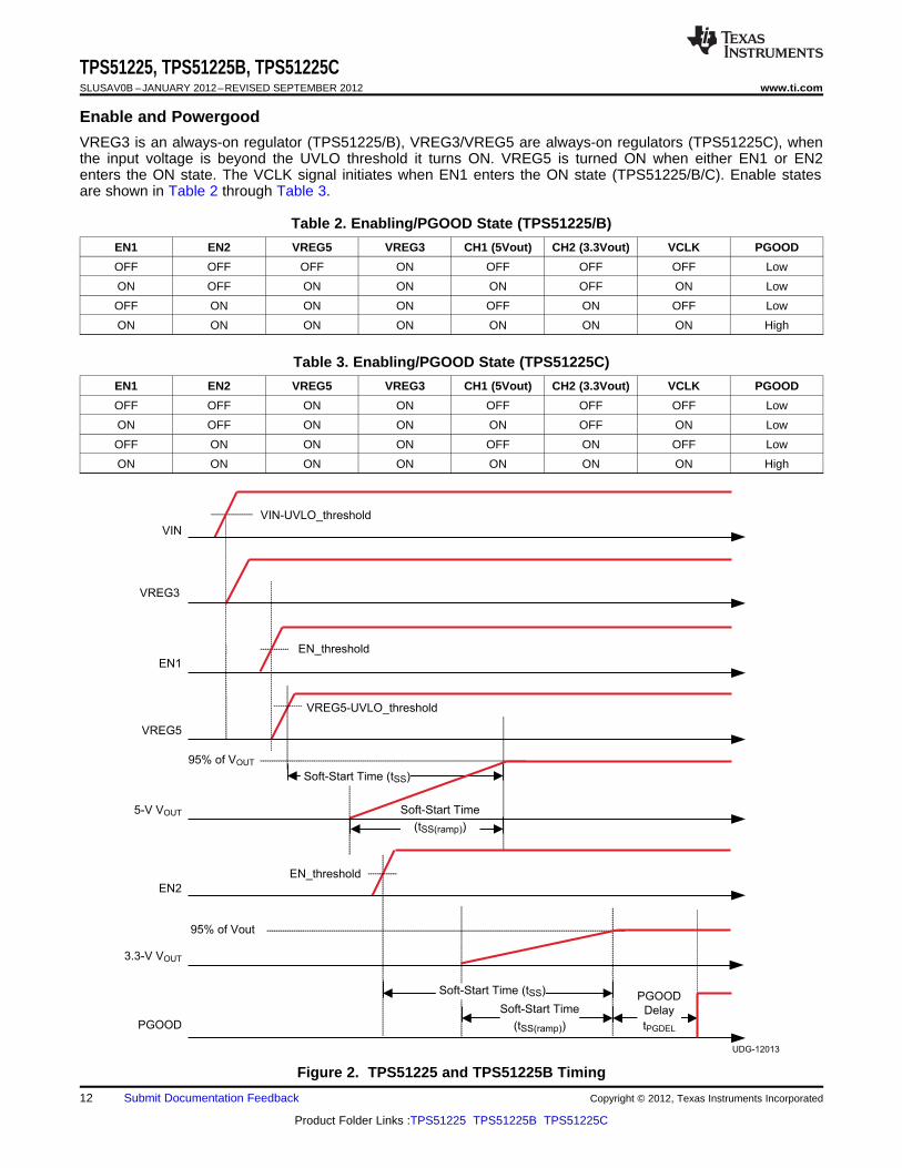
Enable and Powergood
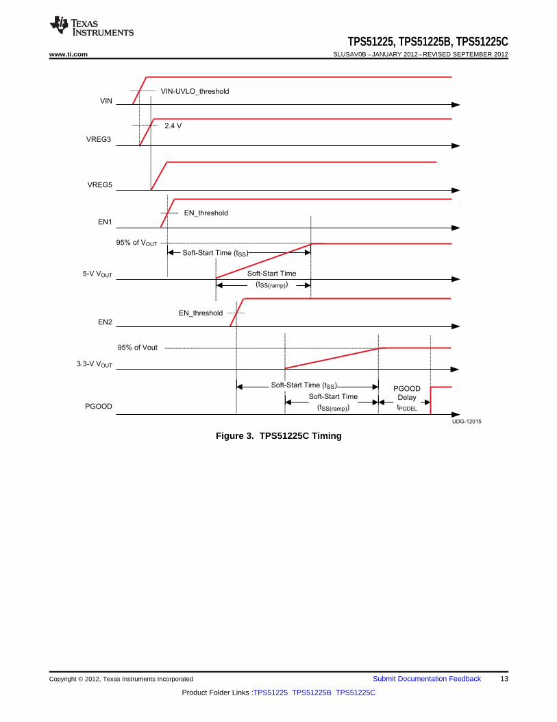
VREG3 is an always-on regulator (TPS51225/B), VREG3/VREG5 are always-on regulators (TPS51225C), whenthe input voltage is beyond the UVLO threshold it turns ON. VREG5 is turned ON when either EN1 or EN2enters the ON state. The VCLK signal initiates when EN1 enters the ON state (TPS51225/B/C). Enable statesare shown in Table 2 through Table 3.
Table 2. Enabling/PGOOD State (TPS51225/B)
EN1 EN2 VREG5 VREG3 CH1 (5Vout) CH2 (3.3Vout) VCLK PGOOD
OFF OFF OFF ON OFF OFF OFF Low
ON OFF ON ON ON OFF ON Low
OFF ON ON ON OFF ON OFF Low
ON ON ON ON ON ON ON High
Table 3. Enabling/PGOOD State (TPS51225C)
EN1 EN2 VREG5 VREG3 CH1 (5Vout) CH2 (3.3Vout) VCLK PGOOD
OFF OFF ON ON OFF OFF OFF Low
ON OFF ON ON ON OFF ON Low
OFF ON ON ON OFF ON OFF Low
ON ON ON ON ON ON ON High
Figure 2. TPS51225 and TPS51225B Timing
12 Submit Documentation Feedback Copyright © 2012, Texas Instruments Incorporated
Product Folder Links :TPS51225 TPS51225B TPS51225C
VIN-UVLO_threshold
95% of VOUT
95% of Vout
EN_threshold
VIN
VREG3
VREG5
5-V VOUT
PGOOD
EN2
Soft-Start Time (tSS)
Soft-Start Time
(tSS(ramp))
Soft-Start Time (tSS)
Soft-Start Time
(tSS(ramp))
PGOOD
Delay
tPGDEL
3.3-V VOUT
UDG-12015
EN_threshold
EN1
2.4 V
TPS51225, TPS51225B, TPS51225Cwww.ti.com SLUSAV0B –JANUARY 2012–REVISED SEPTEMBER 2012
Figure 3. TPS51225C Timing
Copyright © 2012, Texas Instruments Incorporated Submit Documentation Feedback 13
Product Folder Links :TPS51225 TPS51225B TPS51225C
( )
( )
( )
( )IND ripple IN OUT OUTTRIP TRIPOCP
SW INDS on DS on
I V V VV V 1I
R 2 R 2 L f V
- ´= + = + ´
´ ´
CS CSTRIP
R IV 1mV
8
´
= +
TPS51225, TPS51225B, TPS51225CSLUSAV0B –JANUARY 2012–REVISED SEPTEMBER 2012 www.ti.com
Soft-Start and Discharge
The TPS51225/B/C operates an internal, 0.8-ms, voltage servo soft-start for each channel. When the ENx pinbecomes higher than the enable threshold voltage, an internal DAC begins ramping up the reference voltage tothe PWM comparator. Smooth control of the output voltage is maintained during start-up. When ENx becomeslower than the lower level of threshold voltage, TPS51225/B/C discharges outputs using internal MOSFETsthrough VO1 (CH1) and SW2 (CH2).
VREG5/VREG3 Linear Regulators
There are two sets of 100-mA standby linear regulators which output 5 V and 3.3 V, respectively. The VREG5pin provides the current for the gate drivers. The VREG3 pin functions as the main power supply for the analogcircuitry of the device. VREG3 is an Always ON LDO and TPS51225C has Always ON VREG5. (see Table 2 andTable 3)
Add ceramic capacitors with a value of 1 µF or larger (X5R grade or better) placed close to the VREG5 andVREG3 pins to stabilize LDOs.
The VREG5 pin switchover function is asserted when three conditions are present:• CH1 internal PGOOD is high• CH1 is not in OCL condition• VO1 voltage is higher than VREG5-1V
In this switchover condition, three things occur:• the internal 5-V, LDO regulator is shut off• the VREG5 output is connected to VO1 by internal switchover MOSFET• VREG3 input pass is changed from VIN to VO1
VCLK for Charge Pump
The 260-kHz VCLK signal can be used in the charge pump circuit. The VCLK signal becomes available whenEN1. The VCLK driver is driven by VO1 voltage. In a design that does not require VCLK output, leave the VCLKpin open.
Overcurrent Protection
TPS51225/B/C has cycle-by-cycle over current limiting control. The inductor current is monitored during the OFFstate and the controller maintains the OFF state during the inductor current is larger than the overcurrent triplevel. In order to provide both good accuracy and cost effective solution, TPS51225/B/C supports temperaturecompensated MOSFET RDS(on) sensing. The CSx pin should be connected to GND through the CS voltagesetting resistor, RCS. The CSx pin sources CS current (ICS) which is 10 µA typically at room temperature, and theCSx terminal voltage (VCS= RCS × ICS) should be in the range of 0.2 V to 2 V over all operation temperatures. The trip level is set to the OCL trip voltage (VTRIP) as shown in Equation 3.
(3)
The inductor current is monitored by the voltage between GND pin and SWx pin so that SWx pin should beconnected to the drain terminal of the low-side MOSFET properly.The CS pin current has a 4500 ppm/°Ctemperature slope to compensate the temperature dependency of the RDS(on). GND is used as the positivecurrent sensing node so that GND should be connected to the source terminal of the low-side MOSFET.
As the comparison is done during the OFF state, VTRIP sets the valley level of the inductor current. Thus, the loadcurrent at the overcurrent threshold, IOCP, can be calculated as shown in Equation 4.
(4)
In an overcurrent condition, the current to the load exceeds the current to the output capacitor thus the outputvoltage tends to fall down. Eventually, it ends up with crossing the undervoltage protection threshold andshutdown both channels.
14 Submit Documentation Feedback Copyright © 2012, Texas Instruments Incorporated
Product Folder Links :TPS51225 TPS51225B TPS51225C
TPS51225, TPS51225B, TPS51225Cwww.ti.com SLUSAV0B –JANUARY 2012–REVISED SEPTEMBER 2012
Output Overvoltage/Undervoltage Protection
TPS51225/B/C asserts the overvoltage protection (OVP) when VFBx voltage reaches OVP trip threshold level.When an OVP event is detected, the controller changes the output target voltage to 0 V. This usually turns offDRVH and forces DRVL to be on. When the inductor current begins to flow through the low-side MOSFET andreaches the negative OCL, DRVL is turned off and DRVH is turned on. After the on-time expires, DRVH is turnedoff and DRVL is turned on again. This action minimizes the output node undershoot due to LC resonance. Whenthe VFBx reaches 0V, the driver output is latched as DRVH off, DRVL on. The undervoltage protection (UVP)latch is set when the VFBx voltage remains lower than UVP trip threshold voltage for 250 µs or longer. In thisfault condition, the controller latches DRVH low and DRVL low and discharges the outputs. UVP detectionfunction is enabled after 1.35 ms of SMPS operation to ensure startup.
Undervoltage Lockout (UVLO) Protection
TPS51225/B/C has undervoltage lock out protection at VIN, VREG5 and VREG3. When each voltage is lowerthan their UVLO threshold voltage, both SMPS are shut-off. They are non-latch protections.
Over-Temperature Protection
TPS51225/B/C features an internal temperature monitor. If the temperature exceeds the threshold value(typically 155°C), TPS51225/B/C is shut off including LDOs. This is non-latch protection.
Copyright © 2012, Texas Instruments Incorporated Submit Documentation Feedback 15
Product Folder Links :TPS51225 TPS51225B TPS51225C
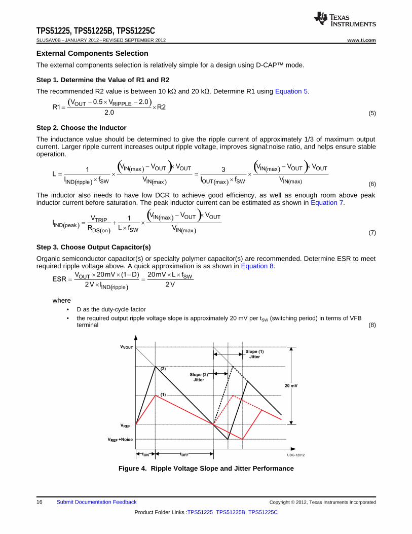
VVOUT
VREF
(2)
tON tOFF
Slope (2)
Jitter
20 mV
Slope (1)
Jitter
UDG-12012
VREF +Noise
(1)
( )
OUT SW
IND ripple
V 20mV (1 D) 20mV L fESR
2V I 2V
´ ´ - ´ ´= =
´
( )( )
( )( )( )
IN OUT OUTmaxTRIP
IND peakSW INDS on max
V V VV 1I
R L f V
- ´= + ´
´
( )
( )( )( ) ( )
( )( )- ´ - ´= ´ = ´
´ ´
IN OUT OUT IN OUT OUTmax max
SW IN OUT SW IN(max)IND ripple max max
V V V V V V1 3
LI f V I f V
( )OUT RIPPLEV 0.5 V 2.0R1 R2
2.0
- ´ -= ´
TPS51225, TPS51225B, TPS51225CSLUSAV0B –JANUARY 2012–REVISED SEPTEMBER 2012 www.ti.com
External Components Selection
The external components selection is relatively simple for a design using D-CAP™ mode.
Step 1. Determine the Value of R1 and R2
The recommended R2 value is between 10 kΩ and 20 kΩ. Determine R1 using Equation 5.
(5)
Step 2. Choose the Inductor
The inductance value should be determined to give the ripple current of approximately 1/3 of maximum outputcurrent. Larger ripple current increases output ripple voltage, improves signal:noise ratio, and helps ensure stableoperation.
(6)
The inductor also needs to have low DCR to achieve good efficiency, as well as enough room above peakinductor current before saturation. The peak inductor current can be estimated as shown in Equation 7.
(7)
Step 3. Choose Output Capacitor(s)
Organic semiconductor capacitor(s) or specialty polymer capacitor(s) are recommended. Determine ESR to meetrequired ripple voltage above. A quick approximation is as shown in Equation 8.
where• D as the duty-cycle factor• the required output ripple voltage slope is approximately 20 mV per tSW (switching period) in terms of VFB
terminal (8)
Figure 4. Ripple Voltage Slope and Jitter Performance
16 Submit Documentation Feedback Copyright © 2012, Texas Instruments Incorporated
Product Folder Links :TPS51225 TPS51225B TPS51225C
TPS51225, TPS51225B, TPS51225Cwww.ti.com SLUSAV0B –JANUARY 2012–REVISED SEPTEMBER 2012
Layout Considerations
Good layout is essential for stable power supply operation. Follow these guidelines for an efficient PCB layout.
Placement• Place voltage setting resistors close to the device pins.• Place bypass capacitors for VREG5 and VREG3 close to the device pins.
Routing (Sensitive analog portion)• Use small copper space for VFBx. There are short and narrow traces to avoid noise coupling.• Connect VFB resistor trace to the positive node of the output capacitor. Routing inner layer away from power
traces is recommended.• Use short and wide trace from VFB resistor to vias to GND (internal GND plane).
Routing (Power portion)• Use wider/shorter traces of DRVL for low-side gate drivers to reduce stray inductance.• Use the parallel traces of SW and DRVH for high-side MOSFET gate drive in a same layer or on adjoin
layers, and keep them away from DRVL.• Use wider/ shorter traces between the source terminal of the high-side MOSFET and the drain terminal of the
low-side MOSFET• Thermal pad is the GND terminal of this device. Five or more vias with 0.33-mm (13-mils) diameter connected
from the thermal pad to the internal GND plane should be used to have strong GND connection and help heatdissipation.
Copyright © 2012, Texas Instruments Incorporated Submit Documentation Feedback 17
Product Folder Links :TPS51225 TPS51225B TPS51225C
0
2
4
6
8
10
12
14
16
18
20
−40 −25 −10 5 20 35 50 65 80 95 110 125Junction Temperature (°C)
CS
Sou
rce
Cur
rent
(µA
)
G005
210
220
230
240
250
260
270
280
290
300
310
−40 −25 −10 5 20 35 50 65 80 95 110 125Junction Temperature (°C)
VC
LK F
requ
ency
(kH
z)
G006
0.0
0.2
0.4
0.6
0.8
1.0
1.2
1.4
1.6
−40 −25 −10 5 20 35 50 65 80 95 110 125Junction Temperature (°C)
VO
1 S
uppl
y C
urre
nt 1
(m
A)
G003
0
50
100
150
200
250
300
−40 −25 −10 5 20 35 50 65 80 95 110 125Junction Temperature (°C)
VIN
Sta
nd−
By
Cur
rent
(µA
)
TPS51225C Only
G004
0.0
0.2
0.4
0.6
0.8
1.0
1.2
1.4
1.6
−40 −25 −10 5 20 35 50 65 80 95 110 125Junction Temperature (°C)
VIN
Sup
ply
Cur
rent
1 (
mA
)
G001
0
10
20
30
40
50
60
−40 −25 −10 5 20 35 50 65 80 95 110 125Junction Temperature (°C)
VIN
Sup
ply
Cur
rent
2 (
µA)
G002
TPS51225, TPS51225B, TPS51225CSLUSAV0B –JANUARY 2012–REVISED SEPTEMBER 2012 www.ti.com
TYPICAL CHARACTERISTICS
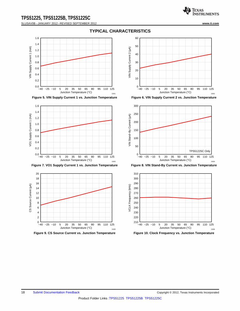
Figure 5. VIN Supply Current 1 vs. Junction Temperature Figure 6. VIN Supply Current 2 vs. Junction Temperature
Figure 7. VO1 Supply Current 1 vs. Junction Temperature Figure 8. VIN Stand-By Current vs. Junction Temperature
Figure 9. CS Source Current vs. Junction Temperature Figure 10. Clock Frequency vs. Junction Temperature
18 Submit Documentation Feedback Copyright © 2012, Texas Instruments Incorporated
Product Folder Links :TPS51225 TPS51225B TPS51225C
20
30
40
50
60
70
80
90
100
0.001 0.01 0.1 1 10Output Current (A)
Effi
cien
cy (
%)
VVIN = 8 VVVIN = 12 VVVIN = 20 V
Auto−SkipVVOUT = 3.3 V
G010
0
10
20
30
40
50
60
70
80
90
100
0.001 0.01 0.1 1 10Output Current (A)
Effi
cien
cy (
%)
VVIN = 8 VVVIN = 12 VVVIN = 20 V
Out−of_AudioVVOUT = 3.3 V
G011
4.85
4.90
4.95
5.00
5.05
5.10
5.15
0.001 0.01 0.1 1 10Output Current (A)
Out
put V
olag
e (V
)
VVIN = 8 VVVIN = 12 VVVIN = 20 V
Auto−SkipVVOUT = 5 V
G014
4.85
4.90
4.95
5.00
5.05
5.10
5.15
0.001 0.01 0.1 1 10Output Current (A)
Out
put V
olag
e (V
)
VVIN = 8 VVVIN = 12 VVVIN = 20 V
Out−of−AudioVVOUT = 5 V
G015
40
50
60
70
80
90
100
0.001 0.01 0.1 1 10Output Current (A)
Effi
cien
cy (
%)
VVIN = 8 VVVIN = 12 VVVIN = 20 V
Auto−SkipVVOUT = 5 V
G007
0
10
20
30
40
50
60
70
80
90
100
0.001 0.01 0.1 1 10Output Current (A)
Effi
cien
cy (
%)
VVIN = 8 VVVIN = 12 VVVIN = 20 V
Out−of−AudioVVOUT = 5 V
G008
TPS51225, TPS51225B, TPS51225Cwww.ti.com SLUSAV0B –JANUARY 2012–REVISED SEPTEMBER 2012
TYPICAL CHARACTERISTICS (continued)
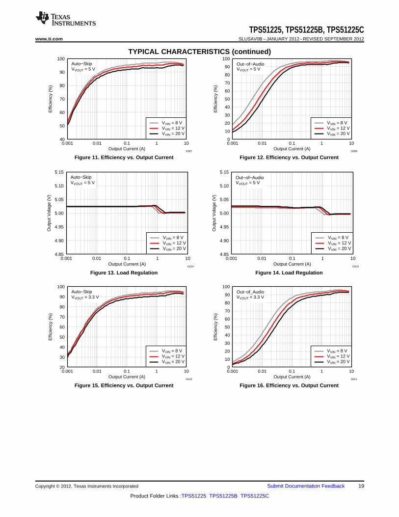
Figure 11. Efficiency vs. Output Current Figure 12. Efficiency vs. Output Current
Figure 13. Load Regulation Figure 14. Load Regulation
Figure 15. Efficiency vs. Output Current Figure 16. Efficiency vs. Output Current
Copyright © 2012, Texas Instruments Incorporated Submit Documentation Feedback 19
Product Folder Links :TPS51225 TPS51225B TPS51225C
0
50
100
150
200
250
300
350
400
450
0.001 0.01 0.1 1 10Output Current (A)
Sw
itchi
ng F
requ
ency
(kH
z)
VVIN = 8 VVVIN = 12 VVVIN = 20 V
Auto−SkipVVOUT = 3.3 V
G018
0
50
100
150
200
250
300
350
400
450
0.001 0.01 0.1 1 10Output Current (A)
Sw
itchi
ng F
requ
ency
(kH
z)
VVIN = 8 VVVIN = 12 VVVIN = 20 V
Out−of−AudioVVOUT = 3.3 V
G019
0
50
100
150
200
250
300
350
0.001 0.01 0.1 1 10Output Current (A)
Sw
itchi
ng F
requ
ency
(kH
z)
VVIN = 8 VVVIN = 12 VVVIN = 20 V
Auto−SkipVVOUT = 5 V
G016
0
50
100
150
200
250
300
350
0.001 0.01 0.1 1 10Output Current (A)
Sw
itchi
ng F
requ
ency
(kH
z)
VVIN = 8 VVVIN = 12 VVVIN = 20 V
Out−of−AudioVVOUT = 5 V
G017
3.23
3.28
3.33
3.38
3.43
0.001 0.01 0.1 1 10Output Current (A)
Out
put V
olag
e (V
)
VVIN = 8 VVVIN = 12 VVVIN = 20 V
Auto−skipVVOUT = 3.3 V
G012
3.23
3.28
3.33
3.38
3.43
0.001 0.01 0.1 1 10Output Current (A)
Out
put V
olag
e (V
)
VVIN = 8 VVVIN = 12 VVVIN = 20 V
Out−of−AudioVVOUT = 3.3 V
G013
TPS51225, TPS51225B, TPS51225CSLUSAV0B –JANUARY 2012–REVISED SEPTEMBER 2012 www.ti.com
TYPICAL CHARACTERISTICS (continued)
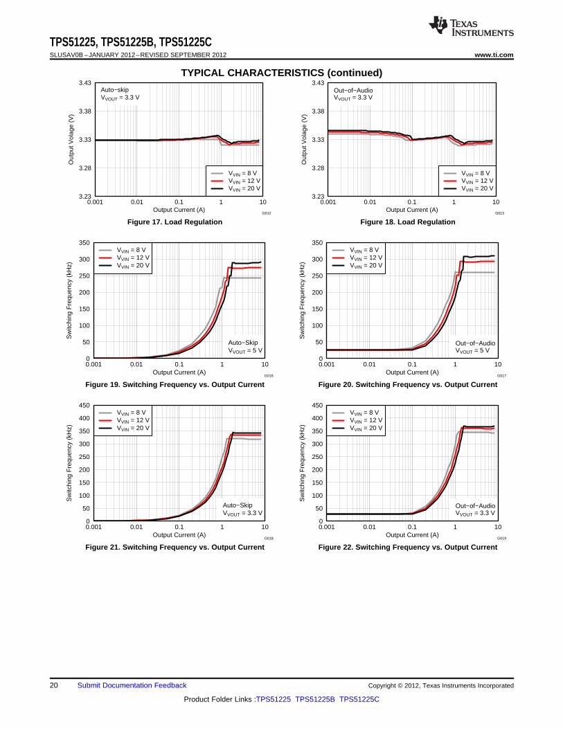
Figure 17. Load Regulation Figure 18. Load Regulation
Figure 19. Switching Frequency vs. Output Current Figure 20. Switching Frequency vs. Output Current
Figure 21. Switching Frequency vs. Output Current Figure 22. Switching Frequency vs. Output Current
20 Submit Documentation Feedback Copyright © 2012, Texas Instruments Incorporated
Product Folder Links :TPS51225 TPS51225B TPS51225C
0
50
100
150
200
250
300
350
400
450
500
5 10 15 20 25Input Voltage (V)
Sw
itchi
ng F
requ
ency
(kH
z)
VOUT = 5 VIOUT = 6 A
G000
0
50
100
150
200
250
300
350
400
450
500
5 10 15 20 25Input Voltage (V)
Sw
itchi
ng F
requ
ency
(kH
z)
VOUT = 3.3 VIOUT = 6 A
G000
Time (100 µs/div)
VVIN = 12 V
IOUT 3A ßà 8 AVOUT1 (50 mV/div)
SW1 (10 V/div)
VOUT2 0 A( 50 mV/div)
IIND1
(5 A/div)
VVIN = 12 V
IOUT 3A ßà 8 A
VOUT1 (50 mV/div)
SW1 (10 V/div)
VOUT2 0 A ( 50 mV/div)
Time (100 µs/div)
IIND1
(5 A/div)
VOUT1 (2 V/div)
PGOOD (5 V/div)
VOUT2 (2 V/div)
Time (400 µs/div)
EN1 = EN2 (5 V/div)
VOUT1 (2 V/div)
EN1 = EN2 (5 V/div)
VOUT2 (2 V/div)
PGOOD (5 V/div)
Time (10 ms/div)
TPS51225, TPS51225B, TPS51225Cwww.ti.com SLUSAV0B –JANUARY 2012–REVISED SEPTEMBER 2012
TYPICAL CHARACTERISTICS (continued)
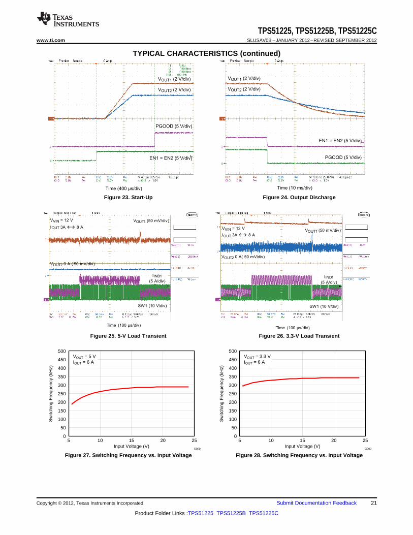
Figure 23. Start-Up Figure 24. Output Discharge
Figure 25. 5-V Load Transient Figure 26. 3.3-V Load Transient
Figure 27. Switching Frequency vs. Input Voltage Figure 28. Switching Frequency vs. Input Voltage
Copyright © 2012, Texas Instruments Incorporated Submit Documentation Feedback 21
Product Folder Links :TPS51225 TPS51225B TPS51225C
VIN
VBST1
U1
TPS51225
TPS51225 B
TPS51225C
DRVH1
SW1
12
17
16
18
0.1 µF
L1
C1
15.3 kW
DRVL115
VO114
VFB12
CS11
EN120
51 kW
10 kW
EN 5V
0.1 µF
0.1 µFVCLK19
VREG513
10 µF x 2
VIN
VOUT
5 V-8A
Charge-pump
Output
VBST2
DRVH2
SW2
9
10
8
DRVL2 11
VFB2 4
CS2 5
EN2 6
PGOOD 7
VREG3 3
10 µF x 2
0.1 µF
L2
C2
6.57 kW
47 kW
10 kW
EN 3.3 V
1 µF
VOUT
3.3 V - 8A
PGOOD
VREG
(3.3-V LDO)
UDG-12008
2.2 W
Q2
Q4
2.2 W
Q1
Q3
0.1 µF
GND
0.1 µF
VREG5
(5-V LDO)
1 µF
D1
TPS51225, TPS51225B, TPS51225CSLUSAV0B –JANUARY 2012–REVISED SEPTEMBER 2012 www.ti.com
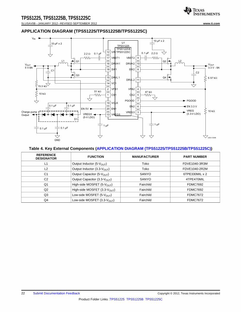
APPLICATION DIAGRAM (TPS51225/TPS51225B/TPS51225C)
Table 4. Key External Components (APPLICATION DIAGRAM (TPS51225/TPS51225B/TPS51225C))
REFERENCE FUNCTION MANUFACTURER PART NUMBERDESIGNATOR
L1 Output Inductor (5-VOUT) Toko FDVE1040-3R3M
L2 Output Inductor (3.3-VOUT) Toko FDVE1040-2R2M
C1 Output Capacitor (5-VOUT) SANYO 6TPE330MIL x 2
C2 Output Capacitor (3.3-VOUT) SANYO 4TPE470MIL
Q1 High-side MOSFET (5-VOUT) Fairchild FDMC7692
Q2 High-side MOSFET (3.3-VOUT) Fairchild FDMC7692
Q3 Low-side MOSFET (5-VOUT) Fairchild FDMC7672
Q4 Low-side MOSFET (3.3-VOUT) Fairchild FDMC7672
22 Submit Documentation Feedback Copyright © 2012, Texas Instruments Incorporated
Product Folder Links :TPS51225 TPS51225B TPS51225C

TPS51225, TPS51225B, TPS51225Cwww.ti.com SLUSAV0B –JANUARY 2012–REVISED SEPTEMBER 2012
Changes from Original (January 2012) to Revision A Page
• Deleted references to obsolete option TPS51225A throughout document .......................................................................... 1
Changes from Revision A (JUNE 2012) to Revision B Page
• Added specification for additional VVREG3 output voltage condition in ELECTIICAL CHARACTERISTICS table ................. 5
• Added clarity to the VREG5/VREG3 Linear Regulators section. ........................................................................................ 14
Copyright © 2012, Texas Instruments Incorporated Submit Documentation Feedback 23
Product Folder Links :TPS51225 TPS51225B TPS51225C
PACKAGE OPTION ADDENDUM
www.ti.com 24-Aug-2018
Addendum-Page 1
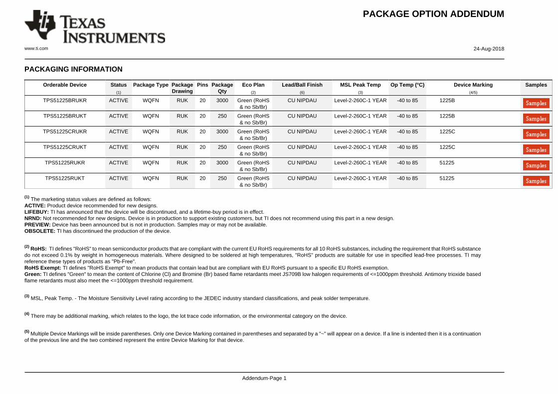
PACKAGING INFORMATION
Orderable Device Status(1)
Package Type PackageDrawing
Pins PackageQty
Eco Plan(2)
Lead/Ball Finish(6)
MSL Peak Temp(3)
Op Temp (°C) Device Marking(4/5)
Samples
TPS51225BRUKR ACTIVE WQFN RUK 20 3000 Green (RoHS& no Sb/Br)
CU NIPDAU Level-2-260C-1 YEAR -40 to 85 1225B
TPS51225BRUKT ACTIVE WQFN RUK 20 250 Green (RoHS& no Sb/Br)
CU NIPDAU Level-2-260C-1 YEAR -40 to 85 1225B
TPS51225CRUKR ACTIVE WQFN RUK 20 3000 Green (RoHS& no Sb/Br)
CU NIPDAU Level-2-260C-1 YEAR -40 to 85 1225C
TPS51225CRUKT ACTIVE WQFN RUK 20 250 Green (RoHS& no Sb/Br)
CU NIPDAU Level-2-260C-1 YEAR -40 to 85 1225C
TPS51225RUKR ACTIVE WQFN RUK 20 3000 Green (RoHS& no Sb/Br)
CU NIPDAU Level-2-260C-1 YEAR -40 to 85 51225
TPS51225RUKT ACTIVE WQFN RUK 20 250 Green (RoHS& no Sb/Br)
CU NIPDAU Level-2-260C-1 YEAR -40 to 85 51225
(1) The marketing status values are defined as follows:ACTIVE: Product device recommended for new designs.LIFEBUY: TI has announced that the device will be discontinued, and a lifetime-buy period is in effect.NRND: Not recommended for new designs. Device is in production to support existing customers, but TI does not recommend using this part in a new design.PREVIEW: Device has been announced but is not in production. Samples may or may not be available.OBSOLETE: TI has discontinued the production of the device.
(2) RoHS: TI defines "RoHS" to mean semiconductor products that are compliant with the current EU RoHS requirements for all 10 RoHS substances, including the requirement that RoHS substancedo not exceed 0.1% by weight in homogeneous materials. Where designed to be soldered at high temperatures, "RoHS" products are suitable for use in specified lead-free processes. TI mayreference these types of products as "Pb-Free".RoHS Exempt: TI defines "RoHS Exempt" to mean products that contain lead but are compliant with EU RoHS pursuant to a specific EU RoHS exemption.Green: TI defines "Green" to mean the content of Chlorine (Cl) and Bromine (Br) based flame retardants meet JS709B low halogen requirements of <=1000ppm threshold. Antimony trioxide basedflame retardants must also meet the <=1000ppm threshold requirement.
(3) MSL, Peak Temp. - The Moisture Sensitivity Level rating according to the JEDEC industry standard classifications, and peak solder temperature.
(4) There may be additional marking, which relates to the logo, the lot trace code information, or the environmental category on the device.
(5) Multiple Device Markings will be inside parentheses. Only one Device Marking contained in parentheses and separated by a "~" will appear on a device. If a line is indented then it is a continuationof the previous line and the two combined represent the entire Device Marking for that device.
PACKAGE OPTION ADDENDUM
www.ti.com 24-Aug-2018
Addendum-Page 2
(6) Lead/Ball Finish - Orderable Devices may have multiple material finish options. Finish options are separated by a vertical ruled line. Lead/Ball Finish values may wrap to two lines if the finishvalue exceeds the maximum column width.
Important Information and Disclaimer:The information provided on this page represents TI's knowledge and belief as of the date that it is provided. TI bases its knowledge and belief on informationprovided by third parties, and makes no representation or warranty as to the accuracy of such information. Efforts are underway to better integrate information from third parties. TI has taken andcontinues to take reasonable steps to provide representative and accurate information but may not have conducted destructive testing or chemical analysis on incoming materials and chemicals.TI and TI suppliers consider certain information to be proprietary, and thus CAS numbers and other limited information may not be available for release.
In no event shall TI's liability arising out of such information exceed the total purchase price of the TI part(s) at issue in this document sold by TI to Customer on an annual basis.

TAPE AND REEL INFORMATION
*All dimensions are nominal
Device PackageType
PackageDrawing
Pins SPQ ReelDiameter
(mm)
ReelWidth
W1 (mm)
A0(mm)
B0(mm)
K0(mm)
P1(mm)
W(mm)
Pin1Quadrant
TPS51225BRUKR WQFN RUK 20 3000 330.0 12.4 3.3 3.3 1.1 8.0 12.0 Q2
TPS51225BRUKT WQFN RUK 20 250 180.0 12.4 3.3 3.3 1.1 8.0 12.0 Q2
TPS51225CRUKR WQFN RUK 20 3000 330.0 12.4 3.3 3.3 1.1 8.0 12.0 Q2
TPS51225CRUKT WQFN RUK 20 250 180.0 12.4 3.3 3.3 1.1 8.0 12.0 Q2
TPS51225RUKR WQFN RUK 20 3000 330.0 12.4 3.3 3.3 1.1 8.0 12.0 Q2
TPS51225RUKT WQFN RUK 20 250 180.0 12.4 3.3 3.3 1.1 8.0 12.0 Q2
PACKAGE MATERIALS INFORMATION
www.ti.com 10-Sep-2016
Pack Materials-Page 1
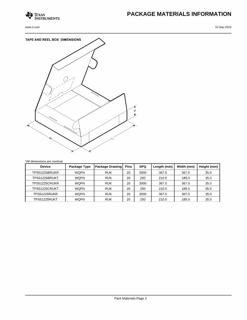
*All dimensions are nominal
Device Package Type Package Drawing Pins SPQ Length (mm) Width (mm) Height (mm)
TPS51225BRUKR WQFN RUK 20 3000 367.0 367.0 35.0
TPS51225BRUKT WQFN RUK 20 250 210.0 185.0 35.0
TPS51225CRUKR WQFN RUK 20 3000 367.0 367.0 35.0
TPS51225CRUKT WQFN RUK 20 250 210.0 185.0 35.0
TPS51225RUKR WQFN RUK 20 3000 367.0 367.0 35.0
TPS51225RUKT WQFN RUK 20 250 210.0 185.0 35.0
PACKAGE MATERIALS INFORMATION
www.ti.com 10-Sep-2016
Pack Materials-Page 2
IMPORTANT NOTICE
Texas Instruments Incorporated (TI) reserves the right to make corrections, enhancements, improvements and other changes to itssemiconductor products and services per JESD46, latest issue, and to discontinue any product or service per JESD48, latest issue. Buyersshould obtain the latest relevant information before placing orders and should verify that such information is current and complete.TI’s published terms of sale for semiconductor products (http://www.ti.com/sc/docs/stdterms.htm) apply to the sale of packaged integratedcircuit products that TI has qualified and released to market. Additional terms may apply to the use or sale of other types of TI products andservices.Reproduction of significant portions of TI information in TI data sheets is permissible only if reproduction is without alteration and isaccompanied by all associated warranties, conditions, limitations, and notices. TI is not responsible or liable for such reproduceddocumentation. Information of third parties may be subject to additional restrictions. Resale of TI products or services with statementsdifferent from or beyond the parameters stated by TI for that product or service voids all express and any implied warranties for theassociated TI product or service and is an unfair and deceptive business practice. TI is not responsible or liable for any such statements.Buyers and others who are developing systems that incorporate TI products (collectively, “Designers”) understand and agree that Designersremain responsible for using their independent analysis, evaluation and judgment in designing their applications and that Designers havefull and exclusive responsibility to assure the safety of Designers' applications and compliance of their applications (and of all TI productsused in or for Designers’ applications) with all applicable regulations, laws and other applicable requirements. Designer represents that, withrespect to their applications, Designer has all the necessary expertise to create and implement safeguards that (1) anticipate dangerousconsequences of failures, (2) monitor failures and their consequences, and (3) lessen the likelihood of failures that might cause harm andtake appropriate actions. Designer agrees that prior to using or distributing any applications that include TI products, Designer willthoroughly test such applications and the functionality of such TI products as used in such applications.TI’s provision of technical, application or other design advice, quality characterization, reliability data or other services or information,including, but not limited to, reference designs and materials relating to evaluation modules, (collectively, “TI Resources”) are intended toassist designers who are developing applications that incorporate TI products; by downloading, accessing or using TI Resources in anyway, Designer (individually or, if Designer is acting on behalf of a company, Designer’s company) agrees to use any particular TI Resourcesolely for this purpose and subject to the terms of this Notice.TI’s provision of TI Resources does not expand or otherwise alter TI’s applicable published warranties or warranty disclaimers for TIproducts, and no additional obligations or liabilities arise from TI providing such TI Resources. TI reserves the right to make corrections,enhancements, improvements and other changes to its TI Resources. TI has not conducted any testing other than that specificallydescribed in the published documentation for a particular TI Resource.Designer is authorized to use, copy and modify any individual TI Resource only in connection with the development of applications thatinclude the TI product(s) identified in such TI Resource. NO OTHER LICENSE, EXPRESS OR IMPLIED, BY ESTOPPEL OR OTHERWISETO ANY OTHER TI INTELLECTUAL PROPERTY RIGHT, AND NO LICENSE TO ANY TECHNOLOGY OR INTELLECTUAL PROPERTYRIGHT OF TI OR ANY THIRD PARTY IS GRANTED HEREIN, including but not limited to any patent right, copyright, mask work right, orother intellectual property right relating to any combination, machine, or process in which TI products or services are used. Informationregarding or referencing third-party products or services does not constitute a license to use such products or services, or a warranty orendorsement thereof. Use of TI Resources may require a license from a third party under the patents or other intellectual property of thethird party, or a license from TI under the patents or other intellectual property of TI.TI RESOURCES ARE PROVIDED “AS IS” AND WITH ALL FAULTS. TI DISCLAIMS ALL OTHER WARRANTIES ORREPRESENTATIONS, EXPRESS OR IMPLIED, REGARDING RESOURCES OR USE THEREOF, INCLUDING BUT NOT LIMITED TOACCURACY OR COMPLETENESS, TITLE, ANY EPIDEMIC FAILURE WARRANTY AND ANY IMPLIED WARRANTIES OFMERCHANTABILITY, FITNESS FOR A PARTICULAR PURPOSE, AND NON-INFRINGEMENT OF ANY THIRD PARTY INTELLECTUALPROPERTY RIGHTS. TI SHALL NOT BE LIABLE FOR AND SHALL NOT DEFEND OR INDEMNIFY DESIGNER AGAINST ANY CLAIM,INCLUDING BUT NOT LIMITED TO ANY INFRINGEMENT CLAIM THAT RELATES TO OR IS BASED ON ANY COMBINATION OFPRODUCTS EVEN IF DESCRIBED IN TI RESOURCES OR OTHERWISE. IN NO EVENT SHALL TI BE LIABLE FOR ANY ACTUAL,DIRECT, SPECIAL, COLLATERAL, INDIRECT, PUNITIVE, INCIDENTAL, CONSEQUENTIAL OR EXEMPLARY DAMAGES INCONNECTION WITH OR ARISING OUT OF TI RESOURCES OR USE THEREOF, AND REGARDLESS OF WHETHER TI HAS BEENADVISED OF THE POSSIBILITY OF SUCH DAMAGES.Unless TI has explicitly designated an individual product as meeting the requirements of a particular industry standard (e.g., ISO/TS 16949and ISO 26262), TI is not responsible for any failure to meet such industry standard requirements.Where TI specifically promotes products as facilitating functional safety or as compliant with industry functional safety standards, suchproducts are intended to help enable customers to design and create their own applications that meet applicable functional safety standardsand requirements. Using products in an application does not by itself establish any safety features in the application. Designers mustensure compliance with safety-related requirements and standards applicable to their applications. Designer may not use any TI products inlife-critical medical equipment unless authorized officers of the parties have executed a special contract specifically governing such use.Life-critical medical equipment is medical equipment where failure of such equipment would cause serious bodily injury or death (e.g., lifesupport, pacemakers, defibrillators, heart pumps, neurostimulators, and implantables). Such equipment includes, without limitation, allmedical devices identified by the U.S. Food and Drug Administration as Class III devices and equivalent classifications outside the U.S.TI may expressly designate certain products as completing a particular qualification (e.g., Q100, Military Grade, or Enhanced Product).Designers agree that it has the necessary expertise to select the product with the appropriate qualification designation for their applicationsand that proper product selection is at Designers’ own risk. Designers are solely responsible for compliance with all legal and regulatoryrequirements in connection with such selection.Designer will fully indemnify TI and its representatives against any damages, costs, losses, and/or liabilities arising out of Designer’s non-compliance with the terms and provisions of this Notice.
Mailing Address: Texas Instruments, Post Office Box 655303, Dallas, Texas 75265Copyright © 2018, Texas Instruments Incorporated