Slow-Light Photonic Crystal Devices
192
Karlsruhe Series in Photonics & Communications, Vol. 4 Jan-Michael Brosi Slow-Light Photonic Crystal Devices for High-Speed Optical Signal Processing
-
Upload
maryamsamir -
Category
Documents
-
view
81 -
download
2
description
طرق تسريع الاشارات الضوئية
Transcript of Slow-Light Photonic Crystal Devices
www.uvka.de
ISBN: 978-3-86644-313-6ISSN: 1865-1100 Ja
n-M
icha
el B
rosi
S
low
-Lig
ht P
C D
evic
es fo
r Hig
h-S
peed
Opt
ical
Sig
nal P
roce
ssin
g
4
Karlsruhe Series in Photonics & Communications, Vol. 4Edited by Prof. J. Leuthold and Prof. W. FreudeUniversität Karlsruhe (TH)Institute of High-Frequency and Quantum Electronics (IHQ)Germany
Karlsruhe Series in Photonics & Communications, Vol. 4
Photonic crystals are nano-optical devices that have the potential to slow down the propagation of light. “Slow light” is not only useful for generating true time delays, but is also good for enhancing nonlinear effects. With photonic crystals it is basically possible to tailor dispersion. Devices can be integrated in silicon-on-insulator photonic chips and could also be combined with electronics. For fabrication, the well-established CMOS process is available.
This book discusses design, modeling, and the characterization of fabricated slow-light photonic crystal waveguides, where applications aim for high-speed optical signal processing. Slow-light photonic crystal waveguides are fabrica-ted both at optical and microwave frequencies. Microwave model measure-ments serve as a highly accurate reference, based on which various numerical methods for calculating photonic crystals are evaluated and compared. Guide-lines are developed to obtain slow-light waveguides with broadband characte-ristics. Losses by fabrication imperfections are numerically determined and minimized. Nonlinearities are enhanced by a proper waveguide design and by additionally employing nonlinear organic materials. Three functional devices are proposed and studied: A tunable dispersion compensator, a tunable opti-cal delay line, and a high-speed electro-optic modulator. Optical measure-ments confirm the designs.
About the AuthorJan-Michael Brosi was born in 1978 in Filderstadt, Germany. In 2002 he recei-ved the M.Sc. degree in Electrical Engineering from Georgia Institute of Tech-nology, Atlanta, USA, and in 2008 the Dr.-Ing. (Ph.D.) degree from University of Karlsruhe, Germany. His research is focused on modeling, processing and characterization of photonic crystals and integrated optical devices.
Jan-Michael Brosi
Slow-Light Photonic Crystal Devices for High-SpeedOptical Signal Processing


Jan-Michael Brosi
Slow-Light Photonic Crystal Devicesfor High-Speed Optical Signal Processing

Karlsruhe Series in Photonics & Communications, Vol. 4Edited by Prof. J. Leuthold and Prof. W. Freude
Universität Karlsruhe (TH), Institute of High-Frequency and Quantum Electronics (IHQ), Germany

Slow-Light Photonic CrystalDevices for High-SpeedOptical Signal Processing
by Jan-Michael Brosi
Universitätsverlag Karlsruhe 2009 Print on Demand
ISSN: 1865-1100ISBN: 978-3-86644-313-6
Impressum
Universitätsverlag Karlsruhec/o UniversitätsbibliothekStraße am Forum 2D-76131 Karlsruhewww.uvka.de
Dieses Werk ist unter folgender Creative Commons-Lizenz lizenziert: http://creativecommons.org/licenses/by-nc-nd/2.0/de/
Dissertation, Universität Karlsruhe (TH)Fakultät für Elektrotechnik und Informationstechnik, 2008


Slow-Light Photonic Crystal Devices forHigh-Speed Optical Signal Processing
Zur Erlangung des akademischen Grades eines
DOKTOR-INGENIEURS
von der Fakultat furElektrotechnik und Informationstechnik
der Universitat Karlsruhe (TH)
genehmigte
DISSERTATION
von
Jan-Michael Brosi, M. Sc.
geboren in Filderstadt
Tag der mundlichen Prufung: 18. Juli 2008Hauptreferent: Prof. Dr.-Ing. Dr. h. c. Wolfgang FreudeKorreferenten: Prof. Dr. sc. nat. Jurg Leuthold
Prof. Dr. rer. nat. Ulrich Lemmer

Contents
Zusammenfassung (Deutsch) 1
Achievements and Limitations 5
Summary 9
1 Fundamentals 131.1 Wave Propagation in Dielectric Media . . . . . . . . . . . . . . . . . . . . . . 14
1.1.1 Maxwell’s Equations and Scaling Laws . . . . . . . . . . . . . . . . . 141.1.2 Modes of Translational Invariant Waveguides . . . . . . . . . . . . . . 15
1.2 2D Photonic Crystals . . . . . . . . . . . . . . . . . . . . . . . . . . . . . . . 171.2.1 Bulk Photonic Crystal . . . . . . . . . . . . . . . . . . . . . . . . . . 171.2.2 Photonic Crystal Waveguide . . . . . . . . . . . . . . . . . . . . . . . 19
1.3 Group Velocity and Chromatic Dispersion . . . . . . . . . . . . . . . . . . . . 201.4 Mode Gaps and Mini-Stop Bands in PC Waveguides . . . . . . . . . . . . . . 221.5 Excitation of Modes . . . . . . . . . . . . . . . . . . . . . . . . . . . . . . . . 241.6 Losses in Photonic Crystals . . . . . . . . . . . . . . . . . . . . . . . . . . . . 251.7 Tuning of Photonic Crystals . . . . . . . . . . . . . . . . . . . . . . . . . . . 27
1.7.1 Thermal Tuning . . . . . . . . . . . . . . . . . . . . . . . . . . . . . . 271.7.2 Free-Carrier Injection . . . . . . . . . . . . . . . . . . . . . . . . . . . 271.7.3 Electro-Optic Effect . . . . . . . . . . . . . . . . . . . . . . . . . . . 28
2 Slow-Light Waveguides 312.1 Design . . . . . . . . . . . . . . . . . . . . . . . . . . . . . . . . . . . . . . . 32
2.1.1 Waveguide Geometries . . . . . . . . . . . . . . . . . . . . . . . . . . 32Line-Defect Waveguide . . . . . . . . . . . . . . . . . . . . . . . . 33Slot Waveguide . . . . . . . . . . . . . . . . . . . . . . . . . . . . 34Center-Hole Waveguide . . . . . . . . . . . . . . . . . . . . . . . . 35
2.1.2 Design Principles . . . . . . . . . . . . . . . . . . . . . . . . . . . . . 362.1.3 Group Velocity and Dispersion Engineering . . . . . . . . . . . . . . . 39
Broadband Slow Light . . . . . . . . . . . . . . . . . . . . . . . . . 39Negative Chromatic Dispersion . . . . . . . . . . . . . . . . . . . . 40
2.1.4 Efficient Mode Excitation . . . . . . . . . . . . . . . . . . . . . . . . 41Adiabatic Tapers . . . . . . . . . . . . . . . . . . . . . . . . . . . . 41Counter-Propagating Mode Coupling . . . . . . . . . . . . . . . . . 43
i
ii CONTENTS
2.1.5 Conclusion . . . . . . . . . . . . . . . . . . . . . . . . . . . . . . . . 452.2 Imperfections . . . . . . . . . . . . . . . . . . . . . . . . . . . . . . . . . . . 47
2.2.1 Loss Parameters and Loss Model . . . . . . . . . . . . . . . . . . . . 482.2.2 Numerical Methods . . . . . . . . . . . . . . . . . . . . . . . . . . . . 502.2.3 Broadband Slow-Light Structures . . . . . . . . . . . . . . . . . . . . 502.2.4 Loss Simulation Results . . . . . . . . . . . . . . . . . . . . . . . . . 52
FIT Method . . . . . . . . . . . . . . . . . . . . . . . . . . . . . . 54GME Method . . . . . . . . . . . . . . . . . . . . . . . . . . . . . 57Comparison . . . . . . . . . . . . . . . . . . . . . . . . . . . . . . 58
2.2.5 Dependance of Losses on Group Velocity . . . . . . . . . . . . . . . . 592.2.6 Conclusion . . . . . . . . . . . . . . . . . . . . . . . . . . . . . . . . 61
3 Devices 633.1 Tunable Dispersion Compensator . . . . . . . . . . . . . . . . . . . . . . . . . 63
3.1.1 Principle of Operation . . . . . . . . . . . . . . . . . . . . . . . . . . 643.1.2 PC-WG Design . . . . . . . . . . . . . . . . . . . . . . . . . . . . . . 663.1.3 Simulation of Device Characteristics . . . . . . . . . . . . . . . . . . . 673.1.4 Conclusion . . . . . . . . . . . . . . . . . . . . . . . . . . . . . . . . 68
3.2 Tunable Optical Delay Line . . . . . . . . . . . . . . . . . . . . . . . . . . . . 693.2.1 Principle of Operation . . . . . . . . . . . . . . . . . . . . . . . . . . 693.2.2 PC-WG Design . . . . . . . . . . . . . . . . . . . . . . . . . . . . . . 71
Constant Negative Chromatic Dispersion . . . . . . . . . . . . . . . 71Constant Positive Chromatic Dispersion . . . . . . . . . . . . . . . 72
3.2.3 Optimization . . . . . . . . . . . . . . . . . . . . . . . . . . . . . . . 733.2.4 Conclusion . . . . . . . . . . . . . . . . . . . . . . . . . . . . . . . . 75
3.3 Compact High-Speed Electro-Optic Modulator . . . . . . . . . . . . . . . . . 773.3.1 The Modulator . . . . . . . . . . . . . . . . . . . . . . . . . . . . . . 773.3.2 Mach-Zehnder Optimization Strategy . . . . . . . . . . . . . . . . . . 793.3.3 Slow-Wave Phase Modulator . . . . . . . . . . . . . . . . . . . . . . . 79
PC Slot Waveguide . . . . . . . . . . . . . . . . . . . . . . . . . . 80PC Slot Waveguide with Dispersion Engineering . . . . . . . . . . . 81
3.3.4 Modulator Performance Parameters . . . . . . . . . . . . . . . . . . . 81Modulation Bandwidth of Mach-Zehnder Modulator . . . . . . . . . 81π-Voltage Uπ of Phase Modulator . . . . . . . . . . . . . . . . . . . 83
3.3.5 Optimized Mach-Zehnder Modulator . . . . . . . . . . . . . . . . . . 843.3.6 Slow-Light Coupling Structure . . . . . . . . . . . . . . . . . . . . . . 853.3.7 Conclusion . . . . . . . . . . . . . . . . . . . . . . . . . . . . . . . . 86
4 Experiments and Modeling 894.1 Optical Experiments . . . . . . . . . . . . . . . . . . . . . . . . . . . . . . . 89
4.1.1 Measurement Setups . . . . . . . . . . . . . . . . . . . . . . . . . . . 904.1.2 Strip Waveguide . . . . . . . . . . . . . . . . . . . . . . . . . . . . . 914.1.3 Broadband Slow Light Waveguide . . . . . . . . . . . . . . . . . . . . 934.1.4 Waveguide with Linearly Varying Chromatic Dispersion . . . . . . . . 954.1.5 Slot Waveguide . . . . . . . . . . . . . . . . . . . . . . . . . . . . . . 97
CONTENTS iii
4.1.6 Conclusion . . . . . . . . . . . . . . . . . . . . . . . . . . . . . . . . 994.2 Microwave Experiments . . . . . . . . . . . . . . . . . . . . . . . . . . . . . 101
4.2.1 Microwave Model . . . . . . . . . . . . . . . . . . . . . . . . . . . . 102Dielectric Microwave Materials . . . . . . . . . . . . . . . . . . . . 102Excitation of the Waveguide Mode . . . . . . . . . . . . . . . . . . 102Material Characterization . . . . . . . . . . . . . . . . . . . . . . . 104
4.2.2 Broadband Slow Light Waveguide . . . . . . . . . . . . . . . . . . . . 105Structure and Design . . . . . . . . . . . . . . . . . . . . . . . . . . 105Device Characteristics . . . . . . . . . . . . . . . . . . . . . . . . . 106Pulse Transmission and Delay-Bandwidth Product . . . . . . . . . . 108Field Distribution . . . . . . . . . . . . . . . . . . . . . . . . . . . 109Disorder Influence . . . . . . . . . . . . . . . . . . . . . . . . . . . 109
4.2.3 Conclusion . . . . . . . . . . . . . . . . . . . . . . . . . . . . . . . . 1124.3 Verification of Numerics . . . . . . . . . . . . . . . . . . . . . . . . . . . . . 113
4.3.1 Benchmark of Different Design Tools . . . . . . . . . . . . . . . . . . 1134.3.2 Simulation of Disorder-Induced Losses . . . . . . . . . . . . . . . . . 114
Numerical Calibration Procedure . . . . . . . . . . . . . . . . . . . 115Comparison of Ensemble Averaged Results . . . . . . . . . . . . . . 116Comparison of Single Realization . . . . . . . . . . . . . . . . . . . 117
4.3.3 Conclusion . . . . . . . . . . . . . . . . . . . . . . . . . . . . . . . . 117
Appendix 119A.1 Mathematical Transformations and Signal Representation . . . . . . . . . . . . 119
A.1.1 Fourier Transform . . . . . . . . . . . . . . . . . . . . . . . . . . . . 119A.1.2 Signal Representation . . . . . . . . . . . . . . . . . . . . . . . . . . 119A.1.3 Laplace Transform . . . . . . . . . . . . . . . . . . . . . . . . . . . . 120
A.2 Numerical Modeling Tools . . . . . . . . . . . . . . . . . . . . . . . . . . . . 121A.3 Mode Orthogonality and Group Velocity . . . . . . . . . . . . . . . . . . . . . 123A.4 Through-Reflect-Line (TRL) Calibration . . . . . . . . . . . . . . . . . . . . . 127A.5 Coupling of Counter-Propagating Modes . . . . . . . . . . . . . . . . . . . . . 131A.6 Loss Modeling . . . . . . . . . . . . . . . . . . . . . . . . . . . . . . . . . . 135A.7 Determination of Modulator Characteristics . . . . . . . . . . . . . . . . . . . 137
A.7.1 Propagation Equation and Field Interaction Factor Γ . . . . . . . . . . 137A.7.2 Modulator Walk-Off Bandwidth . . . . . . . . . . . . . . . . . . . . . 137A.7.3 Modulator Bandwidth Limitations by RC-Effects . . . . . . . . . . . . 138
A.8 Microwave Measurement Techniques . . . . . . . . . . . . . . . . . . . . . . 141A.8.1 Continuous Wave Measurements . . . . . . . . . . . . . . . . . . . . . 141A.8.2 Pulse Measurements . . . . . . . . . . . . . . . . . . . . . . . . . . . 142A.8.3 Near-Field Measurements . . . . . . . . . . . . . . . . . . . . . . . . 143
Glossary 145Acronyms . . . . . . . . . . . . . . . . . . . . . . . . . . . . . . . . . . . . . . . . 145Symbols . . . . . . . . . . . . . . . . . . . . . . . . . . . . . . . . . . . . . . . . . 147
Bibliography 161

iv CONTENTS
Acknowledgments 163
List of Own Publications 165
Curriculum Vitae 169
List of Figures
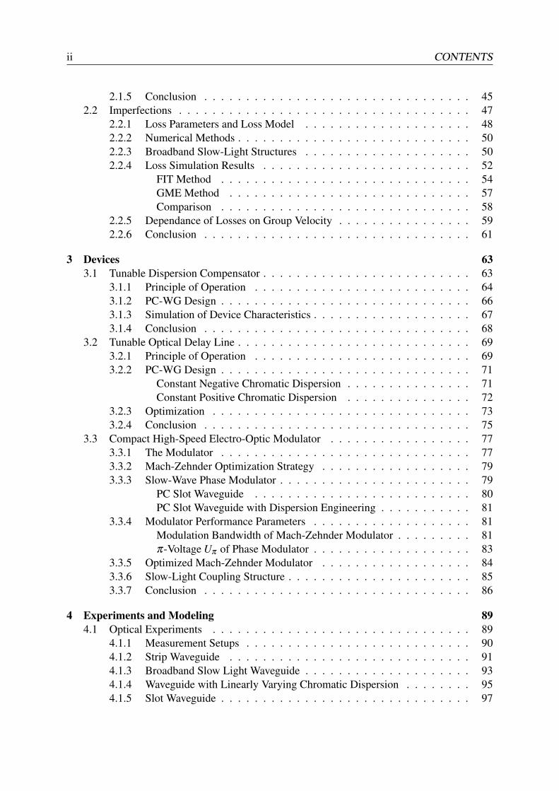
1.1 Schematic of a strip waveguide. . . . . . . . . . . . . . . . . . . . . . . . . . 151.2 Dispersion relation of a SOI waveguide. . . . . . . . . . . . . . . . . . . . . . 161.3 Schematic of a PC and a PC-WG. . . . . . . . . . . . . . . . . . . . . . . . . 171.4 Direct and reciprocal lattice of a 2D-PC. . . . . . . . . . . . . . . . . . . . . . 181.5 Band diagram of a bulk PC. . . . . . . . . . . . . . . . . . . . . . . . . . . . . 191.6 Band diagram of a line defect PC-WG. . . . . . . . . . . . . . . . . . . . . . . 201.7 Group velocity and chromatic dispersion of a PC-WG. . . . . . . . . . . . . . 221.8 Formation of mode gaps and mini-stop bands in a PC. . . . . . . . . . . . . . . 231.9 Band diagram of a multi-moded PC-WG. . . . . . . . . . . . . . . . . . . . . 241.10 Coupling schemes from a strip WG to a PC-WG. . . . . . . . . . . . . . . . . 251.11 Extrinsic losses in a PC-WG. . . . . . . . . . . . . . . . . . . . . . . . . . . . 27
2.1 Structure parameters of a line-defect PC-WG. . . . . . . . . . . . . . . . . . . 332.2 Band diagram of a W1 line defect PC-WG . . . . . . . . . . . . . . . . . . . . 332.3 Structure parameters of a slot PC-WG. . . . . . . . . . . . . . . . . . . . . . . 342.4 Band diagram of a slot PC-WG. . . . . . . . . . . . . . . . . . . . . . . . . . 352.5 Structure parameters of a center-hole PC-WG. . . . . . . . . . . . . . . . . . . 352.6 Band diagram of a center-hole PC-WG. . . . . . . . . . . . . . . . . . . . . . 362.7 Effect of structure parameter variation on the mode band of a W1-WG. . . . . . 372.8 Broadband slow light PC-WG. . . . . . . . . . . . . . . . . . . . . . . . . . . 392.9 PC-WG with negative chromatic dispersion. . . . . . . . . . . . . . . . . . . . 402.10 Center-hole PC-WG with negative chromatic dispersion. . . . . . . . . . . . . 412.11 Local modes of a PC taper. . . . . . . . . . . . . . . . . . . . . . . . . . . . . 422.12 Coupling taper for efficient slow-light excitation. . . . . . . . . . . . . . . . . 432.13 Coupling of a center-hole WG to a line-defect WG. . . . . . . . . . . . . . . . 442.14 Counter-propagating mode excitation of center-hole WG. . . . . . . . . . . . . 452.15 Loss model for a PC-WG. . . . . . . . . . . . . . . . . . . . . . . . . . . . . 492.16 Structure schematics for broadband slow light designs. . . . . . . . . . . . . . 522.17 Band diagrams of broadband slow light structures. . . . . . . . . . . . . . . . . 532.18 Group velocity for broadband slow light designs. . . . . . . . . . . . . . . . . 542.19 Transmission with and without disorder from FIT. . . . . . . . . . . . . . . . . 552.20 Group velocity for disordered structures from FIT. . . . . . . . . . . . . . . . . 552.21 Normalized transmission and reflection for disordered structures from FIT. . . . 562.22 Loss parameters for broadband slow light WGs from FIT. . . . . . . . . . . . . 572.23 Losses for broadband slow light WGs from GME. . . . . . . . . . . . . . . . . 58
v
vi LIST OF FIGURES
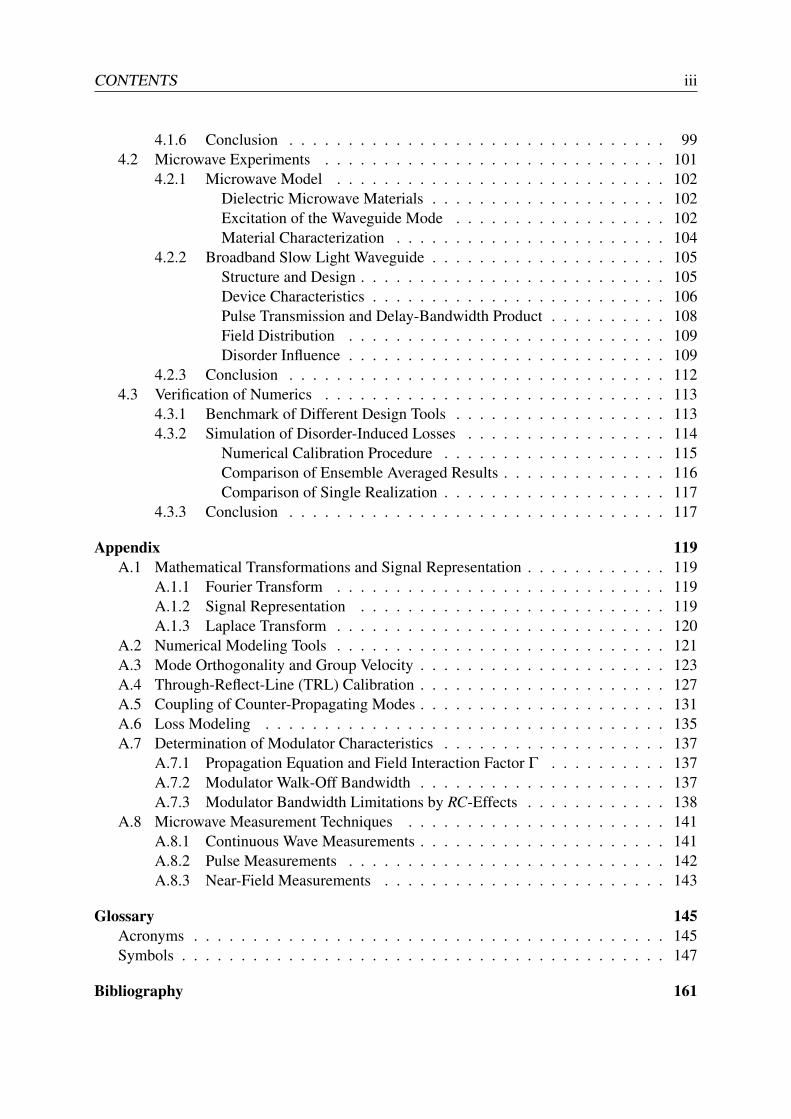
2.24 Comparison of losses from GME and FIT. . . . . . . . . . . . . . . . . . . . . 592.25 Dependance of total losses on group index. . . . . . . . . . . . . . . . . . . . 60
3.1 Chromatic dispersion of basic PC-WG for dispersion compensator. . . . . . . . 653.2 Structure schematic of tunable dispersion compensator. . . . . . . . . . . . . . 653.3 PC-WGs for tunable dispersion compensator. . . . . . . . . . . . . . . . . . . 663.4 Total dispersion of tunable dispersion compensator. . . . . . . . . . . . . . . . 673.5 Transmission, reflection and dispersion of dispersion compensator. . . . . . . . 683.6 Group delay of a PC-WG of constant chromatic dispersion. . . . . . . . . . . . 703.7 Group delay of two concatenated WG sections of constant dispersion. . . . . . 703.8 Structure schematic of tunable delay line. . . . . . . . . . . . . . . . . . . . . 713.9 PC-WG devices with constant negative chromatic dispersion. . . . . . . . . . . 723.10 Principle to obtain constant positive chromatic dispersion. . . . . . . . . . . . 733.11 PC-WG devices with constant positive chromatic dispersion. . . . . . . . . . . 743.12 Mach-Zehnder modulator schematic. . . . . . . . . . . . . . . . . . . . . . . . 783.13 Phase modulator schematic and dominant electric field component. . . . . . . . 803.14 Band diagram of W1.4 PC slot waveguide. . . . . . . . . . . . . . . . . . . . . 813.15 Structure parameters and group velocity of W1.25 PC slot waveguide. . . . . . 823.16 Schematic of the coupling structure from strip-WG to slot PC-WG. . . . . . . . 853.17 Transmission and reflection for the transition from slot-WG to PC-WG. . . . . 86
4.1 Measurement setups for optical device characterization. . . . . . . . . . . . . . 904.2 SEM photograph of strip WG. . . . . . . . . . . . . . . . . . . . . . . . . . . 924.3 Measured transmission of strip-WG. . . . . . . . . . . . . . . . . . . . . . . . 924.4 Measured losses of strip WG. . . . . . . . . . . . . . . . . . . . . . . . . . . . 934.5 SEM photograph of broadband slow-light WG. . . . . . . . . . . . . . . . . . 944.6 Measured transmission of broadband slow light PC-WG. . . . . . . . . . . . . 944.7 Measured group delay of broadband slow-light WG compared to simulation. . . 954.8 SEM photograph of broadband slow-light WG. . . . . . . . . . . . . . . . . . 964.9 Measured transmission of PC-WG with linearly varying dispersion. . . . . . . 964.10 Measured group delay of PC-WG with linearly varying dispersion compared to
simulation. . . . . . . . . . . . . . . . . . . . . . . . . . . . . . . . . . . . . 974.11 SEM photograph of slow-light slot WG and of coupling structure. . . . . . . . 984.12 Measured transmission of PC-WG with linearly varying dispersion. . . . . . . 984.13 Measured group delay of PC-WG with linearly varying dispersion compared to
simulation. . . . . . . . . . . . . . . . . . . . . . . . . . . . . . . . . . . . . 994.14 Exploded view of the microstrip-fed slot antenna. . . . . . . . . . . . . . . . . 1034.15 Broadband slot antenna to excite strip-WG mode near 10GHz. . . . . . . . . . 1034.16 Measured effective refractive index of strip-WG compared to simulation. . . . . 1044.17 Band diagram of PC-WG with a slow light region and a flat band. . . . . . . . 1064.18 Schematic of the PC device and reference measurement. . . . . . . . . . . . . 1064.19 Transmission and reflection spectra of the PC device. . . . . . . . . . . . . . . 1074.20 Group velocity and chromatic dispersion of the PC-WG. . . . . . . . . . . . . 1074.21 Delay of a broadband pulse in a PC-WG and inferred group velocity. . . . . . 1084.22 Measured and simulated field distribution at low and high group velocity. . . . 110
LIST OF FIGURES vii
4.23 Group velocity and transmission of disordered microwave model samples. . . . 1114.24 Comparison of measurements to FIT simulations for a disordered structure. . . 1114.25 Group velocity from different methods to calculate band diagrams. . . . . . . . 1144.26 TRL calibration structures for disorder simulations. . . . . . . . . . . . . . . . 1154.27 Comparison of FIT and FDTD results for disordered structures. . . . . . . . . . 1164.28 Comparison of FIT and GME results for disordered structures . . . . . . . . . 1174.29 Comparison of FIT and FDTD results for a disordered realization. . . . . . . . 118
A.1 TRL calibration scheme. . . . . . . . . . . . . . . . . . . . . . . . . . . . . . 127A.2 Parallel-coupling of two PC-WGs with counter-propagating modes. . . . . . . 133A.3 Electrical modulator RC-effects. . . . . . . . . . . . . . . . . . . . . . . . . . 139A.4 Notation for a two-port device. . . . . . . . . . . . . . . . . . . . . . . . . . . 141A.5 Measurement setup for the three standards needed for TRL calibration. . . . . . 142A.6 Measurement setup for pulse transmission in the microwave model. . . . . . . 143A.7 Measurement setup for the 2D near-field distribution. . . . . . . . . . . . . . . 144

viii LIST OF FIGURES
List of Tables
2.1 Structure parameters for broadband slow light designs. . . . . . . . . . . . . . 51
3.1 Characteristic data for a PC slot waveguide modulator. . . . . . . . . . . . . . 84
4.1 Properties of microwave materials at 10GHz. . . . . . . . . . . . . . . . . . . 1024.2 Runtime and memory usage for band diagram methods. . . . . . . . . . . . . . 114
ix

x LIST OF TABLES
Zusammenfassung (Deutsch)
In dieser Arbeit werden nanophotonische Bauteile auf Basis von photonischen Kristallen mitniedriger Ausbreitungsgeschwindigkeit des Lichtes untersucht. Die Bauteile sollen in der op-tischen Signalverarbeitung bei hohen Bitraten Anwendung finden. Neuartige Bauteil-Konzeptewerden entwickelt, numerische Entwurfe und Simulationen vorgestellt, und Experimente anoptischen Bauteilen und an vergroßerten Mikrowellenmodellen ausgefuhrt.
Durch das rasante Wachstum des Internet-Datenverkehrs und der mobilen Datenkommuni-kation nehmen die Geschwindigkeits-Anforderungen an Kommunikationsverbindungen standigzu. Die Kapazitat von Kupfer-Leitungen oder Funkverbindungen ist allerdings grundlegendbegrenzt, so dass sehr hohe Datenraten nur uber kurze Distanzen ubertragen werden konnen.Abhilfe konnen hier vor allem optische Datenverbindungen schaffen, die um ein Vielfachesgroßere Kapazitaten zur Verfugung stellen. Tatsachlich ist es zu beobachten dass immer mehroptische Kommunikationstechnik zum Einsatz kommt und dass die optischen Verbindungenimmer naher an den Endverbraucher heranrucken. Daneben wird auch schon untersucht, Optikzur Ubertragung uber kleinste Distanzen, wie z. B. innerhalb von Mikrochips, zu verwenden.
Die Kosten und die Große von funktionalen optischen Komponenten konnten erheblich re-duziert werden, wenn integrierte optische Bauteile eingesetzt werden. Insbesondere die Silizi-um-Optik ist dabei von großem Interesse, denn die naturlichen Silizium-Rohstoffe sind nahezuunerschopflich, es konnen die gleichen Fabrikationsprozesse wie fur Mikro-Chips angewendetwerden, und es ist prinzipiell moglich sowohl elektronische als auch optische Komponentenauf ein und demselben Chip zu kombinieren. Silizium besitzt zudem einen hohen optischenBrechungsindexkontrast gegnuber Luft, der die benotigten Wellenleiterabmessungen und damitdie Chipflache reduziert. Der hohe Indexkontrast ermoglicht außerdem die Entwicklung vonplanaren photonischen Kristallen mit einer photonischen Bandlucke.
Ein photonischer Kristall ist eine dielektrische periodische Struktur, die meist kunstlich her-gestellt wird. In unserem Fall wird eine dunne Silizium-Schicht mit regelmaßig angeordnetenzylindrischen Lochern versehen, so dass eine zweidimensionale Periodizitat entsteht. Die be-sondere Eigenschaft eines photonischen Kristalls ist es, dass eine polarisationsabhangige pho-tonische Bandlucke entstehen kann. Das hat zur Folge, dass sich Licht einer bestimmten Polari-sation und Frequenz in der Schichtstruktur nicht ausbreiten kann. Wird in einen idealen Kristallein Defekt-Wellenleiter eingefugt, so kann das Licht darin sehr effektiv gefuhrt werden, und esentstehen zudem Frequenzbereiche mit sehr niedriger Gruppengeschwindigkeit oder sehr hoherchromatischer Dispersion. Diese Eigenschaften wollen wir nutzen, um funktionale Komponen-ten mit besonderen Eigenschaften fur die optische Kommunikationstechnik zu entwerfen.
Zu Beginn der Arbeit zeigen wir die grundlegenden Eigenschaften von photonischen Kris-tallen auf. Die Wellenausbreitung in photonischen Kristallen wird beschrieben, und dazu wer-
1
2 Zusammenfassung (Deutsch)
den Banddiagramme eingefuhrt. Erreicht ein Modus im photonischen Kristall-Wellenleiter denRand des Banddiagramms, geht die Gruppengeschwindigkeit gegen Null, wahrend die chro-matische Dispersion stark anwachst. Dieses Verhalten entsteht durch die Interaktion zweierursprunglich entgegenlaufender Moden. Wir diskutieren im Weiteren die Anregung von Modenin photonischen Kristallen, und sprechen Verlust-Mechanismen an. Um die Eigenschaften vonphotonischen Kristallen extern beeinflussen zu konnen zeigen wir verschiedene Methoden auf.
Anschließend befassen wir uns ausfuhrlich mit dem Entwurf von Wellenleitern in photoni-schen Kristallen, die eine langsame Lichtausbreitung ermoglichen. Unterschiedliche Wellenlei-terstrukturen werden vorgestellt, und Strategien werden entwickelt, um die Gruppengeschwin-digkeit oder die chromatische Dispersion durch Veranderung von Strukturparametern einzustel-len. Als Beispiele prasentieren wir einen Wellenleiter, der eine kleine Gruppengeschwindigkeitvon 4% der Vakuum-Lichtgeschwindigkeit in einer Bandbreite von 2THz aufweist, und einenWellenleiter mit einer hohen negativen chromatischen Dispersion von −4.5ps/(mmnm). Umeinen Wellenleiter bei niedriger Gruppengeschwindigkeit effizient mit einem Streifen-Wellenlei-ter anregen zu konnen, entwerfen wir einen speziellen Koppel-Taper im photonischen Kris-tall. Daruber hinaus entwickeln wir eine Methode, um einen Modus mit negativer Gruppenge-schwindigkeit anzuregen.
Ungenauigkeiten bei der Herstellung von photonischen Kristallen sind unvermeidlich undfuhren zu erhohten Transmissionsverlusten, die die Leistungsfahigkeit maßgeblich beeintrachti-gen konnen. Wir untersuchen durch Simulationen, wie sich die Verluste in verschiedenen Wel-lenleitern bei langsamem Licht verhalten, und entwickeln Maßnahmen um diese Verluste zu mi-nimieren. Es zeigt sich, dass die geringsten Verluste in einer vertikal symmetrischen Membran-Struktur bei einer maximal moglichen Wellenleiterbreite fur einmodiges Verhalten auftreten.Eine vertikale Asymmetrie, bedingt z. B. durch unterschiedliche Materialien im Substrat und inder Deckschicht oder durch Fabrikations-Ungenauigkeiten, fuhrt zu Modenkopplung und damitzu erhohten Verlusten. Auch ein mehrmodiger Wellenleiter zeigt wesentlich großere Verlus-te durch Modenkopplung. Bei allen Strukturen wird die Gruppengeschwindigkeit nur unwe-sentlich durch die Unordnung beeinflusst. Desweiteren untersuchen wir den Zusammenhangzwischen der Große der Verluste und der Gruppengeschwindigkeit. Im Gegensatz zu fruherenStudien konnen wir aber keinen einfachen Zusammenhang der Verluste mit dem Gruppenbre-chungsindex bestatigen.
Die gewonnenen Einsichten und Entwurfsprinzipien werden weiter zur Entwicklung vondrei wichtigen Komponenten verwendet: Einem einstellbaren Dispersionskompensator, einereinstellbaren Verzogerungsleitung, und einem schnellen elektro-optischen Modulator.
Wir prasentieren einen Entwurf fur einen Dispersionskompensator mit einer regelbarenchromatischen Dispersion zwischen −19ps/(mmnm) und +7ps/(mmnm) in einer 125GHzgroßen Bandbreite. Der Kompensator besteht aus zwei hintereinander geschalteten photonischeKristall-Wellenleitern, in denen sich jeweils die Dispersion linear mit der Frequenz andert. DieVorzeichen der Steigungen unterscheiden sich dabei, und bei entsprechender Langenanpassungresultiert eine konstante Dispersion. Indem die Charakteristik einer der Sektionen in der Fre-quenz verschoben wird, z. B. durch Erhitzen, kann die Dispersion eingestellt werden.
Weiterhin entwickeln wir eine optische Verzogerungsleitung, die bei einer Bauteillange von1mm eine variable Verzogerung bis zu 42.2ps in einer Bandbreite von 125GHz erreichen kann.Die maximale Verzogerung entspricht dabei der Zeitdauer von 5 Pulsen eines 33% RZ Daten-Signals bei 40Gbit/s. Ahnlich wie beim Dispersions-Kompensator werden zwei photonische
Zusammenfassung (Deutsch) 3
Kristall-Wellenleiter hintereinander geschaltet, diesmal aber mit konstanter positiver bzw. kon-stanter negativer Dispersion. Durch eine Frequenz-Verschiebung einer der beiden Sektionenkann die Verzogerung eingestellt werden.
Der schnelle optische Modulator ist auf Basis eines photonischen Kristalls mit einem schma-len Spalt in der Mitte des Defektwellenleiters aufgebaut. In den Spalt kann ein stark elektro-optisches Material wie z. B. ein Polymer infiltriert werden, in dem eine Phasenverschiebungstattfinden kann. Wir prasentieren einen Modulator-Entwurf mit einer Modulationsbandbreitevon 78GHz und einer Lange von 80 µm bei einer Ansteuerspannung von nur 1V. Die Bandbrei-te erlaubt eine Datenrate von 100Gbit/s. Solche Werte konnen durch eine hohe Konzentrationvon sowohl dem optischen als auch dem elektrischen Feld auf den Spalt und durch eine niedrigeGruppengeschwindigkeit, die die nichtlineare Interaktion weiter verstarkt, erzielt werden.
Die Realisierbarkeit von breitbandigen photonischen Kristallen mit langsamer Lichtausbrei-tung zeigen wir durch Messergebnisse von Wellenleitern, die mit Deep-UV-Lithographie herge-stellt wurden. Eine zusatzliche Glas-Deckschicht sorgt fur einen vertikal symmetrischen Auf-bau. Es wird ein breitbandiger Wellenleiter mit einer Gruppengeschwindigkeit von 3.7% derVakuum-Lichtgeschwindigkeit, ein Wellenleiter mit linear variierender Dispersion und einemDispersions-Minimum von −5ps/(mmnm), und ein Schlitz-Wellenleiter bei niedriger Grup-pengeschwindigkeit vermessen. Die Gruppenverzogerungscharakteristiken stimmen gut mit denSimulationsergebnissen uberein, was die Umsetzbarkeit der Entwurfe beweist. Die minimalenTransmissionsverluste liegen fur die Wellenleiter zwischen 10dB/mm und 14dB/mm. Die-se relativ hohen Werte werden vor allem durch die schragen Seitenwande und durch Ober-flachen-Rauigkeiten hervorgerufen. Eine Weiterentwicklung des Fabrikationsprozesses konntediese Verluste verringern.
Um photonische Kristalle im Experiment mit wesentlich großerer Genauigkeit herstellenund charakterisieren zu konnen, entwickeln wir ein vergroßertes Mikrowellen-Modell. Dabeiwerden bei gleicher Brechzahl im Mikrowellenmodell die Strukturen um einen Faktor 20.000vergroßert und dafur die Betriebsfrequenz um denselben Faktor auf 10GHz verkleinert. Wirdemonstrieren einen photonischen Kristall-Wellenleiter, der umgerechnet auf den optischen Be-reich eine Region mit einer Gruppengeschwindigkeit von 4% der Vakuum-Lichtgeschwindigkeitund eine Region mit einer chromatischen Dispersion von 4ps/(mmnm) aufweist, jeweils ineiner Bandbreite von 1THz. Die Experimente bestatigen dabei die Simulationen mit der Finite-integration-technique (FIT) sehr gut. Weiterhin konnen wir am Mikrowellenmodell zeigen, dasszufallige 5-prozentige Storungen der Locher-Radien die Gruppengeschwindigkeit nicht maß-geblich beeintrachtigen.
Auf Basis der Mikrowellen-Modellexperimente ist es außerdem moglich, verschiedene nu-merische Werkzeuge zum Entwurf von photonischen Kristall-Wellenleitern zu vergleichen. Wirermitteln dabei ein akkurates und schnelles Werkzeug fur den Entwurf, namlich die Guided-mode-expansion-Methode (GME). Schließlich wird die Simulation fur die Bestimmung derVerluste durch Fabrikations-Ungenauigkeiten uberpruft. Dabei stellt sich die FIT Methode alsbesonders zuverlassig heraus.

4 Zusammenfassung (Deutsch)
Achievements and Limitations
In this work, we study slow-light photonic crystal (PC) waveguides (WGs) in silicon and in-vestigate the potential to realize powerful, cheap and small components for high-speed opticalsignal processing. Novel device concepts are developed, extensive numerical designs and sim-ulations are performed, and optical experiments as well as scaled microwave experiments areconducted. In this chapter, we summarize our achievements and comment on the limitations ofphotonic crystal devices.
Group Velocity and Dispersion Engineering: We develop detailed design procedures to en-gineer the group velocity and chromatic dispersion characteristics of PC-WGs by ap-propriately changing the structure parameters. Broadband slow light WGs with a groupvelocity below 4% of the vacuum speed of light and low chromatic dispersion in a band-width of more than 1THz are designed. PC-WGs with high negative chromatic dispersionwell below −5ps/(mmnm) and with spectral ranges of linearly increasing and decreas-ing dispersion characteristics are developed.
Improved Mode Excitation: We advance a PC coupling taper to significantly improve the ex-citation of the slow-light PC mode with a strip-WG. Along the taper, selected structureparameters are continuously changed to gradually slow down the PC. The losses perinterface can be decreases below −0.5dB, and the reflection can be reduced to a valuesmaller than −10dB. Furthermore, a coupling concept is presented that allows exciting amode with high negative dispersion by injecting power inside a mini-stop band.
Understanding and Minimizing Disorder-Induced Losses: We numerically determine dis-order-induced losses of various broadband slow-light PC-WGs. The numerical tools arecarefully evaluated, and a loss model is introduced that is needed to analyze the results.We find procedures to minimize losses, and the lowest losses can be found in an airmembrane structure with a WG core width as large as possible to still be single-moded.Multi-moded or vertically asymmetric PC-WGs exhibit strong mode-coupling effects thatconsiderably increase losses. Furthermore, we study the dependance of losses on thegroup velocity characteristics. In contrast to previous findings we cannot verify a simpledependance of the losses on the group velocity.
Tunable Dispersion Compensator: We show a concept for a tunable optical dispersion com-pensator, and present a design with a dispersion tuning range from −19ps/(mmnm)to 7ps/(mmnm) in a 125GHz bandwidth. The compensator uses two concatenateddispersion-engineered slow-light PC-WGs, where the positive dispersion slope of the firstsection compensates the negative dispersion slope of the second section.
5
6 Achievements and Limitations
Tunable Delay Line: We present a tunable delay line with a group delay tuning range of42.2ps in a 125GHz optical bandwidth, while the device length is only 1mm. The delayrange corresponds to 5.1 pulsewidths of a 40Gbit/s 33% RZ data signal. The delay lineis realized by two concatenated PC-WGs having constant dispersion values of oppositesign.
Electro-Optic Modulator: We propose a high-speed modulator with low drive voltage basedon a slow-light PC-WG. A highly nonlinear organic material is infiltrated into a narrowslot in the WG center, where both the optical and the electric fields are strongly confined.For a design with negligible first-order chromatic dispersion in an optical bandwidth of1THz, we predict a modulation bandwidth of 78GHz and a length of about 80 µm at adrive voltage amplitude of 1V. This allows transmission at 100Gbit/s. We estimate thatthe modulation bandwidth is limited by the walk-off between the optical and electricalsignals, while RC−effects do not play a role. This work has been published in a journalarticle, [1].
Optical Experiments: We design and characterize slow-light PC-WGs fabricated with deep-UV lithography. A broadband slow-light WG with a group velocity of 3.7% of the vac-uum speed of light, a WG with linearly varying chromatic dispersion and a dispersionminimum of−5ps/(mmnm) and a slow-light slot-WG are realized. The measured groupdelays for all three PC-WGs agree with the simulated characteristics thus verifying thedesigns. The minimum transmission losses are between 10dB/mm and 14dB/mm.
Microwave Model Experiments: We develop an enlarged microwave model for the experi-mental proof-of-concept for novel photonic devices. In comparison to optical experi-ments, the microwave structures can be fabricated to a much higher accuracy and mea-surement equipment is much more precise at frequencies near 10GHz, which also allowsverifying numerical tools. We demonstrate a broadband slow-light PC-WG that exhibitsa region with a group velocity of 3.4% of the vacuum speed of light in a 1.2THz opti-cal bandwidth and a region with an optical chromatic dispersion of 3.9ps/(mmnm) ina 1.1THz bandwidth. Simulations with the finite integration technique (FIT) predict thedevice behavior correctly. We show by experiments that a 5% disorder in the hole radiidoes not significantly impair the group velocity characteristics thus proving the feasibilityof a realistic device. Parts of this work have been published in a journal article, [2].
Numerics Verification: Various numerical tools for PC-WG band calculations and for com-plete device simulations are verified and their suitability is evaluated. For the design ofslow-light PC-WGs, we prove that the guided-mode expansion (GME) method is an ac-curate and very fast tool. However, for disorder simulations, the results from GME aredistorted due to the approximations used in the method, while the much slower FIT mod-els the influence of disorder correctly. Parts of this work have been published in a journalarticle, [2].
While silicon slow-light PC-WGs have unique properties and are very promising, we alsoneed to discuss the existing limitations.
Achievements and Limitations 7
First, the disorder-induced losses of PCs that are caused by fabrication imperfections candegrade the device performance, especially at low group velocity. For short devices with PC-WG lengths well below 1mm, like with the modulator, the losses can be tolerated. But fordevices with lengths in the order of 1mm or larger, like with the dispersion compensator or thedelay line, losses might become considerable. In addition, vertical asymmetries, either intendedor caused by fabrication imperfections, can lead to mode coupling effects that induce unwantedtransmission dips. On the other hand, fabrication processes are continually improved, whichdecreases disorder-induced losses.
Second, slow-light PC-WGs, like all other slow-light media, exhibit fundamental bandwidthlimitations, and the lower the group velocity or the higher the chromatic dispersion is, thesmaller is the achievable bandwidth. For a broadband slow-light PC-WG with a group velocityof 4% of the vacuum speed of light, the spectral range of low chromatic dispersion cannodexceed much more than 2THz or 16nm near the telecommunication wavelength of 1.55 µm.Furthermore, the spectral characteristics of PC-WGs are not periodic. Thus, in communicationsystems with wavelength division multiplexing, a slow-light PC-WG device can only processone or few wavelength channels, whereas many channels would require several PC devices.
Third, the coupling from a fiber to the small silicon PC device is not trivial and leads tolosses. Furthermore, only the transverse-electric (TE) mode in the PC should be excited, asthe PC is highly polarization dependent. The best reported coupling efficiencies from fibers tosilicon WGs are around 70% per facet, and efficient polarization controllers or splitters exist.However, it would be desirable to find simpler and more efficient methods.
Conclusion: Photonic crystal waveguides offer great opportunities in specific areas, especiallyfor applications where tailoring the dispersion characteristics is of interest.

8 Achievements and Limitations
Summary
With the fast evolution of wired and mobile communications, regional as well as world-widedata traffic is vastly increasing. The growth of new high-speed applications like video streamingand video on demand and the continuous increase of information services and business activi-ties in the Internet have increased the need for high-speed data links. While the bandwidth ofwireless and copper-based data channels is limited, optical links offer the required high band-width, and the trend is towards the deployment of optics up to the end-user or even inside homesand company buildings. In optical data networks of different size and complexity, various opti-cal components are needed, like e. g. lasers, modulators, dispersion compensators, delay lines,receivers, routers or regenerators; all of these components can be categorized as devices foroptical signal processing. In recent years, integrated optical components have been extensivelyinvestigated, as they have the potential to considerably reduce the size and cost of functionaloptical devices. The materials for these devices can be glasses, polymers or semiconductors.Among these materials, Silicon-on-Insulator (SOI) is of particular interest, as the natural mate-rial resources are almost unlimited, optical SOI devices can be fabricated with the same matureprocesses that are used for microchips and are suitable for cheap mass-production, and elec-trical and optical devices can even be combined on the same SOI chip. The index contrast ofsilicon towards the cladding materials air or glass is very high, which confines the optical fieldsvery strongly to the waveguides (WGs) and reduces the required WG size. Furthermore, thehigh index contrast of SOI allows to build photonic crystals (PC), which are artificial periodicstructures with unique optical properties.
A silicon photonic crystal can be designed to have a complete photonic bandgap (PBG) forone polarization, which means that the propagation of light is inhibited in a certain frequencyrange. If a line defect WG is formed in such a PC, the light in this PC-WG can be very effec-tively guided. Furthermore, the PC-WG modes exhibit regions of very low group velocity andvery high chromatic dispersion, and the PC structure offers many degrees of freedom to engi-neer the dispersive properties. It is e.g. possible to achieve an optical group velocity of only4% of the vacuum speed of light, or a chromatic dispersion that is larger by a factor of a millionin comparison to the dispersion of a single mode fiber (SMF). At the same time, bandwidthsin the order of 1THz or higher can be obtained, which are required for transmitting high-speedoptical data signals. The very special group velocity and dispersion characteristics of PC-WGsallow developing a new class of compact functional integrated devices for high-speed opticalsignal processing.
In this work, we study the exceptional properties of PC-WG and develop design proceduresfor PC devices with low group velocity or high dispersion, while also taking the limitationsby imperfect fabrication processes into account. By using the gained basic understanding, wedevelop concrete designs for a variable optical delay line, for a residual dispersion compensator,
9
10 Summary
and for a fast and compact electro-optic modulator. In addition to the numerical designs anddevice simulations, we perform optical experiments and microwave model experiments, whichproof the validity of the numerics and demonstrate the feasibility of the proposed devices.
In Chapter 1 of this thesis, we review the fundamental properties of PCs. The wave prop-agation in strip-WG and two-dimensional (2D) PCs is discussed, and band diagrams are in-troduced that characterize the PC properties. Bulk PCs without defect reveal a complete PBGfor transverse electric (TE) fields, while inside a defect-WG guided modes appear, which havea group velocity that approaches zero and a chromatic dispersion that grows to infinity as theband-edge is reached. The special modal behavior in PCs results from coupling mechanismsbetween counter-propagating waves, and the emergence of structure asymmetries can lead toadditional coupling phenomena. The excitation of the slow-light PC modes is addressed, andloss mechanisms are discussed. To obtain functional components, the structure behavior needsto be externally controlled, and we present different methods to tune PCs.
In Chapter 2, we concentrate on slow-light PC-WGs. The first part of the chapter is devotedto the WG design, Section 2.1. We discuss three different WG geometries and their characteris-tics, and we work out strategies to optimize the optical behavior of PC-WG and to engineer theirgroup velocity and chromatic dispersion by changing the structure parameters. In particular, wepresent a broadband slow-light PC-WG having a group velocity of 4% of the vacuum speedof light in a 2THz bandwidth, and a PC-WG with linearly varying chromatic dispersion anda minimum dispersion value of −4.5ps/(mmnm). For the excitation of slow-light PC-modeswith a conventional strip-WG, we develop an efficient method that employs a carefully designedPC-taper and leads to significantly increased coupling. In addition, we present a new methodthat allows exciting a counter-propagating mode. In the second part of the chapter, Section 2.2,fabrication-induced losses are treated, which represent a major limitation of the slow-light PC-WGs. We determine the disorder-induced losses of different broadband slow-light PC-WGswith numerical simulations, and develop procedures to minimize losses. We find that a verti-cally symmetric structure like an air-membrane structure is best suited for low-loss propagation,as a vertical asymmetry leads to TE-TM coupling. Increasing the WG core to a value as largeas possible decreases losses, however a multi-moded behavior needs to be avoided. A lowercladding index and a larger slab thickness can increase the operation range below the light line.The group velocity characteristics of the slow-light WGs are only slightly influenced by thedisorder. We also relate the losses to the group velocity, and in contrast to previous findings wecannot verify a linear or quadratic dependence of the losses on the group index.
In Chapter 3, we apply the gained knowledge about slow-light PC-WGs to develop threenovel optical devices: A variable chromatic dispersion compensator, a variable optical delayline, and a fast electro-optic modulator. An exact chromatic dispersion compensation for opti-cal links is important to reduce bit errors especially at high bit-rates, and affordable and smallcomponents are needed for the variable compensation of residual dispersion, e. g. after a fixedlength of dispersion compensating fiber. In Section 3.1 we present the design of a tunable dis-persion compensator with a dispersion tuning range from −19ps/(mmnm) to +7ps/(mmnm)in a broad 125GHz bandwidth. The compensator is based on two concatenated slow-light PC-WG sections, where the first section has a linearly increasing dispersion with frequency, whilethe second section shows a linearly decreasing dispersion. If the dispersion slopes of both sec-tions have opposite sign, the resulting dispersion is constant in the operating bandwidth, and thedispersion value can be changed by shifting the characteristics of one section in frequency. In

Summary 11
Section 3.2, we suggest a compact PC-device that can realize a tunable optical delay, which isapplicable in next-generation optical networks e.g. for data synchronization, processing or stor-age, and can also be used to realize true time-delays e. g. in RADAR applications. We present adesign with a large tuning range of ∆tg = 42ps in an optical bandwidth of 125GHz at a devicelength of only 1mm. In this device, a 40Gbit/s optical 33% RZ signal can be shifted in timebetween 0 and 5 pulse widths. The delay line is, similarly to the tunable dispersion compen-sator, based on two concatenated PC-WG sections, where now the first section has a constantpositive dispersion, whereas the second section exhibits a constant negative dispersion, and thelengths of both sections are chosen such that the total dispersion vanishes. If again one of thesections is tuned to shift its characteristics in frequency, the delay can be adjusted. Finally,in Section 3.3 we present an electro-optic silicon-based modulator with a low drive voltage,which has the potential to significantly reduce costs and increase the performance of fast com-munication systems. The modulator has a modulation bandwidth as high as 78GHz at a lowdrive voltage amplitude of 1V and a length of only 80 µm. Such a modulator allows 100Gbit/stransmission and can be achieved by infiltrating an organic material with high electro-optic co-efficient in a narrow slot in the center of a slow-light PC-WG. Both the optical and the electricalfields are strongly confined to the slot, and the low optical group velocity increases the nonlinearinteraction.
Chapter 4 is devoted to prove the feasibility of the presented slow-light structures with opti-cal and microwave experiments, and to verify the numerical modeling tools. In Section 4.1, weshow optical measurement results of silicon structures fabricated with deep-UV-lithography. Toobtain a vertically symmetric slab structure, a glass cladding is deposited on top. For a basicstrip-WG, we determine the transmission losses to be around 1dB/mm. The fabricated andmeasured slow-light PC-WGs are a broadband slow-light WG with a group velocity of 3.7%of the vacuum speed of light, a PC-WG with a linearly varying chromatic dispersion and adispersion minimum of −5ps/(mmnm), and a slow-light slot PC-WG with a slot width of180nm. For all three PC-WGs, the measured group delay characteristics agree with the sim-ulated group delay, which indicate that the group velocity and dispersion actually behave asdesigned. The minimum transmission losses are 14dB/mm for the broadband slow-light WG,11.2dB/mm for the WG with linearly varying dispersion, and 10dB/mm for the slot WG.The losses are mainly caused by non-vertical sidewalls and surface roughness, and can be de-creased by further optimizing the fabrication process. To be able to fabricate and characterizethe properties of slow-light PC-WGs with much higher precision, we have developed an up-scaled experimental method in the microwave regime, which is presented in Section 4.2. Thedevice dimensions are enlarged by a factor of 20,000, while the frequency is reduced by thesame factor. Microstrip-fed slot antennas feed the microwave strip WGs, and continuous wavemeasurements, broadband pulse transmission experiments and field distribution measurementsare performed. We demonstrate a broadband slow-light WG that exhibits a region with a lowgroup velocity of 4% of the vacuum speed of light and a region with a high chromatic disper-sion of 4ps/(mmnm), both in a 1THz bandwidth. The experiments verify the predictive powerof device simulations with the finite integration technique (FIT). In addition, we quantify byexperiments that a random disorder of the photonic crystal’s hole radii by 5%, which can becaused by fabrication imperfections, does not degrade the group velocity behavior significantly.Based on the microwave experiments, several numerical band calculation methods to designPC-WGs are benchmarked, see Section 4.3. We find that the guided mode expansion (GME)
12 Summary
method is a fast and accurate semi-analytical design tool for PC-WGs, and that also the FITtechnique is well suited to model PC devices, however with longer simulation times comparedto GME. To also gain trust in the numerical loss predictions for PC-WGs with disorder, wecompare results from different methods, and find out that the FIT method is also well suited fordisorder simulations.
In the Appendix, mathematical derivations are presented in more detail, and measurementand simulation techniques are explained. Appendix A.1 states the used mathematical transfor-mations and the signal representation. Appendix A.2 gives a short overview over the differentnumerical methods used in this work. In Appendix A.3, the orthogonality relation for PC modesand the connection between the group velocity and the mode fields are derived. The Through-Reflect-Line (TRL) calibration method used for the microwave experiments and for the disordersimulations is reviewed and adapted in Appendix A.4. The coupling of counter-propagatingmodes that leads to gaps in the band diagram is treated in Appendix A.5, and the loss modelbased on coupled power equations as used for the disorder simulations is developed and solvedin Appendix A.6. The derivations needed for estimating the modulator field interaction fac-tor and the bandwidth limitations are presented in Appendix A.7. Details about the microwavemeasurement techniques used for the scaled microwave experiments are given in Appendix A.8.
Chapter 1
Fundamentals
The simplest form of a photonic crystal is a one-dimensional thin film stack, where two differentmaterials with a thickness of a quarter wavelength are alternatively arranged, which leads tofrequencies that are transmitted while others are reflected. While the concept of a thin-filmstack has already existed for more than a century, it was only much later that the idea to forma periodic lattice in two or three dimensions has appeared in order to create artificial materialsthat exhibit frequency ranges in which no wave can propagate. The first theoretical papers ontwo-dimensional (2D) or three-dimensional (3D) PCs were published in 1987 by Yablonovitch[3] and John [4], followed by experimental evidence in the microwave regime by Yablonovitch[5], [6] a few years later. In the following time, a lot of interest arose in the topic leadingto intense theoretical and experimental research activities. The attraction of PCs relies on twobasic properties: First, a complete band gap can be formed that inhibits wave propagation, whilethe introduction of a defect can lead to very effective light confinement or guiding. Second,PCs can exhibit unique refractive and dispersive characteristics which can be used for a varietyof applications. In this chapter, the fundamental properties of PCs needed for this work arereviewed.
This chapter is structured as follows: In Section 1.1, the wave propagation in dielectric me-dia and in translationally invariant waveguides is discussed. In Section 1.2, the properties of2D PCs are explained, and the focus is especially on PC-WGs in a slab of high-index material.Section 1.3 is dedicated to group velocity and chromatic dispersion, and to the special charac-teristics that can be found in PCs. In Section 1.4, the phenomena of so-called mode-gaps andmini-stop bands are explained, and Section 1.5 addresses the issue of mode excitation in PC-WGs. An introduction into loss mechanisms in PCs is given in Section 1.6, and finally, threepossible tuning mechanisms to dynamically change the material properties of silicon-based PCsare presented in Section 1.7.
13
14 Chapter 1: Fundamentals
1.1 Wave Propagation in Dielectric Media
1.1.1 Maxwell’s Equations and Scaling LawsThe propagation of waves in a source-free, nonmagnetic dielectric linear isotropic medium isgoverned by Maxwell’s equations in the following form [7], [8]:
∇×E =−µ0∂H∂ t
, (1.1)
∇×H = ε0εr∂E∂ t
, (1.2)
∇ ·D = 0 , (1.3)∇ ·B = 0 . (1.4)
The electric displacement D is related to the electric field E by
D = ε0εrE , (1.5)
where ε0 = 8.85419×10⁻¹² As/(Vm) is the permittivity of vacuum and εr the relative permit-tivity. In general, the relative permittivity εr is a tensor, but in this work we mainly considera scalar permittivity. The magnetic flux density B of a nonmagnetic material is related to themagnetic field H by
B = µ0H , (1.6)
with the permeability of vacuum µ0 = 1.25664×10⁻⁶ Vs/(Am). In general, the vector fieldsD, E, B and H and the relative permittivity εr are functions of time t and space coordinater = (x,y,z). For harmonic solutions with a sinusoidal time dependance, the fields can be writtenin complex form as:
E(t,r) = E(r)e jωt , (1.7)
H(t,r) = H(r)e jωt . (1.8)
The physical fields can be obtained from the complex fields by taking the real part. Theangular frequency ω and the frequency f are related by ω = 2π f . If the time-dependanceEqs. (1.7), (1.8) is substituted in the first two lines of Maxwell’s equations Eqs. (1.1), (1.2), amodified form is obtained:
∇×E(r) =− jωµ0H(r) , (1.9)∇×H(r) = jωε0εrE(r) . (1.10)
For a dielectric material, the material properties can also be characterized by the refractive indexn =
√εr instead of the relative permittivity εr. If we divide Eq. (1.10) by εr, apply the operator
∇× from the left hand side, and use Eq. (1.9) to eliminate E, an eigenvalue equation for themagnetic fields can be found:
(∇×
(1
εr(r)∇×
))H(r)=
(ωc
)2H(r) . (1.11)
1.1 Wave Propagation in Dielectric Media 15
The vacuum speed of light is c = 1/√ε0µ0. If the magnetic fields are determined from Eq. (1.11),
the electric fields can be provided by using Eq. (1.10).
A general feature of wave propagation in dielectric media is that there is no fundamentallength scale, and also no fundamental value of the dielectric constant. This is expressed in thescaling laws of Maxwell’s equations [9]. If the dielectric structure is enlarged or diminished bya scaling factor s to ε ′r(r) = εr(r/s) using r′ = sr and ∇′ = ∇/s, the eigenvalue equation (1.11)can be rewritten as:
(∇′×
(1
ε ′r(r′)∇′×
))H(r′/s)=
(ωsc
)2H(r′/s) . (1.12)
This is just Eq. (1.11) again, but with the field solution H′(r′) = H(r′/s) and the frequencyω ′ = ω/s. If the length scale is changed by a factor s, the field solution and its frequency arescaled by this same factor. The solution at one length scale gives the solution at all other lengthscales. Similarly, if the dielectric permittivity is scaled in the whole domain by a factor s2 toε ′r(r) = εr(r)/s2, Eq. (1.11) is rewritten as:
(∇×
(1
ε ′r(r)∇×
))H(r)=
(sωc
)2H(r) . (1.13)
The field solution remains unchanged, but the frequency is scaled to ω ′ = sω .
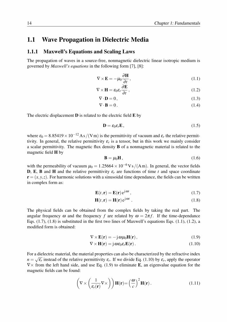
1.1.2 Modes of Translational Invariant WaveguidesA conventional optical waveguide is a dielectric structure that is translational invariant in onedirection and can guide the light along this direction. A mode of a WG is a field distribution thatdoes not change its shape while it propagates. The structure of a dielectric strip WG is shown inFig. 1.1. The refractive index ncore of the WG core needs to be larger than the refractive indexesof the substrate nsub and of the cover material ncover in order to obtain a guided mode in thecore. The direction of the WG is along the z-axis. A mode at frequency ω with a harmonic timedependance ejωt as in Eqs. (1.7) and (1.8) has to satisfy the Maxwell’s equations (1.9), (1.10)and can be written in the form:
Fig. 1.1. Schematic of a strip waveguide. The refractive indices of the waveguide core, the substrate and the coverare denoted as ncore, nsub, and ncover, respectively.
16 Chapter 1: Fundamentals
E(x,y,z) = E(x,y)e− jβ z , (1.14)
H(x,y,z) = H(x,y)e− jβ z . (1.15)
The propagation constant β and the transverse field profile E,H are functions of the fre-quency ω . The dependance of the propagation constant with frequency β (ω) is referred to asthe dispersion relation of the WG mode. For a positive propagation constant, the phase frontspropagates in positive z-direction, for a negative propagation constant in negative z-direction.In many cases, the effective refractive index neff is displayed as a function of frequency insteadof the propagation constant β , and the relation between the two quantities is:
β = neffωc
. (1.16)
Modes with a dominant field component Ex are called (quasi)-transverse electric (TE) modes,whereas modes with a dominant electric field component Ey are called (quasi)-transverse mag-netic (TM) modes. A mode is guided if the effective refractive index exceeds the substrateindex, and for a lower effective index the mode becomes lossy and leaks into the substrate.
150 200 250 3001.5
2.0
2.5
TM
Effe
ctiv
e re
frac
tive
inde
x n ef
f
Frequency f [THz]
TE
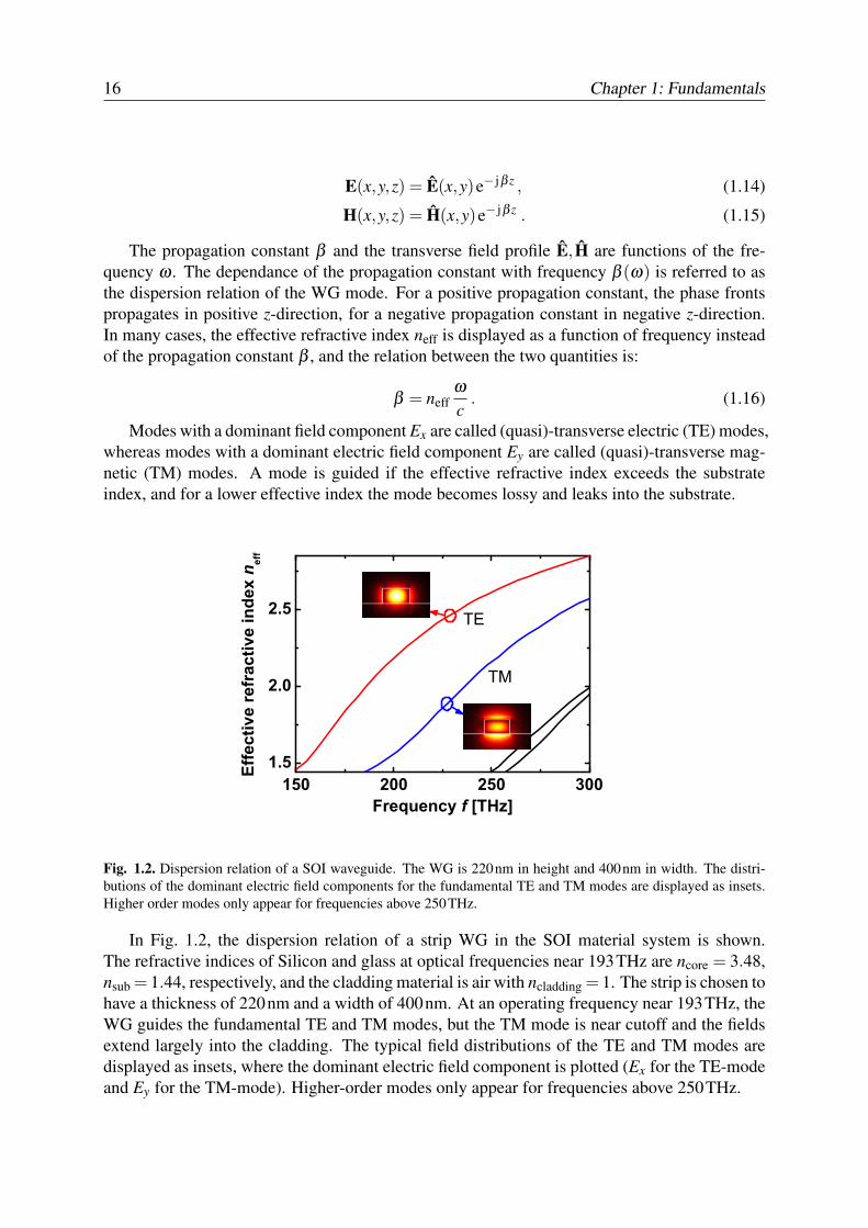
Fig. 1.2. Dispersion relation of a SOI waveguide. The WG is 220nm in height and 400nm in width. The distri-butions of the dominant electric field components for the fundamental TE and TM modes are displayed as insets.Higher order modes only appear for frequencies above 250THz.
In Fig. 1.2, the dispersion relation of a strip WG in the SOI material system is shown.The refractive indices of Silicon and glass at optical frequencies near 193THz are ncore = 3.48,nsub = 1.44, respectively, and the cladding material is air with ncladding = 1. The strip is chosen tohave a thickness of 220nm and a width of 400nm. At an operating frequency near 193THz, theWG guides the fundamental TE and TM modes, but the TM mode is near cutoff and the fieldsextend largely into the cladding. The typical field distributions of the TE and TM modes aredisplayed as insets, where the dominant electric field component is plotted (Ex for the TE-modeand Ey for the TM-mode). Higher-order modes only appear for frequencies above 250THz.
1.2 2D Photonic Crystals 17
For a fixed frequency, the field distribution inside the WG can be represented as a superpo-sition of guided and radiative modes, [10]. For many purposes, it is sufficient to only considerthe guided modes in the expansion. The orthogonality relation for two guided modes Ep,q, Hp,qsubscripted with p and q, respectively, reads [10]:
14
∫∫ (Eq× H∗
p− Hq× E∗p) · ezdA = δp,qPp . (1.17)
The surface integration is performed over a cross-section perpendicular to the propagation di-rection, δp,q is the Kronecker-Delta, and Pp is the cross-section power of mode p. If p = q is setin Eq. 1.17, the power of mode p is determined:
Pp =12
∫∫ℜ
(Ep× H∗
p) · ezdA . (1.18)
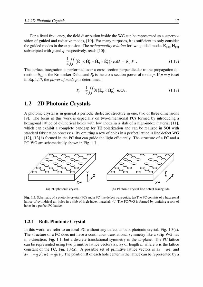
1.2 2D Photonic CrystalsA photonic crystal is in general a periodic dielectric structure in one, two or three dimensions[9]. The focus in this work is especially on two-dimensional PCs formed by introducing ahexagonal lattice of cylindrical holes with low index in a slab of a high-index material [11],which can exhibit a complete bandgap for TE polarization and can be realized in SOI withstandard fabrication processes. By omitting a row of holes in a perfect lattice, a line defect WG[12], [13] is formed in the PC that can guide the light efficiently. The structure of a PC and aPC-WG are schematically shown in Fig. 1.3.
(a) 2D photonic crystal. (b) Photonic crystal line defect waveguide.
Fig. 1.3. Schematic of a photonic crystal (PC) and a PC line defect waveguide. (a) The PC consists of a hexagonallattice of cylindrical air holes in a slab of high-index material. (b) The PC-WG is formed by omitting a row ofholes in a perfect PC lattice.
1.2.1 Bulk Photonic CrystalIn this work, we refer to an ideal PC without any defect as bulk photonic crystal, Fig. 1.3(a).The structure of a PC does not have a continuous translational symmetry like a strip-WG hasin z-direction, Fig. 1.1, but a discrete translational symmetry in the xz-plane. The PC latticecan be represented using two primitive lattice vectors a1, a2 of length a, where a is the latticeconstant of the PC, Fig. 1.4(a). A possible set of primitive lattice vectors is a1 = aez anda2 =−1
2
√3aex + 1
2aez. The position R of each hole center in the lattice can be represented by a
18 Chapter 1: Fundamentals
linear combination of the primitive lattice vectors with integer coefficients l1 and l2, R = l1 a1 +l2 a2. The symmetry of the dielectric structure can thus be represented as εr(r+R) = εr(r). Asthe dielectric structure is symmetric, also the eigenfunctions must exhibit the same symmetry.The eigenfunctions with two-dimensional translational periodicity can be expanded into planewaves e− jG·r having propagation direction G. This expansion corresponds to a two-dimensionalFourier transform of the eigenfunctions. The vectors G of the plane-wave expansion are calledthe reciprocal lattice vectors, and they form the reciprocal lattice, Fig. 1.4(b). As in the directlattice, all vectors in the reciprocal lattice G are a linear combination of two primitive latticevectors b1, b2 with integer coefficients. A possible set of reciprocal lattice vectors is b1 =− 4π√
3aex and b2 = − 2π√
3aex + 2π
a ez. The eigenfunctions of the structure can be classified by awave vector k. Bloch’s theorem states that the eigenfunctions (or modes) can be represented inthe following form [9]:
H(r) = e− jk·r u(r) with u(r) = u(r+R) . (1.19)
The mode field H for a given wave vector k has a periodic part u(r) with periodicity in thelattice vectors R, and has a phase factor e− jk·r. The same law holds for the E-field.
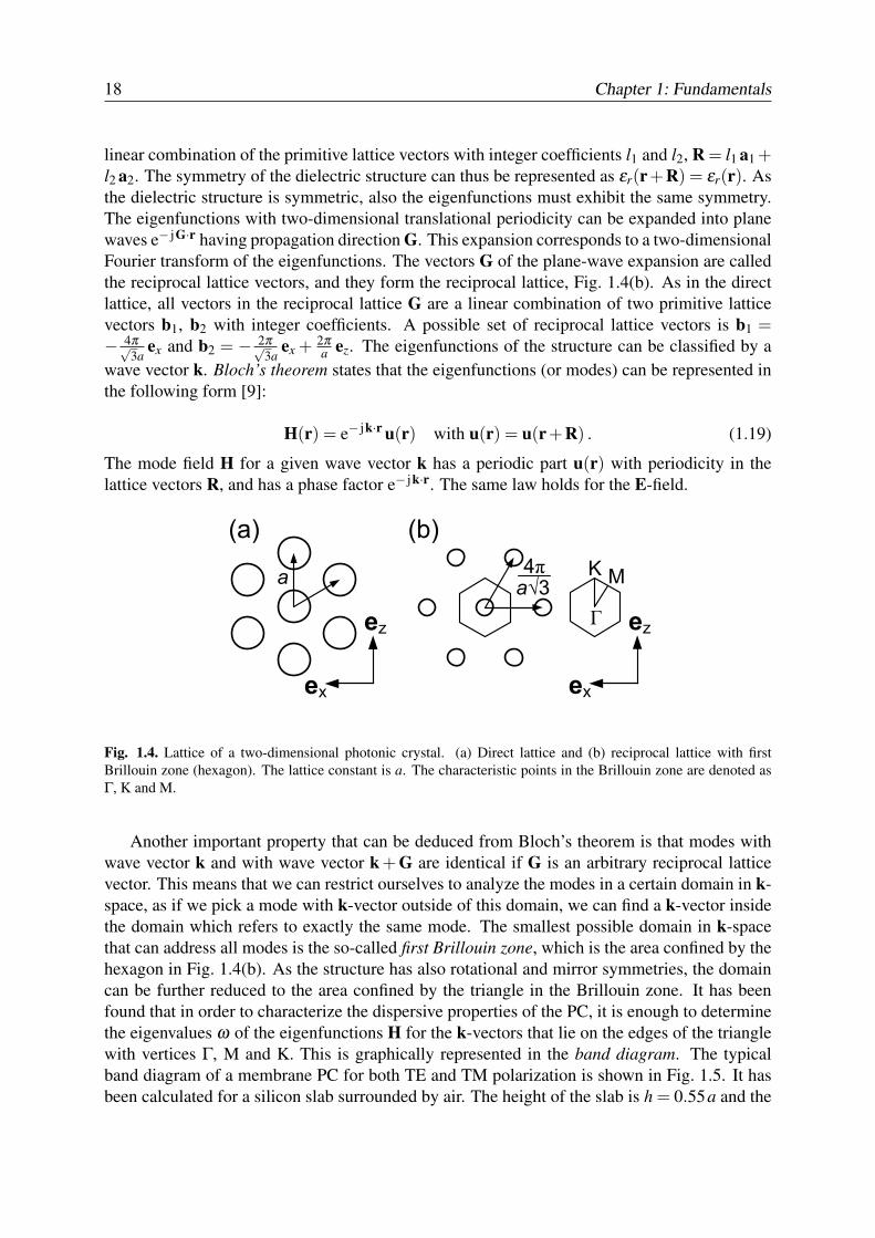
Fig. 1.4. Lattice of a two-dimensional photonic crystal. (a) Direct lattice and (b) reciprocal lattice with firstBrillouin zone (hexagon). The lattice constant is a. The characteristic points in the Brillouin zone are denoted asΓ, K and M.
Another important property that can be deduced from Bloch’s theorem is that modes withwave vector k and with wave vector k + G are identical if G is an arbitrary reciprocal latticevector. This means that we can restrict ourselves to analyze the modes in a certain domain in k-space, as if we pick a mode with k-vector outside of this domain, we can find a k-vector insidethe domain which refers to exactly the same mode. The smallest possible domain in k-spacethat can address all modes is the so-called first Brillouin zone, which is the area confined by thehexagon in Fig. 1.4(b). As the structure has also rotational and mirror symmetries, the domaincan be further reduced to the area confined by the triangle in the Brillouin zone. It has beenfound that in order to characterize the dispersive properties of the PC, it is enough to determinethe eigenvalues ω of the eigenfunctions H for the k-vectors that lie on the edges of the trianglewith vertices Γ, M and K. This is graphically represented in the band diagram. The typicalband diagram of a membrane PC for both TE and TM polarization is shown in Fig. 1.5. It hasbeen calculated for a silicon slab surrounded by air. The height of the slab is h = 0.55a and the
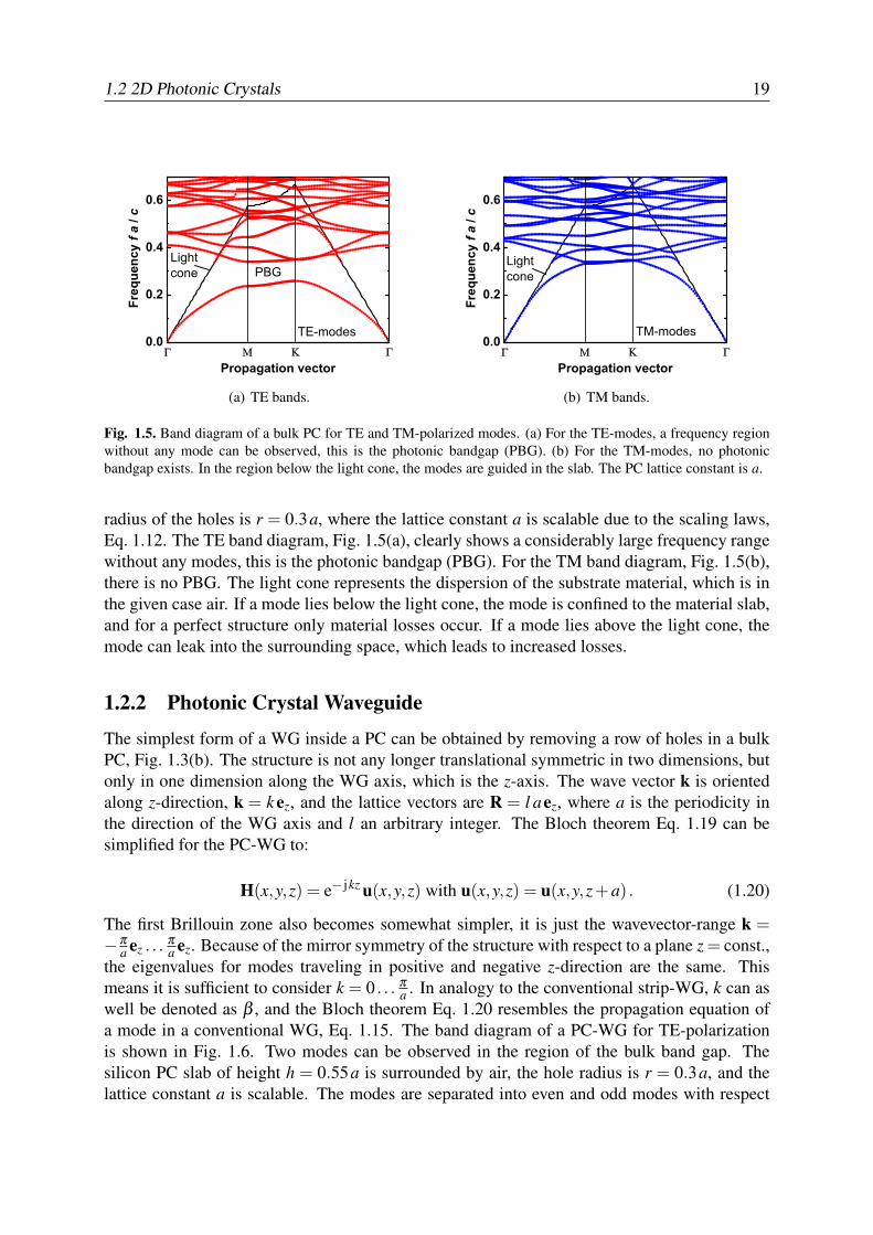
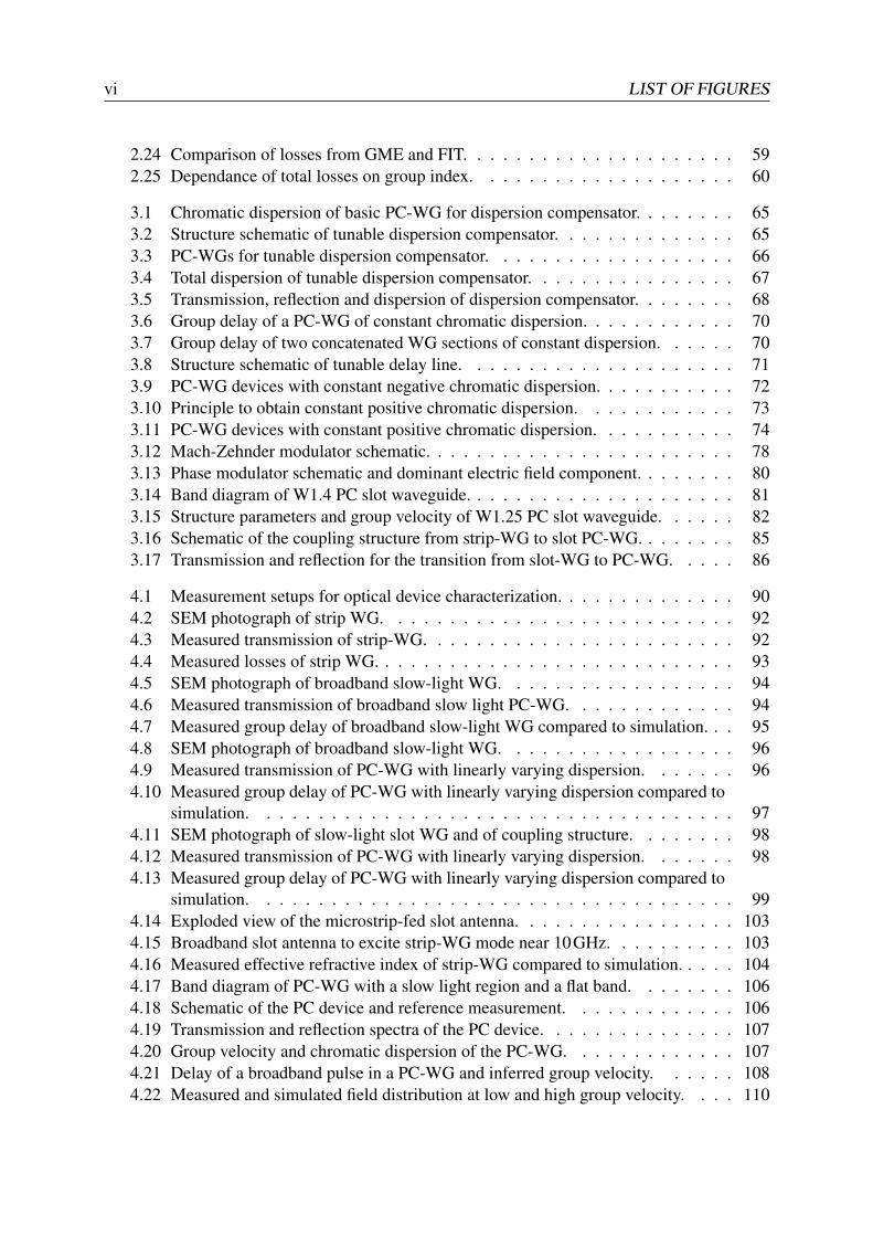
1.2 2D Photonic Crystals 19
0.0
0.2
0.4
0.6
TE-modes
PBG
Freq
uenc
y f a
/ c
Propagation vector
Light cone
(a) TE bands.
0.0
0.2
0.4
0.6
TM-modes
Light cone
Freq
uenc
y f a
/ c
Propagation vector
(b) TM bands.
Fig. 1.5. Band diagram of a bulk PC for TE and TM-polarized modes. (a) For the TE-modes, a frequency regionwithout any mode can be observed, this is the photonic bandgap (PBG). (b) For the TM-modes, no photonicbandgap exists. In the region below the light cone, the modes are guided in the slab. The PC lattice constant is a.
radius of the holes is r = 0.3a, where the lattice constant a is scalable due to the scaling laws,Eq. 1.12. The TE band diagram, Fig. 1.5(a), clearly shows a considerably large frequency rangewithout any modes, this is the photonic bandgap (PBG). For the TM band diagram, Fig. 1.5(b),there is no PBG. The light cone represents the dispersion of the substrate material, which is inthe given case air. If a mode lies below the light cone, the mode is confined to the material slab,and for a perfect structure only material losses occur. If a mode lies above the light cone, themode can leak into the surrounding space, which leads to increased losses.
1.2.2 Photonic Crystal Waveguide
The simplest form of a WG inside a PC can be obtained by removing a row of holes in a bulkPC, Fig. 1.3(b). The structure is not any longer translational symmetric in two dimensions, butonly in one dimension along the WG axis, which is the z-axis. The wave vector k is orientedalong z-direction, k = k ez, and the lattice vectors are R = l aez, where a is the periodicity inthe direction of the WG axis and l an arbitrary integer. The Bloch theorem Eq. 1.19 can besimplified for the PC-WG to:
H(x,y,z) = e− jkz u(x,y,z) with u(x,y,z) = u(x,y,z+a) . (1.20)
The first Brillouin zone also becomes somewhat simpler, it is just the wavevector-range k =−π
a ez . . .πa ez. Because of the mirror symmetry of the structure with respect to a plane z = const.,
the eigenvalues for modes traveling in positive and negative z-direction are the same. Thismeans it is sufficient to consider k = 0 . . . π
a . In analogy to the conventional strip-WG, k can aswell be denoted as β , and the Bloch theorem Eq. 1.20 resembles the propagation equation ofa mode in a conventional WG, Eq. 1.15. The band diagram of a PC-WG for TE-polarizationis shown in Fig. 1.6. Two modes can be observed in the region of the bulk band gap. Thesilicon PC slab of height h = 0.55a is surrounded by air, the hole radius is r = 0.3a, and thelattice constant a is scalable. The modes are separated into even and odd modes with respect

20 Chapter 1: Fundamentals
0.0 0.2 0.4 0.6 0.8 1.00.24
0.26
0.28
0.30
0.32
0.34
0.36
Light line
Freq
uenc
y f a
/ c
Propagation constant k a /
Even modeOdd mode
Fig. 1.6. Band diagram of a line defect PC-WG for the TE modes. Two defect modes appear inside the photonicband gap. The dominant electric field for a typical even and odd mode is shown as insets, and the field of the oddmode resembles the field of a fundamental strip-WG mode.
to a reflection in the yz-plane, which is the vertical plane that bisects the WG, see Fig. 1.3(b).Note that this classification into even and odd modes might be different from what is found inliterature, where the classification is not consistent and even and odd might also refer to (quasi-) TE and TM modes, or even might correspond to our odd and odd to our even modes. Thedistribution of the dominant electric field component Ex for the even and odd mode is shown asinsets, and the field of the odd mode resembles the field of a fundamental strip-WG mode. Thelight cone reduces to the light line, and modes below the light line are confined to the PC slaband have low losses, whereas modes above the light line become leaky. The defect modes of thePC-WG lie within the TE-bandgap of the bulk PC, but for low and high frequencies, the bulkbands appear. As there is no bandgap of the bulk PC for TM-polarization, we restrict ourselvesto TE-operation.
For the modes of a line-defect PC-WG, the same orthogonality relation Eq. (1.17) holds asfor the modes of conventional WGs. This is derived in Appendix A.3.
1.3 Group Velocity and Chromatic Dispersion
The phase fronts of a signal propagating in a strip-WG or a PC-WG travel with the phasevelocity vp, which is inversely proportional to the propagation constant β . The information in asignal is contained in the temporal changes of the signal amplitude and/or phase. In the simplestcase, a logical 1 is represented by a short amplitude pulse, whereas for a logical 0 no pulse ispresent. The pulse centers however do not travel with the phase velocity vp, but with the groupvelocity vg, and the power flow is directly related to the group velocity. As pulses propagatealong a WG, they might gradually change their shape, which is caused by the fact that differentfrequency components of the signal might travel with different group velocities. The change ofthe temporal width of a pulse during propagation can be quantified by the chromatic dispersion
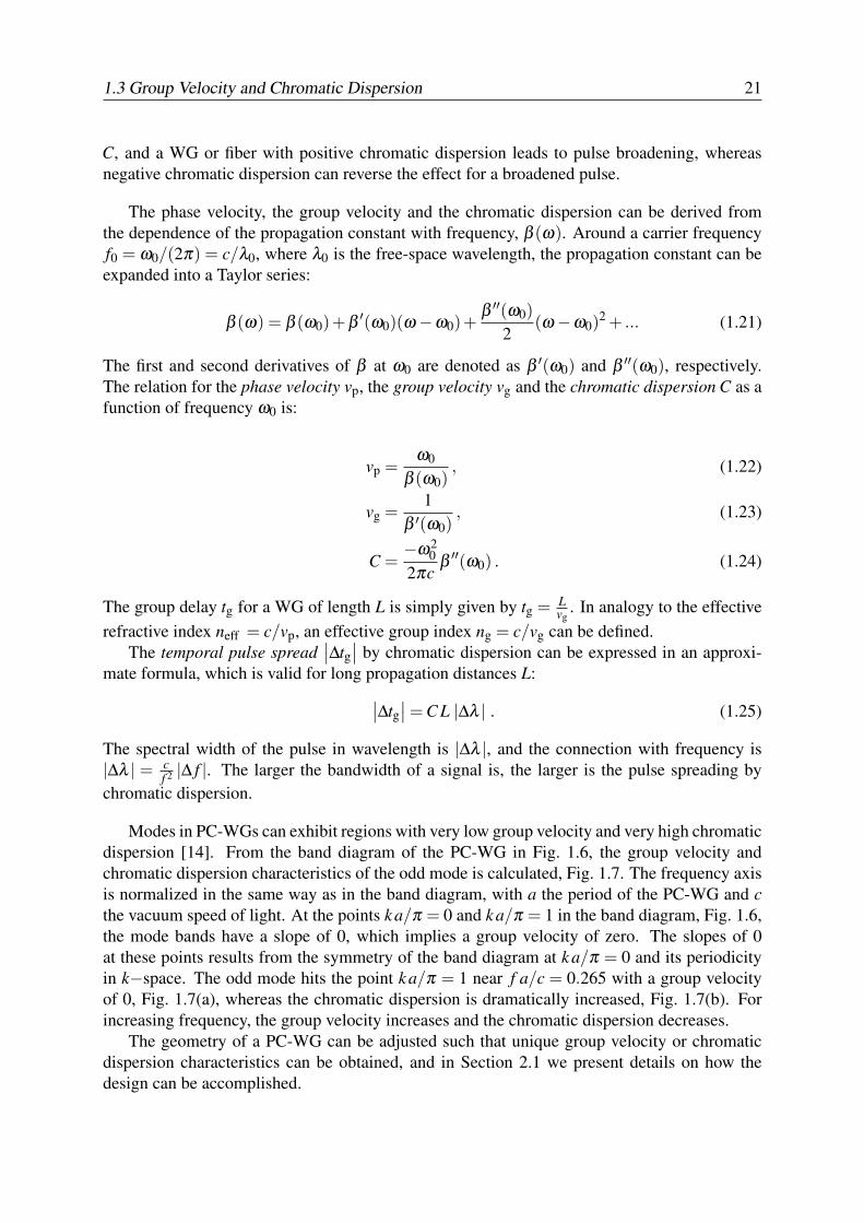
1.3 Group Velocity and Chromatic Dispersion 21
C, and a WG or fiber with positive chromatic dispersion leads to pulse broadening, whereasnegative chromatic dispersion can reverse the effect for a broadened pulse.
The phase velocity, the group velocity and the chromatic dispersion can be derived fromthe dependence of the propagation constant with frequency, β (ω). Around a carrier frequencyf0 = ω0/(2π) = c/λ0, where λ0 is the free-space wavelength, the propagation constant can beexpanded into a Taylor series:
β (ω) = β (ω0)+β ′(ω0)(ω−ω0)+β ′′(ω0)
2(ω−ω0)2 + ... (1.21)
The first and second derivatives of β at ω0 are denoted as β ′(ω0) and β ′′(ω0), respectively.The relation for the phase velocity vp, the group velocity vg and the chromatic dispersion C as afunction of frequency ω0 is:
vp =ω0
β (ω0), (1.22)
vg =1
β ′(ω0), (1.23)
C =−ω2
02πc
β ′′(ω0) . (1.24)
The group delay tg for a WG of length L is simply given by tg = Lvg
. In analogy to the effectiverefractive index neff = c/vp, an effective group index ng = c/vg can be defined.
The temporal pulse spread∣∣∆tg
∣∣ by chromatic dispersion can be expressed in an approxi-mate formula, which is valid for long propagation distances L:
∣∣∆tg∣∣ = C L |∆λ | . (1.25)
The spectral width of the pulse in wavelength is |∆λ |, and the connection with frequency is|∆λ | = c
f 2 |∆ f |. The larger the bandwidth of a signal is, the larger is the pulse spreading bychromatic dispersion.
Modes in PC-WGs can exhibit regions with very low group velocity and very high chromaticdispersion [14]. From the band diagram of the PC-WG in Fig. 1.6, the group velocity andchromatic dispersion characteristics of the odd mode is calculated, Fig. 1.7. The frequency axisis normalized in the same way as in the band diagram, with a the period of the PC-WG and cthe vacuum speed of light. At the points k a/π = 0 and k a/π = 1 in the band diagram, Fig. 1.6,the mode bands have a slope of 0, which implies a group velocity of zero. The slopes of 0at these points results from the symmetry of the band diagram at k a/π = 0 and its periodicityin k−space. The odd mode hits the point k a/π = 1 near f a/c = 0.265 with a group velocityof 0, Fig. 1.7(a), whereas the chromatic dispersion is dramatically increased, Fig. 1.7(b). Forincreasing frequency, the group velocity increases and the chromatic dispersion decreases.
The geometry of a PC-WG can be adjusted such that unique group velocity or chromaticdispersion characteristics can be obtained, and in Section 2.1 we present details on how thedesign can be accomplished.
22 Chapter 1: Fundamentals
0.265 0.270 0.275 0.280 0.285 0.2900.00
0.05
0.10
0.15
0.20
0.25
Gro
up v
eloc
ity v
g / c
Frequency f a / c
(a) Group velocity.
0.265 0.270 0.275 0.280 0.285 0.2900
5
10
15
20
Dis
pers
ion
C [p
s/(m
m n
m)]
Frequency f a / c
(b) Chromatic Dispersion.
Fig. 1.7. Group velocity and chromatic dispersion of a PC-WG. (a) The group velocity is normalized to the vacuumspeed of light c. For (a) and (b), the frequency axis is normalized, where a is the PC period. For frequencies nearthe band edge f a/c = 0.265, the group velocity is very low and the chromatic dispersion very high.
The delaying and strongly dispersive properties of PCs can be used to build small functionaldevices like optical delay lines or dispersion compensators. In Section 3.1 of this work wepresent a tunable chromatic dispersion compensator, and in Section 3.2 a tunable optical delayline.
A second important effect of light propagation at low group velocity is that the interactionbetween light and matter is increased, which enhances nonlinear effects [15] and allows to de-crease the size and to increase the efficiency of nonlinear devices like modulators, switches,wavelength converters or amplifiers. For an electro-optic device, the length to achieve a cer-tain phase shift decreases proportionally with decreasing vg, and the operational power for thesmaller device also decreases. For an all-optical nonlinear device, the Kerr effect dependson the square of the electric field and increases inversely proportional with decreasing groupvelocity, and again at the same time the device length is decreased. Silicon is a centrosym-metric crystal, which means that there exist no χ(2)-effects, like the linear electro-optic effect.However, a χ(2)-effect in silicon can be induced by e. g. straining the crystal [16], or by infil-trating an electro-optic material into a silicon structure, like an electro-optic polymer [17] or achalcogenide [18]. Furthermore, silicon exhibits χ(3)-effects, and stimulated Raman scattering[19], [20] and four-wave-mixing [21] have been demonstrated. In Section 3.3 we present a fastelectro-optical modulator with low operation voltage.
Propagation losses, however, increase with decreasing group velocity, [15], [22], whichmight eventually limit the device performance. We especially address the issue of disorder-induced losses in PCs at low group velocity in Section 2.2 of this work.
1.4 Mode Gaps and Mini-Stop Bands in PC Waveguides
From the band diagram Fig. 1.6 it can be observed that inside the PBG there is a frequencyrange for which no mode can propagate in the WG, this is for frequencies below the cut-offof the odd mode near f a/c = 0.265. This region is called a mode gap [23], and it arises from
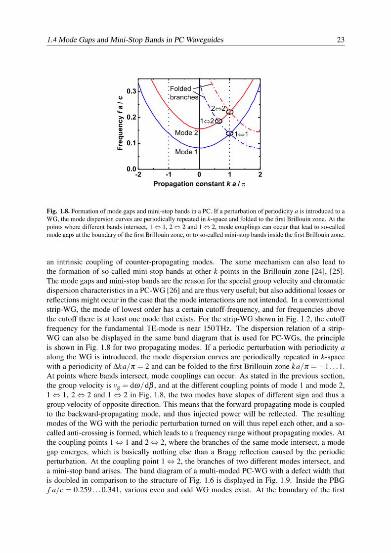
1.4 Mode Gaps and Mini-Stop Bands in PC Waveguides 23
-2 -1 0 1 20.0
0.1
0.2
0.3
1 2
2 2
1 1
Foldedbranches
Mode 2
Mode 1
Freq
uenc
y f a
/ c
Propagation constant k a /
Fig. 1.8. Formation of mode gaps and mini-stop bands in a PC. If a perturbation of periodicity a is introduced to aWG, the mode dispersion curves are periodically repeated in k-space and folded to the first Brillouin zone. At thepoints where different bands intersect, 1 ⇔ 1, 2 ⇔ 2 and 1 ⇔ 2, mode couplings can occur that lead to so-calledmode gaps at the boundary of the first Brillouin zone, or to so-called mini-stop bands inside the first Brillouin zone.
an intrinsic coupling of counter-propagating modes. The same mechanism can also lead tothe formation of so-called mini-stop bands at other k-points in the Brillouin zone [24], [25].The mode gaps and mini-stop bands are the reason for the special group velocity and chromaticdispersion characteristics in a PC-WG [26] and are thus very useful; but also additional losses orreflections might occur in the case that the mode interactions are not intended. In a conventionalstrip-WG, the mode of lowest order has a certain cutoff-frequency, and for frequencies abovethe cutoff there is at least one mode that exists. For the strip-WG shown in Fig. 1.2, the cutofffrequency for the fundamental TE-mode is near 150THz. The dispersion relation of a strip-WG can also be displayed in the same band diagram that is used for PC-WGs, the principleis shown in Fig. 1.8 for two propagating modes. If a periodic perturbation with periodicity aalong the WG is introduced, the mode dispersion curves are periodically repeated in k-spacewith a periodicity of ∆k a/π = 2 and can be folded to the first Brillouin zone k a/π = −1 . . .1.At points where bands intersect, mode couplings can occur. As stated in the previous section,the group velocity is vg = dω/dβ , and at the different coupling points of mode 1 and mode 2,1 ⇔ 1, 2 ⇔ 2 and 1 ⇔ 2 in Fig. 1.8, the two modes have slopes of different sign and thus agroup velocity of opposite direction. This means that the forward-propagating mode is coupledto the backward-propagating mode, and thus injected power will be reflected. The resultingmodes of the WG with the periodic perturbation turned on will thus repel each other, and a so-called anti-crossing is formed, which leads to a frequency range without propagating modes. Atthe coupling points 1 ⇔ 1 and 2 ⇔ 2, where the branches of the same mode intersect, a modegap emerges, which is basically nothing else than a Bragg reflection caused by the periodicperturbation. At the coupling point 1 ⇔ 2, the branches of two different modes intersect, anda mini-stop band arises. The band diagram of a multi-moded PC-WG with a defect width thatis doubled in comparison to the structure of Fig. 1.6 is displayed in Fig. 1.9. Inside the PBGf a/c = 0.259 . . .0.341, various even and odd WG modes exist. At the boundary of the first
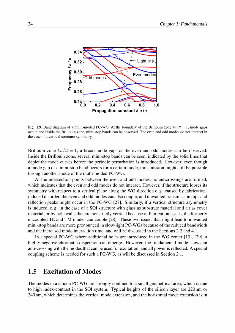
24 Chapter 1: Fundamentals
0.0 0.2 0.4 0.6 0.8 1.00.24
0.26
0.28
0.30
0.32
0.34
Light line
Freq
uenc
y f a
/ c
Propagation constant k a /
Even modesOdd modes
Fig. 1.9. Band diagram of a multi-moded PC-WG. At the boundary of the Brillouin zone ka/π = 1, mode gapsoccur, and inside the Brillouin zone, mini-stop bands can be observed. The even and odd modes do not interact inthe case of a vertical structure symmetry.
Brillouin zone k a/π = 1, a broad mode gap for the even and odd modes can be observed.Inside the Brillouin zone, several mini-stop bands can be seen, indicated by the solid lines thatdepict the mode curves before the periodic perturbation is introduced. However, even thougha mode gap or a mini-stop band occurs for a certain mode, transmission might still be possiblethrough another mode of the multi-moded PC-WG.
At the intersection points between the even and odd modes, no anticrossings are formed,which indicates that the even and odd modes do not interact. However, if the structure looses itssymmetry with respect to a vertical plane along the WG-direction e. g. caused by fabrication-induced disorder, the even and odd modes can also couple, and unwanted transmission dips andreflection peaks might occur in the PC-WG [27]. Similarly, if a vertical structure asymmetryis induced, e. g. in the case of a SOI structure with glass as substrate material and air as covermaterial, or by hole walls that are not strictly vertical because of fabrication issues, the formerlyuncoupled TE and TM modes can couple [28]. These two issues that might lead to unwantedmini-stop bands are more pronounced in slow-light PC-WGs because of the reduced bandwidthand the increased mode interaction time, and will be discussed in the Sections 2.2 and 4.1.
In a special PC-WG where additional holes are introduced in the WG center [13], [29], ahighly negative chromatic dispersion can emerge. However, the fundamental mode shows ananti-crossing with the modes that can be used for excitation, and all power is reflected. A specialcoupling scheme is needed for such a PC-WG, as will be discussed in Section 2.1.
1.5 Excitation of Modes
The modes in a silicon PC-WG are strongly confined to a small geometrical area, which is dueto high index-contrast in the SOI system. Typical heights of the silicon layer are 220nm or340nm, which determines the vertical mode extension, and the horizontal mode extension is in
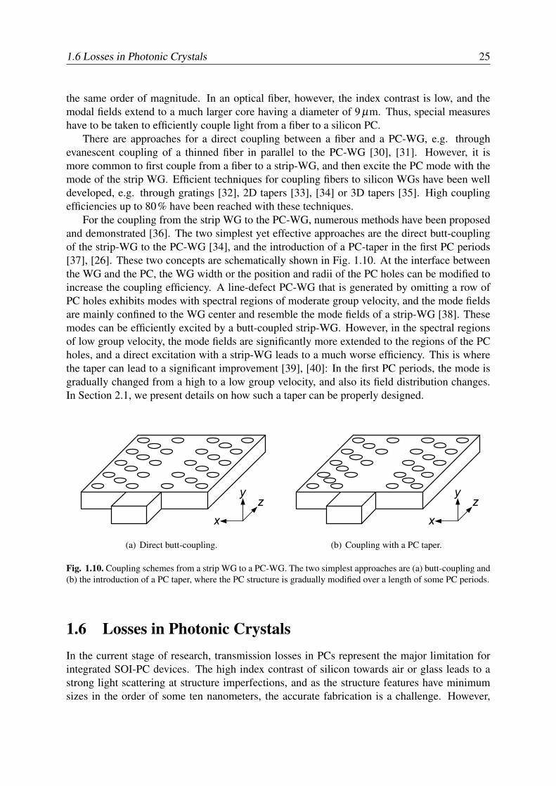
1.6 Losses in Photonic Crystals 25
the same order of magnitude. In an optical fiber, however, the index contrast is low, and themodal fields extend to a much larger core having a diameter of 9 µm. Thus, special measureshave to be taken to efficiently couple light from a fiber to a silicon PC.
There are approaches for a direct coupling between a fiber and a PC-WG, e.g. throughevanescent coupling of a thinned fiber in parallel to the PC-WG [30], [31]. However, it ismore common to first couple from a fiber to a strip-WG, and then excite the PC mode with themode of the strip WG. Efficient techniques for coupling fibers to silicon WGs have been welldeveloped, e.g. through gratings [32], 2D tapers [33], [34] or 3D tapers [35]. High couplingefficiencies up to 80% have been reached with these techniques.
For the coupling from the strip WG to the PC-WG, numerous methods have been proposedand demonstrated [36]. The two simplest yet effective approaches are the direct butt-couplingof the strip-WG to the PC-WG [34], and the introduction of a PC-taper in the first PC periods[37], [26]. These two concepts are schematically shown in Fig. 1.10. At the interface betweenthe WG and the PC, the WG width or the position and radii of the PC holes can be modified toincrease the coupling efficiency. A line-defect PC-WG that is generated by omitting a row ofPC holes exhibits modes with spectral regions of moderate group velocity, and the mode fieldsare mainly confined to the WG center and resemble the mode fields of a strip-WG [38]. Thesemodes can be efficiently excited by a butt-coupled strip-WG. However, in the spectral regionsof low group velocity, the mode fields are significantly more extended to the regions of the PCholes, and a direct excitation with a strip-WG leads to a much worse efficiency. This is wherethe taper can lead to a significant improvement [39], [40]: In the first PC periods, the mode isgradually changed from a high to a low group velocity, and also its field distribution changes.In Section 2.1, we present details on how such a taper can be properly designed.
(a) Direct butt-coupling. (b) Coupling with a PC taper.
Fig. 1.10. Coupling schemes from a strip WG to a PC-WG. The two simplest approaches are (a) butt-coupling and(b) the introduction of a PC taper, where the PC structure is gradually modified over a length of some PC periods.
1.6 Losses in Photonic CrystalsIn the current stage of research, transmission losses in PCs represent the major limitation forintegrated SOI-PC devices. The high index contrast of silicon towards air or glass leads to astrong light scattering at structure imperfections, and as the structure features have minimumsizes in the order of some ten nanometers, the accurate fabrication is a challenge. However,
26 Chapter 1: Fundamentals
in the last years, great improvements in the disorder-induced losses of silicon strip WGs andPC-WGs have been achieved. The losses for a SOI strip WG of width w = 500nm and ofheight h = 220nm are 2.4dB/cm [41] and the losses for a membrane W1 PC-WG with slabheight h = 220nm, hole radii r = 240nm and a lattice constant a = 430nm could be reduced to4.1dB/cm [42]. Further improvements are still to be expected. For comparison, the losses of astandard SMF are 0.15×10⁻⁵ dB/cm. The losses in PC-WGs can be divided into intrinsic andextrinsic losses.
The intrinsic losses are the inherent losses of the WG, which are the linear and nonlinearmaterial losses of silicon, and the leakage losses of the modes out of the slab if the conditionof total internal reflection (TIR) is no longer met. The linear material losses of silicon arenegligible [43]. The important nonlinear losses are two-photon absorption (TPA) [44] and free-carrier absorption (FCA) [45], and TPA can induce FCA [46]. For passive PC devices operatedat low power levels, these nonlinear losses do not play a role either. The condition for TIR in theslab is met if the modes of the PC-WG stay below the light-lines of the substrate and the covermaterial [11]. In that case, there are no leakage losses of an ideal structure [47]. However,as soon as a mode crosses the light line, it can couple to radiative modes in the substrate orthe cover and considerable losses can occur [48], [49]. A mode lying above the light line thusbecomes a leaky mode, which is similar to a leaky mode in a fiber or a strip WG. The light linerepresents the dispersion of a wave that propagates in a homogeneous medium with refractiveindex nll:
kll = nllωc
or ωll =k cnll
. (1.26)
If the substrate and cover materials have different refractive indices, the larger refractive indexneeds to be considered as nll. This is the case as a larger refractive index leads to a light line thatlies lower in the band diagram, and as soon as the lowest light line is exceeded, leakage lossesarise. The higher the background index of a PC-WG is, the smaller is the low-loss frequencyand wavevector range of the WG mode. Therefore it is desirable to choose a low backgroundindex, like e. g. air.
The extrinsic losses are the losses that are caused by non-ideal structures. They includefabrication-induced effects like insufficient hole depth [50], non-vertical sidewalls [28], [50],surface roughness [51], [52], disorder in the hole centers or hole radii [53], [54], and materialinhomogeneities. In a PC-WG, the extrinsic losses can be separated in several contributions,see Fig. 1.11. We can distinguish between out-of-plane losses, in-plane losses and backscatterlosses into the counterpropagating mode, and denote corresponding power loss factors αo, αpand αb, respectively. At the interface between a strip-WG or a homogeneous material to aPC-WG, power can also be diffracted into space. If the PC-WG is operated inside the PBGand a sufficiently large number of holes is placed next to the WG, the in-plane losses αp aresmall compared to αo and αb even in the presence of disorder or roughness, as the PBG ofthe bulk PC is relatively robust towards disorder and a large degree of disorder is needed tospoil the PBG [55], [56]. Currently, the losses in PC devices are mainly caused by imperfectfabrication processes. For line-defect PC-WGs, it is suggested that the transmission losses scalequadratically with the disorder variance σ [57], and that the losses are proportional to at leastthe first power of the group index [58], [59]. The knowledge of this fact is very important foroperation at low group velocities, as it might introduce severe device limitations. In Section 2.2,we study the influence of radial disorder on the characteristics of slow-light PC-WGs.
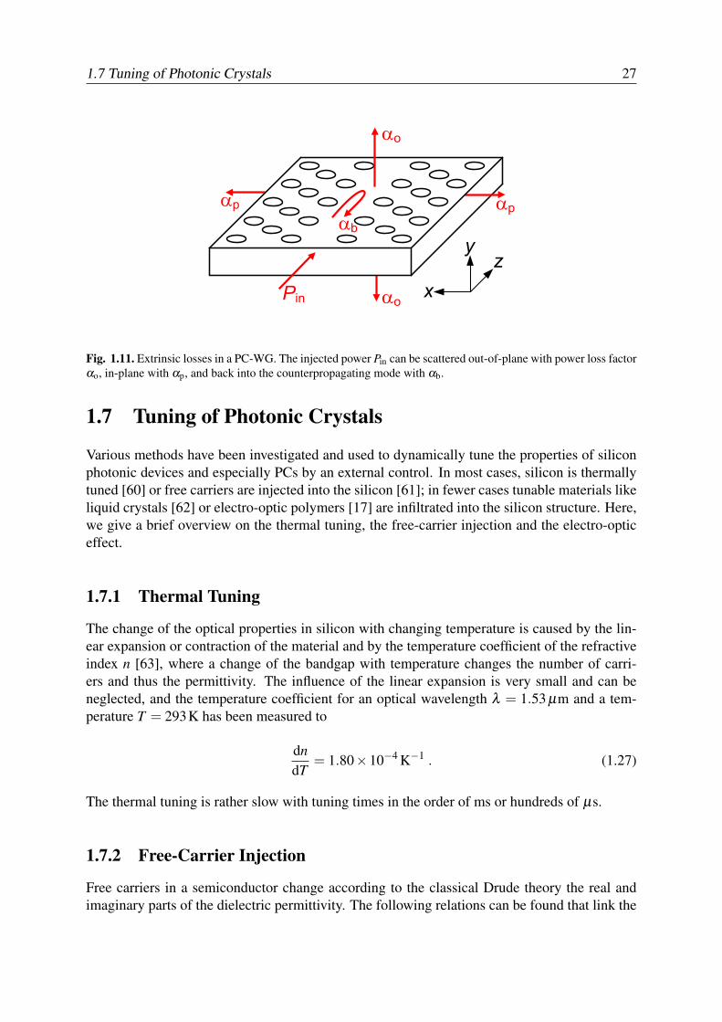
1.7 Tuning of Photonic Crystals 27
Fig. 1.11. Extrinsic losses in a PC-WG. The injected power Pin can be scattered out-of-plane with power loss factorαo, in-plane with αp, and back into the counterpropagating mode with αb.
1.7 Tuning of Photonic Crystals
Various methods have been investigated and used to dynamically tune the properties of siliconphotonic devices and especially PCs by an external control. In most cases, silicon is thermallytuned [60] or free carriers are injected into the silicon [61]; in fewer cases tunable materials likeliquid crystals [62] or electro-optic polymers [17] are infiltrated into the silicon structure. Here,we give a brief overview on the thermal tuning, the free-carrier injection and the electro-opticeffect.
1.7.1 Thermal Tuning
The change of the optical properties in silicon with changing temperature is caused by the lin-ear expansion or contraction of the material and by the temperature coefficient of the refractiveindex n [63], where a change of the bandgap with temperature changes the number of carri-ers and thus the permittivity. The influence of the linear expansion is very small and can beneglected, and the temperature coefficient for an optical wavelength λ = 1.53 µm and a tem-perature T = 293K has been measured to
dndT
= 1.80×10⁻⁴ K−1 . (1.27)
The thermal tuning is rather slow with tuning times in the order of ms or hundreds of µs.
1.7.2 Free-Carrier Injection
Free carriers in a semiconductor change according to the classical Drude theory the real andimaginary parts of the dielectric permittivity. The following relations can be found that link the
28 Chapter 1: Fundamentals
change in refractive index ∆n and the change in absorption ∆α with the change in electron andhole concentrations ∆N and ∆P, respectively [45]:
∆n =− e20 λ 2
8π2c2ε0nSi
(∆Nmn
+∆Pmp
), (1.28)
∆α =e3
0 λ 2
4π2c3ε0nSi
(∆N
m2n µn
+∆P
m2p µp
). (1.29)
The electron charge is e0, the effective masses and mobilities of the electron and holes are mn,mp and µn, µp, respectively, nSi is the refractive index of silicon and λ the free-space wavelengthof the light. Experimentally, the parameters of Eq. (1.28) were determined for silicon at awavelength λ = 1.55 µm and at room temperature, and the exponent of ∆P was empiricallycorrected to 0.8:
∆n =−(
8.8×10⁻²² cm3 ∆N +8.5×10⁻¹⁸ cm2.4 (∆P)0.8)
. (1.30)
The fastest tuning times with free carrier injection are in the order of some tens of ps. The basicspeed limitation comes from the lifetime of the carriers, however the speed can be increased byextracting the free carriers from the WG zone with an electric field.
1.7.3 Electro-Optic EffectThe linear electro-optic or Pockels effect is a nonlinear χ(2)-effect, where an applied electricfield E = (E1,E2,E3) changes the optical refractive index [64]. In terms of the nonlinear polar-ization P = (P1,P2,P3), the Pockels effect can be described as
Pi (ω) = 2∑j, k
χ(2)ijk (ω : 0,ω) Ek (0) Ej (ω) . (1.31)
A polarization Pi (ω) at frequency ω is generated from the interaction of an electric field Ek (0)at frequency zero and an optical field Ej (ω) at frequency ω in the nonlinear medium, and the
interaction strength is quantified with the nonlinear susceptibility χ(2)ijk .
The electric field E can be related to the electric displacement D by the 3×3 impermeabilitymatrix ηij, which is the inverse of the dielectric permeability matrix εrij:
Ei = ∑j
ηijDj . (1.32)
As the dielectric permeability εrij is real and symmetric for an electro-optic material, the sameholds for the impermeability ηij, and the number of coefficients can be reduced η11 = η1,η22 = η2, η33 = η3, η23 = η32 = η4, η13 = η31 = η5, η12 = η21 = η6. The change in theimpermeability ∆ηi = ∆
(1n2
)i
through the electro-optic effect can be expressed by the elec-trooptic coefficients rij and the applied electric field:
∆ηi = ∆(
1n2
)
i= ∑
jrijEj . (1.33)
1.7 Tuning of Photonic Crystals 29
For small changes of the impermeability η , the change of the refractive index n can be approx-imated by:
∆ni ≈−12
n3i rijEj . (1.34)
For electrooptic polymers, the largest electrooptic coefficient is r33, and the direction 3corresponds to the direction along which the poling field was applied to align the electroopticchromophores. Very high electro-optic coefficients up to 170pm/V have been demonstrated ina modulator device operated at λ = 1.55 µm [65].
The electro-optic effect is intrinsically very fast, and the speed limitation comes rather fromexternal effects, e. g. from the electrical feed circuitry.

30 Chapter 1: Fundamentals
Chapter 2
Slow-Light Waveguides
Over the past several years, new methods to dramatically slow down the propagation velocity oflight pulses have been discovered and experimentally proven, which drew a lot of attention andlead to intense research activities in the new field of ‘slow light’. In addition to the basic interestin the physics of light control, there are many new practical applications of slow light, whichinclude an increased light-matter interaction leading to enhanced nonlinearities [15], the directuse of large delays for optical signal processing and storage or for metrology [66], [67], andthe exploitation of a high chromatic dispersion resulting from a strongly varying group velocity[14].
Slow light can be achieved with a multitude of different approaches. In resonant atomicsystems, extremely slow light can be achieved using electromagnetically induced transparency(EIT) [68], [69], [70] however only at low temperature. At room temperature, a similar effect toEIT is exploited called coherent population oscillation (CPO), where slow light could be shownin crystals [71], [72], doped fibers [73] or semiconductors [74], [75], [76]. Furthermore, slowlight could be demonstrated by using stimulated Brillouin scattering (SBS) [77], [78] stimulatedRaman scattering (SRS) [79], [80] or by wavelength conversion and dispersion [81]. So far, allmentioned slow light mechanisms rely on material properties. Moreover, also special materialstructuring can be used to generate slow-light effects. This way, light propagation at low groupvelocity was presented in Bragg fibers [82] or Bragg waveguides [83], in ring resonators orcoupled-resonator optical waveguides (CROWs) [84], [85], [86], and in photonic crystal devices[60], [87], [88].
In this work, we especially study the potential of silicon slow-light photonic crystal wave-guides for application in broadband optical data transmission systems. To this end, we firstneed to gain deeper insight into the properties of slow-light photonic crystal waveguides, andthis insight will later be required to develop more complex slow-light devices and to interpretmeasurement results. This chapter is in particular devoted to two important aspects. First, inSection 2.1 we discuss several useful PC-WG geometries and develop design principles to ob-tain functional PC-WGs with broadband slow light or high chromatic dispersion characteristics,and we present methods for an efficient mode excitation. Second, in Section 2.2 we study thelosses in PC-WGs caused by fabrication imperfections, which represent a major performancelimitation of PC devices. In particular, we examine the influence of radial disorder on broadbandslow-light PC-WGs and we suggest approaches for loss minimization.
31
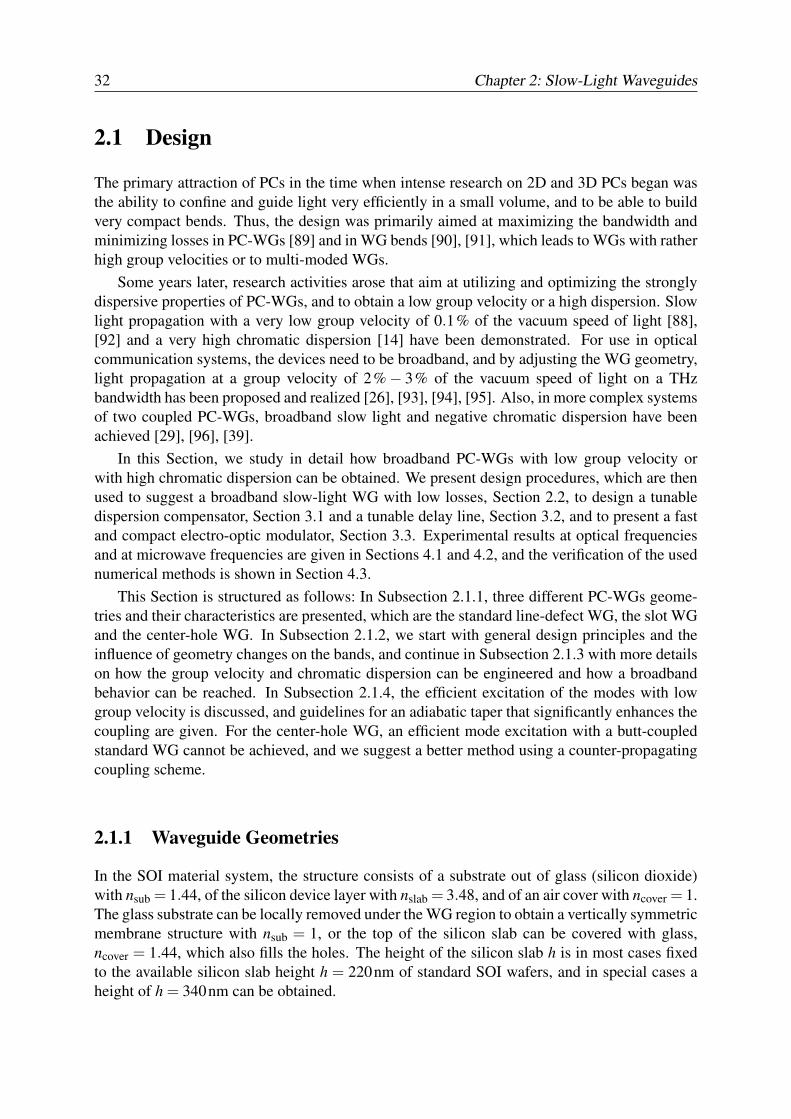
32 Chapter 2: Slow-Light Waveguides
2.1 Design
The primary attraction of PCs in the time when intense research on 2D and 3D PCs began wasthe ability to confine and guide light very efficiently in a small volume, and to be able to buildvery compact bends. Thus, the design was primarily aimed at maximizing the bandwidth andminimizing losses in PC-WGs [89] and in WG bends [90], [91], which leads to WGs with ratherhigh group velocities or to multi-moded WGs.
Some years later, research activities arose that aim at utilizing and optimizing the stronglydispersive properties of PC-WGs, and to obtain a low group velocity or a high dispersion. Slowlight propagation with a very low group velocity of 0.1% of the vacuum speed of light [88],[92] and a very high chromatic dispersion [14] have been demonstrated. For use in opticalcommunication systems, the devices need to be broadband, and by adjusting the WG geometry,light propagation at a group velocity of 2%− 3% of the vacuum speed of light on a THzbandwidth has been proposed and realized [26], [93], [94], [95]. Also, in more complex systemsof two coupled PC-WGs, broadband slow light and negative chromatic dispersion have beenachieved [29], [96], [39].
In this Section, we study in detail how broadband PC-WGs with low group velocity orwith high chromatic dispersion can be obtained. We present design procedures, which are thenused to suggest a broadband slow-light WG with low losses, Section 2.2, to design a tunabledispersion compensator, Section 3.1 and a tunable delay line, Section 3.2, and to present a fastand compact electro-optic modulator, Section 3.3. Experimental results at optical frequenciesand at microwave frequencies are given in Sections 4.1 and 4.2, and the verification of the usednumerical methods is shown in Section 4.3.
This Section is structured as follows: In Subsection 2.1.1, three different PC-WGs geome-tries and their characteristics are presented, which are the standard line-defect WG, the slot WGand the center-hole WG. In Subsection 2.1.2, we start with general design principles and theinfluence of geometry changes on the bands, and continue in Subsection 2.1.3 with more detailson how the group velocity and chromatic dispersion can be engineered and how a broadbandbehavior can be reached. In Subsection 2.1.4, the efficient excitation of the modes with lowgroup velocity is discussed, and guidelines for an adiabatic taper that significantly enhances thecoupling are given. For the center-hole WG, an efficient mode excitation with a butt-coupledstandard WG cannot be achieved, and we suggest a better method using a counter-propagatingcoupling scheme.
2.1.1 Waveguide Geometries
In the SOI material system, the structure consists of a substrate out of glass (silicon dioxide)with nsub = 1.44, of the silicon device layer with nslab = 3.48, and of an air cover with ncover = 1.The glass substrate can be locally removed under the WG region to obtain a vertically symmetricmembrane structure with nsub = 1, or the top of the silicon slab can be covered with glass,ncover = 1.44, which also fills the holes. The height of the silicon slab h is in most cases fixedto the available silicon slab height h = 220nm of standard SOI wafers, and in special cases aheight of h = 340nm can be obtained.
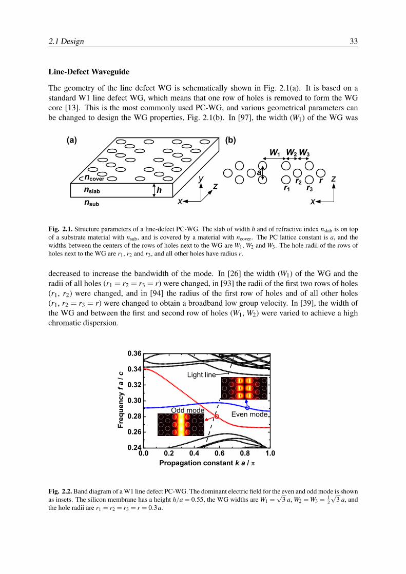
2.1 Design 33
Line-Defect Waveguide
The geometry of the line defect WG is schematically shown in Fig. 2.1(a). It is based on astandard W1 line defect WG, which means that one row of holes is removed to form the WGcore [13]. This is the most commonly used PC-WG, and various geometrical parameters canbe changed to design the WG properties, Fig. 2.1(b). In [97], the width (W1) of the WG was
Fig. 2.1. Structure parameters of a line-defect PC-WG. The slab of width h and of refractive index nslab is on topof a substrate material with nsub, and is covered by a material with ncover. The PC lattice constant is a, and thewidths between the centers of the rows of holes next to the WG are W1, W2 and W3. The hole radii of the rows ofholes next to the WG are r1, r2 and r3, and all other holes have radius r.
decreased to increase the bandwidth of the mode. In [26] the width (W1) of the WG and theradii of all holes (r1 = r2 = r3 = r) were changed, in [93] the radii of the first two rows of holes(r1, r2) were changed, and in [94] the radius of the first row of holes and of all other holes(r1, r2 = r3 = r) were changed to obtain a broadband low group velocity. In [39], the width ofthe WG and between the first and second row of holes (W1, W2) were varied to achieve a highchromatic dispersion.
0.0 0.2 0.4 0.6 0.8 1.00.24
0.26
0.28
0.30
0.32
0.34
0.36
Light line
Freq
uenc
y f a
/ c
Propagation constant k a /
Even modeOdd mode
Fig. 2.2. Band diagram of a W1 line defect PC-WG. The dominant electric field for the even and odd mode is shownas insets. The silicon membrane has a height h/a = 0.55, the WG widths are W1 =
√3 a, W2 = W3 = 1
2
√3 a, and
the hole radii are r1 = r2 = r3 = r = 0.3a.
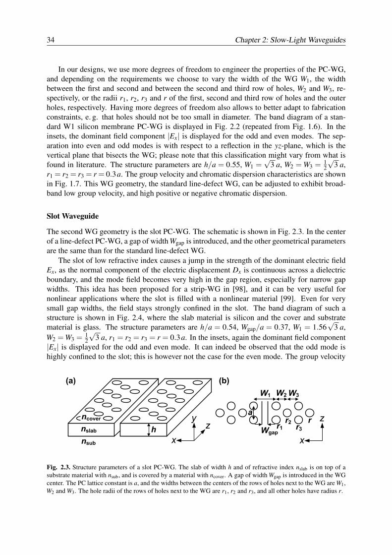
34 Chapter 2: Slow-Light Waveguides
In our designs, we use more degrees of freedom to engineer the properties of the PC-WG,and depending on the requirements we choose to vary the width of the WG W1, the widthbetween the first and second and between the second and third row of holes, W2 and W3, re-spectively, or the radii r1, r2, r3 and r of the first, second and third row of holes and the outerholes, respectively. Having more degrees of freedom also allows to better adapt to fabricationconstraints, e. g. that holes should not be too small in diameter. The band diagram of a stan-dard W1 silicon membrane PC-WG is displayed in Fig. 2.2 (repeated from Fig. 1.6). In theinsets, the dominant field component |Ex| is displayed for the odd and even modes. The sep-aration into even and odd modes is with respect to a reflection in the yz-plane, which is thevertical plane that bisects the WG; please note that this classification might vary from what isfound in literature. The structure parameters are h/a = 0.55, W1 =
√3 a, W2 = W3 = 1
2
√3 a,
r1 = r2 = r3 = r = 0.3a. The group velocity and chromatic dispersion characteristics are shownin Fig. 1.7. This WG geometry, the standard line-defect WG, can be adjusted to exhibit broad-band low group velocity, and high positive or negative chromatic dispersion.
Slot Waveguide
The second WG geometry is the slot PC-WG. The schematic is shown in Fig. 2.3. In the centerof a line-defect PC-WG, a gap of width Wgap is introduced, and the other geometrical parametersare the same than for the standard line-defect WG.
The slot of low refractive index causes a jump in the strength of the dominant electric fieldEx, as the normal component of the electric displacement Dx is continuous across a dielectricboundary, and the mode field becomes very high in the gap region, especially for narrow gapwidths. This idea has been proposed for a strip-WG in [98], and it can be very useful fornonlinear applications where the slot is filled with a nonlinear material [99]. Even for verysmall gap widths, the field stays strongly confined in the slot. The band diagram of such astructure is shown in Fig. 2.4, where the slab material is silicon and the cover and substratematerial is glass. The structure parameters are h/a = 0.54, Wgap/a = 0.37, W1 = 1.56
√3 a,
W2 = W3 = 12
√3 a, r1 = r2 = r3 = r = 0.3a. In the insets, again the dominant field component
|Ex| is displayed for the odd and even mode. It can indeed be observed that the odd mode ishighly confined to the slot; this is however not the case for the even mode. The group velocity
Fig. 2.3. Structure parameters of a slot PC-WG. The slab of width h and of refractive index nslab is on top of asubstrate material with nsub, and is covered by a material with ncover. A gap of width Wgap is introduced in the WGcenter. The PC lattice constant is a, and the widths between the centers of the rows of holes next to the WG are W1,W2 and W3. The hole radii of the rows of holes next to the WG are r1, r2 and r3, and all other holes have radius r.
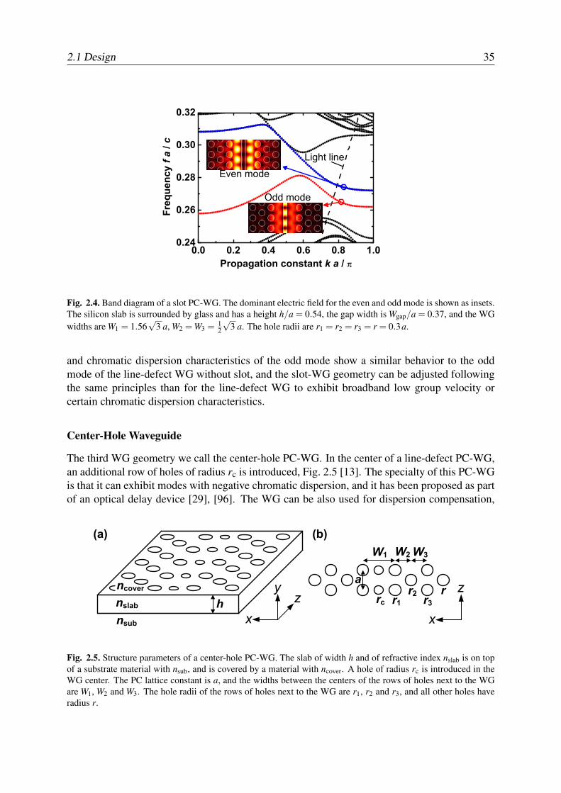
2.1 Design 35
0.0 0.2 0.4 0.6 0.8 1.00.24
0.26
0.28
0.30
0.32
Light line
Freq
uenc
y f a
/ c
Propagation constant k a /
Even mode
Odd mode
Fig. 2.4. Band diagram of a slot PC-WG. The dominant electric field for the even and odd mode is shown as insets.The silicon slab is surrounded by glass and has a height h/a = 0.54, the gap width is Wgap/a = 0.37, and the WGwidths are W1 = 1.56
√3 a, W2 = W3 = 1
2
√3 a. The hole radii are r1 = r2 = r3 = r = 0.3a.
and chromatic dispersion characteristics of the odd mode show a similar behavior to the oddmode of the line-defect WG without slot, and the slot-WG geometry can be adjusted followingthe same principles than for the line-defect WG to exhibit broadband low group velocity orcertain chromatic dispersion characteristics.
Center-Hole Waveguide
The third WG geometry we call the center-hole PC-WG. In the center of a line-defect PC-WG,an additional row of holes of radius rc is introduced, Fig. 2.5 [13]. The specialty of this PC-WGis that it can exhibit modes with negative chromatic dispersion, and it has been proposed as partof an optical delay device [29], [96]. The WG can be also used for dispersion compensation,
Fig. 2.5. Structure parameters of a center-hole PC-WG. The slab of width h and of refractive index nslab is on topof a substrate material with nsub, and is covered by a material with ncover. A hole of radius rc is introduced in theWG center. The PC lattice constant is a, and the widths between the centers of the rows of holes next to the WGare W1, W2 and W3. The hole radii of the rows of holes next to the WG are r1, r2 and r3, and all other holes haveradius r.

36 Chapter 2: Slow-Light Waveguides
0.5 0.6 0.7 0.8 0.9 1.00.28
0.30
0.32
0.34Light line
Freq
uenc
y f a
/ c
Propagation constant k a /
Fig. 2.6. Band diagram of a center-hole PC-WG. The dominant electric field for two odd modes is shown as insets.The slab with nslab = 3.04 is surrounded by air and has a height h/a = 0.6, the other parameters are W1 = 0.9
√3 a,
W2 = 12
√3 a, W3 = 0.87 1
2
√3 a, rc = 0.23a, r1 = r3 = r = 0.3a and r2 = 0.329a.
and a very high negative chromatic dispersion can be achieved. The band diagram of a center-hole WG is shown in Fig. 2.6, and only the odd modes are displayed. The membrane structuresurrounded by air has a refractive index nsub = 3.04, and the structure parameters are h/a = 0.6,W1 = 0.9
√3 a, W2 = 1
2
√3 a, W3 = 0.87 1
2
√3 a, rc = 0.23a, r1 = r3 = r = 0.3a and r2 = 0.329a.
The mode with negative chromatic dispersion is the lower band near the normalized frequencyf a/c = 0.3. The distribution of the dominant field component |Ex| for the lower and the higherband are very similar, and the field is high in the region of the center hole, again because of thecontinuity in the Dx-component leading to an enhancement in the Ex-component in the materialwith low refractive index. The mode can be designed such that a broadband negative chromaticdispersion can be obtained. However, we find that the mode cannot be easily excited by astandard line-defect PC-WG or a strip-WG, whereas this is possible for the higher order mode.This seems peculiar as the mode profiles of the lower and higher mode are very similar. Thisissue will be discussed in more detail in Subsection 2.1.4, and a special excitation scheme issuggested. Because of the complexity of the mode excitation and of a high sensitivity of themode behavior on structure changes, the center-hole WG will be discussed only briefly in thiswork.
2.1.2 Design PrinciplesIn order to design a PC-WG with certain dispersive characteristics, it must first be studied howa change of the structural parameters affects the shape of the mode in the band diagram. Inthe following, the geometrical parameters W1, W2, W3 and r1, r2, r3 of a standard W1-linedefect WG will be varied, and the change in the band diagram is observed, Fig. 2.7(a)-(d). Thechanges are very similar for the line-defect WG and the gap WG; thus we mainly concentrateon the line-defect WG here. The center-hole WG will not be treated in detail. The parametersthat change the WG geometry near the core have a larger effect on the mode characteristics
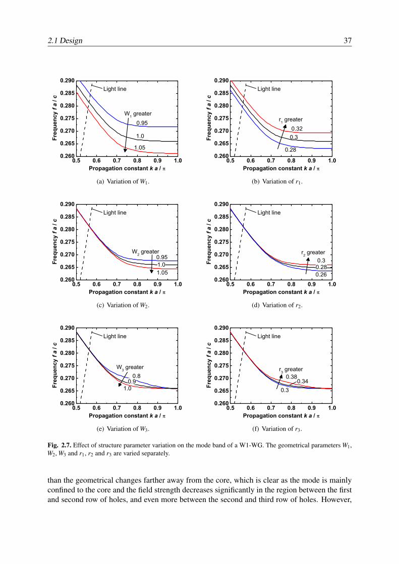
2.1 Design 37
0.5 0.6 0.7 0.8 0.9 1.00.260
0.265
0.270
0.275
0.280
0.285
0.290
1.05
1.0
0.95
Light line
Freq
uenc
y f a
/ c
Propagation constant k a /
W1 greater
(a) Variation of W1.
0.5 0.6 0.7 0.8 0.9 1.00.260
0.265
0.270
0.275
0.280
0.285
0.290
0.320.3
0.28
Light line
Freq
uenc
y f a
/ c
Propagation constant k a /
r1 greater
(b) Variation of r1.
0.5 0.6 0.7 0.8 0.9 1.00.260
0.265
0.270
0.275
0.280
0.285
0.290
1.051.00.95
Light line
Freq
uenc
y f a
/ c
Propagation constant k a /
W2 greater
(c) Variation of W2.
0.5 0.6 0.7 0.8 0.9 1.00.260
0.265
0.270
0.275
0.280
0.285
0.290
0.30.280.26
Light line
Freq
uenc
y f a
/ c
Propagation constant k a /
r2 greater
(d) Variation of r2.
0.5 0.6 0.7 0.8 0.9 1.00.260
0.265
0.270
0.275
0.280
0.285
0.290
1.00.9
0.8
Light line
Freq
uenc
y f a
/ c
Propagation constant k a /
W3 greater
(e) Variation of W3.
0.5 0.6 0.7 0.8 0.9 1.00.260
0.265
0.270
0.275
0.280
0.285
0.290
0.380.34
0.3
Light line
Freq
uenc
y f a
/ c
Propagation constant k a /
r3 greater
(f) Variation of r3.
Fig. 2.7. Effect of structure parameter variation on the mode band of a W1-WG. The geometrical parameters W1,W2, W3 and r1, r2 and r3 are varied separately.
than the geometrical changes farther away from the core, which is clear as the mode is mainlyconfined to the core and the field strength decreases significantly in the region between the firstand second row of holes, and even more between the second and third row of holes. However,
38 Chapter 2: Slow-Light Waveguides
as the group velocity decreases, which happens as the band approaches the edge of the firstBrillouin zone k a/π = 1, the fields extend more into the patterned PC region. The geometrychanges farther away from the core affect the band shape most strongly in the region of lowgroup velocity.
A change in the width between holes Wi , i = 1...3, or in the corresponding hole radius rihas a similar effect on the band deformation, which means that a particular characteristic canbe reached by changing Wi, or ri, or a combination of both. This allows to also take fabricationconstraints into account, e. g. if a certain hole radius would become too small to be fabricatedaccurately, the design can be improved by increasing the hole radius and at the same timeincreasing the corresponding width between holes.
For the band diagrams shown in Fig. 2.7(a)-(d) and in Figs. 2.2-2.6, the mode band of in-terest below the light line is monotonously decreasing or increasing with propagation constant.For certain structure parameters, however, the band might become non-monotonous, which re-sults in spectral ranges with two possible propagation constants at one frequency. This leadsto a mode splitting into two branches at the k-point where the band slope is zero, as in the tworegions the group velocity is of opposite sign (because of opposite signs of the band slope),where one of the mode branches cannot be easily excited. Thus, we try to avoid such bistablebands.
The highest refractive index of the background, nsub or ncover, determines the position of thelight line, and decreasing the refractive index of the background moves up the light line in theband diagram, Eq. (1.26). A mode exhibits low intrinsic losses in the region below the light line,which in the band diagram is the wavevector-range between the intersection point of the modewith the light line and the edge of the first Brillouin zone k a/π = 1. To increase this range, alow background index can be chosen, and the membrane structure with ncover = nsub = 1 wouldbe the best choice. However, a free-standing membrane structure might be more fragile andadditional fabrication steps are needed to remove the substrate. For certain applications, even ahigher background index must be accepted, e. g. if the WG is covered with a nonlinear polymerthe background index increases to npoly ≈ 1.6.
Another possibility to increase the range below the light line is to move the mode down inthe band diagram, which can be achieved by increasing the width W1. However, if W1 is madetoo large, the mode might overlap with bulk PC modes appearing at low frequencies, and theWG might also become multi-moded, which is not desirable for applications where the groupvelocity or chromatic dispersion are the important characteristics. The disorder-induced lossesof a PC-WG also decrease in general with increasing W1. This can be intuitively understood,as for a high WG width, the PC holes having fabrication-induced disorder or roughness aregeometrically farther away from the WG core region with high mode fields. The extrinsic lossmechanisms will be discussed in more detail in Section 2.2.
A third possibility to move the mode down in the band diagram is to choose a larger siliconslab height h; however the standard silicon wafer height is h = 220nm and other heights arerarely available.
The period a of the PC acts in the design process as a scaling parameter which shifts theoperating wavelength to the desired value near λ = 1.55 µm. This is the case because of thescaling law of Maxwell’s equations Eq. (1.12); however for a constant slab height,.the wave-length scales only approximately linearly with the lattice constant.
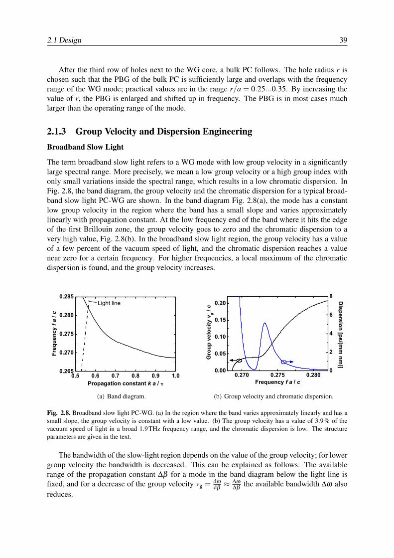
2.1 Design 39
After the third row of holes next to the WG core, a bulk PC follows. The hole radius r ischosen such that the PBG of the bulk PC is sufficiently large and overlaps with the frequencyrange of the WG mode; practical values are in the range r/a = 0.25...0.35. By increasing thevalue of r, the PBG is enlarged and shifted up in frequency. The PBG is in most cases muchlarger than the operating range of the mode.
2.1.3 Group Velocity and Dispersion EngineeringBroadband Slow Light
The term broadband slow light refers to a WG mode with low group velocity in a significantlylarge spectral range. More precisely, we mean a low group velocity or a high group index withonly small variations inside the spectral range, which results in a low chromatic dispersion. InFig. 2.8, the band diagram, the group velocity and the chromatic dispersion for a typical broad-band slow light PC-WG are shown. In the band diagram Fig. 2.8(a), the mode has a constantlow group velocity in the region where the band has a small slope and varies approximatelylinearly with propagation constant. At the low frequency end of the band where it hits the edgeof the first Brillouin zone, the group velocity goes to zero and the chromatic dispersion to avery high value, Fig. 2.8(b). In the broadband slow light region, the group velocity has a valueof a few percent of the vacuum speed of light, and the chromatic dispersion reaches a valuenear zero for a certain frequency. For higher frequencies, a local maximum of the chromaticdispersion is found, and the group velocity increases.
0.5 0.6 0.7 0.8 0.9 1.00.265
0.270
0.275
0.280
0.285Light line
Freq
uenc
y f a
/ c
Propagation constant k a /
(a) Band diagram.
0.270 0.275 0.2800.00
0.05
0.10
0.15
0.20
0
2
4
6
8
Gro
up v
eloc
ity v
g / c
Frequency f a / c
Dispersion [ps/(m
m nm
)]
(b) Group velocity and chromatic dispersion.
Fig. 2.8. Broadband slow light PC-WG. (a) In the region where the band varies approximately linearly and has asmall slope, the group velocity is constant with a low value. (b) The group velocity has a value of 3.9% of thevacuum speed of light in a broad 1.9THz frequency range, and the chromatic dispersion is low. The structureparameters are given in the text.
The bandwidth of the slow-light region depends on the value of the group velocity; for lowergroup velocity the bandwidth is decreased. This can be explained as follows: The availablerange of the propagation constant ∆β for a mode in the band diagram below the light line isfixed, and for a decrease of the group velocity vg = dω
dβ ≈ ∆ω∆β the available bandwidth ∆ω also
reduces.
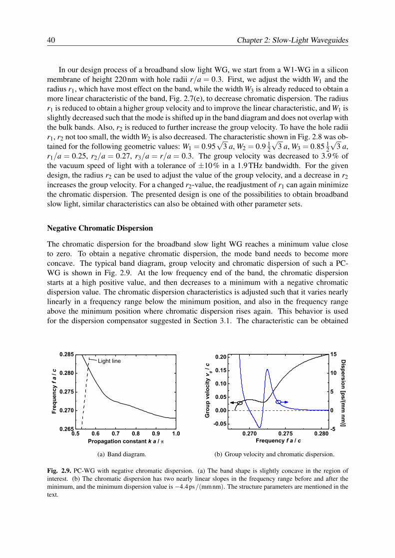
40 Chapter 2: Slow-Light Waveguides
In our design process of a broadband slow light WG, we start from a W1-WG in a siliconmembrane of height 220nm with hole radii r/a = 0.3. First, we adjust the width W1 and theradius r1, which have most effect on the band, while the width W3 is already reduced to obtain amore linear characteristic of the band, Fig. 2.7(e), to decrease chromatic dispersion. The radiusr1 is reduced to obtain a higher group velocity and to improve the linear characteristic, and W1 isslightly decreased such that the mode is shifted up in the band diagram and does not overlap withthe bulk bands. Also, r2 is reduced to further increase the group velocity. To have the hole radiir1, r2 not too small, the width W2 is also decreased. The characteristic shown in Fig. 2.8 was ob-tained for the following geometric values: W1 = 0.95
√3 a, W2 = 0.9 1
2
√3 a, W3 = 0.85 1
2
√3 a,
r1/a = 0.25, r2/a = 0.27, r3/a = r/a = 0.3. The group velocity was decreased to 3.9% ofthe vacuum speed of light with a tolerance of ±10% in a 1.9THz bandwidth. For the givendesign, the radius r2 can be used to adjust the value of the group velocity, and a decrease in r2increases the group velocity. For a changed r2-value, the readjustment of r1 can again minimizethe chromatic dispersion. The presented design is one of the possibilities to obtain broadbandslow light, similar characteristics can also be obtained with other parameter sets.
Negative Chromatic Dispersion
The chromatic dispersion for the broadband slow light WG reaches a minimum value closeto zero. To obtain a negative chromatic dispersion, the mode band needs to become moreconcave. The typical band diagram, group velocity and chromatic dispersion of such a PC-WG is shown in Fig. 2.9. At the low frequency end of the band, the chromatic dispersionstarts at a high positive value, and then decreases to a minimum with a negative chromaticdispersion value. The chromatic dispersion characteristics is adjusted such that it varies nearlylinearly in a frequency range below the minimum position, and also in the frequency rangeabove the minimum position where chromatic dispersion rises again. This behavior is usedfor the dispersion compensator suggested in Section 3.1. The characteristic can be obtained
0.5 0.6 0.7 0.8 0.9 1.00.265
0.270
0.275
0.280
0.285Light line
Freq
uenc
y f a
/ c
Propagation constant k a /
(a) Band diagram.
0.270 0.275 0.280-0.05
0.00
0.05
0.10
0.15
0.20
-5
0
5
10
15
Gro
up v
eloc
ity v
g / c
Frequency f a / c
Dispersion [ps/(m
m nm
)]
(b) Group velocity and chromatic dispersion.
Fig. 2.9. PC-WG with negative chromatic dispersion. (a) The band shape is slightly concave in the region ofinterest. (b) The chromatic dispersion has two nearly linear slopes in the frequency range before and after theminimum, and the minimum dispersion value is −4.4ps/(mmnm). The structure parameters are mentioned in thetext.
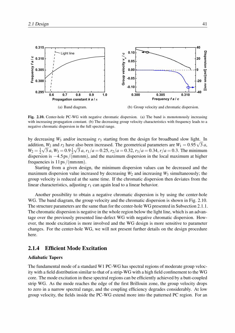
2.1 Design 41
0.6 0.7 0.8 0.9 1.00.295
0.300
0.305
0.310
0.315Light line
Freq
uenc
y f a
/ c
Propagation constant k a /
(a) Band diagram.
0.300 0.305 0.310
-0.10
-0.05
0.00
0.05
0.10
-40
-20
0
20
40
Gro
up v
eloc
ity v
g / c
Frequency f a / c
Dispersion [ps/(m
m nm
)]
(b) Group velocity and chromatic dispersion.
Fig. 2.10. Center-hole PC-WG with negative chromatic dispersion. (a) The band is monotonously increasingwith increasing propagation constant. (b) The decreasing group velocity characteristics with frequency leads to anegative chromatic dispersion in the full spectral range.
by decreasing W3 and/or increasing r3 starting from the design for broadband slow light. Inaddition, W2 and r2 have also been increased. The geometrical parameters are W1 = 0.95
√3 a,
W2 = 12
√3 a, W3 = 0.9 1
2
√3 a, r1/a = 0.25, r2/a = 0.32, r3/a = 0.34, r/a = 0.3. The minimum
dispersion is −4.5ps/(mmnm), and the maximum dispersion in the local maximum at higherfrequencies is 11ps/(mmnm).
Starting from a given design, the minimum dispersion values can be decreased and themaximum dispersion value increased by decreasing W2 and increasing W3 simultaneously; thegroup velocity is reduced at the same time. If the chromatic dispersion then deviates from thelinear characteristics, adjusting r1 can again lead to a linear behavior.
Another possibility to obtain a negative chromatic dispersion is by using the center-holeWG. The band diagram, the group velocity and the chromatic dispersion is shown in Fig. 2.10.The structure parameters are the same than for the center-hole WG presented in Subsection 2.1.1.The chromatic dispersion is negative in the whole region below the light line, which is an advan-tage over the previously presented line-defect WG with negative chromatic dispersion. How-ever, the mode excitation is more involved and the WG design is more sensitive to parameterchanges. For the center-hole WG, we will not present further details on the design procedurehere.
2.1.4 Efficient Mode ExcitationAdiabatic Tapers
The fundamental mode of a standard W1 PC-WG has spectral regions of moderate group veloc-ity with a field distribution similar to that of a strip-WG with a high field confinement to the WGcore. The mode excitation in these spectral regions can be efficiently achieved by a butt-coupledstrip WG. As the mode reaches the edge of the first Brillouin zone, the group velocity dropsto zero in a narrow spectral range, and the coupling efficiency degrades considerably. At lowgroup velocity, the fields inside the PC-WG extend more into the patterned PC region. For an
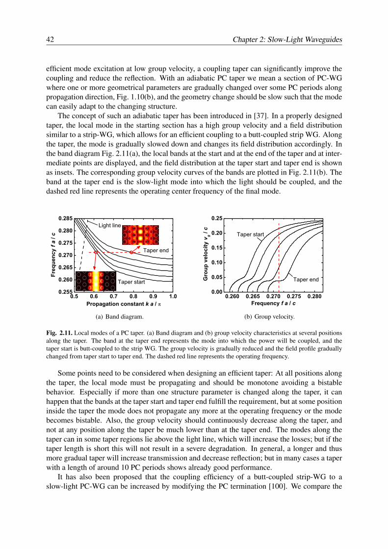
42 Chapter 2: Slow-Light Waveguides
efficient mode excitation at low group velocity, a coupling taper can significantly improve thecoupling and reduce the reflection. With an adiabatic PC taper we mean a section of PC-WGwhere one or more geometrical parameters are gradually changed over some PC periods alongpropagation direction, Fig. 1.10(b), and the geometry change should be slow such that the modecan easily adapt to the changing structure.
The concept of such an adiabatic taper has been introduced in [37]. In a properly designedtaper, the local mode in the starting section has a high group velocity and a field distributionsimilar to a strip-WG, which allows for an efficient coupling to a butt-coupled strip WG. Alongthe taper, the mode is gradually slowed down and changes its field distribution accordingly. Inthe band diagram Fig. 2.11(a), the local bands at the start and at the end of the taper and at inter-mediate points are displayed, and the field distribution at the taper start and taper end is shownas insets. The corresponding group velocity curves of the bands are plotted in Fig. 2.11(b). Theband at the taper end is the slow-light mode into which the light should be coupled, and thedashed red line represents the operating center frequency of the final mode.
0.5 0.6 0.7 0.8 0.9 1.00.255
0.260
0.265
0.270
0.275
0.280
0.285
Taper end
Taper start
Light line
Freq
uenc
y f a
/ c
Propagation constant k a /
(a) Band diagram.
0.260 0.265 0.270 0.275 0.2800.00
0.05
0.10
0.15
0.20
0.25
Taper endGro
up v
eloc
ity v
g / c
Frequency f a / c
Taper start
(b) Group velocity.
Fig. 2.11. Local modes of a PC taper. (a) Band diagram and (b) group velocity characteristics at several positionsalong the taper. The band at the taper end represents the mode into which the power will be coupled, and thetaper start is butt-coupled to the strip WG. The group velocity is gradually reduced and the field profile graduallychanged from taper start to taper end. The dashed red line represents the operating frequency.
Some points need to be considered when designing an efficient taper: At all positions alongthe taper, the local mode must be propagating and should be monotone avoiding a bistablebehavior. Especially if more than one structure parameter is changed along the taper, it canhappen that the bands at the taper start and taper end fulfill the requirement, but at some positioninside the taper the mode does not propagate any more at the operating frequency or the modebecomes bistable. Also, the group velocity should continuously decrease along the taper, andnot at any position along the taper be much lower than at the taper end. The modes along thetaper can in some taper regions lie above the light line, which will increase the losses; but if thetaper length is short this will not result in a severe degradation. In general, a longer and thusmore gradual taper will increase transmission and decrease reflection; but in many cases a taperwith a length of around 10 PC periods shows already good performance.
It has also been proposed that the coupling efficiency of a butt-coupled strip-WG to aslow-light PC-WG can be increased by modifying the PC termination [100]. We compare the
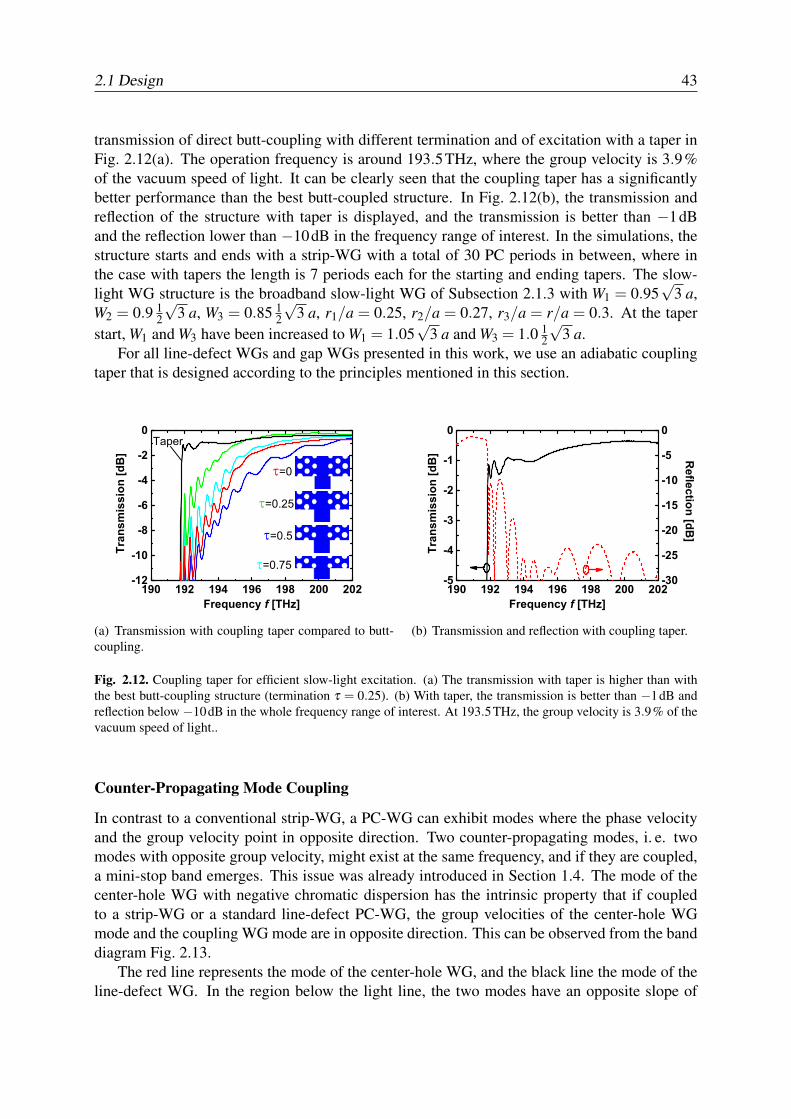
2.1 Design 43
transmission of direct butt-coupling with different termination and of excitation with a taper inFig. 2.12(a). The operation frequency is around 193.5THz, where the group velocity is 3.9%of the vacuum speed of light. It can be clearly seen that the coupling taper has a significantlybetter performance than the best butt-coupled structure. In Fig. 2.12(b), the transmission andreflection of the structure with taper is displayed, and the transmission is better than −1dBand the reflection lower than −10dB in the frequency range of interest. In the simulations, thestructure starts and ends with a strip-WG with a total of 30 PC periods in between, where inthe case with tapers the length is 7 periods each for the starting and ending tapers. The slow-light WG structure is the broadband slow-light WG of Subsection 2.1.3 with W1 = 0.95
√3 a,
W2 = 0.9 12
√3 a, W3 = 0.85 1
2
√3 a, r1/a = 0.25, r2/a = 0.27, r3/a = r/a = 0.3. At the taper
start, W1 and W3 have been increased to W1 = 1.05√
3 a and W3 = 1.0 12
√3 a.
For all line-defect WGs and gap WGs presented in this work, we use an adiabatic couplingtaper that is designed according to the principles mentioned in this section.
190 192 194 196 198 200 202-12
-10
-8
-6
-4
-2
0
=0.25
=0.75
=0.5
=0
Tran
smis
sion
[dB
]
Frequency f [THz]
Taper
(a) Transmission with coupling taper compared to butt-coupling.
190 192 194 196 198 200 202-5
-4
-3
-2
-1
0
-30
-25
-20
-15
-10
-5
0Tr
ansm
issi
on [d
B]
Frequency f [THz]
Reflection [dB
]
(b) Transmission and reflection with coupling taper.
Fig. 2.12. Coupling taper for efficient slow-light excitation. (a) The transmission with taper is higher than withthe best butt-coupling structure (termination τ = 0.25). (b) With taper, the transmission is better than −1dB andreflection below −10dB in the whole frequency range of interest. At 193.5THz, the group velocity is 3.9% of thevacuum speed of light..
Counter-Propagating Mode Coupling
In contrast to a conventional strip-WG, a PC-WG can exhibit modes where the phase velocityand the group velocity point in opposite direction. Two counter-propagating modes, i. e. twomodes with opposite group velocity, might exist at the same frequency, and if they are coupled,a mini-stop band emerges. This issue was already introduced in Section 1.4. The mode of thecenter-hole WG with negative chromatic dispersion has the intrinsic property that if coupledto a strip-WG or a standard line-defect PC-WG, the group velocities of the center-hole WGmode and the coupling WG mode are in opposite direction. This can be observed from the banddiagram Fig. 2.13.
The red line represents the mode of the center-hole WG, and the black line the mode of theline-defect WG. In the region below the light line, the two modes have an opposite slope of
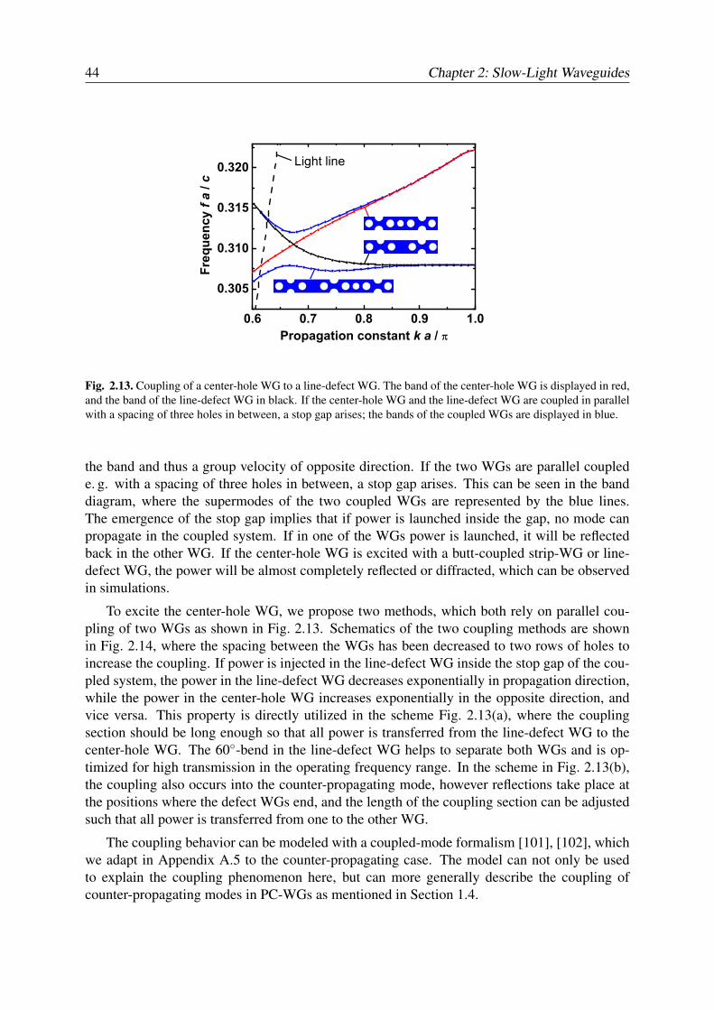
44 Chapter 2: Slow-Light Waveguides
0.6 0.7 0.8 0.9 1.0
0.305
0.310
0.315
0.320 Light line
Freq
uenc
y f a
/ c
Propagation constant k a /
Fig. 2.13. Coupling of a center-hole WG to a line-defect WG. The band of the center-hole WG is displayed in red,and the band of the line-defect WG in black. If the center-hole WG and the line-defect WG are coupled in parallelwith a spacing of three holes in between, a stop gap arises; the bands of the coupled WGs are displayed in blue.
the band and thus a group velocity of opposite direction. If the two WGs are parallel couplede. g. with a spacing of three holes in between, a stop gap arises. This can be seen in the banddiagram, where the supermodes of the two coupled WGs are represented by the blue lines.The emergence of the stop gap implies that if power is launched inside the gap, no mode canpropagate in the coupled system. If in one of the WGs power is launched, it will be reflectedback in the other WG. If the center-hole WG is excited with a butt-coupled strip-WG or line-defect WG, the power will be almost completely reflected or diffracted, which can be observedin simulations.
To excite the center-hole WG, we propose two methods, which both rely on parallel cou-pling of two WGs as shown in Fig. 2.13. Schematics of the two coupling methods are shownin Fig. 2.14, where the spacing between the WGs has been decreased to two rows of holes toincrease the coupling. If power is injected in the line-defect WG inside the stop gap of the cou-pled system, the power in the line-defect WG decreases exponentially in propagation direction,while the power in the center-hole WG increases exponentially in the opposite direction, andvice versa. This property is directly utilized in the scheme Fig. 2.13(a), where the couplingsection should be long enough so that all power is transferred from the line-defect WG to thecenter-hole WG. The 60-bend in the line-defect WG helps to separate both WGs and is op-timized for high transmission in the operating frequency range. In the scheme in Fig. 2.13(b),the coupling also occurs into the counter-propagating mode, however reflections take place atthe positions where the defect WGs end, and the length of the coupling section can be adjustedsuch that all power is transferred from one to the other WG.
The coupling behavior can be modeled with a coupled-mode formalism [101], [102], whichwe adapt in Appendix A.5 to the counter-propagating case. The model can not only be usedto explain the coupling phenomenon here, but can more generally describe the coupling ofcounter-propagating modes in PC-WGs as mentioned in Section 1.4.
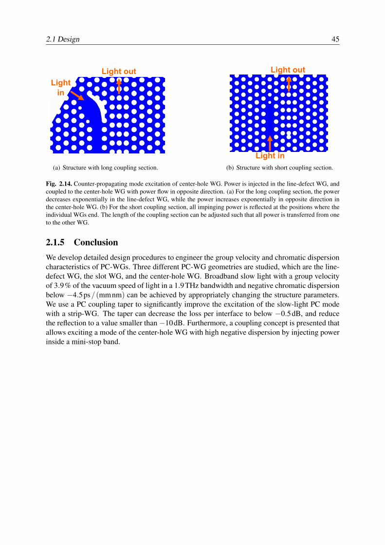
2.1 Design 45
(a) Structure with long coupling section. (b) Structure with short coupling section.
Fig. 2.14. Counter-propagating mode excitation of center-hole WG. Power is injected in the line-defect WG, andcoupled to the center-hole WG with power flow in opposite direction. (a) For the long coupling section, the powerdecreases exponentially in the line-defect WG, while the power increases exponentially in opposite direction inthe center-hole WG. (b) For the short coupling section, all impinging power is reflected at the positions where theindividual WGs end. The length of the coupling section can be adjusted such that all power is transferred from oneto the other WG.
2.1.5 ConclusionWe develop detailed design procedures to engineer the group velocity and chromatic dispersioncharacteristics of PC-WGs. Three different PC-WG geometries are studied, which are the line-defect WG, the slot WG, and the center-hole WG. Broadband slow light with a group velocityof 3.9% of the vacuum speed of light in a 1.9THz bandwidth and negative chromatic dispersionbelow −4.5ps/(mmnm) can be achieved by appropriately changing the structure parameters.We use a PC coupling taper to significantly improve the excitation of the slow-light PC modewith a strip-WG. The taper can decrease the loss per interface to below −0.5dB, and reducethe reflection to a value smaller than −10dB. Furthermore, a coupling concept is presented thatallows exciting a mode of the center-hole WG with high negative dispersion by injecting powerinside a mini-stop band.

46 Chapter 2: Slow-Light Waveguides
2.2 Imperfections 47
2.2 Imperfections
Light propagation inside a PC-WG is theoretically lossless if the mode stays below the light lineand if material losses are negligible. However, extrinsic losses caused by imperfect fabricationprocesses limit the performance of PC devices significantly. Disorder-induced losses in PC-WGs have considerably decreased over the last years, as much effort has been made to improvethe SOI fabrication processes and to understand the loss mechanisms in PCs. The lowest lossesreported in a silicon membrane W1-WG are 4.1dB/cm [42], which is a value that can betolerated for small integrated optical devices. The lowest losses in a PC-WG, however, occurat high group velocities, while disorder-induced losses considerably increase with decreasinggroup velocity. Based on a theoretical model supported by experimental data [59], the lossesobey a quadratic law α ∝ 1/v2
g in the case of dominant backscattering losses occurring at lowgroup velocities, and have a linear relation α ∝ 1/vg in the case of dominant out-of-plane lossesat higher group velocities. Another experimental work [103] suggests a square root law α ∝1/√vg for dominant out-of-plane losses at group velocities above 5% of the vacuum speed of
light. These different findings show that so far, the dependence of losses on group velocity isnot well understood. Furthermore, methods to minimize losses for slow-light WGs have notbeen presented in detail.
The dependance of scattering losses on the disorder root mean square value σ is quadratic,α ∝ σ2, which has been theoretically and experimentally well proven [57], [103].
In this section, we numerically investigate the effects of radial disorder on broadband slow-light PC-WGs. We seek to develop broadband slow-light WGs with minimum losses, whichalso requires to gain more insights into the effect of low group velocity on the disorder-inducedlosses. To this end, we design various broadband slow-light structures that all exhibit a groupvelocity of about 4% of the vacuum speed of light in a bandwidth of more than 1THz. Thedisorder-induced losses of the designs are numerically determined and compared. Two nu-merical methods are used, which are the FIT and the GME methods, and the suitability andlimitations of both methods are discussed. In order to minimize losses, we find that the PC-WG should be single-moded, otherwise disorder-induced mode coupling occurs that leads toincreased losses. Furthermore, increasing the core width of a WG can decrease losses, as longas the WG is still single-moded. For a structure that is not vertically symmetric, like a SOIstructure, intrinsic mode coupling between the previously orthogonal TE and TM modes oc-cur, which can lead to mode gaps which considerably increase losses. A single-moded PC-WGwith a vertically symmetric structure, like a membrane structure or a SOI structure with glasscladding, has thus lowest losses. The group velocity behavior of the broadband slow-light WGis only slightly changed by the presence of disorder, which is an important property. Further-more, we examine the relation between disorder-induced losses and group velocity, but contrastto the above mentioned published results we find that simple relations like a quadratic, linear orsquare root law do not adequately reflect the behavior.
This section is structured as follows: In Subsection 2.2.1, the parameters to characterizelosses are specified and a model is introduced to determine transmission and reflection of aWG from these loss parameters. Subsection 2.2.2 discusses the two numerical methods FITand GME to determine losses. In Subsection 2.2.3, the different broadband slow-light designsare presented, and in Subsection 2.2.4 the loss results are presented and discussed. Finally, thedependance of the losses on the group velocity characteristic is treated in Subsection 2.2.5.
48 Chapter 2: Slow-Light Waveguides
2.2.1 Loss Parameters and Loss Model
The losses of a PC-WG can be quantified by loss parameters α , as already introduced in Sec-tion 1.6. The out-of-plane loss αo results from the coupling of the WG mode to radiation modesthat can propagate in the half-spaces below or above the silicon slab, which can be caused bymode operation above the light line or by the existence of structural disorder. The backscatter-ing loss αb is caused by the disorder-induced coupling of a forward propagating mode with therespective backwards propagating mode. The in-plane loss αp quantifies the leakage of powerout of the WG into the silicon slab plane, which can be caused by an insufficient number of rowof holes next to the WG core, or by a missing or insufficient bulk bandgap in the presence of dis-order. In our case, we expect the in-plane loss to be very small, and we model residual in-planeloss as part of the out-of-plane loss. If the PC-WG is multi-moded, disorder can also lead tocoupling of the desired mode with other forward or backwards propagating modes. Similarly, avertical structure asymmetry can couple the originally separable TE and TM modes, where thevertical asymmetry can be either intrinsic, as for an SOI structure, or again caused by disorder.The mode coupling to other guided modes also effectively increases losses, as the other modesexhibit undesirable group velocity characteristics, and as converted power is not coupled out tothe connecting WGs. We will also model mode coupling effects as part of the out-of-plane loss.Thus, we characterize the losses by the two parameters αo and αb, and the total loss αt is thesum of the two parameters, αt = αo +αb.
For a PC-WG of length L, the presence of losses decreases the transmitted power and in-creases the reflected power in comparison to the lossless structure. In all measurements andfully-numerical methods like FIT, the transmission and reflection characteristics are determinedrather than the loss parameters. Thus, we need to introduce a loss model to be able to link thetransmission and reflection with the loss parameters. The loss model is based on the coupledpower equations of Marcuse [104], [105], and schematically shown in Fig. 2.15. The powertraveling to the right Pr is diminished by the out-of-plane scattering αo and by the backscatter-ing αb, while it is increased by the backscattering αb from the mode traveling to the left. Theanalog behavior applies for the power traveling to the left, Pl. In the coupled power equations,the powers Pr and Pl stand for ensemble averaged values. In the derivation of the coupled powerequations, perturbation theory is used, which is strictly valid only for weak coupling. However,even in the case of strong coupling, the equations can be used if the loss coefficients are fittedto measurement or simulation results. The differential equations that govern the power flow tothe left Pl(z) and to the right Pr(z) as function of position can be formulated as:
dPr(z)dz
=−(αb +αo)Pr +αbPl , (2.1)
dPl(z)dz
= (αb +αo)Pl−αbPr . (2.2)

2.2 Imperfections 49
Pr
Pl
Pr L
zL
o
b
o
b
Pr z
Pl z
Fig. 2.15. Loss model for a PC-WG with out-of-plane and backscattering loss. The out-of-plane and backscatteringloss parameters are ao and αb, respectively. The power traveling to the left and right is denoted as Pl and Pr,respectively, and the transmitted and backscattered power of a WG of length L is Pr(L) and Pl(0), respectively, foran injected power Pr(0).
The differential equations Eq. (2.1) and Eq. (2.2) are solved using the boundary conditionsPl(L) = 0 (reflected power at z = L is zero) and Pr(0) = 1 (injected power at z = 0 is unity), andthe normalized transmission Pr(L) and normalized reflection Pl(0) are found (Appendix A.6):
Pl(0) =αb tanh(αL)
αt tanh(αL)+α, (2.3)
Pr(L) =αb
αsinh(αL)Pl(0)+ cosh(αL)− αt
αsinh(αL) , (2.4)
αt = αb +αo , α =√
α2t −α2
b =√
α2o +2αbαo . (2.5)
The normalized powers Pl(0) and Pr(L) are in the range between 0 and 1, and the total powertransmitted in positive z-direction is Ptot(z) = Pr(z)−Pl(z).
The results in Eqs. (2.3)-(2.5) are hard to understand intuitively, and in order to gain morephysical insight into the behavior the model Eqs. (2.1)-(2.2) is simplified:
dPr(z)dz
=−(αb +αo)Pr , (2.6)
dPl(z)dz
=−αbPr . (2.7)
On the right hand sides of the equations, the terms involving the power traveling to the leftare neglected, as the power traveling to the left should be much smaller than the power trav-eling to the right. The solution using the same boundary conditions as above is found to be(Appendix A.6):
Pl(0) =αb
αt
(1− e−αtL
), (2.8)
Pr(L) = e−αtL . (2.9)
The transmission, Eq. (2.9), obeys the commonly used exponential relation. For a small productof total loss and length, αtL ¿ 1, the backreflection Eq. (2.8) can be approximated by Pl(0) =αbL. For large WG lengths, the backreflection Pl(0) approaches the upper limit αb/αt.
50 Chapter 2: Slow-Light Waveguides
The lossy WG can also be represented as a linear two-port network where the first port islocated at position z = 0 and the second port at z = L. The network can be described by its fourscattering parameters Sij, i, j = 1,2, which relate the outgoing complex wave amplitudes bj atport j with the incoming wave amplitudes ai at port i by bj = ∑i Sjiai. The square of the absolutevalues of the scattering parameters correspond to the normalized powers of Eqs. (2.3)-(2.5) orEqs. (2.8)-(2.9), |S11|2 = Pl(0) and |S21|2 = Pr(L).
2.2.2 Numerical MethodsFor the numerical determination of disorder-induced losses, two methods are used, which arethe GME and FIT methods, see also Appendix A.2. Here we discuss the suitability and relia-bility of the two methods for the simulation of losses.
The FIT is a fully-numerical method that solves Maxwell’s equations at discrete times andin a discretized 3D space. In general, all possible structures can be simulated, and all lineareffects that lead to losses are taken into account. Numerical errors are mainly caused by thelimited structure discretization and a finite simulation time. We show in Subsection 4.3.2 thatresults from disorder simulations for both a single realization of a disordered structure and forensemble averages agree very well with results from FDTD, which gives a high credibility tothe FIT results. The main drawback of the method is, however, that the simulation time is verylong, which limits the number of structures that can be simulated in an acceptable time.
On the other hand, the GME method is very fast, as it is a semianalytical method thatuses a perturbative approach to determine losses. However, it is not an exact method and onlyconsiders coupling to radiative modes and to the counter-propagating mode, whereas modecoupling with other guided modes is not taken into account. Thus, the losses of multi-modedor vertically asymmetric WGs can not be reliably simulated with the GME method. Also forsingle-moded and vertically symmetric WGs, we expect the loss results from GME to be lessaccurate than those from FIT, as outlined in Subsection 4.3.2. But if properly used, the GMEmethod allows a quick comparison of a large number of structures.
2.2.3 Broadband Slow-Light StructuresThe disorder-induced losses of a PC-WG show a strong dependance on the group velocity ofthe mode, as already mentioned in the introduction of the section. Thus, to compare the lossesof different slow-light structures, the group velocity characteristics need to be similar. If thestructure of a PC-WG is optimized to exhibit low losses, e. g. using automatic algorithms, itwill ultimately lead to designs with high group velocity. Here, we choose to fix the groupvelocity behavior and find different designs based on a line-defect WG that lead to a similarcharacteristics.
We show six different broadband designs that exhibit a group velocity of 3.7% of thevacuum speed of light at an operating frequency of 193.4THz or an operating wavelengthof 1.55 µm. In addition, a standard W1-WG is chosen as reference. The broadband slow-light WGs are designed with the GME method according to the principles presented in Sec-tion 2.1. The lattice constant a for all designs is adjusted such that the operating frequency is at193.4THz. The structures with the corresponding parameters are summarized in Table 2.1, andstructure schematics are shown in Fig. 2.16.
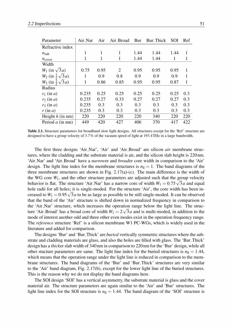
2.2 Imperfections 51
Parameter Air Nar Air Air Broad Bur Bur Thick SOI RefRefractive indexnsub 1 1 1 1.44 1.44 1.44 1ncover 1 1 1 1.44 1.44 1 1WidthW1 (in
√3a) 0.75 0.95 2 0.95 0.95 0.95 1
W2 (in 12
√3a) 1 0.9 0.8 0.9 0.9 0.9 1
W3 (in 12
√3a) 1 0.86 0.85 0.95 0.95 0.87 1
Radiusr1 (in a) 0.235 0.25 0.25 0.25 0.25 0.25 0.3r2 (in a) 0.235 0.27 0.33 0.27 0.27 0.27 0.3r3 (in a) 0.235 0.3 0.3 0.3 0.3 0.3 0.3r (in a) 0.235 0.3 0.3 0.3 0.3 0.3 0.3Height h (in nm) 220 220 220 220 340 220 220Period a (in nm) 449 420 427 406 370 417 422
Table 2.1. Structure parameters for broadband slow light designs. All structures except for the ‘Ref’ structure aredesigned to have a group velocity of 3.7% of the vacuum speed of light at 193.4THz in a large bandwidth.
The first three designs ‘Air Nar’, ‘Air’ and ‘Air Broad’ are silicon air membrane struc-tures, where the cladding and the substrate material is air, and the silicon slab height is 220nm.‘Air Nar’ and ‘Air Broad’ have a narrower and broader core width in comparison to the ‘Air’design. The light line index for the membrane structures is nll = 1. The band diagrams of thethree membrane structures are shown in Fig. 2.17(a)-(c). The main difference is the width ofthe WG core W1, and the other structure parameters are adjusted such that the group velocitybehavior is flat. The structure ‘Air Nar’ has a narrow core of width W1 = 0.75
√3a and equal
hole radii for all holes; it is single-moded. For the structure ‘Air’, the core width has been in-creased to W1 = 0.95
√3a to be as large as possible to be still single-moded. It can be observed
that the band of the ‘Air’ structure is shifted down in normalized frequency in comparison tothe ‘Air Nar’ structure, which increases the operation range below the light line. The struc-ture ‘Air Broad’ has a broad core of width W1 = 2
√3a and is multi-moded, in addition to the
mode of interest another odd and three other even modes exist in the operation frequency range.The reference structure ‘Ref’ is a silicon membrane W1 PC-WGs, which is widely used in theliterature and added for comparison.
The designs ‘Bur’ and ‘Bur Thick’ are buried vertically symmetric structures where the sub-strate and cladding materials are glass, and also the holes are filled with glass. The ‘Bur Thick’design has a thicker slab width of 340nm in comparison to 220nm for the ‘Bur’ design, while allother stucture parameters are same. The light line index for the buried structures is nll = 1.44,which means that the operation range under the light line is reduced in comparison to the mem-brane structures. The band diagrams of the ‘Bur’ and ‘Bur Thick’ structures are very similarto the ‘Air’ band diagram, Fig. 2.17(b), except for the lower light line of the buried structures.This is the reason why we do not display the band diagrams here.
The SOI design ‘SOI’ has a vertical asymmetry, the substrate material is glass and the covermaterial air. The structure parameters are again similar to the ‘Air’ and ‘Bur’ structures. Thelight line index for the SOI structure is nll = 1.44. The band diagram of the ‘SOI’ structure is
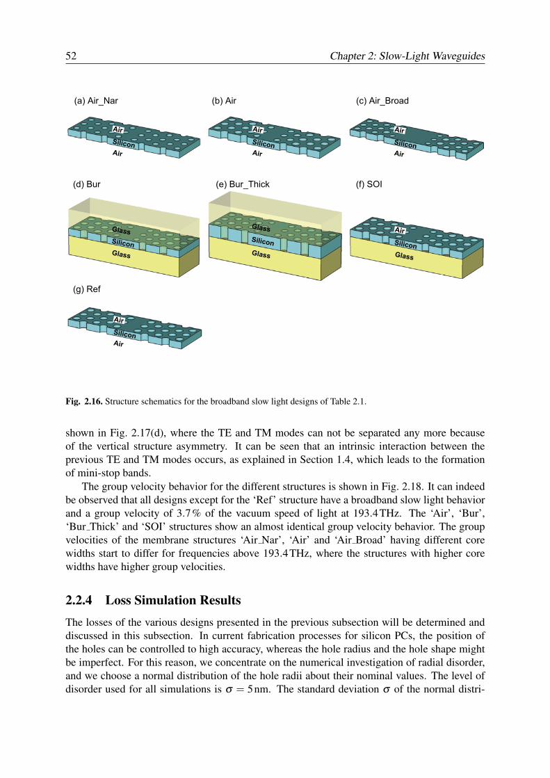
52 Chapter 2: Slow-Light Waveguides
Fig. 2.16. Structure schematics for the broadband slow light designs of Table 2.1.
shown in Fig. 2.17(d), where the TE and TM modes can not be separated any more becauseof the vertical structure asymmetry. It can be seen that an intrinsic interaction between theprevious TE and TM modes occurs, as explained in Section 1.4, which leads to the formationof mini-stop bands.
The group velocity behavior for the different structures is shown in Fig. 2.18. It can indeedbe observed that all designs except for the ‘Ref’ structure have a broadband slow light behaviorand a group velocity of 3.7% of the vacuum speed of light at 193.4THz. The ‘Air’, ‘Bur’,‘Bur Thick’ and ‘SOI’ structures show an almost identical group velocity behavior. The groupvelocities of the membrane structures ‘Air Nar’, ‘Air’ and ‘Air Broad’ having different corewidths start to differ for frequencies above 193.4THz, where the structures with higher corewidths have higher group velocities.
2.2.4 Loss Simulation ResultsThe losses of the various designs presented in the previous subsection will be determined anddiscussed in this subsection. In current fabrication processes for silicon PCs, the position ofthe holes can be controlled to high accuracy, whereas the hole radius and the hole shape mightbe imperfect. For this reason, we concentrate on the numerical investigation of radial disorder,and we choose a normal distribution of the hole radii about their nominal values. The level ofdisorder used for all simulations is σ = 5nm. The standard deviation σ of the normal distri-
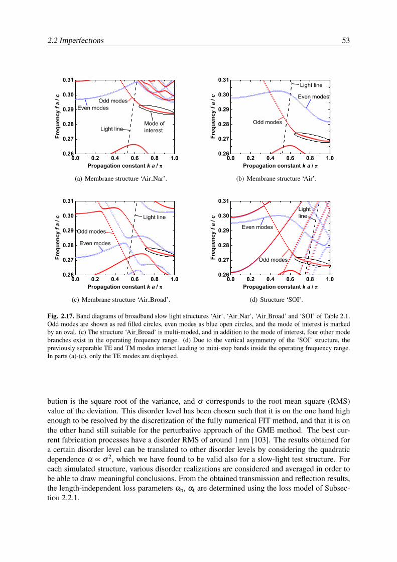
2.2 Imperfections 53
0.0 0.2 0.4 0.6 0.8 1.00.26
0.27
0.28
0.29
0.30
0.31
Mode of interestLight line
Freq
uenc
y f a
/ c
Propagation constant k a /
Odd modesEven modes
(a) Membrane structure ‘Air Nar’.
0.0 0.2 0.4 0.6 0.8 1.00.26
0.27
0.28
0.29
0.30
0.31Light line
Freq
uenc
y f a
/ c
Propagation constant k a /
Odd modes
Even modes
(b) Membrane structure ‘Air’.
0.0 0.2 0.4 0.6 0.8 1.00.26
0.27
0.28
0.29
0.30
0.31
Even modes
Light line
Freq
uenc
y f a
/ c
Propagation constant k a /
Odd modes
(c) Membrane structure ‘Air Broad’.
0.0 0.2 0.4 0.6 0.8 1.00.26
0.27
0.28
0.29
0.30
0.31
Odd modes
Lightline
Freq
uenc
y f a
/ c
Propagation constant k a /
Even modes
(d) Structure ‘SOI’.
Fig. 2.17. Band diagrams of broadband slow light structures ‘Air’, ‘Air Nar’, ‘Air Broad’ and ‘SOI’ of Table 2.1.Odd modes are shown as red filled circles, even modes as blue open circles, and the mode of interest is markedby an oval. (c) The structure ‘Air Broad’ is multi-moded, and in addition to the mode of interest, four other modebranches exist in the operating frequency range. (d) Due to the vertical asymmetry of the ‘SOI’ structure, thepreviously separable TE and TM modes interact leading to mini-stop bands inside the operating frequency range.In parts (a)-(c), only the TE modes are displayed.
bution is the square root of the variance, and σ corresponds to the root mean square (RMS)value of the deviation. This disorder level has been chosen such that it is on the one hand highenough to be resolved by the discretization of the fully numerical FIT method, and that it is onthe other hand still suitable for the perturbative approach of the GME method. The best cur-rent fabrication processes have a disorder RMS of around 1nm [103]. The results obtained fora certain disorder level can be translated to other disorder levels by considering the quadraticdependence α ∝ σ2, which we have found to be valid also for a slow-light test structure. Foreach simulated structure, various disorder realizations are considered and averaged in order tobe able to draw meaningful conclusions. From the obtained transmission and reflection results,the length-independent loss parameters αb, αt are determined using the loss model of Subsec-tion 2.2.1.
54 Chapter 2: Slow-Light Waveguides
192 194 196 198 2000.00
0.05
0.10
0.15
0.20
Air_Nar Air Air_Broad Bur Bur_Thick SOI Ref
Gro
up v
eloc
ity v
g / c
Frequency f [THz]
Fig. 2.18. Group velocity for broadband slow light designs of Table 2.1. All designs except the reference structureexhibit a broadband slow light behavior with a group velocity of 3.7% of the vacuum speed of light at 193.4THz.
FIT Method
We evaluate the losses of four slow-light designs using the FIT method. Because of the longsimulation times it is not possible to simulate all suggested designs of the previous subsection,therefore we restrict ourselves to the two single-moded WGs ‘Air’ and ‘Bur’, the multi-modedWG ‘Air Broad’ and the vertically asymmetric structure ‘SOI’. Significant mode-coupling ef-fects are expected for the ‘Air Broad’ and ‘SOI’ structures, which can be considered using theFIT method. The length of the disordered section is 15 periods, and to efficiently couple tothe slow light mode with a strip-WG, a PC taper with a length of 5 periods and 2 additionaltransition periods on each side of the taper was introduced at the beginning and at the end of thedisordered section. To remove the influence of these coupling sections from the transmissionand reflection results, a numerical calibration technique is used. This is the transmission-reflect-line (TRL) calibration; more details on this technique are presented in Subsection 4.3.2, and themathematical background can be found in Appendix A.4. A number of 25 different disor-der realizations were simulated for each of the structures, and the transmission and reflectionresults were averaged over the realizations. The calibrated and averaged transmission character-istics are shown in Fig. 2.19. The solid lines represent the averaged transmission with disorder,whereas the dashed lines show the transmission for the ideal structures. It is to be noted thatthe length 15a of the PC-WG is different for the different structures, as the period a is not thesame for all designs, Table 2.1. For the ideal structures, the transmission below the light lineshould be near 0dB, which can indeed be observed for the ‘Air’, ‘Air Broad’ and ‘Bur’ struc-tures. In certain spectral ranges, however, the transmission rises to values above 0dB, whichis caused by numerical errors; this can be especially seen for the ‘Air Broad’ and ‘Bur’ struc-tures around 194THz. The light-line intersection point for the ‘Bur’ structure can be localizednear 194.3THz. For lower frequencies, the mode is below the light line, while for higher fre-quencies the mode becomes leaky and the ideal transmission drops. For the ‘SOI’ structure,however, the ideal transmission below the light line is much lower than for all other structures,

2.2 Imperfections 55
192 194 196 198 200 202 204-2.5
-2.0
-1.5
-1.0
-0.5
0.0Air: With disorder
SOI: With disorder
Air: No disorder
Tran
smis
sion
[dB
]
Frequency f [THz]
SOI: No disorder
(a) Transmission for ‘Air’ and ‘SOI’.
192 194 196 198 200 202 204-2.5
-2.0
-1.5
-1.0
-0.5
0.0
Air_Broad: With disorder
Bur: With disorder
Air_Broad: No disorder
Bur: No disorder
Tran
smis
sion
[dB
]
Frequency f [THz]
(b) Transmission for ‘Air Broad’ and ‘Bur’.
Fig. 2.19. Transmission with and without disorder from FIT-simulations for structures ‘Air’, ‘Bur’, ‘Air Broad’ and‘SOI’ of Table 2.1. (a) For ‘Air’, the ideal transmission is near 0dB. For ‘SOI’, the transmission without disorderis already low, which indicates intrinsic TE-TM mode coupling. (b) For ‘Bur’, the transmission drop caused by thelight-line intersection near 194.3THz is observed. The ideal transmission for both ‘Bur’ and ‘Air Broad’ is largerthan 0dB indicating numerical errors.
and the disorder reduces the transmission only marginally; also the light-line intersection can-not be observed. This indicates that the ‘SOI’ structure exhibits very large intrinsic losses, andwe propose that these are caused by TE-TM coupling which exists even without disorder.
The group velocity curves for the structures with disorder are shown in Fig. 2.20. The in-fluence of the disorder on the group velocity in the broadband slow-light region is only slightwhich implies that the broadband slow light characteristics are not significantly impeded. Onlyabove 196THz, oscillations arise at certain frequencies in the spectrum, which can be attributedto mode coupling. It is to be noted that the group velocity characteristics from the FIT methoddeviates somewhat from the group velocity obtained from GME, Fig. 2.18, which is most likely
192 194 196 198 200 202 2040.00
0.05
0.10
0.15
0.20
0.25SOI
Bur
Air_Broad
Gro
up v
eloc
ity v
g / c
Frequency f [THz]
Air
Fig. 2.20. Group velocity for disordered structures ‘Air’, ‘Bur’, ‘Air Broad’ and ‘SOI’ of Table 2.1 from FITsimulations. The disorder affects the group velocity only slightly, and the broadband slow light behavior persists.Only above 196THz, oscillations due to mode coupling occur. For the ‘Air Broad’ structure, the group velocitydeviates from what is expected.
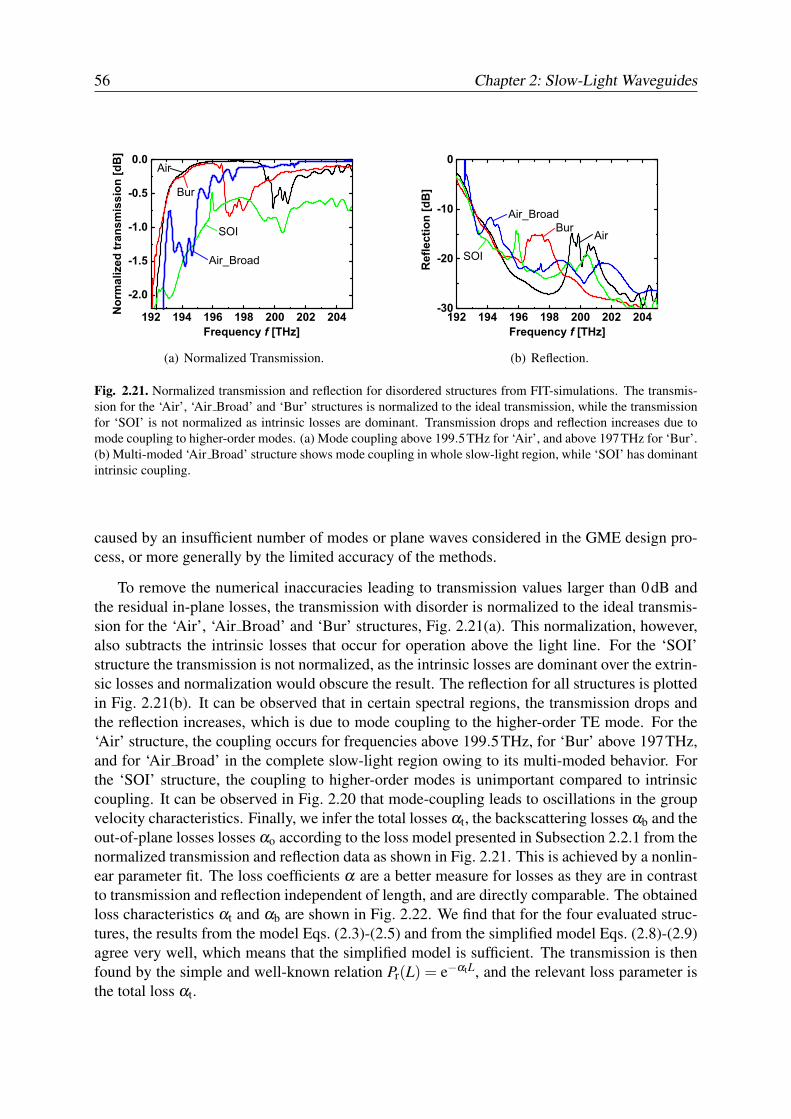
56 Chapter 2: Slow-Light Waveguides
192 194 196 198 200 202 204
-2.0
-1.5
-1.0
-0.5
0.0
Nor
mal
ized
tran
smis
sion
[dB
]
Frequency f [THz]
Bur
Air
Air_Broad
SOI
(a) Normalized Transmission.
192 194 196 198 200 202 204-30
-20
-10
0
Ref
lect
ion
[dB
]
Frequency f [THz]
SOI
Air_BroadBur
Air
(b) Reflection.
Fig. 2.21. Normalized transmission and reflection for disordered structures from FIT-simulations. The transmis-sion for the ‘Air’, ‘Air Broad’ and ‘Bur’ structures is normalized to the ideal transmission, while the transmissionfor ‘SOI’ is not normalized as intrinsic losses are dominant. Transmission drops and reflection increases due tomode coupling to higher-order modes. (a) Mode coupling above 199.5THz for ‘Air’, and above 197THz for ‘Bur’.(b) Multi-moded ‘Air Broad’ structure shows mode coupling in whole slow-light region, while ‘SOI’ has dominantintrinsic coupling.
caused by an insufficient number of modes or plane waves considered in the GME design pro-cess, or more generally by the limited accuracy of the methods.
To remove the numerical inaccuracies leading to transmission values larger than 0dB andthe residual in-plane losses, the transmission with disorder is normalized to the ideal transmis-sion for the ‘Air’, ‘Air Broad’ and ‘Bur’ structures, Fig. 2.21(a). This normalization, however,also subtracts the intrinsic losses that occur for operation above the light line. For the ‘SOI’structure the transmission is not normalized, as the intrinsic losses are dominant over the extrin-sic losses and normalization would obscure the result. The reflection for all structures is plottedin Fig. 2.21(b). It can be observed that in certain spectral regions, the transmission drops andthe reflection increases, which is due to mode coupling to the higher-order TE mode. For the‘Air’ structure, the coupling occurs for frequencies above 199.5THz, for ‘Bur’ above 197THz,and for ‘Air Broad’ in the complete slow-light region owing to its multi-moded behavior. Forthe ‘SOI’ structure, the coupling to higher-order modes is unimportant compared to intrinsiccoupling. It can be observed in Fig. 2.20 that mode-coupling leads to oscillations in the groupvelocity characteristics. Finally, we infer the total losses αt, the backscattering losses αb and theout-of-plane losses losses αo according to the loss model presented in Subsection 2.2.1 from thenormalized transmission and reflection data as shown in Fig. 2.21. This is achieved by a nonlin-ear parameter fit. The loss coefficients α are a better measure for losses as they are in contrastto transmission and reflection independent of length, and are directly comparable. The obtainedloss characteristics αt and αb are shown in Fig. 2.22. We find that for the four evaluated struc-tures, the results from the model Eqs. (2.3)-(2.5) and from the simplified model Eqs. (2.8)-(2.9)agree very well, which means that the simplified model is sufficient. The transmission is thenfound by the simple and well-known relation Pr(L) = e−αtL, and the relevant loss parameter isthe total loss αt.
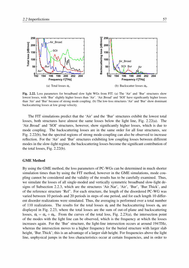
2.2 Imperfections 57
192 194 196 198 200 202 2040
50
100
150
200
250
SOI
Bur
Air_Broad
Tota
l los
s [d
B/m
m]
Frequency f [THz]
Air
(a) Total losses αt.
192 194 196 198 200 202 2040
50
100
150
200
250
Bac
ksca
tterin
g lo
ss [d
B/m
m]
Frequency f [THz]
AirBurSOI
Air_Broad
(b) Backscatter losses αb.
Fig. 2.22. Loss parameters for broadband slow light WGs from FIT. (a) The ‘Air’ and ‘Bur’ structures showlowest losses, with ‘Bur’ slightly higher losses than ‘Air’. ‘Air Broad’ and ‘SOI’ have significantly higher lossesthan ‘Air’ and ‘Bur’ because of strong mode coupling. (b) The low-loss structures ‘Air’ and ‘Bur’ show dominantbackscattering losses at low group velocity.
The FIT simulations predict that the ‘Air’ and the ‘Bur’ structures exhibit the lowest totallosses, both structures have almost the same losses below the light line, Fig. 2.22(a). The‘Air Broad’ and ‘SOI’ structures, however, show significantly higher losses, which is due tomode coupling. The backscattering losses are in the same order for all four structures, seeFig. 2.22(b), but the spectral regions of strong mode-coupling can also be observed to increasereflection. For the ‘Air’ and ‘Bur’ structures exhibiting low coupling losses between differentmodes in the slow-light regime, the backscattering losses become the significant contribution ofthe total losses, Fig. 2.22(b).
GME Method
By using the GME method, the loss parameters of PC-WGs can be determined in much shortersimulation times than by using the FIT method, however in the GME simulations, mode cou-pling cannot be considered and the validity of the results has to be carefully examined. Thus,we simulate the losses of all single-moded and vertically symmetric broadband slow-light de-signs of Subsection 2.2.3, which are the structures ‘Air Nar’, ‘Air’, ‘Bur’, ‘Bur Thick’, andof the reference structure ‘Ref’. For each structure, the length of the disordered PC-WG wasvaried between 10 periods and 20 periods in steps of one period, and for each length 10 differ-ent disorder realizations were simulated. Thus, the averaging is performed over a total numberof 110 realizations. The results for the total losses αt and the backscattering losses αb aredisplayed in Fig. 2.23, where the total losses are the sum of out-of-plane and backscatteringlosses, αt = αo + αb. From the curves of the total loss, Fig. 2.23(a), the intersection pointof the modes with the light line can be observed, which is the frequency at which the lossesincreases again. For the ‘Bur’ structure, the light-line intersection occurs at around 194THz,whereas the intersection moves to a higher frequency for the buried structure with larger slabheight, ‘Bur Thick’; this is an advantage of a larger slab height. For frequencies above the lightline, unphysical jumps in the loss characteristics occur at certain frequencies, and in order to
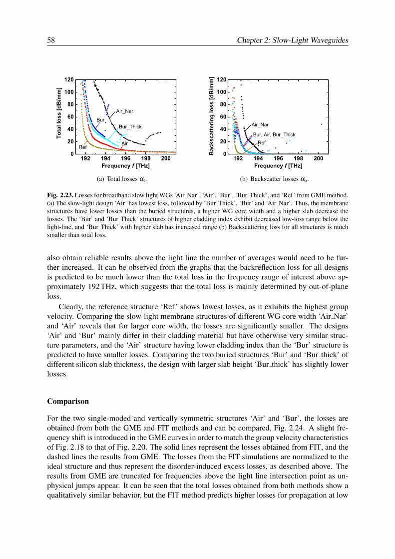
58 Chapter 2: Slow-Light Waveguides
192 194 196 198 2000
20
40
60
80
100
120
RefAir
Bur_ThickBur
Air_Nar
Tota
l los
s [d
B/m
m]
Frequency f [THz]
(a) Total losses αt.
192 194 196 198 2000
20
40
60
80
100
120
Bac
ksca
tterin
g lo
ss [d
B/m
m]
Frequency f [THz]
Air_Nar
Bur, Air, Bur_ThickRef
(b) Backscatter losses αb.
Fig. 2.23. Losses for broadband slow light WGs ‘Air Nar’, ‘Air’, ‘Bur’, ‘Bur Thick’, and ‘Ref’ from GME method.(a) The slow-light design ‘Air’ has lowest loss, followed by ‘Bur Thick’, ‘Bur’ and ‘Air Nar’. Thus, the membranestructures have lower losses than the buried structures, a higher WG core width and a higher slab decrease thelosses. The ‘Bur’ and ‘Bur Thick’ structures of higher cladding index exhibit decreased low-loss range below thelight-line, and ‘Bur Thick’ with higher slab has increased range (b) Backscattering loss for all structures is muchsmaller than total loss.
also obtain reliable results above the light line the number of averages would need to be fur-ther increased. It can be observed from the graphs that the backreflection loss for all designsis predicted to be much lower than the total loss in the frequency range of interest above ap-proximately 192THz, which suggests that the total loss is mainly determined by out-of-planeloss.
Clearly, the reference structure ‘Ref’ shows lowest losses, as it exhibits the highest groupvelocity. Comparing the slow-light membrane structures of different WG core width ‘Air Nar’and ‘Air’ reveals that for larger core width, the losses are significantly smaller. The designs‘Air’ and ‘Bur’ mainly differ in their cladding material but have otherwise very similar struc-ture parameters, and the ‘Air’ structure having lower cladding index than the ‘Bur’ structure ispredicted to have smaller losses. Comparing the two buried structures ‘Bur’ and ‘Bur thick’ ofdifferent silicon slab thickness, the design with larger slab height ‘Bur thick’ has slightly lowerlosses.
Comparison
For the two single-moded and vertically symmetric structures ‘Air’ and ‘Bur’, the losses areobtained from both the GME and FIT methods and can be compared, Fig. 2.24. A slight fre-quency shift is introduced in the GME curves in order to match the group velocity characteristicsof Fig. 2.18 to that of Fig. 2.20. The solid lines represent the losses obtained from FIT, and thedashed lines the results from GME. The losses from the FIT simulations are normalized to theideal structure and thus represent the disorder-induced excess losses, as described above. Theresults from GME are truncated for frequencies above the light line intersection point as un-physical jumps appear. It can be seen that the total losses obtained from both methods show aqualitatively similar behavior, but the FIT method predicts higher losses for propagation at low

2.2 Imperfections 59
192 194 196 198 200 202 2040
50
100
150
GME: BurGME: Air
FIT: Air
Tota
l los
s [d
B/m
m]
Frequency f [THz]
FIT: Bur
(a) Total loss αt.
192 194 196 198 200 202 2040
50
100
150
Bac
ksca
tter l
oss
[dB
/mm
]
Frequency f [THz]
GME: AirGME: Bur
FIT: BurFIT: Air
(b) Backscattering loss αb.
Fig. 2.24. Comparison of losses obtained from GME and FIT for ‘Air’ and ‘Bur’ structures. The FIT methodpredicts higher total loss at low group velocity and much higher backscattering loss than the GME method. Withboth methods, ‘Air’ has lower losses than ‘Bur’.
group velocity. At the same time, the reflection losses from the GME method are predicted tobe much lower than from the FIT method.
As discussed above, we assume the FIT method is more reliable than the GME method inpredicting losses, as the FIT method can model all loss effects and does not use any approxi-mations except for a limited structure discretization and simulation time. Furthermore, the lossresults from FIT are verified by results from FDTD for test structures, see Section 4.3. Al-though the results from the GME method do not agree perfectly, we suggest that the method iswell suited to compare the losses of PC-WGs that are single-moded and exhibit no significantmode-coupling, and because of its low simulation times it is ideal for structure optimization.
2.2.5 Dependance of Losses on Group Velocity
The disorder-induced losses of a PC mode are strongly dependent on its group velocity. Thelosses increase for decreasing group velocity, which can be observed in Fig. 2.22, where thegroup velocity decreases for decreasing frequencies. The increased losses at low group velocitycan be intuitively understood, as for a slower optical wave its interaction time with the scatterersis longer, or the possibility of a slow photon bouncing many times ‘back and forth’ is higher tobe scattered.
In three different works, the dependence of extrinsic losses with group velocity has beenpreviously studied; some of the findings have already been mentioned in the introduction of thissection. In [22], it has been identified that the propagation loss α is approximately inverselyproportional to group velocity vg, α ∝ 1
λ vg. In a physical model using Green’s functions [58]
it has been predicted and inferred from measurements [59] that the out-of-plane scattering lossscales inversely proportional with group velocity, αo ∝ 1
vg, and the backscattering loss scales
inversely proportional with the square of the group velocity, αb ∝ 1v2
g; for low group velocity,
the backscattering loss dominates. In [103] it was suggested that out-of-plane scattering isdominant for group velocities higher than 5% of the vacuum speed of light c and scales sub-
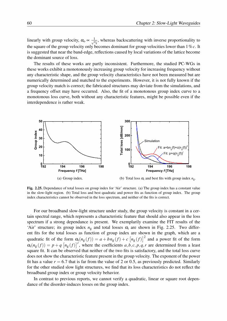
60 Chapter 2: Slow-Light Waveguides
linearly with group velocity, αo ∝ 1√vg, whereas backscattering with inverse proportionality to
the square of the group velocity only becomes dominant for group velocities lower than 1%c. Itis suggested that near the band-edge, reflections caused by local variations of the lattice becomethe dominant source of loss.
The results of these works are partly inconsistent. Furthermore, the studied PC-WGs inthese works exhibit a monotonously increasing group velocity for increasing frequency withoutany characteristic shape, and the group velocity characteristics have not been measured but arenumerically determined and matched to the experiments. However, it is not fully known if thegroup velocity match is correct; the fabricated structures may deviate from the simulations, anda frequency offset may have occurred. Also, the fit of a monotonous group index curve to amonotonous loss curve, both without any characteristic features, might be possible even if theinterdependence is rather weak.
192 194 196 1980
10
20
30
40
50
Gro
up in
dex
Frequency f [THz]
(a) Group index.
192 194 196 1980
100
200
300To
tal l
oss
[dB
/mm
]
Frequency f [THz]
Fit: a+bng(f)+c(ng(f))2
Fit: p+q(ng(f))r
Simulation
(b) Total loss αt and best fits with group index ng.
Fig. 2.25. Dependance of total losses on group index for ‘Air’ structure. (a) The group index has a constant valuein the slow-light region. (b) Total loss and best quadratic and power fits as function of group index. The groupindex characteristics cannot be observed in the loss spectrum, and neither of the fits is correct.
For our broadband slow-light structure under study, the group velocity is constant in a cer-tain spectral range, which represents a characteristic feature that should also appear in the lossspectrum if a strong dependance is present. We exemplarily examine the FIT results of the‘Air’ structure; its group index ng and total losses αt are shown in Fig. 2.25. Two differ-ent fits for the total losses as function of group index are shown in the graph, which are aquadratic fit of the form αt(ng ( f )) = a + bng ( f ) + c
[ng ( f )
]2 and a power fit of the formαt(ng ( f )) = p + q
[ng ( f )
]r, where the coefficients a,b,c, p,q,r are determined from a leastsquare fit. It can be observed that neither of the two fits is satisfactory, and the total loss curvedoes not show the characteristic feature present in the group velocity. The exponent of the powerfit has a value r = 6.7 that is far from the value of 2 or 0.5, as previously predicted. Similarlyfor the other studied slow light structures, we find that its loss characteristics do not reflect thebroadband group index or group velocity behavior.
In contrast to previous reports, we cannot verify a quadratic, linear or square root depen-dance of the disorder-induces losses on the group index.
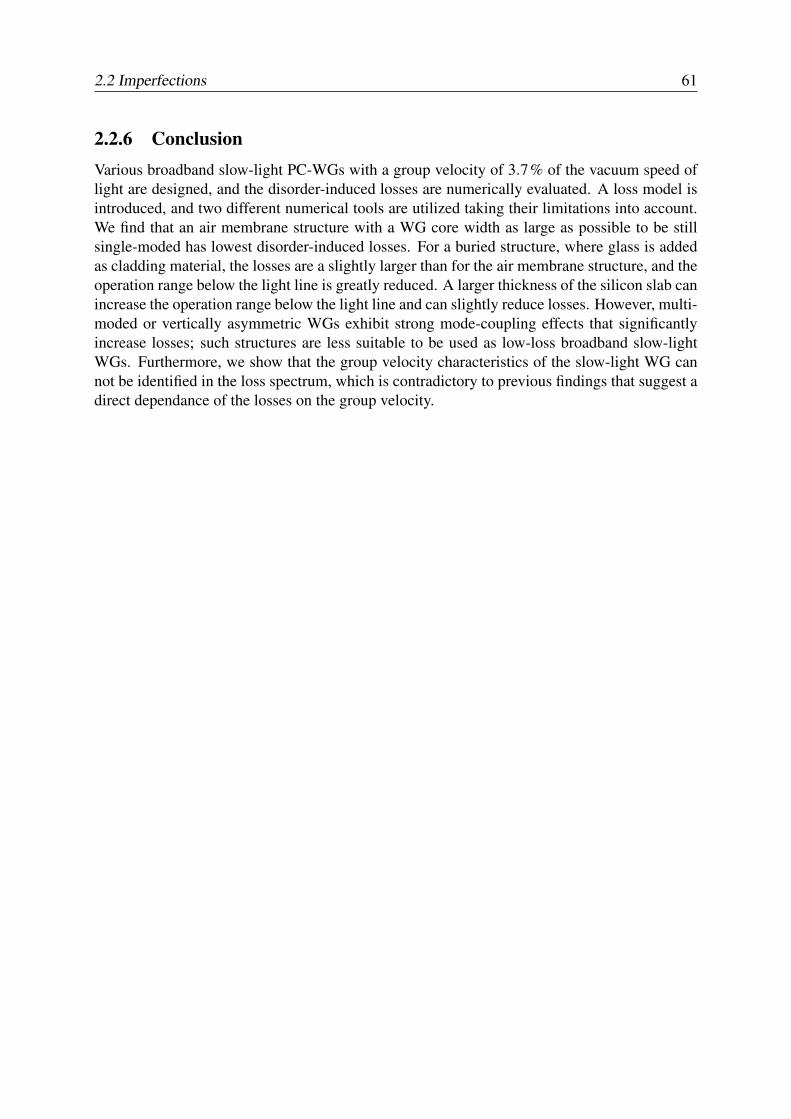
2.2 Imperfections 61
2.2.6 ConclusionVarious broadband slow-light PC-WGs with a group velocity of 3.7% of the vacuum speed oflight are designed, and the disorder-induced losses are numerically evaluated. A loss model isintroduced, and two different numerical tools are utilized taking their limitations into account.We find that an air membrane structure with a WG core width as large as possible to be stillsingle-moded has lowest disorder-induced losses. For a buried structure, where glass is addedas cladding material, the losses are a slightly larger than for the air membrane structure, and theoperation range below the light line is greatly reduced. A larger thickness of the silicon slab canincrease the operation range below the light line and can slightly reduce losses. However, multi-moded or vertically asymmetric WGs exhibit strong mode-coupling effects that significantlyincrease losses; such structures are less suitable to be used as low-loss broadband slow-lightWGs. Furthermore, we show that the group velocity characteristics of the slow-light WG cannot be identified in the loss spectrum, which is contradictory to previous findings that suggest adirect dependance of the losses on the group velocity.

62 Chapter 2: Slow-Light Waveguides
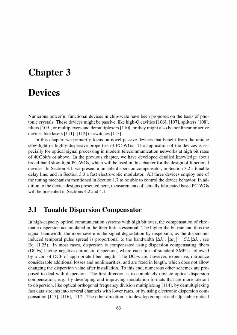
Chapter 3
Devices
Numerous powerful functional devices in chip-scale have been proposed on the basis of pho-tonic crystals. These devices might be passive, like high-Q cavities [106], [107], splitters [108],filters [109], or multiplexers and demultiplexers [110], or they might also be nonlinear or activedevices like lasers [111], [112] or switches [113].
In this chapter, we primarily focus on novel passive devices that benefit from the uniqueslow-light or highly-dispersive properties of PC-WGs. The application of the devices is es-pecially for optical signal processing in modern telecommunication networks at high bit ratesof 40Gbit/s or above. In the previous chapter, we have developed detailed knowledge aboutbroad-band slow-light PC-WGs, which will be used in this chapter for the design of functionaldevices. In Section 3.1, we present a tunable dispersion compensator, in Section 3.2 a tunabledelay line, and in Section 3.3 a fast electro-optic modulator. All three devices employ one ofthe tuning mechanism mentioned in Section 1.7 to be able to control the device behavior. In ad-dition to the device designs presented here, measurements of actually fabricated basic PC-WGswill be presented in Sections 4.2 and 4.1.
3.1 Tunable Dispersion Compensator
In high-capacity optical communication systems with high bit rates, the compensation of chro-matic dispersion accumulated in the fiber link is essential. The higher the bit rate and thus thesignal bandwidth, the more severe is the signal degradation by dispersion, as the dispersion-induced temporal pulse spread is proportional to the bandwidth |∆λ |,
∣∣∆tg∣∣ = C L |∆λ |, see
Eq. (1.25). In most cases, dispersion is compensated using dispersion compensating fibers(DCFs) having negative chromatic dispersion, where each link of standard SMF is followedby a coil of DCF of appropriate fiber length. The DCFs are, however, expensive, introduceconsiderable additional losses and nonlinearities, and are fixed in length, which does not allowchanging the dispersion value after installation. To this end, numerous other schemes are pro-posed to deal with dispersion. The first direction is to completely obviate optical dispersioncompensation, e. g. by developing and improving modulation formats that are more tolerantto dispersion, like optical orthogonal frequency division multiplexing [114], by demultiplexingfast data streams into several channels with lower rates, or by using electronic dispersion com-pensation [115], [116], [117]. The other direction is to develop compact and adjustable optical
63
64 Chapter 3: Devices
dispersion compensators, which can be realized by chirped fiber Bragg gratings [118], virtu-ally imaged phased arrays [119], all-pass multicavity etalons [120] or by all-pass filters basedon a micro-electro-mechanical system (MEMS) [121]. Furthermore, optical dispersion com-pensators can also be realized in integrated planar waveguide circuit, e. g. with coupled stripwaveguides [122], all-pass ring resonator filters [123], all-pass Mach-Zehnder interferometers[124], waveguide grating routers [125] or with phase-conjugating silicon waveguides [126].
Photonic crystals show in particular very strong dispersive properties: PC fibers exhibita much larger negative chromatic than standard DCFs [127], and integrated PC-WGs showregions of extremely high chromatic dispersion [14]. Based on such PC-WGs, compact devicesfor dispersion compensation have been suggested, [39], [128], [129].
In this section, we propose a tunable dispersion compensator based on two concatenatedPC-WGs that exhibits a flat dispersion in a wide 125GHz bandwidth. The dispersion canbe continuously tuned in a range between −19ps/(mmnm) and 7ps/(mmnm), and the to-tal length of the device determines the dispersion-length product and thus the dispersion thatcan be compensated. The device comprises two concatenated PC-WGs sections, where one ofthe sections has a linearly increasing chromatic dispersion characteristics as a function of fre-quency, while the other one has a linearly decreasing dispersion. The PC-WGs sections can bedesigned such that a flat total dispersion is obtained, and tuning one of the sections changes thedispersion value.
The section is organized as follows: In Subsection 3.1.1, the operation principle of thedevice is explained. In Subsection 3.1.2, details about the PC-WG design are shown, and inSubsection 3.1.3, simulation results of the complete device are presented indicating its feasibil-ity.
3.1.1 Principle of OperationThe total chromatic dispersion Ctot of two concatenated WG sections with chromatic dispersioncharacteristics C1,2 is calculated according to
Ctot =C1l1 +C2l2
l1 + l2, (3.1)
where the two sections have lengths l1,2. Multiplying the dispersion Ctot with the total lengthof the structure, Ltot = l1 + l2, the dispersion-length product CtotLtot is obtained, and obviouslyincreasing the total length Ltot of the device increases the dispersion that can be compensated,while the ratio of l1 and l2 needs to stay fixed in order to maintain the dispersion characteristics.
The tunable chromatic dispersion compensator is based on a PC-WG that is specificallydesigned to have a dispersion characteristics as shown in Fig. 3.1(a), which has already beenmentioned in Subsection 2.1.3. The chromatic dispersion characteristic exhibits a spectral re-gion with a linearly decreasing value, then the minimum dispersion is reached having a negativevalue, and a region with a linearly increasing dispersion follows. The linear dispersion regionsare marked by ovals in Fig. 3.1(a). A second section of PC-WG is introduced and is appropri-ately shifted in frequency by slightly changing the structure parameters, so that the regions oflinearly increasing and decreasing dispersion of sections 1 and 2 overlap, see Fig. 3.1(b). Theratio of the lengths of the two sections can be adjusted such that the dispersion-length products
3.1 Tunable Dispersion Compensator 65
193 194 195-40
-20
0
20
40
60
80Linearincrease
Lineardecrease
Dis
pers
ion
[ps
/ (m
m n
m)]
Frequency f [THz]
(a) Dispersion characteristics of PC-WG.
193 194 195 196-40
-20
0
20
40
60
80
Section 2
Dis
pers
ion
Len
gth
[ps
/ nm
]
Frequency f [THz]
Section 1
Overlapregion
(b) Dispersion-length product of PC-WG sections.
Fig. 3.1. Chromatic dispersion characteristics of PC-WG used for dispersion compensator. (a) The specificallydesigned PC-WG exhibits two spectral regions with linearly varying dispersion and negative minimum dispersion.(b) By concatenating two PC-WG sections of appropriate length and by frequency-shifting one of the sections, thetwo linear regions overlap and a flat total dispersion results.
in the overlap region have equal slopes but opposite sign, which means that the concatenationof the two sections results in a total dispersion characteristic with a nearly constant value ina considerable bandwidth. The schematic of the device structure is shown in Fig. 3.2, wherecoupling tapers have been introduced at the beginning and end of the PC-WGs to increase thetransmission, as explained in Subsection 2.1.4.
Fig. 3.2. Structure schematic of tunable dispersion compensator. Two sections of lengths l1 and l2 are concatenated,where section 1 is operated in the range of linearly increasing and section 2 of linearly decreasing dispersion. Ifsection 2 is tuned, its characteristics is shifted in frequency, and the resulting total dispersion can be varied. Toincrease the coupling to strip-WGs, PC tapers are introduced at both ends of the structure.
The resulting dispersion value of the device can now be made tunable by shifting the dis-persion characteristics of section 2 in frequency, which can be achieved with one of the tuningmechanisms introduced in Section 1.7, e. g. with free carrier injection or thermal tuning. The
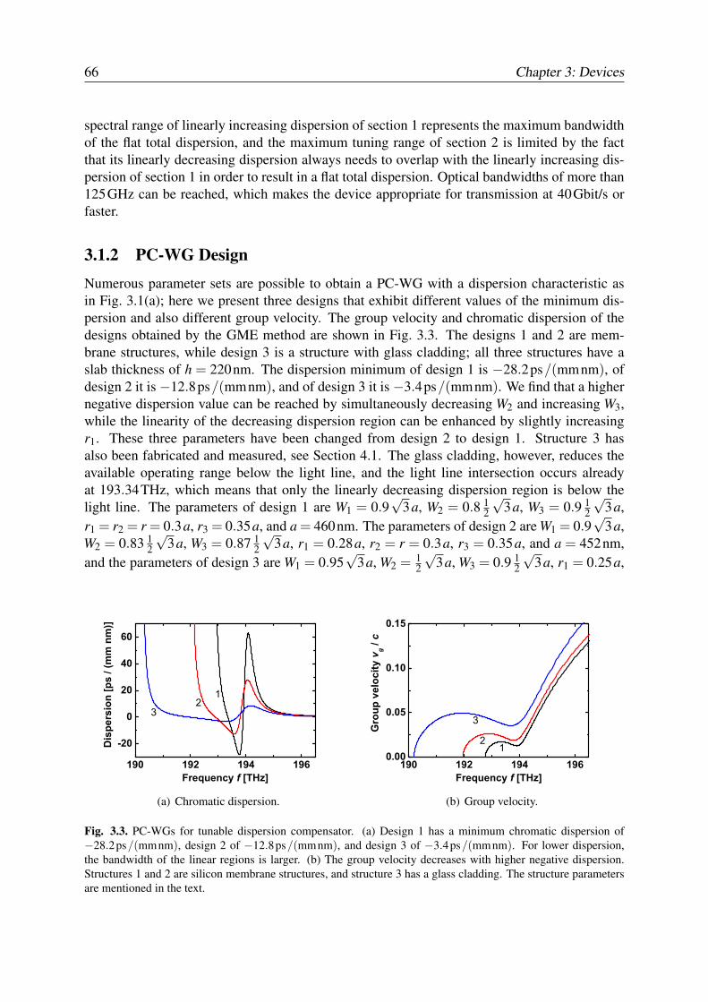
66 Chapter 3: Devices
spectral range of linearly increasing dispersion of section 1 represents the maximum bandwidthof the flat total dispersion, and the maximum tuning range of section 2 is limited by the factthat its linearly decreasing dispersion always needs to overlap with the linearly increasing dis-persion of section 1 in order to result in a flat total dispersion. Optical bandwidths of more than125GHz can be reached, which makes the device appropriate for transmission at 40Gbit/s orfaster.
3.1.2 PC-WG DesignNumerous parameter sets are possible to obtain a PC-WG with a dispersion characteristic asin Fig. 3.1(a); here we present three designs that exhibit different values of the minimum dis-persion and also different group velocity. The group velocity and chromatic dispersion of thedesigns obtained by the GME method are shown in Fig. 3.3. The designs 1 and 2 are mem-brane structures, while design 3 is a structure with glass cladding; all three structures have aslab thickness of h = 220nm. The dispersion minimum of design 1 is −28.2ps/(mmnm), ofdesign 2 it is −12.8ps/(mmnm), and of design 3 it is −3.4ps/(mmnm). We find that a highernegative dispersion value can be reached by simultaneously decreasing W2 and increasing W3,while the linearity of the decreasing dispersion region can be enhanced by slightly increasingr1. These three parameters have been changed from design 2 to design 1. Structure 3 hasalso been fabricated and measured, see Section 4.1. The glass cladding, however, reduces theavailable operating range below the light line, and the light line intersection occurs alreadyat 193.34THz, which means that only the linearly decreasing dispersion region is below thelight line. The parameters of design 1 are W1 = 0.9
√3a, W2 = 0.8 1
2
√3a, W3 = 0.9 1
2
√3a,
r1 = r2 = r = 0.3a, r3 = 0.35a, and a = 460nm. The parameters of design 2 are W1 = 0.9√
3a,W2 = 0.83 1
2
√3a, W3 = 0.87 1
2
√3a, r1 = 0.28a, r2 = r = 0.3a, r3 = 0.35a, and a = 452nm,
and the parameters of design 3 are W1 = 0.95√
3a, W2 = 12
√3a, W3 = 0.9 1
2
√3a, r1 = 0.25a,
190 192 194 196
-20
0
20
40
60
32
Dis
pers
ion
[ps
/ (m
m n
m)]
Frequency f [THz]
1
(a) Chromatic dispersion.
190 192 194 1960.00
0.05
0.10
0.15
3
21
Gro
up v
eloc
ity v
g / c
Frequency f [THz]
(b) Group velocity.
Fig. 3.3. PC-WGs for tunable dispersion compensator. (a) Design 1 has a minimum chromatic dispersion of−28.2ps/(mmnm), design 2 of −12.8ps/(mmnm), and design 3 of −3.4ps/(mmnm). For lower dispersion,the bandwidth of the linear regions is larger. (b) The group velocity decreases with higher negative dispersion.Structures 1 and 2 are silicon membrane structures, and structure 3 has a glass cladding. The structure parametersare mentioned in the text.
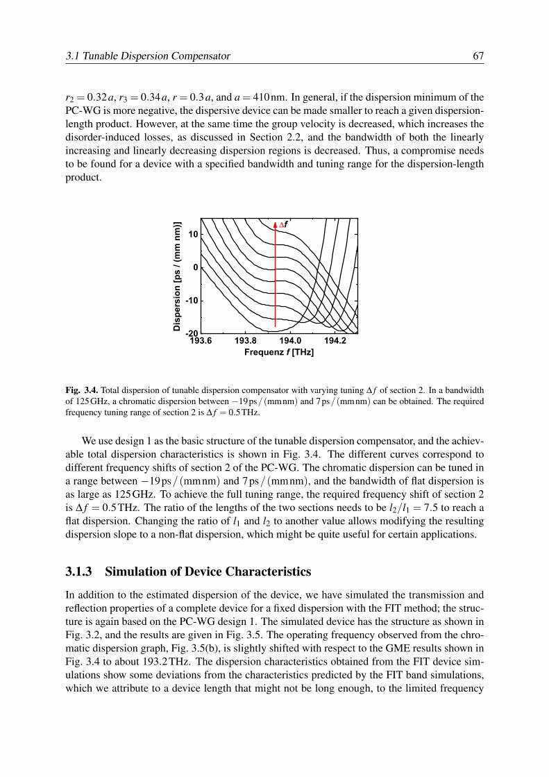
3.1 Tunable Dispersion Compensator 67
r2 = 0.32a, r3 = 0.34a, r = 0.3a, and a = 410nm. In general, if the dispersion minimum of thePC-WG is more negative, the dispersive device can be made smaller to reach a given dispersion-length product. However, at the same time the group velocity is decreased, which increases thedisorder-induced losses, as discussed in Section 2.2, and the bandwidth of both the linearlyincreasing and linearly decreasing dispersion regions is decreased. Thus, a compromise needsto be found for a device with a specified bandwidth and tuning range for the dispersion-lengthproduct.
193.6 193.8 194.0 194.2-20
-10
0
10
Dis
pers
ion
[ps
/ (m
m n
m)]
Frequenz f [THz]
f
Fig. 3.4. Total dispersion of tunable dispersion compensator with varying tuning ∆ f of section 2. In a bandwidthof 125GHz, a chromatic dispersion between −19ps/(mmnm) and 7ps/(mmnm) can be obtained. The requiredfrequency tuning range of section 2 is ∆ f = 0.5THz.
We use design 1 as the basic structure of the tunable dispersion compensator, and the achiev-able total dispersion characteristics is shown in Fig. 3.4. The different curves correspond todifferent frequency shifts of section 2 of the PC-WG. The chromatic dispersion can be tuned ina range between −19ps/(mmnm) and 7ps/(mmnm), and the bandwidth of flat dispersion isas large as 125GHz. To achieve the full tuning range, the required frequency shift of section 2is ∆ f = 0.5THz. The ratio of the lengths of the two sections needs to be l2/l1 = 7.5 to reach aflat dispersion. Changing the ratio of l1 and l2 to another value allows modifying the resultingdispersion slope to a non-flat dispersion, which might be quite useful for certain applications.
3.1.3 Simulation of Device Characteristics
In addition to the estimated dispersion of the device, we have simulated the transmission andreflection properties of a complete device for a fixed dispersion with the FIT method; the struc-ture is again based on the PC-WG design 1. The simulated device has the structure as shown inFig. 3.2, and the results are given in Fig. 3.5. The operating frequency observed from the chro-matic dispersion graph, Fig. 3.5(b), is slightly shifted with respect to the GME results shown inFig. 3.4 to about 193.2THz. The dispersion characteristics obtained from the FIT device sim-ulations show some deviations from the characteristics predicted by the FIT band simulations,which we attribute to a device length that might not be long enough, to the limited frequency
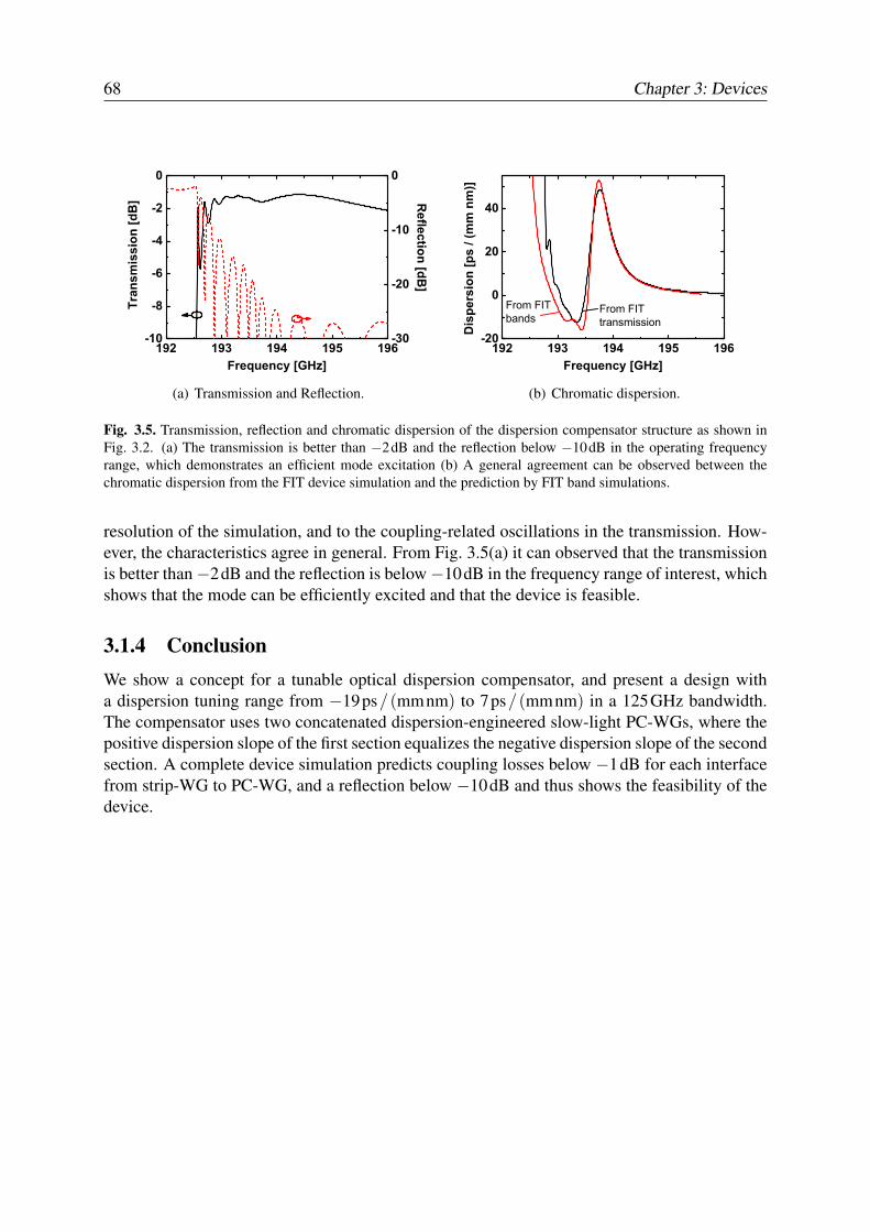
68 Chapter 3: Devices
192 193 194 195 196-10
-8
-6
-4
-2
0
-30
-20
-10
0
Tran
smis
sion
[dB
]
Frequency [GHz]
Reflection [dB
]
(a) Transmission and Reflection.
192 193 194 195 196-20
0
20
40
From FITtransmission
Dis
pers
ion
[ps
/ (m
m n
m)]
Frequency [GHz]
From FITbands
(b) Chromatic dispersion.
Fig. 3.5. Transmission, reflection and chromatic dispersion of the dispersion compensator structure as shown inFig. 3.2. (a) The transmission is better than −2dB and the reflection below −10dB in the operating frequencyrange, which demonstrates an efficient mode excitation (b) A general agreement can be observed between thechromatic dispersion from the FIT device simulation and the prediction by FIT band simulations.
resolution of the simulation, and to the coupling-related oscillations in the transmission. How-ever, the characteristics agree in general. From Fig. 3.5(a) it can observed that the transmissionis better than−2dB and the reflection is below−10dB in the frequency range of interest, whichshows that the mode can be efficiently excited and that the device is feasible.
3.1.4 ConclusionWe show a concept for a tunable optical dispersion compensator, and present a design witha dispersion tuning range from −19ps/(mmnm) to 7ps/(mmnm) in a 125GHz bandwidth.The compensator uses two concatenated dispersion-engineered slow-light PC-WGs, where thepositive dispersion slope of the first section equalizes the negative dispersion slope of the secondsection. A complete device simulation predicts coupling losses below −1dB for each interfacefrom strip-WG to PC-WG, and a reflection below −10dB and thus shows the feasibility of thedevice.

3.2 Tunable Optical Delay Line 69
3.2 Tunable Optical Delay LineIn next-generation all-optical networks, tunable optical delay lines might play an importantrole for optical buffering, data synchronization, optical memory and optical signal processing.Furthermore, tunable optical delays are also needed in metrology e. g. for LIDAR (Light De-tection and Ranging) or RADAR (Radio Detection and Ranging) applications. The requireddevice bandwidth in fast communication system is in the order of twice the transmitted bit rate,and for 40Gbit/s transmission an optical bandwidth of 125GHz is safe. Bandwidths of thisorder of magnitude cannot be reached using electromagnetically induced transparency (EIT).By using coherent population oscillation (CPO) in a semiconductor, a maximally tunable delayof 2ps corresponding to 0.07 pulsewidths was shown at 16.7GHz modulation [76]. By usingstimulated Brillouin scattering (SBS), data with a rate of 14Gbit/s could be delayed up to 0.62pulsewidths [130]. With stimulated Raman scattering (SRS), an optical signal of a bandwidth ashigh as 1THz was delayed by 0.85 pulsewidths [79]. Much higher delays can be achieved usingself-phase modulation and dispersion, where a 10Gbit/s data signal was continuously delayedup to 45 pulsewidths, and maximum data rates of 60Gbit/s [131] are possible in principle. Inintegrated optical ring resonators, a 20Gbit/s optical signal was delayed by a fixed amount of10 bits [85], and a 2.5Gbit/s signal was delayed up to 2 bits [132].
In this section, we suggest a tunable optical delay line based on a silicon slow-light pho-tonic crystal. The device is designed to have a bandwidth of constant delay of 125GHz, anda 40Gbit/s 33% RZ signal can be continuously delayed from 0 to 5 pulsewidths on a devicelength of 1mm only. The principle of operation is similar to that of the tunable dispersion com-pensator presented in Section 3.1. Two sections of PC-WG are concatenated, where one sectionexhibits a positive flat chromatic dispersion and the other section a negative flat dispersion. Theresulting group delay is constant in a certain bandwidth, and by tuning one of the sections thetotal delay can be changed.
This section is organized as follows: In Subsection 3.2.1, the device principle is explainedin more detail, followed by PC-WG design considerations in Subsection 3.2.2. An optimizationstrategy is presented in Subsection 3.2.3, and the tunable delay characteristics are estimated.
3.2.1 Principle of OperationThe group delay tg in a device or waveguide of length L is related to the group index ng and tothe group velocity vg by the following equations:
tg = L1vg
(3.2)
= Lng
c, (3.3)
where c is the vacuum speed of light. The total group delay tg, tot of two different concatenatedWG section with group delays tg1, 2 or group indices ng1, 2 and lengths l1,2 is calculated by
tg, tot = tg1 + tg2 (3.4)
= l1ng1
c+ l2
ng2
c, (3.5)
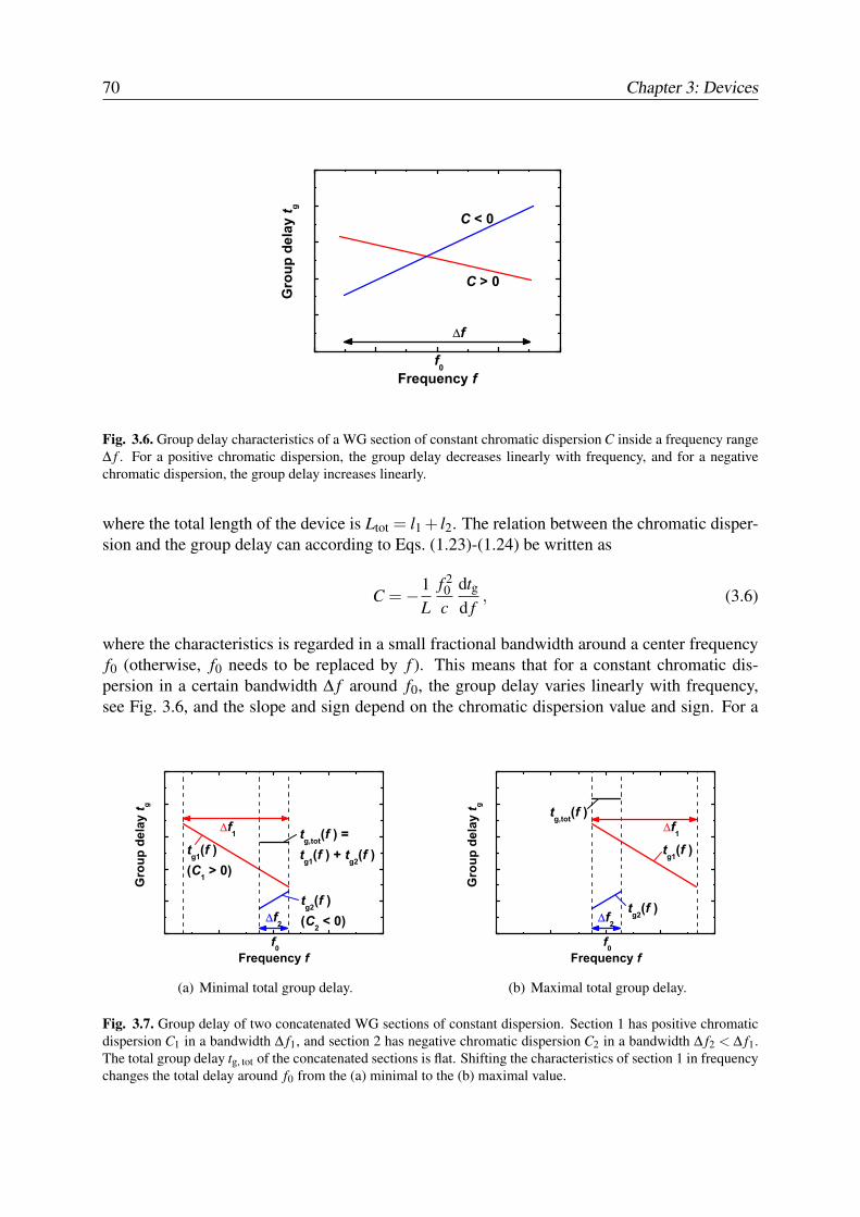
70 Chapter 3: Devices
f
C < 0
Gro
up d
elay
t g
Frequency ff0
C > 0
Fig. 3.6. Group delay characteristics of a WG section of constant chromatic dispersion C inside a frequency range∆ f . For a positive chromatic dispersion, the group delay decreases linearly with frequency, and for a negativechromatic dispersion, the group delay increases linearly.
where the total length of the device is Ltot = l1 + l2. The relation between the chromatic disper-sion and the group delay can according to Eqs. (1.23)-(1.24) be written as
C =−1L
f 20c
dtgd f
, (3.6)
where the characteristics is regarded in a small fractional bandwidth around a center frequencyf0 (otherwise, f0 needs to be replaced by f ). This means that for a constant chromatic dis-persion in a certain bandwidth ∆ f around f0, the group delay varies linearly with frequency,see Fig. 3.6, and the slope and sign depend on the chromatic dispersion value and sign. For a
tg,tot(f ) =tg1(f ) + tg2(f )
tg1(f )(C1 > 0)
f2
tg2(f )(C2 < 0)
Gro
up d
elay
t g
Frequency ff0
f1
(a) Minimal total group delay.
tg,tot(f )
tg1(f )
f2
tg2(f )
Gro
up d
elay
t g
Frequency ff0
f1
(b) Maximal total group delay.
Fig. 3.7. Group delay of two concatenated WG sections of constant dispersion. Section 1 has positive chromaticdispersion C1 in a bandwidth ∆ f1, and section 2 has negative chromatic dispersion C2 in a bandwidth ∆ f2 < ∆ f1.The total group delay tg, tot of the concatenated sections is flat. Shifting the characteristics of section 1 in frequencychanges the total delay around f0 from the (a) minimal to the (b) maximal value.
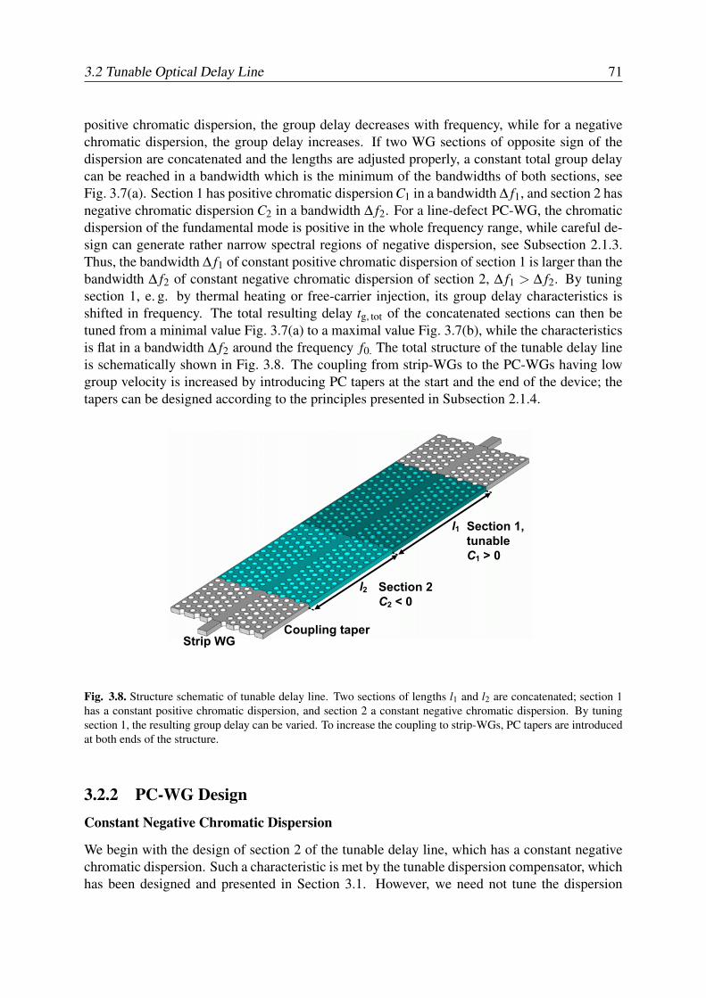
3.2 Tunable Optical Delay Line 71
positive chromatic dispersion, the group delay decreases with frequency, while for a negativechromatic dispersion, the group delay increases. If two WG sections of opposite sign of thedispersion are concatenated and the lengths are adjusted properly, a constant total group delaycan be reached in a bandwidth which is the minimum of the bandwidths of both sections, seeFig. 3.7(a). Section 1 has positive chromatic dispersion C1 in a bandwidth ∆ f1, and section 2 hasnegative chromatic dispersion C2 in a bandwidth ∆ f2. For a line-defect PC-WG, the chromaticdispersion of the fundamental mode is positive in the whole frequency range, while careful de-sign can generate rather narrow spectral regions of negative dispersion, see Subsection 2.1.3.Thus, the bandwidth ∆ f1 of constant positive chromatic dispersion of section 1 is larger than thebandwidth ∆ f2 of constant negative chromatic dispersion of section 2, ∆ f1 > ∆ f2. By tuningsection 1, e. g. by thermal heating or free-carrier injection, its group delay characteristics isshifted in frequency. The total resulting delay tg, tot of the concatenated sections can then betuned from a minimal value Fig. 3.7(a) to a maximal value Fig. 3.7(b), while the characteristicsis flat in a bandwidth ∆ f2 around the frequency f0. The total structure of the tunable delay lineis schematically shown in Fig. 3.8. The coupling from strip-WGs to the PC-WGs having lowgroup velocity is increased by introducing PC tapers at the start and the end of the device; thetapers can be designed according to the principles presented in Subsection 2.1.4.
C2
C1 >
l2
l1
Fig. 3.8. Structure schematic of tunable delay line. Two sections of lengths l1 and l2 are concatenated; section 1has a constant positive chromatic dispersion, and section 2 a constant negative chromatic dispersion. By tuningsection 1, the resulting group delay can be varied. To increase the coupling to strip-WGs, PC tapers are introducedat both ends of the structure.
3.2.2 PC-WG DesignConstant Negative Chromatic Dispersion
We begin with the design of section 2 of the tunable delay line, which has a constant negativechromatic dispersion. Such a characteristic is met by the tunable dispersion compensator, whichhas been designed and presented in Section 3.1. However, we need not tune the dispersion
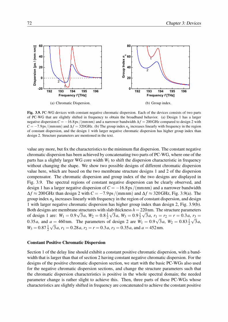
72 Chapter 3: Devices
192 193 194 195 196-20
0
20
40
60
2
Dis
pers
ion
[ps
/ (m
m n
m)]
Frequency f [THz]
1
(a) Chromatic Dispersion.
192 193 194 195 1960
20
40
60
80
Gro
up In
dex n g
Frequency f [THz]
1
2
(b) Group index.
Fig. 3.9. PC-WG devices with constant negative chromatic dispersion. Each of the devices consists of two partsof PC-WG that are slightly shifted in frequency to obtain the broadband behavior. (a) Design 1 has a largernegative dispersion C =−16.8ps/(mmnm) and a narrower bandwidth ∆ f = 200GHz compared to design 2 withC =−7.9ps/(mmnm) and ∆ f = 320GHz. (b) The group index ng increases linearly with frequency in the regionof constant dispersion, and the design 1 with larger negative chromatic dispersion has higher group index thandesign 2. Structure parameters are mentioned in the text.
value any more, but fix the characteristics to the minimum flat dispersion. The constant negativechromatic dispersion has been achieved by concatenating two parts of PC-WG, where one of theparts has a slightly larger WG core width W1 to shift the dispersion characteristic in frequencywithout changing the shape. We show two possible designs of different chromatic dispersionvalue here, which are based on the two membrane structure designs 1 and 2 of the dispersioncompensator. The chromatic dispersion and group index of the two designs are displayed inFig. 3.9. The spectral regions of constant negative dispersion can be clearly observed, anddesign 1 has a larger negative dispersion of C =−16.8ps/(mmnm) and a narrower bandwidth∆ f ≈ 200GHz than design 2 with C =−7.9ps/(mmnm) and ∆ f ≈ 320GHz, Fig. 3.9(a). Thegroup index ng increases linearly with frequency in the region of constant dispersion, and design1 with larger negative chromatic dispersion has higher group index than design 2, Fig. 3.9(b).Both designs are membrane structures with slab thickness h = 220nm. The structure parametersof design 1 are: W1 = 0.9
√3a, W2 = 0.8 1
2
√3a, W3 = 0.9 1
2
√3a, r1 = r2 = r = 0.3a, r3 =
0.35a, and a = 460nm. The parameters of design 2 are W1 = 0.9√
3a, W2 = 0.83 12
√3a,
W3 = 0.87 12
√3a, r1 = 0.28a, r2 = r = 0.3a, r3 = 0.35a, and a = 452nm.
Constant Positive Chromatic Dispersion
Section 1 of the delay line should exhibit a constant positive chromatic dispersion, with a band-width that is larger than that of section 2 having constant negative chromatic dispersion. For thedesigns of the positive chromatic dispersion section, we start with the basic PC-WGs also usedfor the negative chromatic dispersion sections, and change the structure parameters such thatthe chromatic dispersion characteristics is positive in the whole spectral domain; the neededparameter change is rather slight to achieve this. Then, three parts of these PC-WGs whosecharacteristics are slightly shifted in frequency are concatenated to achieve the constant positive

3.2 Tunable Optical Delay Line 73
191 192 193 194 195 1960
2
4
6
8
10
C1l1 = Cp1lp1 + Cp2lp2 + Cp3lp3
Cp2lp2
Cp3lp3
Cp1lp1
Dis
pers
ion
Len
gth
[ps
/ nm
]
Frequency f [THz]
Fig. 3.10. Principle to obtain constant positive chromatic dispersion. A flat dispersion characteristic C1l1 can beobtained by concatenating three parts of PC-WG each having positive chromatic dispersion characteristics withslight frequency shifts against each other. The required frequency shifts and lengths of the three parts are foundwith a parameter fit.
dispersion in a large bandwidth. The resulting dispersion-length product of the section (section1) C1l1 is just the sum of the dispersion-length products of the three parts Cp1, 2, 3 lp1, 2, 3; thisis expressed by C1l1 = Cp1lp1 +Cp3lp3 +Cp3lp3. The principle is displayed in Fig. 3.10. Theshift of the dispersion characteristics in frequency can again be achieved by slightly chang-ing the core width W1 of the WG. The optimum frequency shifts and lengths of the parts aredetermined by using a parameter fit. In general, also more than three WG parts can be used,or parameters can be continuously varied over the WG length, which results in a even flatterdispersion characteristics.
In Fig. 3.11, the chromatic dispersion and group index of the two designs are shown, wheredesign 2 is that as already presented previously in Fig. 3.10 with l1 = 1mm. Design 1 has,similarly to the designs for negative chromatic dispersion, a larger positive chromatic dis-persion C ≈ 14.6ps/(mmnm) and a narrower bandwidth ∆ f ≈ 800GHz than design 2 withC = 6.6ps/(mmnm) and ∆ f ≈ 1,200GHz, Fig. 3.11(a). The group index ng decreases linearlywith frequency in the region of constant dispersion, and design 1 exhibiting larger chromatic dis-persion has higher group index than design 2, Fig. 3.9(b). In comparison to the designs for neg-ative chromatic dispersion, only the parameters r2 and r3 have been changed. For completeness,we repeat all structure parameters here. The membrane slab thickness is h = 220nm. Design 1has the following parameters: W1 = 0.9
√3a, W2 = 0.8 1
2
√3a, W3 = 0.9 1
2
√3a, r1 = r = 0.3a,
r2 = 0.28a, r3 = 0.34a, and a = 460nm. The parameters of design 2 are W1 = 0.9√
3a, W2 =0.83 1
2
√3a, W3 = 0.87 1
2
√3a, r1 = 0.28a, r2 = 0.27a, r3 = 0.33a, r = 0.3a and a = 452nm.
3.2.3 Optimization
For a tunable delay line, the tuning range of the group delay ∆tg is the most relevant parameter,while the bandwidth should be sufficiently large for fast optical signals. Our aim is to obtain abandwidth of 125GHz, which allows transmission of at least 40Gbit/s signals. As mentioned in
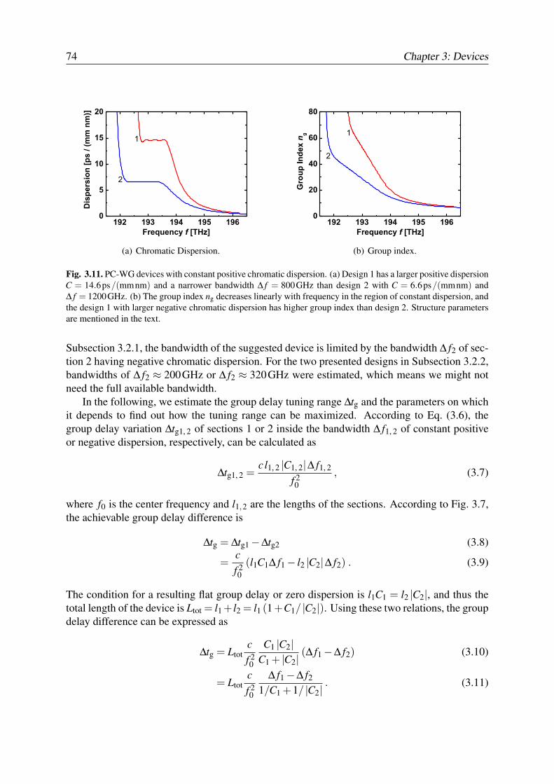
74 Chapter 3: Devices
192 193 194 195 1960
5
10
15
20
2
1
Dis
pers
ion
[ps
/ (m
m n
m)]
Frequency f [THz]
(a) Chromatic Dispersion.
192 193 194 195 1960
20
40
60
80
1
2
Gro
up In
dex n g
Frequency f [THz]
(b) Group index.
Fig. 3.11. PC-WG devices with constant positive chromatic dispersion. (a) Design 1 has a larger positive dispersionC = 14.6ps/(mmnm) and a narrower bandwidth ∆ f = 800GHz than design 2 with C = 6.6ps/(mmnm) and∆ f = 1200GHz. (b) The group index ng decreases linearly with frequency in the region of constant dispersion, andthe design 1 with larger negative chromatic dispersion has higher group index than design 2. Structure parametersare mentioned in the text.
Subsection 3.2.1, the bandwidth of the suggested device is limited by the bandwidth ∆ f2 of sec-tion 2 having negative chromatic dispersion. For the two presented designs in Subsection 3.2.2,bandwidths of ∆ f2 ≈ 200GHz or ∆ f2 ≈ 320GHz were estimated, which means we might notneed the full available bandwidth.
In the following, we estimate the group delay tuning range ∆tg and the parameters on whichit depends to find out how the tuning range can be maximized. According to Eq. (3.6), thegroup delay variation ∆tg1, 2 of sections 1 or 2 inside the bandwidth ∆ f1, 2 of constant positiveor negative dispersion, respectively, can be calculated as
∆tg1, 2 =c l1, 2 |C1, 2|∆ f1, 2
f 20
, (3.7)
where f0 is the center frequency and l1,2 are the lengths of the sections. According to Fig. 3.7,the achievable group delay difference is
∆tg = ∆tg1−∆tg2 (3.8)
=cf 20
(l1C1∆ f1− l2 |C2|∆ f2) . (3.9)
The condition for a resulting flat group delay or zero dispersion is l1C1 = l2 |C2|, and thus thetotal length of the device is Ltot = l1 + l2 = l1 (1+C1/ |C2|). Using these two relations, the groupdelay difference can be expressed as
∆tg = Ltotcf 20
C1 |C2|C1 + |C2|
(∆ f1−∆ f2) (3.10)
= Ltotcf 20
∆ f1−∆ f2
1/C1 +1/ |C2|. (3.11)
3.2 Tunable Optical Delay Line 75
Clearly, the group delay tuning range can for fixed length Ltot be maximized by maximizingboth dispersion values C1 and |C2|, and by maximizing the bandwidth difference ∆ f1−∆ f2.Thus, even if the available bandwidth ∆ f2 might be larger than required, we would choose onlythe minimum needed, in our case ∆ f2 = 125GHz. For the two designs of constant positive andnegative dispersion presented above in Subsection 3.2.2, the magnitude of the dispersion valueshas been maximized. It needs to be mentioned, however, that the magnitude of the chromaticdispersion can in practice not be arbitrarily increased, as the group velocity decreases simulta-neously in the PC-WG and losses are thus increased; this might become the major limitationfor the device.
For the two presented designs, the group delay difference for devices with a total length of1mm can be calculated, where we fix ∆ f1 = 125GHz. For design 1 with C1 = 14.6ps/(mmnm),∆ f1 = 800GHz and C2 =−16.8ps/(mmnm), we obtain ∆tg = 42.2ps. This corresponds to 5.1pulsewidths for a 40Gbit/s 33% RZ data signal. The length ratio of the two sections is l1/l2 =1.15. For design 2 with C1 = 6.6ps/(mmnm), ∆ f1 = 1,200GHz and C2 =−7.9ps/(mmnm),the tunable delay is ∆tg = 31.0ps corresponding to 3.8 pulsewidths of a 40Gbit/s 33% RZ datasignal; the length ratio is for that case l1/l2 = 1.20.
Clearly, if the length of the delay line is increased, also the delay range can be increased.In principle, much higher data rates than 40Gbit/s can be transmitted if the optical bandwidthof 125GHz is fully exploited or the bandwidth ∆ f2 is even further increased to the maximalpossible value, or if a modulation format is used that is spectrally more efficient.
3.2.4 ConclusionWe present a tunable delay line with a group delay tuning range of 42.2ps in a 125GHz op-tical bandwidth, while the device length is only 1mm. The delay range corresponds to 5.1pulsewidths of a 40Gbit/s 33% RZ data signal, and even higher bit rates are possible withthe given optical bandwidth. The delay line is realized by two concatenated PC-WGs havingconstant dispersion values of opposite sign.

76 Chapter 3: Devices

3.3 Compact High-Speed Electro-Optic Modulator 77
3.3 Compact High-Speed Electro-Optic ModulatorFast Mach-Zehnder silicon modulators with low operating voltage fabricated in CMOS tech-nology have the potential to considerably cut costs for high-speed optical transceivers. So far,the fastest broadband light modulation in silicon technology was achieved with free-carrierinjection, which allowed modulation up to 30GHz [133]. On the other hand, much higher mod-ulation frequencies can be achieved with organic materials through the virtually instantaneouselectro-optic effect. And indeed, modulation at 165GHz has been shown in a polymer ringresonator [134], however for a signal bandwidth of a few GHz only. Besides providing a fastelectro-optic effect, organic materials have a few more advantages. Poled organic materials canhave electro-optic coefficients ranging from moderate r33 = 10pm/V [135] to extremely highvalues of r33 = 170pm/V [65], [136], thus enabling operation with low drive voltage. Further,the organic materials can be infiltrated into silicon structures [17], [137]. This allows combiningthe highly nonlinear characteristics of the organic materials with the good high-index guidingproperties of silicon-on-insulator devices. To reduce even further the structure size, the drivevoltage, and the electrical power dissipation of silicon-organic based modulators, resonant ele-ments [138], [139], [140] or photonic crystals with low group velocity [61] may be employed.
In this section we propose an ultra-compact silicon-based Mach-Zehnder amplitude modu-lator with a 78GHz modulation bandwidth and a drive voltage of 1V, which allows data trans-mission at 100Gbit/s. This is achieved by infiltrating an electro-optic organic materials into aslotted photonic crystal waveguide, thereby making use of the fast electro-optic effects of or-ganic materials, the strong field confinement in slotted waveguides and the slow light interactionenhancements provided by the photonic crystal waveguide, where group velocity and dispersionmay be controlled [14], Subsection 2.1.3.
This section is organized as follows: In Subsection 3.3.1, we introduce the Mach-Zehndermodulator. Subsection 3.3.2 explains the optimization strategy. Subsection 3.3.3 gives detailsof the slow-wave phase modulator design. In Subsection 3.3.4, modulator parameters like mod-ulation bandwidth and π-voltage are discussed. Subsection 3.3.5 is devoted to performancedata of an optimized integratable Mach-Zehnder modulator, and in Subsection 3.3.6 a taper isproposed for coupling efficiently to the slow-light mode of the phase modulator sections. TheAppendix A.7 gives derivations of important relations.
The contents of this section have been published in a journal article, [1] or [J3] on page 165.
3.3.1 The Modulator
The configuration of the integrated Mach-Zehnder (MZ) interferometer (MZI) modulator(MZM) in silicon-on-insulator (SOI) technology is shown schematically in Fig. 3.12. The op-tical strip waveguides are operated in quasi-TE mode, where the optical field has a dominantelectric field component Ex oriented parallel to the substrate plane. Y-branches split and com-bine the signals. Both arms of the MZ interferometer comprise phase modulator (PM) sectionsof length L. The PM sections consist of photonic crystal (PC) line defect waveguides (WGs)with a narrow gap of width Wgap in the center, and are infiltrated with a χ(2)-nonlinear material(Pockels effect). In such a PC-WG, the dominant optical field component Ex is strongly con-fined to the gap (see Subsection 3.3.3). The nonlinear material is assumed to be poled [136]such that the axis of strongest electro-optic interaction (arrow ⇑ in Fig. 3.12) is aligned along
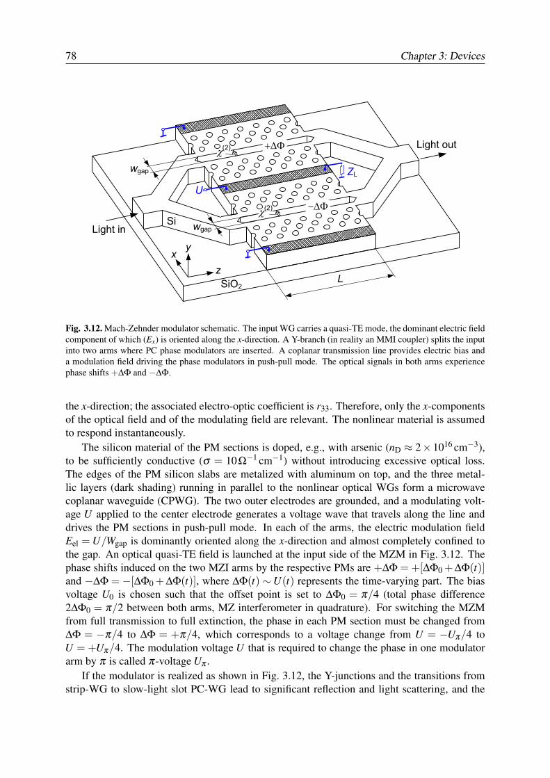
78 Chapter 3: Devices
Fig. 3.12. Mach-Zehnder modulator schematic. The input WG carries a quasi-TE mode, the dominant electric fieldcomponent of which (Ex) is oriented along the x-direction. A Y-branch (in reality an MMI coupler) splits the inputinto two arms where PC phase modulators are inserted. A coplanar transmission line provides electric bias anda modulation field driving the phase modulators in push-pull mode. The optical signals in both arms experiencephase shifts +∆Φ and −∆Φ.
the x-direction; the associated electro-optic coefficient is r33. Therefore, only the x-componentsof the optical field and of the modulating field are relevant. The nonlinear material is assumedto respond instantaneously.
The silicon material of the PM sections is doped, e.g., with arsenic (nD ≈ 2× 1016 cm−3),to be sufficiently conductive (σ = 10Ω−1 cm−1) without introducing excessive optical loss.The edges of the PM silicon slabs are metalized with aluminum on top, and the three metal-lic layers (dark shading) running in parallel to the nonlinear optical WGs form a microwavecoplanar waveguide (CPWG). The two outer electrodes are grounded, and a modulating volt-age U applied to the center electrode generates a voltage wave that travels along the line anddrives the PM sections in push-pull mode. In each of the arms, the electric modulation fieldEel = U/Wgap is dominantly oriented along the x-direction and almost completely confined tothe gap. An optical quasi-TE field is launched at the input side of the MZM in Fig. 3.12. Thephase shifts induced on the two MZI arms by the respective PMs are +∆Φ = +[∆Φ0 +∆Φ(t)]and −∆Φ = −[∆Φ0 + ∆Φ(t)], where ∆Φ(t) ∼U(t) represents the time-varying part. The biasvoltage U0 is chosen such that the offset point is set to ∆Φ0 = π/4 (total phase difference2∆Φ0 = π/2 between both arms, MZ interferometer in quadrature). For switching the MZMfrom full transmission to full extinction, the phase in each PM section must be changed from∆Φ = −π/4 to ∆Φ = +π/4, which corresponds to a voltage change from U = −Uπ/4 toU = +Uπ/4. The modulation voltage U that is required to change the phase in one modulatorarm by π is called π-voltage Uπ .
If the modulator is realized as shown in Fig. 3.12, the Y-junctions and the transitions fromstrip-WG to slow-light slot PC-WG lead to significant reflection and light scattering, and the
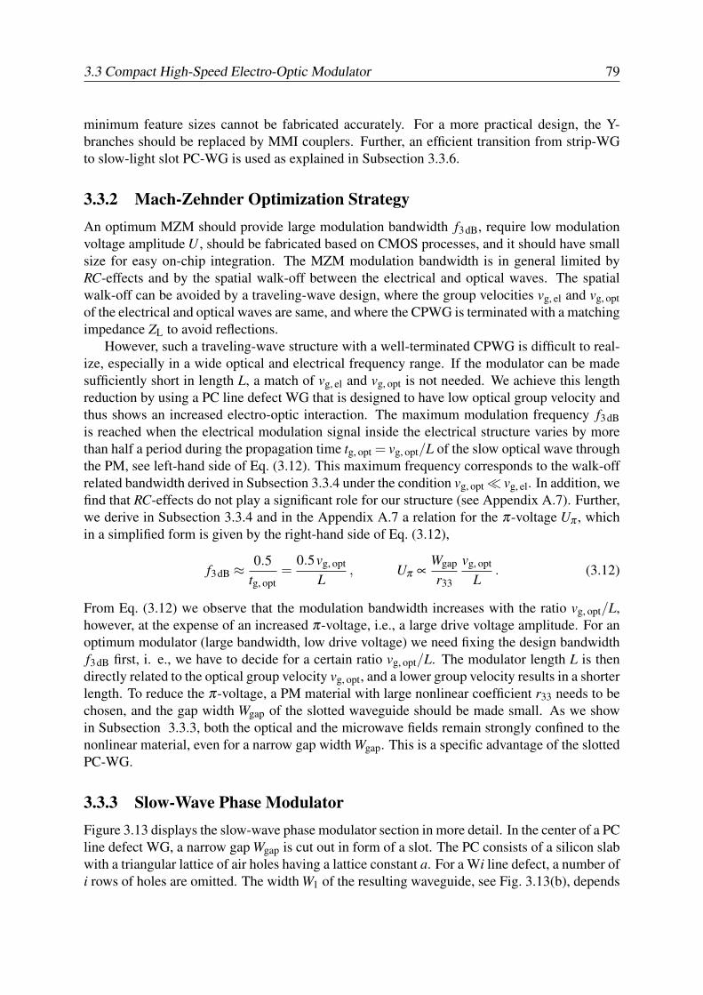
3.3 Compact High-Speed Electro-Optic Modulator 79
minimum feature sizes cannot be fabricated accurately. For a more practical design, the Y-branches should be replaced by MMI couplers. Further, an efficient transition from strip-WGto slow-light slot PC-WG is used as explained in Subsection 3.3.6.
3.3.2 Mach-Zehnder Optimization StrategyAn optimum MZM should provide large modulation bandwidth f3dB, require low modulationvoltage amplitude U , should be fabricated based on CMOS processes, and it should have smallsize for easy on-chip integration. The MZM modulation bandwidth is in general limited byRC-effects and by the spatial walk-off between the electrical and optical waves. The spatialwalk-off can be avoided by a traveling-wave design, where the group velocities vg, el and vg, optof the electrical and optical waves are same, and where the CPWG is terminated with a matchingimpedance ZL to avoid reflections.
However, such a traveling-wave structure with a well-terminated CPWG is difficult to real-ize, especially in a wide optical and electrical frequency range. If the modulator can be madesufficiently short in length L, a match of vg, el and vg, opt is not needed. We achieve this lengthreduction by using a PC line defect WG that is designed to have low optical group velocity andthus shows an increased electro-optic interaction. The maximum modulation frequency f3dBis reached when the electrical modulation signal inside the electrical structure varies by morethan half a period during the propagation time tg, opt = vg, opt/L of the slow optical wave throughthe PM, see left-hand side of Eq. (3.12). This maximum frequency corresponds to the walk-offrelated bandwidth derived in Subsection 3.3.4 under the condition vg, opt ¿ vg, el. In addition, wefind that RC-effects do not play a significant role for our structure (see Appendix A.7). Further,we derive in Subsection 3.3.4 and in the Appendix A.7 a relation for the π-voltage Uπ , whichin a simplified form is given by the right-hand side of Eq. (3.12),
f3dB ≈ 0.5tg, opt
=0.5vg, opt
L, Uπ ∝
Wgap
r33
vg, opt
L. (3.12)
From Eq. (3.12) we observe that the modulation bandwidth increases with the ratio vg, opt/L,however, at the expense of an increased π-voltage, i.e., a large drive voltage amplitude. For anoptimum modulator (large bandwidth, low drive voltage) we need fixing the design bandwidthf3dB first, i. e., we have to decide for a certain ratio vg, opt/L. The modulator length L is thendirectly related to the optical group velocity vg, opt, and a lower group velocity results in a shorterlength. To reduce the π-voltage, a PM material with large nonlinear coefficient r33 needs to bechosen, and the gap width Wgap of the slotted waveguide should be made small. As we showin Subsection 3.3.3, both the optical and the microwave fields remain strongly confined to thenonlinear material, even for a narrow gap width Wgap. This is a specific advantage of the slottedPC-WG.
3.3.3 Slow-Wave Phase ModulatorFigure 3.13 displays the slow-wave phase modulator section in more detail. In the center of a PCline defect WG, a narrow gap Wgap is cut out in form of a slot. The PC consists of a silicon slabwith a triangular lattice of air holes having a lattice constant a. For a Wi line defect, a number ofi rows of holes are omitted. The width W1 of the resulting waveguide, see Fig. 3.13(b), depends
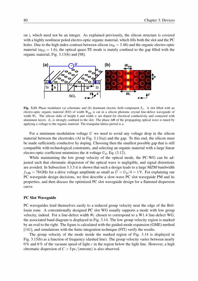
80 Chapter 3: Devices
on i, which need not be an integer. As explained previously, the silicon structure is coveredwith a highly nonlinear poled electro-optic organic material, which fills both the slot and the PCholes. Due to the high index-contrast between silicon (nSi = 3.48) and the organic electro-opticmaterial (nEO = 1.6), the optical quasi-TE mode is mainly confined to the gap filled with theorganic material, Fig. 3.13(b) and [98].
Fig. 3.13. Phase modulator (a) schematic and (b) dominant electric field component Ex. A slot filled with anelectro-optic organic material (EO) of width Wgap is cut in a silicon photonic crystal line-defect waveguide ofwidth W1. The silicon slabs of height h and width w are doped for electrical conductivity and contacted withaluminum layers. Ex is strongly confined to the slot. The phase ∆Φ of the propagating optical wave is tuned byapplying a voltage to the organic material. The triangular-lattice period is a.
For a minimum modulation voltage U we need to avoid any voltage drop in the siliconmaterial between the electrodes (Al in Fig. 3.13(a)) and the gap. To this end, the silicon mustbe made sufficiently conductive by doping. Choosing then the smallest possible gap that is stillcompatible with technological constraints, and selecting an organic material with a large linearelectro-optic coefficient minimizes the π-voltage Uπ , Eq. (3.12).
While maintaining the low group velocity of the optical mode, the PC-WG can be ad-justed such that chromatic dispersion of the optical wave is negligible, and signal distortionsare avoided. In Subsection 3.3.5 it is shown that such a design leads to a large MZM bandwidthf3dB = 78GHz for a drive voltage amplitude as small as U = Uπ/4 = 1V. For explaining ourPC waveguide design decisions, we first describe a slow-wave PC slot waveguide PM and itsproperties, and then discuss the optimized PC slot waveguide design for a flattened dispersioncurve.
PC Slot Waveguide
PC waveguides lend themselves easily to a reduced group velocity near the edge of the Bril-louin zone. A conventionally designed PC slot WG usually supports a mode with low groupvelocity, indeed. For a line-defect width W1 chosen to correspond to a W1.4 line-defect WG,the associated band diagram is displayed in Fig. 3.14. The low group velocity region is markedby an oval to the right. The figure is calculated with the guided-mode expansion (GME) method[141], and simulations with the finite integration technique (FIT) verify the results.
The group velocity of the mode inside the marked region of Fig. 3.14 is displayed inFig. 3.15(b) as a function of frequency (dashed line). The group velocity varies between nearly0% and 6% of the vacuum speed of light c in the region below the light line. However, a highchromatic dispersion of C > 5ps/(mmnm) is also observed.
3.3 Compact High-Speed Electro-Optic Modulator 81
0.5 0.6 0.7 0.8 0.9 1.00.24
0.26
0.28
0.30 Bulk PC modes
Bulk PC modes
Freq
uenc
y f
a / c
Propagation constant k a /
Light line
Desired mode withlow group velocity
Fig. 3.14. Band diagram of W1.4 PC slot waveguide. The desired mode exhibits a low group velocity below thelight line of the organic cladding. PC slab height h = 220nm, organic material gap width Wgap = 150nm, PClattice period a = 408nm, hole radii r/a = 0.3, line defect width W1 = 1.4
√3a. The refractive index of the organic
electro-optic material is nEO = 1.6, f , k, c denote frequency, propagation constant and vacuum speed of light,respectively.
PC Slot Waveguide with Dispersion Engineering
For a better design with a lower chromatic dispersion, we optimize the hole radii r1,2,3 andthe distances between the hole centers W1,2,3, see Fig. 3.15(a). As a result of the optimizationprocess we find a set of W1.25 WGs that all provide a low group velocity over a wide spectralrange. The frequency dependence of the resulting group velocity with various radii r2 as para-meters is shown in Fig. 3.15(b). An increase of the parameter r2 decreases the group velocity,while a flat dispersion is maintained. For the value r2/a = 0.36, the group velocity is 4% ofthe vacuum speed of light c over a bandwidth of about 1THz. It is also possible to obtain anegative chromatic dispersion, which is for example the case for r2/a = 0.30 or r2/a = 0.38,Fig. 3.15(b). For all presented designs, the air hole diameters are larger than 200nm in order tomeet fabrication constraints. The concept of the PC-WG with broadband low group velocity isexperimentally verified in Section 4.1.
3.3.4 Modulator Performance Parameters
The main performance parameters for the modulator are the MZM modulation bandwidth f3dBand the phase modulator π-voltage Uπ . The two parameters are derived and discussed in thissubsection.
Modulation Bandwidth of Mach-Zehnder Modulator
The bandwidth of the MZM is limited by the walk-off between electrical and optical waves. RClimitations do not play a role for the presented structures as has been shown in Appendix A.7.The walk-off limited bandwidth depends on the termination of the CPWG, and here we discussthe two cases of a matched load and an open.
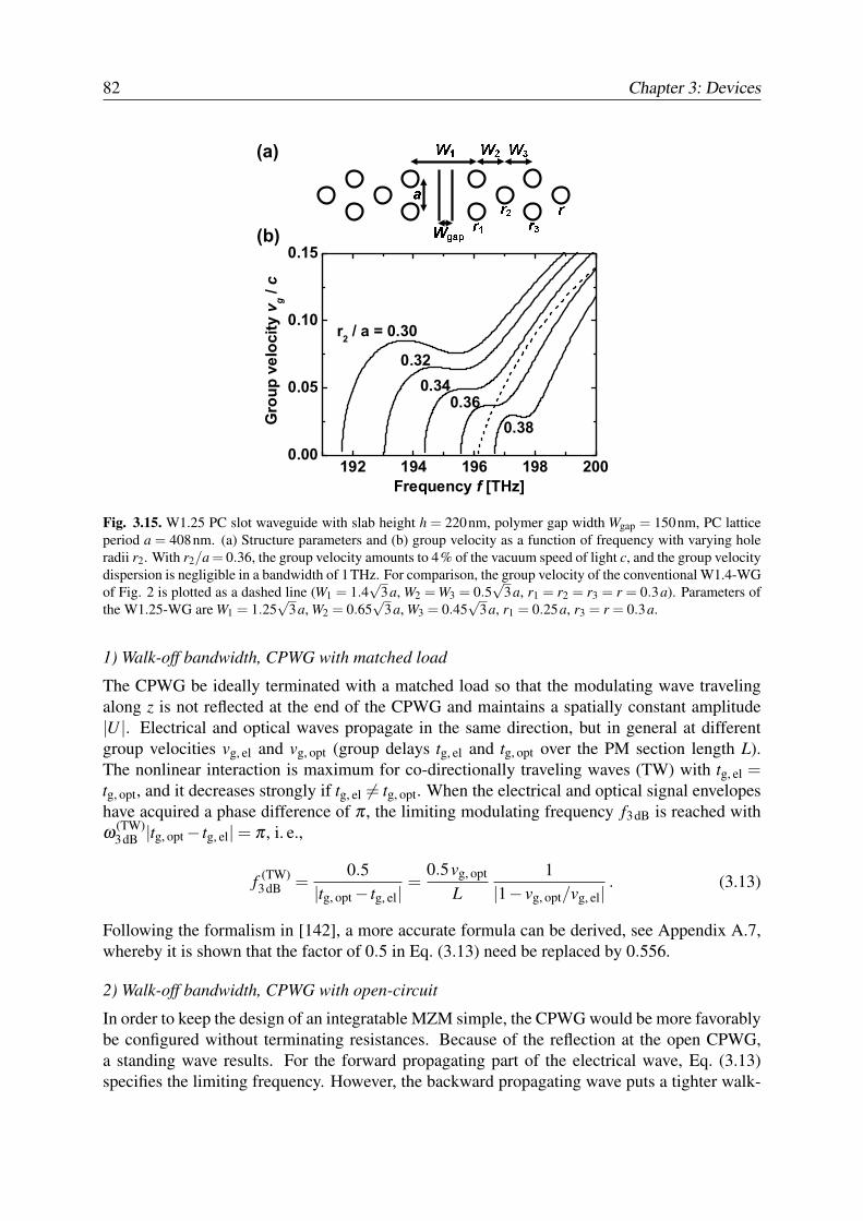
82 Chapter 3: Devices
(a)
(b)
192 194 196 198 2000.00
0.05
0.10
0.15
0.38
0.360.34
0.32
r2 / a = 0.30
Gro
up
ve
locit
y vg / c
Frequency f [THz]
Fig. 3.15. W1.25 PC slot waveguide with slab height h = 220nm, polymer gap width Wgap = 150nm, PC latticeperiod a = 408nm. (a) Structure parameters and (b) group velocity as a function of frequency with varying holeradii r2. With r2/a = 0.36, the group velocity amounts to 4% of the vacuum speed of light c, and the group velocitydispersion is negligible in a bandwidth of 1THz. For comparison, the group velocity of the conventional W1.4-WGof Fig. 2 is plotted as a dashed line (W1 = 1.4
√3a, W2 = W3 = 0.5
√3a, r1 = r2 = r3 = r = 0.3a). Parameters of
the W1.25-WG are W1 = 1.25√
3a, W2 = 0.65√
3a, W3 = 0.45√
3a, r1 = 0.25a, r3 = r = 0.3a.
1) Walk-off bandwidth, CPWG with matched load
The CPWG be ideally terminated with a matched load so that the modulating wave travelingalong z is not reflected at the end of the CPWG and maintains a spatially constant amplitude|U |. Electrical and optical waves propagate in the same direction, but in general at differentgroup velocities vg, el and vg, opt (group delays tg, el and tg, opt over the PM section length L).The nonlinear interaction is maximum for co-directionally traveling waves (TW) with tg, el =tg, opt, and it decreases strongly if tg, el 6= tg, opt. When the electrical and optical signal envelopeshave acquired a phase difference of π , the limiting modulating frequency f3dB is reached withω (TW)
3dB |tg, opt− tg, el|= π , i. e.,
f (TW)3dB =
0.5|tg, opt− tg, el|
=0.5vg, opt
L1
|1− vg, opt/vg, el|. (3.13)
Following the formalism in [142], a more accurate formula can be derived, see Appendix A.7,whereby it is shown that the factor of 0.5 in Eq. (3.13) need be replaced by 0.556.
2) Walk-off bandwidth, CPWG with open-circuit
In order to keep the design of an integratable MZM simple, the CPWG would be more favorablybe configured without terminating resistances. Because of the reflection at the open CPWG,a standing wave results. For the forward propagating part of the electrical wave, Eq. (3.13)specifies the limiting frequency. However, the backward propagating wave puts a tighter walk-
3.3 Compact High-Speed Electro-Optic Modulator 83
off limit, because now the electrical wave has the opposite direction compared to the opticalwave. With similar arguments that led to Eq. (3.13) we find ω3dB|tg, opt + tg, el|= π ,
f3dB =0.5
|tg, opt + tg, el|=
0.5vg, opt
L1
|1+ vg, opt/vg, el|. (3.14)
As above, a more accurate formula can be developed following [142] where the factor of 0.5 inEq. (3.14) is again replaced by 0.556. If vg, opt ¿ vg, el holds, then f3dB ≈ f (TW)
3dB and electricallyshort MZM designs with and without matching load for the CPWG become nearly equivalent,resulting in Eq. (3.12).
π-Voltage Uπ of Phase Modulator
A Mach-Zehnder modulator’s sensitivity is characterized by the π-Voltage Uπ of its phase mod-ulators. For a given PM length L the voltage |U | needed for a π-phase shift is defined to be Uπ .For large modulation sensitivity, Uπ should be small. An optical wave propagating through aPM experiences a nonlinear refractive index change ∆n in proportion to the electric modulatingfield Eel inside the nonlinear PM material,
∆n =−12
r33 n3EO Eel, Eel = U/Wgap . (3.15)
As before, nEO represents the effective linear part of the refractive index in the PM section, andr33 is the (scalar) linear electro-optic coefficient. The total phase shift of the optical wave dueto the index change in a PM section of length L is (following the formalism in Appendix A.7and in [142])
∆Φ =−∆βL =−Γ∆nk0L . (3.16)
The quantity k0 = 2π f0/c is the vacuum wave number. In the process of deriving Eq. (3.16)the so-called field interaction factor Γ was introduced. It quantifies the strength of the nonlinearelectro-optic interaction of modulating field and optical mode in a cross-section A along a latticeperiod a (see Appendix Eqs. (A.76)-(A.80) and [142]),
Γ =∫
gap
nEO
Z0|Ex|2 dV
/∫aℜ(E× H∗) · ez dA ∝
1vg, opt
. (3.17)
In Eq. (3.17), Z0 is the free-space wave impedance, E (x-component Ex) and H are the opticalmodal electric and magnetic fields, and ez is the unit vector in z-direction. The field interactionfactor Γ as defined in Eq. (3.17) is different from the field confinement factor, which is usuallycalculated as a ratio between the optical power in the cross-section of the interaction regionand the total power propagating in the whole modal cross-section. While the field confinementfactor varies between 0 and 1, the field interaction factor Γ can be larger than 1. The integralin the numerator of Eq. (3.17) is a measure of the energy stored in the transverse componentof the propagating optical mode inside the PM along a length a (see Appendix, Eq. (A.18)).The denominator represents the transported power in the modal cross-section. According toEq. (A.19), the energy stored in a volume, when related to the cross-section power of a wavethat crosses this volume, increases in proportion to the reciprocal group velocity of the wave.Because in the numerator of Γ only the dominant transverse field component is regarded, the

84 Chapter 3: Devices
proportionality Γ ∝ 1/vg, opt holds only approximately. Application of a voltage Uπ to the PMresults by definition in a phase change of ∆Φ = π within a length L. From Eq. (3.15)-(3.17),the π-voltage is computed to be
Uπ =c
n3EO f0
Wgap
r33
1LΓ
, Uπ ∝Wgap
r33
1LΓ
∝Wgap
r33
vg, opt
L∝
Wgap
r33f3dB . (3.18)
For the proportionality at the right-hand side of Eq. (3.18), the relations Γ ∝ 1/vg, opt and f3dB ∝vg, opt/L were substituted from Eq. (3.17) and Eq. (3.14).
3.3.5 Optimized Mach-Zehnder ModulatorFor maximizing the modulation bandwidth f3dB, Eq. (3.14), of the MZM amplitude modulatorand for minimizing its π-voltage Uπ , Eq. (3.18), the optical group velocity vg, opt of the PC linedefect WG, its length L, the electro-optic coefficient r33 of the organic material, and the gapwidth Wgap need to be adjusted properly. For an integratable MZM with small length L, thedesign bandwidth f3dB fixes the ratio vg, opt/L. Reducing vg, opt then provides a small lengthL. It also needs to be considered that with lower vg, opt, the disorder-induced losses of the PC-WG increase [58] and the optical bandwidth decreases, so that vg, opt cannot be made arbitrarilysmall.
Structure r2 / a fo (THz) vg,opt/c L ( m) f3dB (GHz)
0.3 196.4 2.4% 4.8 36 103
196.6 3.4% 3.2 54 97
196.9 4.8% 2.2 80 90
196.2 6.4% 1.5 113 83
W1.4
dispersion large
197.7 8.2% 1.1 155 76
0.38 197.5 3.2% 3.1 57 87
0.36 196.5 4.0% 2.2 80 78
0.34 195.8 5.2% 1.6 111 71
0.32 195.2 6.6% 1.1 158 61
W1.25
dispersion
flattened
0.30 194.6 7.9% 0.8 215 53
Table 3.1. Characteristic data for a PC slot waveguide modulator. Group velocity vg,opt, field interaction factor Γ,modulator length L and modulation bandwidth f3dB are estimated at different optical carrier frequencies f0. Weassume an electro-optic coefficient of r33 = 80pm/V. The modulation voltage amplitude for maximum extinctionis fixed to U = Uπ/4 = 1V.
For a small Uπ , the electro-optic organic material is chosen to have a large linear electro-optic coefficient of r33 = 80pm/V [17]. Further, Wgap is chosen as small as compatible withthe fabrication process. A gap width of Wgap = 150nm can be fabricated to good accuracy withadvanced lithographic processes; hence this width is fixed for the present design. Given the gapwidth Wgap, the maximum modulation voltage amplitude is limited in practice by the microwavesource and by dielectric breakdown in the gap.
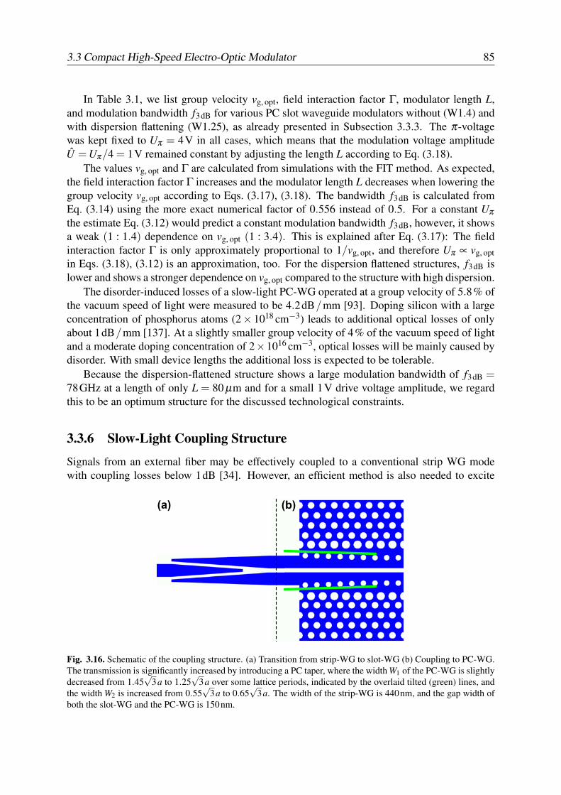
3.3 Compact High-Speed Electro-Optic Modulator 85
In Table 3.1, we list group velocity vg, opt, field interaction factor Γ, modulator length L,and modulation bandwidth f3dB for various PC slot waveguide modulators without (W1.4) andwith dispersion flattening (W1.25), as already presented in Subsection 3.3.3. The π-voltagewas kept fixed to Uπ = 4V in all cases, which means that the modulation voltage amplitudeU = Uπ/4 = 1V remained constant by adjusting the length L according to Eq. (3.18).
The values vg, opt and Γ are calculated from simulations with the FIT method. As expected,the field interaction factor Γ increases and the modulator length L decreases when lowering thegroup velocity vg, opt according to Eqs. (3.17), (3.18). The bandwidth f3dB is calculated fromEq. (3.14) using the more exact numerical factor of 0.556 instead of 0.5. For a constant Uπthe estimate Eq. (3.12) would predict a constant modulation bandwidth f3dB, however, it showsa weak (1 : 1.4) dependence on vg, opt (1 : 3.4). This is explained after Eq. (3.17): The fieldinteraction factor Γ is only approximately proportional to 1/vg, opt, and therefore Uπ ∝ vg, optin Eqs. (3.18), (3.12) is an approximation, too. For the dispersion flattened structures, f3dB islower and shows a stronger dependence on vg, opt compared to the structure with high dispersion.
The disorder-induced losses of a slow-light PC-WG operated at a group velocity of 5.8% ofthe vacuum speed of light were measured to be 4.2dB/mm [93]. Doping silicon with a largeconcentration of phosphorus atoms (2× 1018 cm−3) leads to additional optical losses of onlyabout 1dB/mm [137]. At a slightly smaller group velocity of 4% of the vacuum speed of lightand a moderate doping concentration of 2×1016 cm−3, optical losses will be mainly caused bydisorder. With small device lengths the additional loss is expected to be tolerable.
Because the dispersion-flattened structure shows a large modulation bandwidth of f3dB =78GHz at a length of only L = 80 µm and for a small 1V drive voltage amplitude, we regardthis to be an optimum structure for the discussed technological constraints.
3.3.6 Slow-Light Coupling Structure
Signals from an external fiber may be effectively coupled to a conventional strip WG modewith coupling losses below 1dB [34]. However, an efficient method is also needed to excite
Fig. 3.16. Schematic of the coupling structure. (a) Transition from strip-WG to slot-WG (b) Coupling to PC-WG.The transmission is significantly increased by introducing a PC taper, where the width W1 of the PC-WG is slightlydecreased from 1.45
√3a to 1.25
√3a over some lattice periods, indicated by the overlaid tilted (green) lines, and
the width W2 is increased from 0.55√
3a to 0.65√
3a. The width of the strip-WG is 440nm, and the gap width ofboth the slot-WG and the PC-WG is 150nm.
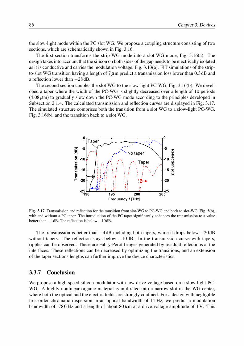
86 Chapter 3: Devices
the slow-light mode within the PC slot WG. We propose a coupling structure consisting of twosections, which are schematically shown in Fig. 3.16.
The first section transforms the strip WG mode into a slot-WG mode, Fig. 3.16(a). Thedesign takes into account that the silicon on both sides of the gap needs to be electrically isolatedas it is conductive and carries the modulation voltage, Fig. 3.13(a). FIT simulations of the strip-to-slot WG transition having a length of 7 µm predict a transmission loss lower than 0.3dB anda reflection lower than −28dB.
The second section couples the slot WG to the slow-light PC-WG, Fig. 3.16(b). We devel-oped a taper where the width of the PC-WG is slightly decreased over a length of 10 periods(4.08 µm) to gradually slow down the PC-WG mode according to the principles developed inSubsection 2.1.4. The calculated transmission and reflection curves are displayed in Fig. 3.17.The simulated structure comprises both the transition from a slot WG to a slow-light PC-WG,Fig. 3.16(b), and the transition back to a slot WG.
190 195 200 205-25
-20
-15
-10
-5
0
-25
-20
-15
-10
-5
0
Tran
smis
sion
[dB
]
Frequency f [THz]
Taper
No taper
Taper
Reflection [dB
]
Fig. 3.17. Transmission and reflection for the transition from slot-WG to PC-WG and back to slot-WG, Fig. 5(b),with and without a PC taper. The introduction of the PC taper significantly enhances the transmission to a valuebetter than −4dB. The reflection is below −10dB.
The transmission is better than −4dB including both tapers, while it drops below −20dBwithout tapers. The reflection stays below −10dB. In the transmission curve with tapers,ripples can be observed. These are Fabry-Perot fringes generated by residual reflections at theinterfaces. These reflections can be decreased by optimizing the transitions, and an extensionof the taper sections lengths can further improve the device characteristics.
3.3.7 Conclusion
We propose a high-speed silicon modulator with low drive voltage based on a slow-light PC-WG. A highly nonlinear organic material is infiltrated into a narrow slot in the WG center,where both the optical and the electric fields are strongly confined. For a design with negligiblefirst-order chromatic dispersion in an optical bandwidth of 1THz, we predict a modulationbandwidth of 78GHz and a length of about 80 µm at a drive voltage amplitude of 1V. This

3.3 Compact High-Speed Electro-Optic Modulator 87
allows transmission at 100Gbit/s. We estimate that the modulation bandwidth is limited by thewalk-off between the optical and electrical signals, while RC−effects do not play a role.

88 Chapter 3: Devices
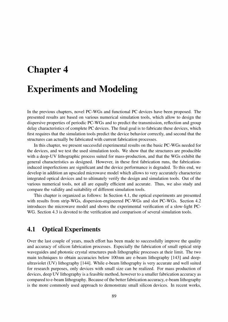
Chapter 4
Experiments and Modeling
In the previous chapters, novel PC-WGs and functional PC devices have been proposed. Thepresented results are based on various numerical simulation tools, which allow to design thedispersive properties of periodic PC-WGs and to predict the transmission, reflection and groupdelay characteristics of complete PC devices. The final goal is to fabricate these devices, whichfirst requires that the simulation tools predict the device behavior correctly, and second that thestructures can actually be fabricated with current fabrication processes.
In this chapter, we present successful experimental results on the basic PC-WGs needed forthe devices, and we test the used simulation tools. We show that the structures are produciblewith a deep-UV lithographic process suited for mass-production, and that the WGs exhibit thegeneral characteristics as designed. However, in these first fabrication runs, the fabrication-induced imperfections are significant and the device performance is degraded. To this end, wedevelop in addition an upscaled microwave model which allows to very accurately characterizeintegrated optical devices and to ultimately verify the design and simulation tools. Out of thevarious numerical tools, not all are equally efficient and accurate. Thus, we also study andcompare the validity and suitability of different simulation tools.
This chapter is organized as follows: In Section 4.1, the optical experiments are presentedwith results from strip-WGs, dispersion-engineered PC-WGs and slot PC-WGs. Section 4.2introduces the microwave model and shows the experimental verification of a slow-light PC-WG. Section 4.3 is devoted to the verification and comparison of several simulation tools.
4.1 Optical Experiments
Over the last couple of years, much effort has been made to successfully improve the qualityand accuracy of silicon fabrication processes. Especially the fabrication of small optical stripwaveguides and photonic crystal structures push lithographic processes at their limit. The twomain techniques to obtain accuracies below 100nm are e-beam lithography [143] and deep-ultraviolet (UV) lithography [144]. While e-beam lithography is very accurate and well suitedfor research purposes, only devices with small size can be realized. For mass production ofdevices, deep UV lithography is a feasible method, however to a smaller fabrication accuracy ascompared to e-beam lithography. Because of the better fabrication accuracy, e-beam lithographyis the more commonly used approach to demonstrate small silicon devices. In recent works,
89
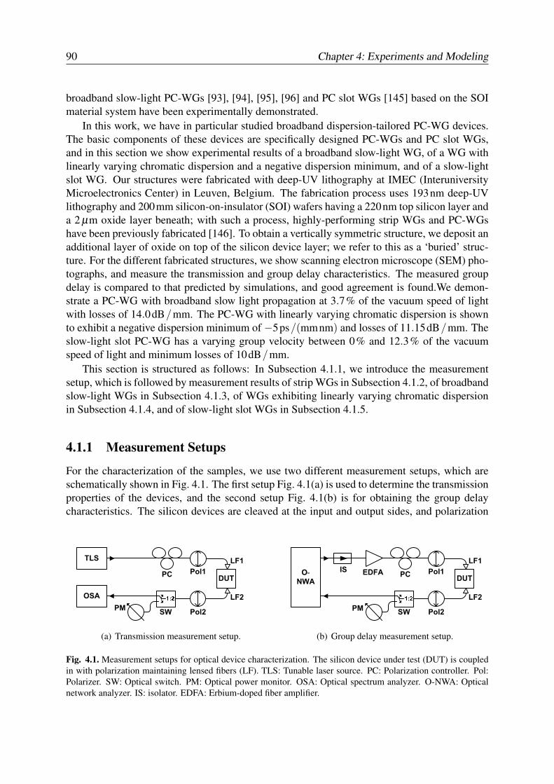
90 Chapter 4: Experiments and Modeling
broadband slow-light PC-WGs [93], [94], [95], [96] and PC slot WGs [145] based on the SOImaterial system have been experimentally demonstrated.
In this work, we have in particular studied broadband dispersion-tailored PC-WG devices.The basic components of these devices are specifically designed PC-WGs and PC slot WGs,and in this section we show experimental results of a broadband slow-light WG, of a WG withlinearly varying chromatic dispersion and a negative dispersion minimum, and of a slow-lightslot WG. Our structures were fabricated with deep-UV lithography at IMEC (InteruniversityMicroelectronics Center) in Leuven, Belgium. The fabrication process uses 193nm deep-UVlithography and 200mm silicon-on-insulator (SOI) wafers having a 220nm top silicon layer anda 2 µm oxide layer beneath; with such a process, highly-performing strip WGs and PC-WGshave been previously fabricated [146]. To obtain a vertically symmetric structure, we deposit anadditional layer of oxide on top of the silicon device layer; we refer to this as a ‘buried’ struc-ture. For the different fabricated structures, we show scanning electron microscope (SEM) pho-tographs, and measure the transmission and group delay characteristics. The measured groupdelay is compared to that predicted by simulations, and good agreement is found.We demon-strate a PC-WG with broadband slow light propagation at 3.7% of the vacuum speed of lightwith losses of 14.0dB/mm. The PC-WG with linearly varying chromatic dispersion is shownto exhibit a negative dispersion minimum of −5ps/(mmnm) and losses of 11.15dB/mm. Theslow-light slot PC-WG has a varying group velocity between 0% and 12.3% of the vacuumspeed of light and minimum losses of 10dB/mm.
This section is structured as follows: In Subsection 4.1.1, we introduce the measurementsetup, which is followed by measurement results of strip WGs in Subsection 4.1.2, of broadbandslow-light WGs in Subsection 4.1.3, of WGs exhibiting linearly varying chromatic dispersionin Subsection 4.1.4, and of slow-light slot WGs in Subsection 4.1.5.
4.1.1 Measurement Setups
For the characterization of the samples, we use two different measurement setups, which areschematically shown in Fig. 4.1. The first setup Fig. 4.1(a) is used to determine the transmissionproperties of the devices, and the second setup Fig. 4.1(b) is for obtaining the group delaycharacteristics. The silicon devices are cleaved at the input and output sides, and polarization
(a) Transmission measurement setup. (b) Group delay measurement setup.
Fig. 4.1. Measurement setups for optical device characterization. The silicon device under test (DUT) is coupledin with polarization maintaining lensed fibers (LF). TLS: Tunable laser source. PC: Polarization controller. Pol:Polarizer. SW: Optical switch. PM: Optical power monitor. OSA: Optical spectrum analyzer. O-NWA: Opticalnetwork analyzer. IS: isolator. EDFA: Erbium-doped fiber amplifier.
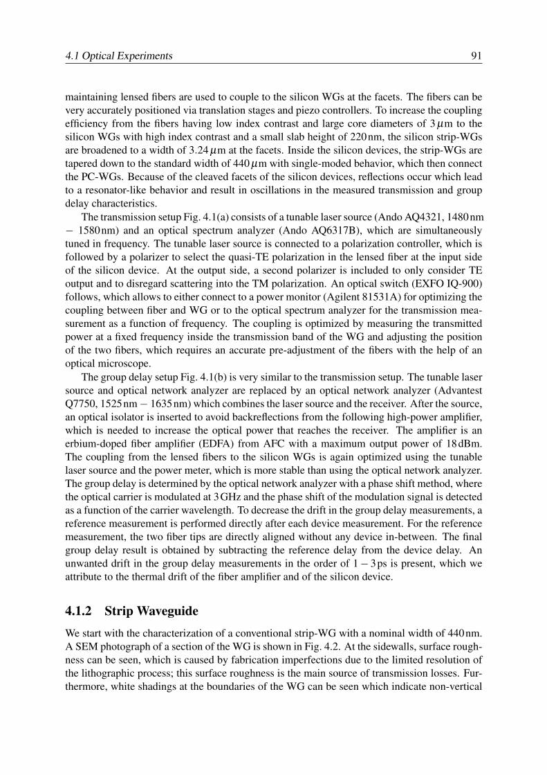
4.1 Optical Experiments 91
maintaining lensed fibers are used to couple to the silicon WGs at the facets. The fibers can bevery accurately positioned via translation stages and piezo controllers. To increase the couplingefficiency from the fibers having low index contrast and large core diameters of 3 µm to thesilicon WGs with high index contrast and a small slab height of 220nm, the silicon strip-WGsare broadened to a width of 3.24 µm at the facets. Inside the silicon devices, the strip-WGs aretapered down to the standard width of 440 µm with single-moded behavior, which then connectthe PC-WGs. Because of the cleaved facets of the silicon devices, reflections occur which leadto a resonator-like behavior and result in oscillations in the measured transmission and groupdelay characteristics.
The transmission setup Fig. 4.1(a) consists of a tunable laser source (Ando AQ4321, 1480nm− 1580nm) and an optical spectrum analyzer (Ando AQ6317B), which are simultaneouslytuned in frequency. The tunable laser source is connected to a polarization controller, which isfollowed by a polarizer to select the quasi-TE polarization in the lensed fiber at the input sideof the silicon device. At the output side, a second polarizer is included to only consider TEoutput and to disregard scattering into the TM polarization. An optical switch (EXFO IQ-900)follows, which allows to either connect to a power monitor (Agilent 81531A) for optimizing thecoupling between fiber and WG or to the optical spectrum analyzer for the transmission mea-surement as a function of frequency. The coupling is optimized by measuring the transmittedpower at a fixed frequency inside the transmission band of the WG and adjusting the positionof the two fibers, which requires an accurate pre-adjustment of the fibers with the help of anoptical microscope.
The group delay setup Fig. 4.1(b) is very similar to the transmission setup. The tunable lasersource and optical network analyzer are replaced by an optical network analyzer (AdvantestQ7750, 1525nm− 1635nm) which combines the laser source and the receiver. After the source,an optical isolator is inserted to avoid backreflections from the following high-power amplifier,which is needed to increase the optical power that reaches the receiver. The amplifier is anerbium-doped fiber amplifier (EDFA) from AFC with a maximum output power of 18dBm.The coupling from the lensed fibers to the silicon WGs is again optimized using the tunablelaser source and the power meter, which is more stable than using the optical network analyzer.The group delay is determined by the optical network analyzer with a phase shift method, wherethe optical carrier is modulated at 3GHz and the phase shift of the modulation signal is detectedas a function of the carrier wavelength. To decrease the drift in the group delay measurements, areference measurement is performed directly after each device measurement. For the referencemeasurement, the two fiber tips are directly aligned without any device in-between. The finalgroup delay result is obtained by subtracting the reference delay from the device delay. Anunwanted drift in the group delay measurements in the order of 1− 3ps is present, which weattribute to the thermal drift of the fiber amplifier and of the silicon device.
4.1.2 Strip Waveguide
We start with the characterization of a conventional strip-WG with a nominal width of 440nm.A SEM photograph of a section of the WG is shown in Fig. 4.2. At the sidewalls, surface rough-ness can be seen, which is caused by fabrication imperfections due to the limited resolution ofthe lithographic process; this surface roughness is the main source of transmission losses. Fur-thermore, white shadings at the boundaries of the WG can be seen which indicate non-vertical
92 Chapter 4: Experiments and Modeling
Fig. 4.2. SEM photograph of strip WG. The sidewalls exhibit roughness due to the limited resolution and accuracyof the lithography. White shadings can be observed at the WG boundaries, which indicate non-vertical sidewalls.
sidewalls. The transmission of a WG with a length of 1,250 µm is shown in Fig. 4.3, whereWG tapers are included in the total length. Strong oscillations caused by reflections at the WGfacets are clearly observed, and for clarity the moving average is added to the graph as reddashed line. The reflections could be removed by adding anti-reflection coatings at the facets,by using angeled facets, or by coupling in light into the silicon WGs with inverted tapers orgrating couplers. The transmission result represents the actually received power by the opticalspectrum analyzer in dBm in a 2nm bandwidth for a laser power of 0dBm. The total transmis-
190 192 194 196 198 200 202-32
-30
-28
-26
-24
Tran
smis
sion
[dB
m]
Frequency f [THz]
Fig. 4.3. Measured transmission of strip-WG. The red dashed line represents the moving average. The WG has anominal width of 440nm and a length of 1,250µm including the WG tapers.
sion loss is the sum of the coupling loss from the fibers to the silicon WG, of the transmissionloss of the WG, and of other additional losses in the setup like the loss of the polarizers, thefibers, the insertion loss of the switch and of the various connectors. By measuring a secondstrip WGs with a smaller device length of 1,000 µm and comparing the transmission, we can es-
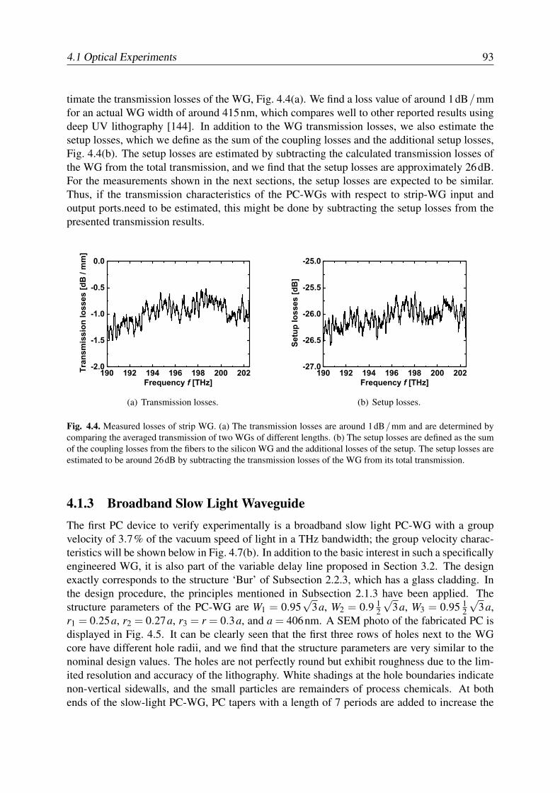
4.1 Optical Experiments 93
timate the transmission losses of the WG, Fig. 4.4(a). We find a loss value of around 1dB/mmfor an actual WG width of around 415nm, which compares well to other reported results usingdeep UV lithography [144]. In addition to the WG transmission losses, we also estimate thesetup losses, which we define as the sum of the coupling losses and the additional setup losses,Fig. 4.4(b). The setup losses are estimated by subtracting the calculated transmission losses ofthe WG from the total transmission, and we find that the setup losses are approximately 26dB.For the measurements shown in the next sections, the setup losses are expected to be similar.Thus, if the transmission characteristics of the PC-WGs with respect to strip-WG input andoutput ports.need to be estimated, this might be done by subtracting the setup losses from thepresented transmission results.
190 192 194 196 198 200 202-2.0
-1.5
-1.0
-0.5
0.0
Tra
nsm
issi
on lo
sses
[dB
/ m
m]
Frequency f [THz]
(a) Transmission losses.
190 192 194 196 198 200 202-27.0
-26.5
-26.0
-25.5
-25.0
Setu
p lo
sses
[dB
]
Frequency f [THz]
(b) Setup losses.
Fig. 4.4. Measured losses of strip WG. (a) The transmission losses are around 1dB/mm and are determined bycomparing the averaged transmission of two WGs of different lengths. (b) The setup losses are defined as the sumof the coupling losses from the fibers to the silicon WG and the additional losses of the setup. The setup losses areestimated to be around 26dB by subtracting the transmission losses of the WG from its total transmission.
4.1.3 Broadband Slow Light WaveguideThe first PC device to verify experimentally is a broadband slow light PC-WG with a groupvelocity of 3.7% of the vacuum speed of light in a THz bandwidth; the group velocity charac-teristics will be shown below in Fig. 4.7(b). In addition to the basic interest in such a specificallyengineered WG, it is also part of the variable delay line proposed in Section 3.2. The designexactly corresponds to the structure ‘Bur’ of Subsection 2.2.3, which has a glass cladding. Inthe design procedure, the principles mentioned in Subsection 2.1.3 have been applied. Thestructure parameters of the PC-WG are W1 = 0.95
√3a, W2 = 0.9 1
2
√3a, W3 = 0.95 1
2
√3a,
r1 = 0.25a, r2 = 0.27a, r3 = r = 0.3a, and a = 406nm. A SEM photo of the fabricated PC isdisplayed in Fig. 4.5. It can be clearly seen that the first three rows of holes next to the WGcore have different hole radii, and we find that the structure parameters are very similar to thenominal design values. The holes are not perfectly round but exhibit roughness due to the lim-ited resolution and accuracy of the lithography. White shadings at the hole boundaries indicatenon-vertical sidewalls, and the small particles are remainders of process chemicals. At bothends of the slow-light PC-WG, PC tapers with a length of 7 periods are added to increase the
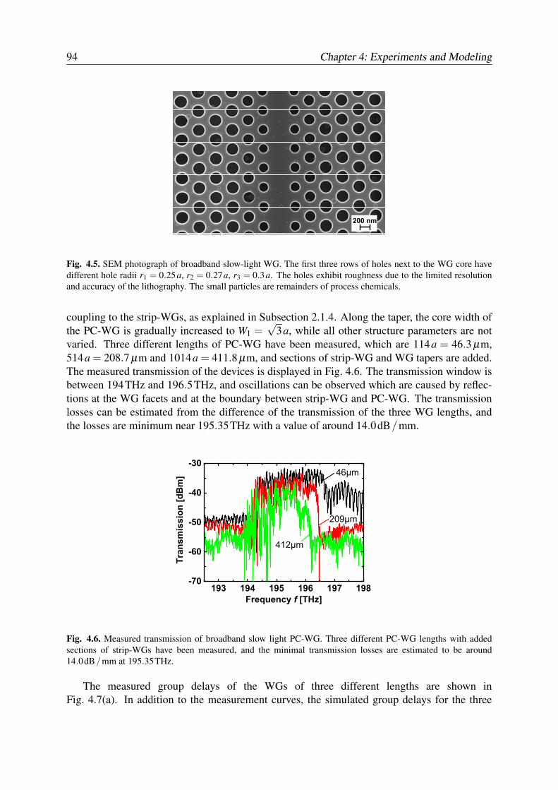
94 Chapter 4: Experiments and Modeling
Fig. 4.5. SEM photograph of broadband slow-light WG. The first three rows of holes next to the WG core havedifferent hole radii r1 = 0.25a, r2 = 0.27a, r3 = 0.3a. The holes exhibit roughness due to the limited resolutionand accuracy of the lithography. The small particles are remainders of process chemicals.
coupling to the strip-WGs, as explained in Subsection 2.1.4. Along the taper, the core width ofthe PC-WG is gradually increased to W1 =
√3a, while all other structure parameters are not
varied. Three different lengths of PC-WG have been measured, which are 114a = 46.3 µm,514a = 208.7 µm and 1014a = 411.8 µm, and sections of strip-WG and WG tapers are added.The measured transmission of the devices is displayed in Fig. 4.6. The transmission window isbetween 194THz and 196.5THz, and oscillations can be observed which are caused by reflec-tions at the WG facets and at the boundary between strip-WG and PC-WG. The transmissionlosses can be estimated from the difference of the transmission of the three WG lengths, andthe losses are minimum near 195.35THz with a value of around 14.0dB/mm.
193 194 195 196 197 198-70
-60
-50
-40
-30
412µm
46µm
209µm
Tran
smis
sion
[dB
m]
Frequency f [THz]
Fig. 4.6. Measured transmission of broadband slow light PC-WG. Three different PC-WG lengths with addedsections of strip-WGs have been measured, and the minimal transmission losses are estimated to be around14.0dB/mm at 195.35THz.
The measured group delays of the WGs of three different lengths are shown inFig. 4.7(a). In addition to the measurement curves, the simulated group delays for the three
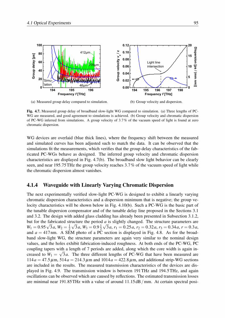
4.1 Optical Experiments 95
194 195 1960
20
40
60
80
100
Simu-lation
Gro
up d
elay
[ps]
Frequency f [THz]
412µm
209µm
46µm
(a) Measured group delay compared to simulation.
194 195 196 197 1980.00
0.02
0.04
0.06
0.08
0.10
0.12
0
5
10
15
20
Gro
up v
eloc
ity v
g / c
Frequency f [THz]
Light lineintersection
Dispersion [ps / (m
m nm
)]
(b) Group velocity and dispersion.
Fig. 4.7. Measured group delay of broadband slow-light WG compared to simulation. (a) Three lengths of PC-WG are measured, and good agreement to simulations is achieved. (b) Group velocity and chromatic dispersionof PC-WG inferred from simulations. A group velocity of 3.7% of the vacuum speed of light is found at zerochromatic dispersion.
WG devices are overlaid (blue thick lines), where the frequency shift between the measuredand simulated curves has been adjusted such to match the data. It can be observed that thesimulations fit the measurements, which verifies that the group delay characteristics of the fab-ricated PC-WGs behave as designed. The inferred group velocity and chromatic dispersioncharacteristics are displayed in Fig. 4.7(b). The broadband slow light behavior can be clearlyseen, and near 195.75THz the group velocity reaches 3.7% of the vacuum speed of light whilethe chromatic dispersion almost vanishes.
4.1.4 Waveguide with Linearly Varying Chromatic Dispersion
The next experimentally verified slow-light PC-WG is designed to exhibit a linearly varyingchromatic dispersion characteristics and a dispersion minimum that is negative; the group ve-locity characteristics will be shown below in Fig. 4.10(b). Such a PC-WG is the basic part ofthe tunable dispersion compensator and of the tunable delay line proposed in the Sections 3.1and 3.2. The design with added glass cladding has already been presented in Subsection 3.1.2,but for the fabricated structure the period a is slightly changed. The structure parameters areW1 = 0.95
√3a, W2 = 1
2
√3a, W3 = 0.9 1
2
√3a, r1 = 0.25a, r2 = 0.32a, r3 = 0.34a, r = 0.3a,
and a = 417nm. A SEM photo of a PC section is displayed in Fig. 4.8. As for the broad-band slow-light WG, the structure parameters are again very similar to the nominal designvalues, and the holes exhibit fabrication-induced roughness. At both ends of the PC-WG, PCcoupling tapers with a length of 7 periods are added, along which the core width is again in-creased to W1 =
√3a. The three different lengths of PC-WG that have been measured are
114a = 47.5 µm, 514a = 214.3 µm and 1014a = 422.8 µm, and additional strip-WG sectionsare included in the results. The measured transmission characteristics of the devices are dis-played in Fig. 4.9. The transmission window is between 191THz and 194.5THz, and againoscillations can be observed which are caused by reflections. The estimated transmission lossesare minimal near 191.85THz with a value of around 11.15dB/mm. At certain spectral posi-
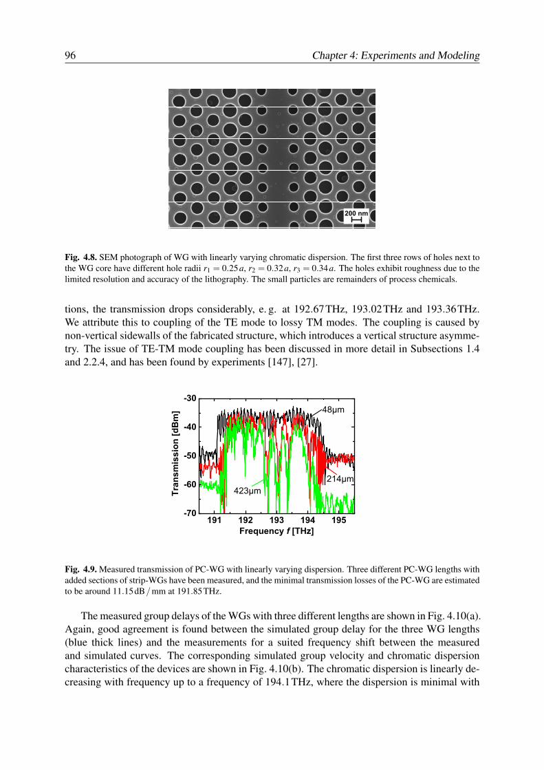
96 Chapter 4: Experiments and Modeling
Fig. 4.8. SEM photograph of WG with linearly varying chromatic dispersion. The first three rows of holes next tothe WG core have different hole radii r1 = 0.25a, r2 = 0.32a, r3 = 0.34a. The holes exhibit roughness due to thelimited resolution and accuracy of the lithography. The small particles are remainders of process chemicals.
tions, the transmission drops considerably, e. g. at 192.67THz, 193.02THz and 193.36THz.We attribute this to coupling of the TE mode to lossy TM modes. The coupling is caused bynon-vertical sidewalls of the fabricated structure, which introduces a vertical structure asymme-try. The issue of TE-TM mode coupling has been discussed in more detail in Subsections 1.4and 2.2.4, and has been found by experiments [147], [27].
191 192 193 194 195-70
-60
-50
-40
-30
Tran
smis
sion
[dB
m]
Frequency f [THz]
423µm214µm
48µm
Fig. 4.9. Measured transmission of PC-WG with linearly varying dispersion. Three different PC-WG lengths withadded sections of strip-WGs have been measured, and the minimal transmission losses of the PC-WG are estimatedto be around 11.15dB/mm at 191.85THz.
The measured group delays of the WGs with three different lengths are shown in Fig. 4.10(a).Again, good agreement is found between the simulated group delay for the three WG lengths(blue thick lines) and the measurements for a suited frequency shift between the measuredand simulated curves. The corresponding simulated group velocity and chromatic dispersioncharacteristics of the devices are shown in Fig. 4.10(b). The chromatic dispersion is linearly de-creasing with frequency up to a frequency of 194.1THz, where the dispersion is minimal with
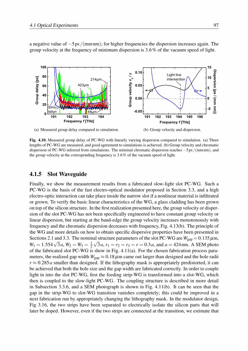
4.1 Optical Experiments 97
a negative value of −5ps/(mmnm); for higher frequencies the dispersion increases again. Thegroup velocity at the frequency of minimum dispersion is 3.6% of the vacuum speed of light.
191 192 193 1940
20
40
60
80
100
Gro
up d
elay
[ps]
Frequency f [THz]
423µm214µm
48µmSimu-lation
(a) Measured group delay compared to simulation.
-0.05
0.00
0.05
0.10
-5
0
5
10
15
191 192 193 194 195 196
Gro
up v
eloc
ity v
g / c Light line
intersection
Dispersion [ps / (m
m nm
)]
Frequency f [THz]
(b) Group velocity and dispersion.
Fig. 4.10. Measured group delay of PC-WG with linearly varying dispersion compared to simulation. (a) Threelengths of PC-WG are measured, and good agreement to simulations is achieved. (b) Group velocity and chromaticdispersion of PC-WG inferred from simulations. The minimal chromatic dispersion reaches −5ps/(mmnm), andthe group velocity at the corresponding frequency is 3.6% of the vacuum speed of light.
4.1.5 Slot WaveguideFinally, we show the measurement results from a fabricated slow-light slot PC-WG. Such aPC-WG is the basis of the fast electro-optical modulator proposed in Section 3.3, and a highelectro-optic interaction can take place inside the narrow slot if a nonlinear material is infiltratedor grown. To verify the basic linear characteristics of the WG, a glass cladding has been grownon top of the silicon structure. In the first realization presented here, the group velocity or disper-sion of the slot PC-WG has not been specifically engineered to have constant group velocity orlinear dispersion, but starting at the band-edge the group velocity increases monotonously withfrequency and the chromatic dispersion decreases with frequency, Fig. 4.13(b). The principle ofthe WG and more details on how to obtain specific dispersive properties have been presented inSections 2.1 and 3.3. The nominal structure parameters of the slot PC-WG are Wgap = 0.135 µm,W1 = 1.554
√3a, W2 = W3 = 1
2
√3a, r1 = r2 = r3 = r = 0.3a, and a = 424nm. A SEM photo
of the fabricated slot PC-WG is show in Fig. 4.11(a). For the chosen fabrication process para-meters, the realized gap width Wgap ≈ 0.18 µm came out larger than designed and the hole radiir ≈ 0.285a smaller than designed. If the lithography mask is appropriately predistorted, it canbe achieved that both the hole size and the gap width are fabricated correctly. In order to couplelight in into the slot PC-WG, first the feeding strip-WG is transformed into a slot-WG, whichthen is coupled to the slow-light PC-WG. The coupling structure is described in more detailin Subsection 3.3.6, and a SEM photograph is shown in Fig. 4.11(b). It can be seen that thegap in the strip-WG to slot-WG transition vanishes completely; this could be improved in anext fabrication run by appropriately changing the lithography mask. In the modulator design,Fig 3.16, the two strips have been separated to electrically isolate the silicon parts that willlater be doped. However, even if the two strips are connected at the transition, we estimate that
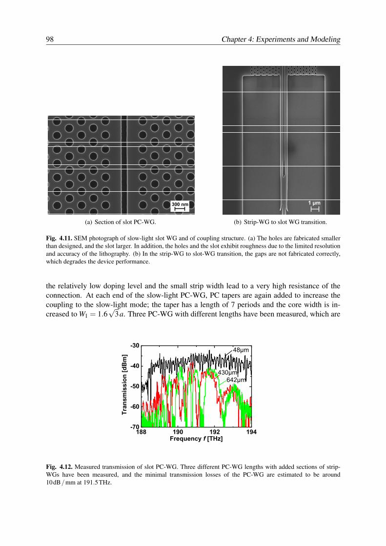
98 Chapter 4: Experiments and Modeling
(a) Section of slot PC-WG.
1 µm
(b) Strip-WG to slot WG transition.
Fig. 4.11. SEM photograph of slow-light slot WG and of coupling structure. (a) The holes are fabricated smallerthan designed, and the slot larger. In addition, the holes and the slot exhibit roughness due to the limited resolutionand accuracy of the lithography. (b) In the strip-WG to slot-WG transition, the gaps are not fabricated correctly,which degrades the device performance.
the relatively low doping level and the small strip width lead to a very high resistance of theconnection. At each end of the slow-light PC-WG, PC tapers are again added to increase thecoupling to the slow-light mode; the taper has a length of 7 periods and the core width is in-creased to W1 = 1.6
√3a. Three PC-WG with different lengths have been measured, which are
188 190 192 194-70
-60
-50
-40
-3048µm
430µm642µm
Tran
smis
sion
[dB
m]
Frequency f [THz]
Fig. 4.12. Measured transmission of slot PC-WG. Three different PC-WG lengths with added sections of strip-WGs have been measured, and the minimal transmission losses of the PC-WG are estimated to be around10dB/mm at 191.5THz.
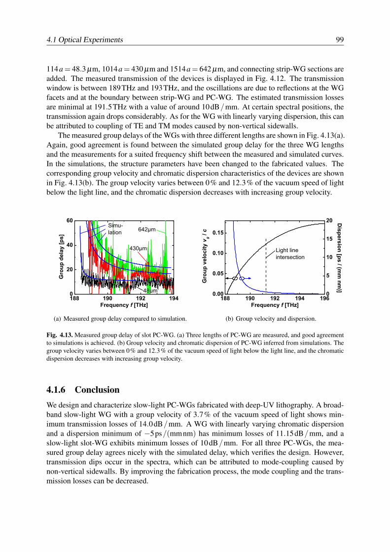
4.1 Optical Experiments 99
114a = 48.3 µm, 1014a = 430 µm and 1514a = 642 µm, and connecting strip-WG sections areadded. The measured transmission of the devices is displayed in Fig. 4.12. The transmissionwindow is between 189THz and 193THz, and the oscillations are due to reflections at the WGfacets and at the boundary between strip-WG and PC-WG. The estimated transmission lossesare minimal at 191.5THz with a value of around 10dB/mm. At certain spectral positions, thetransmission again drops considerably. As for the WG with linearly varying dispersion, this canbe attributed to coupling of TE and TM modes caused by non-vertical sidewalls.
The measured group delays of the WGs with three different lengths are shown in Fig. 4.13(a).Again, good agreement is found between the simulated group delay for the three WG lengthsand the measurements for a suited frequency shift between the measured and simulated curves.In the simulations, the structure parameters have been changed to the fabricated values. Thecorresponding group velocity and chromatic dispersion characteristics of the devices are shownin Fig. 4.13(b). The group velocity varies between 0% and 12.3% of the vacuum speed of lightbelow the light line, and the chromatic dispersion decreases with increasing group velocity.
188 190 192 1940
20
40
60
48µm
430µm
642µmSimu-lation
Gro
up d
elay
[ps]
Frequency f [THz]
(a) Measured group delay compared to simulation.
188 190 192 194 1960.00
0.05
0.10
0.15
0
5
10
15
20
Gro
up v
eloc
ity v
g / c
Frequency f [THz]
Light lineintersection
Dispersion [ps / (m
m nm
)]
(b) Group velocity and dispersion.
Fig. 4.13. Measured group delay of slot PC-WG. (a) Three lengths of PC-WG are measured, and good agreementto simulations is achieved. (b) Group velocity and chromatic dispersion of PC-WG inferred from simulations. Thegroup velocity varies between 0% and 12.3% of the vacuum speed of light below the light line, and the chromaticdispersion decreases with increasing group velocity.
4.1.6 ConclusionWe design and characterize slow-light PC-WGs fabricated with deep-UV lithography. A broad-band slow-light WG with a group velocity of 3.7% of the vacuum speed of light shows min-imum transmission losses of 14.0dB/mm. A WG with linearly varying chromatic dispersionand a dispersion minimum of −5ps/(mmnm) has minimum losses of 11.15dB/mm, and aslow-light slot-WG exhibits minimum losses of 10dB/mm. For all three PC-WGs, the mea-sured group delay agrees nicely with the simulated delay, which verifies the design. However,transmission dips occur in the spectra, which can be attributed to mode-coupling caused bynon-vertical sidewalls. By improving the fabrication process, the mode coupling and the trans-mission losses can be decreased.

100 Chapter 4: Experiments and Modeling
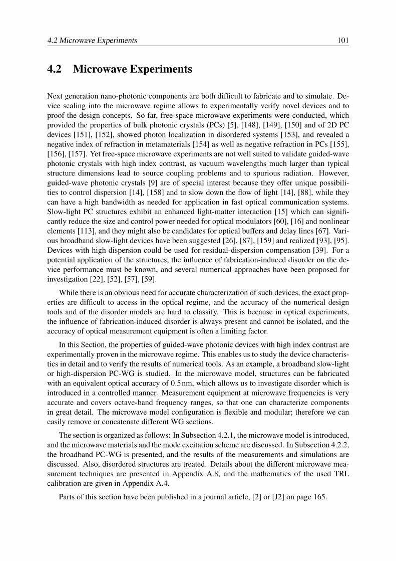
4.2 Microwave Experiments 101
4.2 Microwave Experiments
Next generation nano-photonic components are both difficult to fabricate and to simulate. De-vice scaling into the microwave regime allows to experimentally verify novel devices and toproof the design concepts. So far, free-space microwave experiments were conducted, whichprovided the properties of bulk photonic crystals (PCs) [5], [148], [149], [150] and of 2D PCdevices [151], [152], showed photon localization in disordered systems [153], and revealed anegative index of refraction in metamaterials [154] as well as negative refraction in PCs [155],[156], [157]. Yet free-space microwave experiments are not well suited to validate guided-wavephotonic crystals with high index contrast, as vacuum wavelengths much larger than typicalstructure dimensions lead to source coupling problems and to spurious radiation. However,guided-wave photonic crystals [9] are of special interest because they offer unique possibili-ties to control dispersion [14], [158] and to slow down the flow of light [14], [88], while theycan have a high bandwidth as needed for application in fast optical communication systems.Slow-light PC structures exhibit an enhanced light-matter interaction [15] which can signifi-cantly reduce the size and control power needed for optical modulators [60], [16] and nonlinearelements [113], and they might also be candidates for optical buffers and delay lines [67]. Vari-ous broadband slow-light devices have been suggested [26], [87], [159] and realized [93], [95].Devices with high dispersion could be used for residual-dispersion compensation [39]. For apotential application of the structures, the influence of fabrication-induced disorder on the de-vice performance must be known, and several numerical approaches have been proposed forinvestigation [22], [52], [57], [59].
While there is an obvious need for accurate characterization of such devices, the exact prop-erties are difficult to access in the optical regime, and the accuracy of the numerical designtools and of the disorder models are hard to classify. This is because in optical experiments,the influence of fabrication-induced disorder is always present and cannot be isolated, and theaccuracy of optical measurement equipment is often a limiting factor.
In this Section, the properties of guided-wave photonic devices with high index contrast areexperimentally proven in the microwave regime. This enables us to study the device characteris-tics in detail and to verify the results of numerical tools. As an example, a broadband slow-lightor high-dispersion PC-WG is studied. In the microwave model, structures can be fabricatedwith an equivalent optical accuracy of 0.5nm, which allows us to investigate disorder which isintroduced in a controlled manner. Measurement equipment at microwave frequencies is veryaccurate and covers octave-band frequency ranges, so that one can characterize componentsin great detail. The microwave model configuration is flexible and modular; therefore we caneasily remove or concatenate different WG sections.
The section is organized as follows: In Subsection 4.2.1, the microwave model is introduced,and the microwave materials and the mode excitation scheme are discussed. In Subsection 4.2.2,the broadband PC-WG is presented, and the results of the measurements and simulations arediscussed. Also, disordered structures are treated. Details about the different microwave mea-surement techniques are presented in Appendix A.8, and the mathematics of the used TRLcalibration are given in Appendix A.4.
Parts of this section have been published in a journal article, [2] or [J2] on page 165.
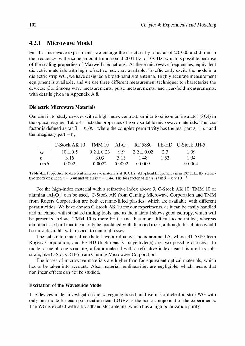
102 Chapter 4: Experiments and Modeling
4.2.1 Microwave ModelFor the microwave experiments, we enlarge the structure by a factor of 20,000 and diminishthe frequency by the same amount from around 200THz to 10GHz, which is possible becauseof the scaling properties of Maxwell’s equations. At these microwave frequencies, equivalentdielectric materials with high refractive index are available. To efficiently excite the mode in adielectric strip WG, we have designed a broad-band slot antenna. Highly accurate measurementequipment is available, and we use three different measurement techniques to characterize thedevices: Continuous wave measurements, pulse measurements, and near-field measurements,with details given in Appendix A.8.
Dielectric Microwave Materials
Our aim is to study devices with a high-index contrast, similar to silicon on insulator (SOI) inthe optical regime. Table 4.1 lists the properties of some suitable microwave materials. The lossfactor is defined as tanδ = εr/εri, where the complex permittivity has the real part εr = n2 andthe imaginary part −εri.
C-Stock AK 10 TMM 10 Al2O3 RT 5880 PE-HD C-Stock RH-5εr 10±0.5 9.2±0.23 9.9 2.2±0.02 2.3 1.09n 3.16 3.03 3.15 1.48 1.52 1.04tanδ 0.002 0.0022 0.0002 0.0009 0.0004
Table 4.1. Properties fo different microwave materials at 10GHz. At optical frequencies near 193THz, the refrac-tive index of silicon n = 3.48 and of glass n = 1.44. The loss factor of glass is tanδ = 6×10⁻¹².
For the high-index material with a refractive index above 3, C-Stock AK 10, TMM 10 oralumina (Al2O3) can be used. C-Stock AK from Cuming Microwave Corporation and TMMfrom Rogers Corporation are both ceramic-filled plastics, which are available with differentpermittivities. We have chosen C-Stock AK 10 for our experiments, as it can be easily handledand machined with standard milling tools, and as the material shows good isotropy, which willbe presented below. TMM 10 is more brittle and thus more difficult to be milled, whereasalumina is so hard that it can only be machined with diamond tools, although this choice wouldbe most desirable with respect to material losses.
The substrate material needs to have a refractive index around 1.5, where RT 5880 fromRogers Corporation, and PE-HD (high-density polyethylene) are two possible choices. Tomodel a membrane structure, a foam material with a refractive index near 1 is used as sub-strate, like C-Stock RH-5 from Cuming Microwave Corporation.
The losses of microwave materials are higher than for equivalent optical materials, whichhas to be taken into account. Also, material nonlinearities are negligible, which means thatnonlinear effects can not be studied.
Excitation of the Waveguide Mode
The devices under investigation are waveguide-based, and we use a dielectric strip-WG withonly one mode for each polarization near 10GHz as the basic component of the experiments.The WG is excited with a broadband slot antenna, which has a high polarization purity.
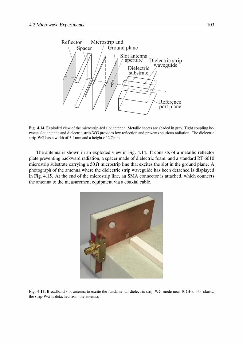
4.2 Microwave Experiments 103
ReflectorSpacer
Microstrip and
Slot antennaaperture Dielectric strip
waveguideDielectricsubstrate
Referenceport plane
Ground plane
Fig. 4.14. Exploded view of the microstrip-fed slot antenna. Metallic sheets are shaded in gray. Tight coupling be-tween slot antenna and dielectric strip-WG provides low reflection and prevents spurious radiation. The dielectricstrip-WG has a width of 5.4mm and a height of 2.7mm.
The antenna is shown in an exploded view in Fig. 4.14. It consists of a metallic reflectorplate preventing backward radiation, a spacer made of dielectric foam, and a standard RT 6010microstrip substrate carrying a 50Ω microstrip line that excites the slot in the ground plane. Aphotograph of the antenna where the dielectric strip waveguide has been detached is displayedin Fig. 4.15. At the end of the microstrip line, an SMA connector is attached, which connectsthe antenna to the measurement equipment via a coaxial cable.
Fig. 4.15. Broadband slot antenna to excite the fundamental dielectric strip-WG mode near 10GHz. For clarity,the strip-WG is detached from the antenna.
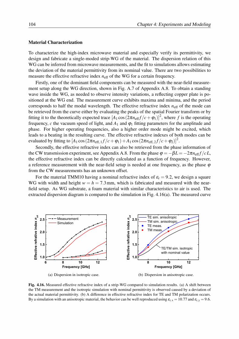
104 Chapter 4: Experiments and Modeling
Material Characterization
To characterize the high-index microwave material and especially verify its permittivity, wedesign and fabricate a single-moded strip-WG of the material. The dispersion relation of thisWG can be inferred from microwave measurements, and the fit to simulations allows estimatingthe deviation of the material permittivity from its nominal value. There are two possibilities tomeasure the effective refractive index neff of the WG for a certain frequency.
Firstly, one of the dominant field components can be measured with the near-field measure-ment setup along the WG direction, shown in Fig. A.7 of Appendix A.8. To obtain a standingwave inside the WG, as needed to observe intensity variations, a reflecting copper plate is po-sitioned at the WG end. The measurement curve exhibits maxima and minima, and the periodcorresponds to half the modal wavelength. The effective refractive index neff of the mode canbe retrieved from the curve either by evaluating the peaks of the spatial Fourier transform or byfitting it to the theoretically expected trace [A1 cos(2πneff f /c+ϕ1)]
2, where f is the operatingfrequency, c the vacuum speed of light, and A1 and ϕ1 fitting parameters for the amplitude andphase. For higher operating frequencies, also a higher order mode might be excited, whichleads to a beating in the resulting curve. The effective refractive indexes of both modes can beevaluated by fitting to [A1 cos(2πneff, 1 f/c+ϕ1)+A1 cos(2πneff, 2 f/c+ϕ2)]
2.Secondly, the effective refractive index can also be retrieved from the phase information of
the CW transmission experiment, see Appendix A.8. From the phase ϕ =−βL =−2πneff f /cL,the effective refractive index can be directly calculated as a function of frequency. However,a reference measurement with the near-field setup is needed at one frequency, as the phase ϕfrom the CW measurements has an unknown offset.
For the material TMM10 having a nominal refractive index of εr = 9.2, we design a squareWG with width and height w = h = 7.3mm, which is fabricated and measured with the near-field setup. As WG substrate, a foam material with similar characteristics to air is used. Theextracted dispersion diagram is compared to the simulation in Fig. 4.16(a). The measured curve
6 8 10 121.0
1.5
2.0
2.5 Measurement Simulation
Effe
ctiv
e re
frat
ive
inde
x n ef
f
Frequency [GHz]
(a) Dispersion in isotropic case.
8 10 121.0
1.5
2.0
2.5 TE sim. anisotropic TM sim. anisotropic TE meas. TM meas.
Effe
ctiv
e re
frat
ive
inde
x n ef
f
Frequency [GHz]
TE/TM sim. isotropicwith nominal value
(b) Dispersion in anisotropic case.
Fig. 4.16. Measured effective refractive index of a strip-WG compared to simulation results. (a) A shift betweenthe TM measurement and the isotropic simulation with nominal permittivity is observed caused by a deviation ofthe actual material permittivity. (b) A difference in effective refractive index for TE and TM polarization occurs.By a simulation with an anisotropic material, the behavior can be well reproduced using εr, x = 10.77 and εr, y = 9.6.
4.2 Microwave Experiments 105
is shifted in frequency of about 0.5GHz with respect to the simulated curve, which indicates adeviation in the material permittivity of TMM10 from its nominal value. As the WG is of squareshape, the TE and TM modes should theoretically have exactly the same dispersion relation.However, we find that a significant difference occurs between the TE and TM mode dispersion,as shown in Fig. 4.16(b). This difference can only be explained by a material anisotropy, whichmeans that there are different permittivity values for the two orthogonal transverse electric fielddirections x and y. By modeling a WG with an anisotropic material also in the simulations, themeasurement results can be better reproduced, and with εr, x = 10.77 and εr, y = 9.6 we find agood match.
We also fabricate and measure strip-WGs with the material CAK-10, and the measurementsshow a negligible anisotropy, but also significant deviations from the nominal permittivity. Fordifferent material lots, we infer relative permittivities εr between 8.9 and 10.1. The isotropyof CAK-10 is another advantage of the material in addition to the good machinability, and thematerial is used for the following experiments. A single-moded WG is designed with a widthw = 8.1mm and a height h = 5.4mm.
4.2.2 Broadband Slow Light Waveguide
Numerous optical components can be studied with the microwave model, like waveguide cou-plers, ring resonators and photonic crystals. We characterize a slow-light or high-dispersionphotonic crystal waveguide in detail, which exhibits a group velocity of 4% of the vacuumspeed of light over a bandwidth of more than 1THz, and a region with a chromatic dispersionof 4ps/(mmnm) over 1THz. The results of the CW, pulse transmission and near field mea-surements are presented, and used to verify the accuracy of the FIT simulation method. Also,the delay-bandwidth product of the WG is estimated. For a real device, fabrication-induced dis-order is unavoidable, and we show experimental results of the influence of 5% radial disorder.
Structure and Design
Following a recent proposal [26] we designed the single-moded broadband slow-light PC-WGas an air-bridge structure for a slab permittivity of εr = 10. A triangular lattice PC was chosenhaving a slab thickness h/a = 0.6, hole radii r/a = 0.25, and a reduced width W0.75 PC-WG.The period of the PC is a = 0.45 µm in the optical regime and a = 9mm for the microwavemodel. Fig. 4.17 shows the band diagram of the structure, generated with the FIT eigenmodesolver. The region with low group velocity is indicated in the figure as “Slow light region”;it is centered around a frequency of 205THz. To efficiently couple the PC-WG to a feedingstrip-WG, a PC taper is introduced, where the width of the PC-WG is adiabatically increasedfrom W0.75 to W0.8 over a length of 5 periods [26]. The structure is schematically shown inFig. 4.18(a). The field distribution of the slow-light mode has considerable field values in theregion of the air holes. Along the taper this field is transformed to be confined mainly to thewaveguide core for a better match to the field distribution of the strip WG. Simulations withthe FIT transient solver indicate a coupling loss below 1.25dB per interface and a reflectionbelow 10dB in the slow-light regime, which are much better values than for direct coupling tothe strip-WG without taper [100]. We fabricated a microwave model as shown in Fig. 4.18 withcoupling tapers and 30 periods of the W0.75 PC-WG.
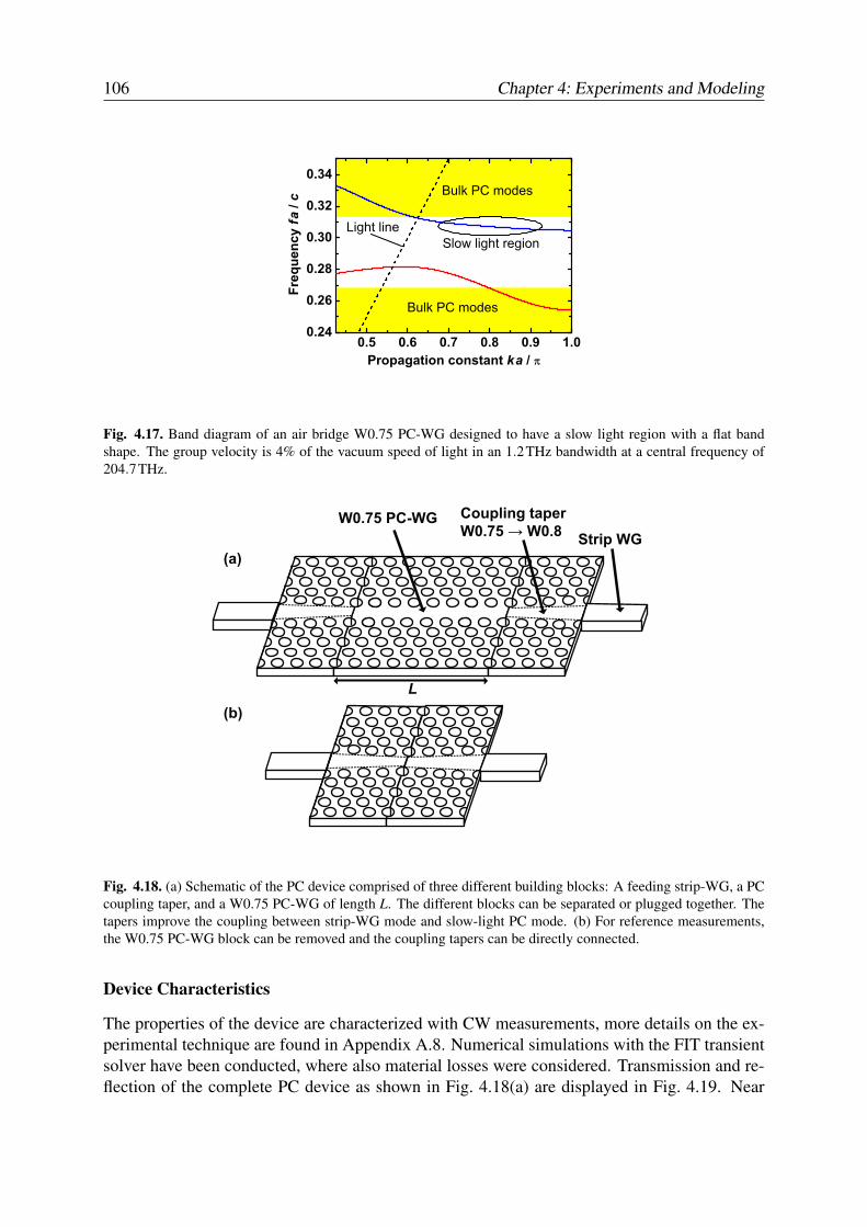
106 Chapter 4: Experiments and Modeling
0.5 0.6 0.7 0.8 0.9 1.00.24
0.26
0.28
0.30
0.32
0.34Bulk PC modes
Bulk PC modes
Slow light region
Freq
uenc
y f a
/ c
Propagation constant k a /
Light line
Fig. 4.17. Band diagram of an air bridge W0.75 PC-WG designed to have a slow light region with a flat bandshape. The group velocity is 4% of the vacuum speed of light in an 1.2THz bandwidth at a central frequency of204.7THz.
Fig. 4.18. (a) Schematic of the PC device comprised of three different building blocks: A feeding strip-WG, a PCcoupling taper, and a W0.75 PC-WG of length L. The different blocks can be separated or plugged together. Thetapers improve the coupling between strip-WG mode and slow-light PC mode. (b) For reference measurements,the W0.75 PC-WG block can be removed and the coupling tapers can be directly connected.
Device Characteristics
The properties of the device are characterized with CW measurements, more details on the ex-perimental technique are found in Appendix A.8. Numerical simulations with the FIT transientsolver have been conducted, where also material losses were considered. Transmission and re-flection of the complete PC device as shown in Fig. 4.18(a) are displayed in Fig. 4.19. Near
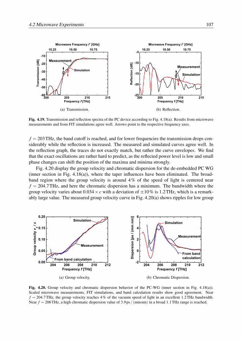
4.2 Microwave Experiments 107
200 205 210 215-60
-50
-40
-30
-20
-10
10.25 10.50 10.75
Measurement
Tran
smis
sion
[dB
]
Frequency f [THz]
Simulation
Microwave Frequency f´ [GHz]
(a) Transmission.
200 205 210 215-25
-20
-15
-10
-510.25 10.50 10.75
Ref
lect
ion
[dB
]
Frequency f [THz]
Simulation
Measurement
Microwave Frequency f´ [GHz]
(b) Reflection.
Fig. 4.19. Transmission and reflection spectra of the PC device according to Fig. 4.18(a). Results from microwavemeasurements and from FIT simulations agree well. Arrows point to the respective frequency axes.
f = 203THz, the band cutoff is reached, and for lower frequencies the transmission drops con-siderably while the reflection is increased. The measured and simulated curves agree well. Inthe reflection graph, the traces do not exactly match, but rather the curve envelopes. We findthat the exact oscillations are rather hard to predict, as the reflected power level is low and smallphase changes can shift the position of the maxima and minima strongly.
Fig. 4.20 display the group velocity and chromatic dispersion for the de-embedded PC WG(inner section in Fig. 4.18(a)), where the taper influences have been eliminated. The broad-band region where the group velocity is around 4% of the speed of light is centered nearf = 204.7THz, and here the chromatic dispersion has a minimum. The bandwidth where thegroup velocity varies about 0.034× c with a deviation of ±10% is 1.2THz, which is a remark-ably large value. The measured group velocity curve in Fig. 4.20(a) shows ripples for low group
204 206 208 210 2120.00
0.05
0.10
0.15
0.20
Measurement
Gro
up v
eloc
ity v
g / c
Frequency f [THz]
Simulation
From band calculation
(a) Group velocity.
204 206 208 210 212-2
0
2
4
6
Simulation
Measurement
From band calculation
Dis
pers
ion
[ps
/ (m
m n
m)]
Frequency f [THz]
(b) Chromatic Dispersion.
Fig. 4.20. Group velocity and chromatic dispersion behavior of the PC-WG (inner section in Fig. 4.18(a)).Scaled microwave measurements, FIT simulations, and band calculation results show good agreement. Nearf = 204.7THz, the group velocity reaches 4% of the vacuum speed of light in an excellent 1.2THz bandwidth.Near f = 206THz, a high chromatic dispersion value of 3.9ps/(mmnm) in a broad 1.1THz range is reached.
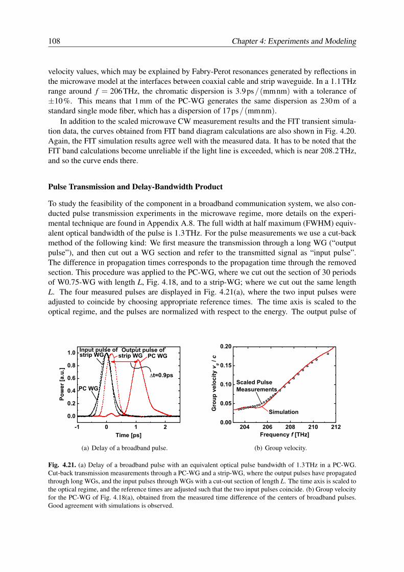
108 Chapter 4: Experiments and Modeling
velocity values, which may be explained by Fabry-Perot resonances generated by reflections inthe microwave model at the interfaces between coaxial cable and strip waveguide. In a 1.1THzrange around f = 206THz, the chromatic dispersion is 3.9ps/(mmnm) with a tolerance of±10%. This means that 1mm of the PC-WG generates the same dispersion as 230m of astandard single mode fiber, which has a dispersion of 17ps/(mmnm).
In addition to the scaled microwave CW measurement results and the FIT transient simula-tion data, the curves obtained from FIT band diagram calculations are also shown in Fig. 4.20.Again, the FIT simulation results agree well with the measured data. It has to be noted that theFIT band calculations become unreliable if the light line is exceeded, which is near 208.2THz,and so the curve ends there.
Pulse Transmission and Delay-Bandwidth Product
To study the feasibility of the component in a broadband communication system, we also con-ducted pulse transmission experiments in the microwave regime, more details on the experi-mental technique are found in Appendix A.8. The full width at half maximum (FWHM) equiv-alent optical bandwidth of the pulse is 1.3THz. For the pulse measurements we use a cut-backmethod of the following kind: We first measure the transmission through a long WG (“outputpulse”), and then cut out a WG section and refer to the transmitted signal as “input pulse”.The difference in propagation times corresponds to the propagation time through the removedsection. This procedure was applied to the PC-WG, where we cut out the section of 30 periodsof W0.75-WG with length L, Fig. 4.18, and to a strip-WG; where we cut out the same lengthL. The four measured pulses are displayed in Fig. 4.21(a), where the two input pulses wereadjusted to coincide by choosing appropriate reference times. The time axis is scaled to theoptical regime, and the pulses are normalized with respect to the energy. The output pulse of
-1 0 1 2
0.0
0.2
0.4
0.6
0.8
1.0 strip WG
PC WG
strip WG
Pow
er [a
.u.]
Time [ps]
Input pulse ofPC WG
t=0.9ps
Output pulse of
(a) Delay of a broadband pulse.
204 206 208 210 2120.00
0.05
0.10
0.15
0.20
Gro
up v
eloc
ity v
g / c
Frequency f [THz]
Simulation
Scaled Pulse Measurements
(b) Group velocity.
Fig. 4.21. (a) Delay of a broadband pulse with an equivalent optical pulse bandwidth of 1.3THz in a PC-WG.Cut-back transmission measurements through a PC-WG and a strip-WG, where the output pulses have propagatedthrough long WGs, and the input pulses through WGs with a cut-out section of length L. The time axis is scaled tothe optical regime, and the reference times are adjusted such that the two input pulses coincide. (b) Group velocityfor the PC-WG of Fig. 4.18(a), obtained from the measured time difference of the centers of broadband pulses.Good agreement with simulations is observed.
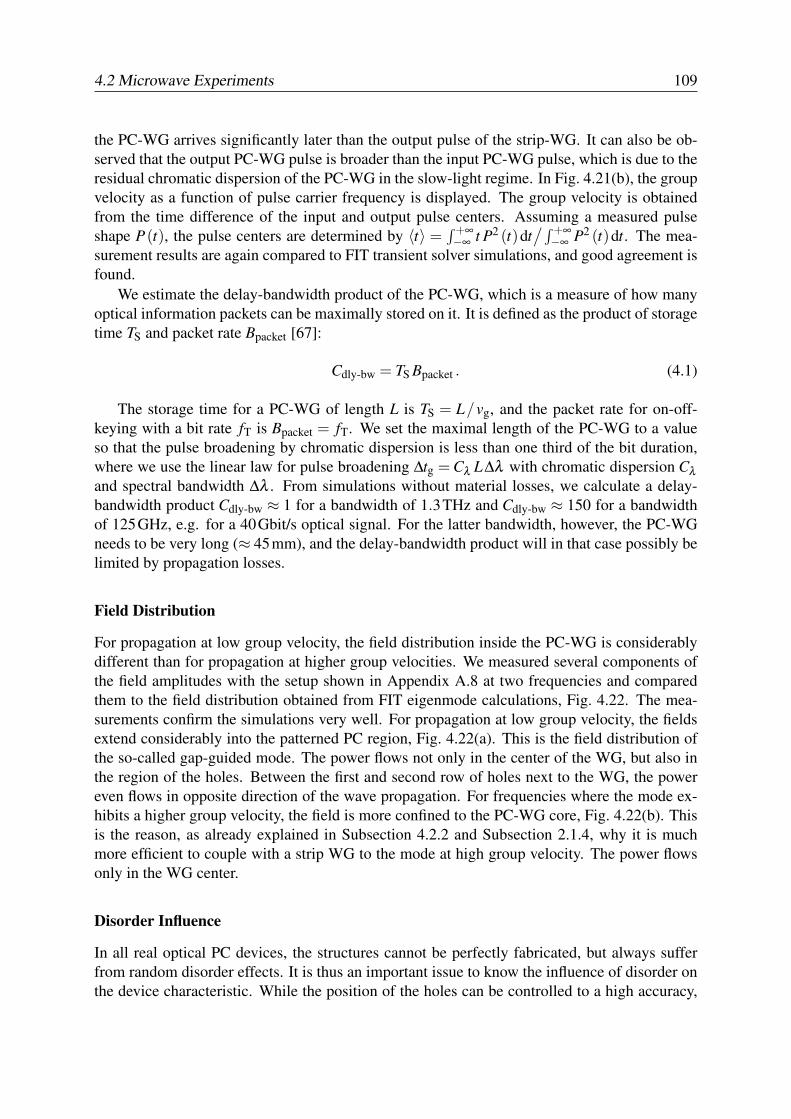
4.2 Microwave Experiments 109
the PC-WG arrives significantly later than the output pulse of the strip-WG. It can also be ob-served that the output PC-WG pulse is broader than the input PC-WG pulse, which is due to theresidual chromatic dispersion of the PC-WG in the slow-light regime. In Fig. 4.21(b), the groupvelocity as a function of pulse carrier frequency is displayed. The group velocity is obtainedfrom the time difference of the input and output pulse centers. Assuming a measured pulseshape P(t), the pulse centers are determined by 〈t〉 =
∫ +∞−∞ t P2 (t)dt
/∫ +∞−∞ P2 (t)dt. The mea-
surement results are again compared to FIT transient solver simulations, and good agreement isfound.
We estimate the delay-bandwidth product of the PC-WG, which is a measure of how manyoptical information packets can be maximally stored on it. It is defined as the product of storagetime TS and packet rate Bpacket [67]:
Cdly-bw = TS Bpacket . (4.1)
The storage time for a PC-WG of length L is TS = L/vg, and the packet rate for on-off-keying with a bit rate fT is Bpacket = fT. We set the maximal length of the PC-WG to a valueso that the pulse broadening by chromatic dispersion is less than one third of the bit duration,where we use the linear law for pulse broadening ∆tg = Cλ L∆λ with chromatic dispersion Cλand spectral bandwidth ∆λ . From simulations without material losses, we calculate a delay-bandwidth product Cdly-bw ≈ 1 for a bandwidth of 1.3THz and Cdly-bw ≈ 150 for a bandwidthof 125GHz, e.g. for a 40Gbit/s optical signal. For the latter bandwidth, however, the PC-WGneeds to be very long (≈ 45mm), and the delay-bandwidth product will in that case possibly belimited by propagation losses.
Field Distribution
For propagation at low group velocity, the field distribution inside the PC-WG is considerablydifferent than for propagation at higher group velocities. We measured several components ofthe field amplitudes with the setup shown in Appendix A.8 at two frequencies and comparedthem to the field distribution obtained from FIT eigenmode calculations, Fig. 4.22. The mea-surements confirm the simulations very well. For propagation at low group velocity, the fieldsextend considerably into the patterned PC region, Fig. 4.22(a). This is the field distribution ofthe so-called gap-guided mode. The power flows not only in the center of the WG, but also inthe region of the holes. Between the first and second row of holes next to the WG, the powereven flows in opposite direction of the wave propagation. For frequencies where the mode ex-hibits a higher group velocity, the field is more confined to the PC-WG core, Fig. 4.22(b). Thisis the reason, as already explained in Subsection 4.2.2 and Subsection 2.1.4, why it is muchmore efficient to couple with a strip WG to the mode at high group velocity. The power flowsonly in the WG center.
Disorder Influence
In all real optical PC devices, the structures cannot be perfectly fabricated, but always sufferfrom random disorder effects. It is thus an important issue to know the influence of disorder onthe device characteristic. While the position of the holes can be controlled to a high accuracy,
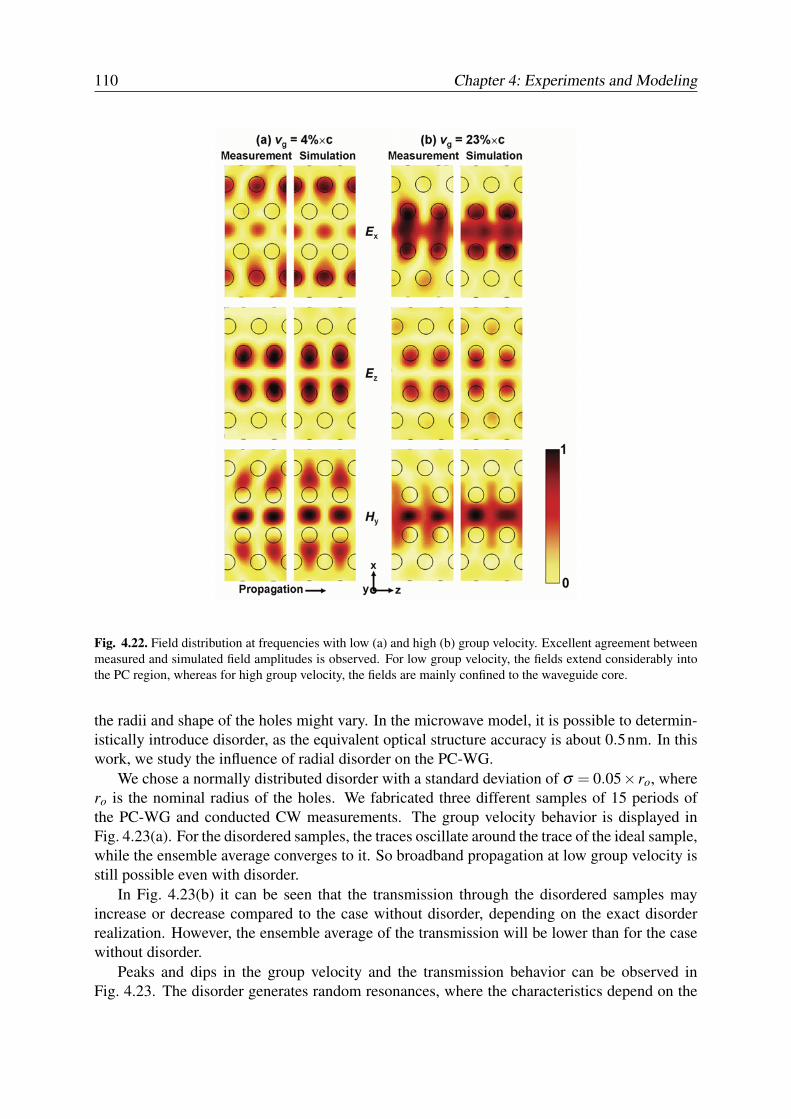
110 Chapter 4: Experiments and Modeling
Fig. 4.22. Field distribution at frequencies with low (a) and high (b) group velocity. Excellent agreement betweenmeasured and simulated field amplitudes is observed. For low group velocity, the fields extend considerably intothe PC region, whereas for high group velocity, the fields are mainly confined to the waveguide core.
the radii and shape of the holes might vary. In the microwave model, it is possible to determin-istically introduce disorder, as the equivalent optical structure accuracy is about 0.5nm. In thiswork, we study the influence of radial disorder on the PC-WG.
We chose a normally distributed disorder with a standard deviation of σ = 0.05× ro, wherero is the nominal radius of the holes. We fabricated three different samples of 15 periods ofthe PC-WG and conducted CW measurements. The group velocity behavior is displayed inFig. 4.23(a). For the disordered samples, the traces oscillate around the trace of the ideal sample,while the ensemble average converges to it. So broadband propagation at low group velocity isstill possible even with disorder.
In Fig. 4.23(b) it can be seen that the transmission through the disordered samples mayincrease or decrease compared to the case without disorder, depending on the exact disorderrealization. However, the ensemble average of the transmission will be lower than for the casewithout disorder.
Peaks and dips in the group velocity and the transmission behavior can be observed inFig. 4.23. The disorder generates random resonances, where the characteristics depend on the
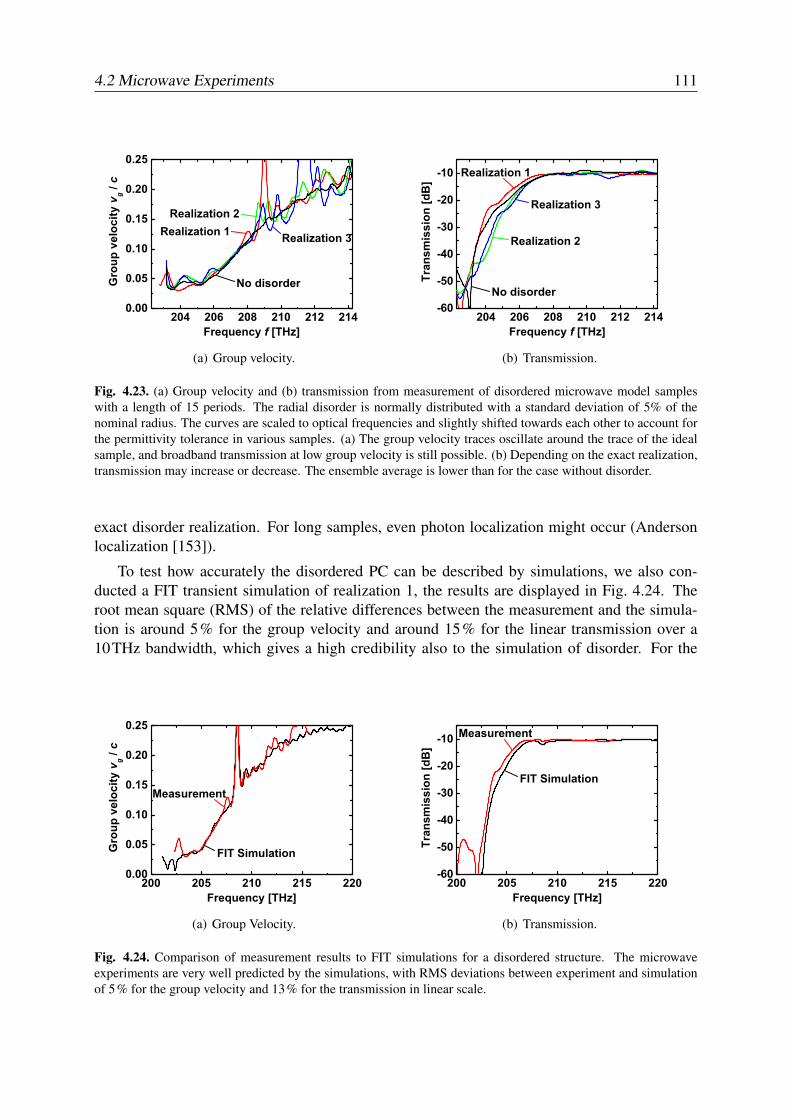
4.2 Microwave Experiments 111
204 206 208 210 212 2140.00
0.05
0.10
0.15
0.20
0.25
Realization 3
Realization 2Realization 1
Gro
up v
eloc
ity v
g / c
Frequency f [THz]
No disorder
(a) Group velocity.
204 206 208 210 212 214-60
-50
-40
-30
-20
-10
Tran
smis
sion
[dB
]
Frequency f [THz]
Realization 3
Realization 2
Realization 1
No disorder
(b) Transmission.
Fig. 4.23. (a) Group velocity and (b) transmission from measurement of disordered microwave model sampleswith a length of 15 periods. The radial disorder is normally distributed with a standard deviation of 5% of thenominal radius. The curves are scaled to optical frequencies and slightly shifted towards each other to account forthe permittivity tolerance in various samples. (a) The group velocity traces oscillate around the trace of the idealsample, and broadband transmission at low group velocity is still possible. (b) Depending on the exact realization,transmission may increase or decrease. The ensemble average is lower than for the case without disorder.
exact disorder realization. For long samples, even photon localization might occur (Andersonlocalization [153]).
To test how accurately the disordered PC can be described by simulations, we also con-ducted a FIT transient simulation of realization 1, the results are displayed in Fig. 4.24. Theroot mean square (RMS) of the relative differences between the measurement and the simula-tion is around 5% for the group velocity and around 15% for the linear transmission over a10THz bandwidth, which gives a high credibility also to the simulation of disorder. For the
200 205 210 215 2200.00
0.05
0.10
0.15
0.20
0.25
Measurement
Gro
up v
eloc
ity v
g / c
Frequency [THz]
FIT Simulation
(a) Group Velocity.
200 205 210 215 220-60
-50
-40
-30
-20
-10
Tran
smis
sion
[dB
]
Frequency [THz]
FIT Simulation
Measurement
(b) Transmission.
Fig. 4.24. Comparison of measurement results to FIT simulations for a disordered structure. The microwaveexperiments are very well predicted by the simulations, with RMS deviations between experiment and simulationof 5% for the group velocity and 13% for the transmission in linear scale.
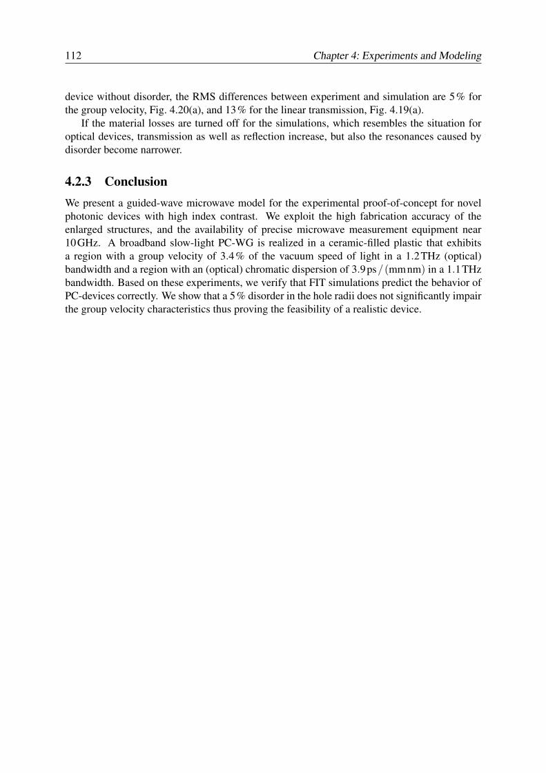
112 Chapter 4: Experiments and Modeling
device without disorder, the RMS differences between experiment and simulation are 5% forthe group velocity, Fig. 4.20(a), and 13% for the linear transmission, Fig. 4.19(a).
If the material losses are turned off for the simulations, which resembles the situation foroptical devices, transmission as well as reflection increase, but also the resonances caused bydisorder become narrower.
4.2.3 ConclusionWe present a guided-wave microwave model for the experimental proof-of-concept for novelphotonic devices with high index contrast. We exploit the high fabrication accuracy of theenlarged structures, and the availability of precise microwave measurement equipment near10GHz. A broadband slow-light PC-WG is realized in a ceramic-filled plastic that exhibitsa region with a group velocity of 3.4% of the vacuum speed of light in a 1.2THz (optical)bandwidth and a region with an (optical) chromatic dispersion of 3.9ps/(mmnm) in a 1.1THzbandwidth. Based on these experiments, we verify that FIT simulations predict the behavior ofPC-devices correctly. We show that a 5% disorder in the hole radii does not significantly impairthe group velocity characteristics thus proving the feasibility of a realistic device.
4.3 Verification of Numerics 113
4.3 Verification of Numerics
The first step in the process to build functional integrated PC devices is the numerical designof the PC-WG, which is done with band calculations, as presented in Section 2.1. Various nu-merical methods are available and commonly used to achieve the design, yet not all are equallyfeasible, and considerable differences in simulation time and hardware requirements exist. Af-ter the design of the PC-WGs, also complete devices need to be simulated to gain better insightsinto the device behavior and to avoid unneeded fabrication runs. In Section 4.2, it has also beenverified that the FIT method can well predict the behavior a PC-WG device including couplingsections and the transition from strip-WG to PC-WG, even in the presence of systematically in-troduced radial disorder. The microwave material, however, exhibits significant material losses,which are not present in silicon or glass, and the behavior especially of disordered structuresmight become different if the material losses become negligible.
In this section, we evaluate several methods for band calculations, which are the FIT, FDTD,PWE and GME methods. As has been already presented in Section 4.2, the FIT method ac-curately predicts the measured group velocity and chromatic dispersion behavior of a scaledPC-WG in the microwave regime. We find that the GME method is a very fast design tool thatpredicts the PC-WG behavior correctly. Furthermore, we study the feasibility of the FIT, GMEand FDTD methods to determine the influence of disorder on the silicon device characteristics,as needed for the work presented in Section 2.2. We find that the results from FIT and FDTDare trustworthy, whereas the GME method needs to be used more carefully.
This section is organized as follows: In Subsection 4.3.1, different design tools are bench-marked, and in Subsection 4.3.2, the numerics verification to study disordered PC-WG is pre-sented.
The contents of Subsection 4.3.1 have been published as part of a journal article, [2] or [J2]on page 165.
4.3.1 Benchmark of Different Design Tools
A PC-WG with a certain group velocity or dispersion characteristic is designed with numeri-cal band calculations. To choose among the different numerical methods, accuracy, calculationspeed and memory requirements have to be evaluated. For the slow-light PC-WG, we bench-mark the four different methods mentioned in Appendix A.2, namely the FIT eigenmode solver,FDTD, PWE and GME methods. Fig. 4.25 shows the group velocity curves obtained from theband diagrams. The curves from FIT eigenmode, PWE and GME solver are almost identicaland predict the behavior of the component correctly, as verified by microwave experiments,Fig. 4.20(a). The FDTD curve, however, is shifted in frequency and deviates more from theother results.
In Table 4.2, the simulation runtime for 20 wavevector points of the band diagram and thememory usage of the different methods are compared. For the simulations, a discretization ofaround 20 cells per period and symmetric boundary conditions were used. The FIT eigenmode,FDTD and GME simulations were run on a standard computer, whereas the PWE simulationswere run on 12 nodes of a unix cluster, as the memory size of a single computer was notsufficient.
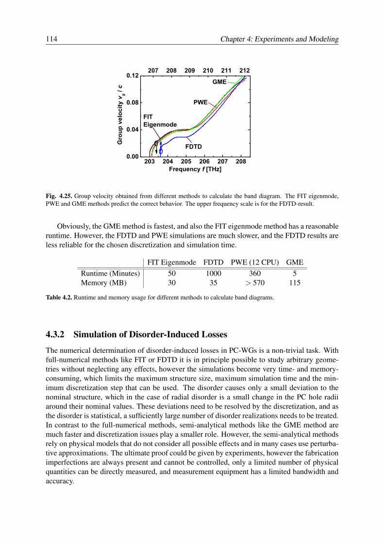
114 Chapter 4: Experiments and Modeling
203 204 205 206 207 2080.00
0.04
0.08
0.12207 208 209 210 211 212
GME
FIT Eigenmode
PWE
Gro
up v
eloc
ity v
g / c
Frequency f [THz]
FDTD
Fig. 4.25. Group velocity obtained from different methods to calculate the band diagram. The FIT eigenmode,PWE and GME methods predict the correct behavior. The upper frequency scale is for the FDTD-result.
Obviously, the GME method is fastest, and also the FIT eigenmode method has a reasonableruntime. However, the FDTD and PWE simulations are much slower, and the FDTD results areless reliable for the chosen discretization and simulation time.
FIT Eigenmode FDTD PWE (12 CPU) GMERuntime (Minutes) 50 1000 360 5Memory (MB) 30 35 > 570 115
Table 4.2. Runtime and memory usage for different methods to calculate band diagrams.
4.3.2 Simulation of Disorder-Induced Losses
The numerical determination of disorder-induced losses in PC-WGs is a non-trivial task. Withfull-numerical methods like FIT or FDTD it is in principle possible to study arbitrary geome-tries without neglecting any effects, however the simulations become very time- and memory-consuming, which limits the maximum structure size, maximum simulation time and the min-imum discretization step that can be used. The disorder causes only a small deviation to thenominal structure, which in the case of radial disorder is a small change in the PC hole radiiaround their nominal values. These deviations need to be resolved by the discretization, and asthe disorder is statistical, a sufficiently large number of disorder realizations needs to be treated.In contrast to the full-numerical methods, semi-analytical methods like the GME method aremuch faster and discretization issues play a smaller role. However, the semi-analytical methodsrely on physical models that do not consider all possible effects and in many cases use perturba-tive approximations. The ultimate proof could be given by experiments, however the fabricationimperfections are always present and cannot be controlled, only a limited number of physicalquantities can be directly measured, and measurement equipment has a limited bandwidth andaccuracy.
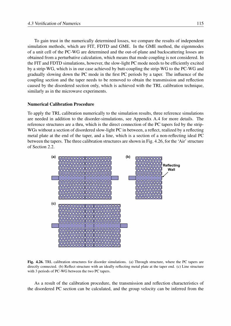
4.3 Verification of Numerics 115
To gain trust in the numerically determined losses, we compare the results of independentsimulation methods, which are FIT, FDTD and GME. In the GME method, the eigenmodesof a unit cell of the PC-WG are determined and the out-of-plane and backscattering losses areobtained from a perturbative calculation, which means that mode coupling is not considered. Inthe FIT and FDTD simulations, however, the slow-light PC mode needs to be efficiently excitedby a strip-WG, which is in our case achieved by butt-coupling the strip-WG to the PC-WG andgradually slowing down the PC mode in the first PC periods by a taper. The influence of thecoupling section and the taper needs to be removed to obtain the transmission and reflectioncaused by the disordered section only, which is achieved with the TRL calibration technique,similarly as in the microwave experiments.
Numerical Calibration Procedure
To apply the TRL calibration numerically to the simulation results, three reference simulationsare needed in addition to the disorder-simulations, see Appendix A.4 for more details. Thereference structures are a thru, which is the direct connection of the PC tapers fed by the strip-WGs without a section of disordered slow-light PC in between, a reflect, realized by a reflectingmetal plate at the end of the taper, and a line, which is a section of a non-reflecting ideal PCbetween the tapers. The three calibration structures are shown in Fig. 4.26, for the ‘Air’ structureof Section 2.2.
Fig. 4.26. TRL calibration structures for disorder simulations. (a) Through structure, where the PC tapers aredirectly connected. (b) Reflect structure with an ideally reflecting metal plate at the taper end. (c) Line structurewith 3 periods of PC-WG between the two PC tapers.
As a result of the calibration procedure, the transmission and reflection characteristics ofthe disordered PC section can be calculated, and the group velocity can be inferred from the
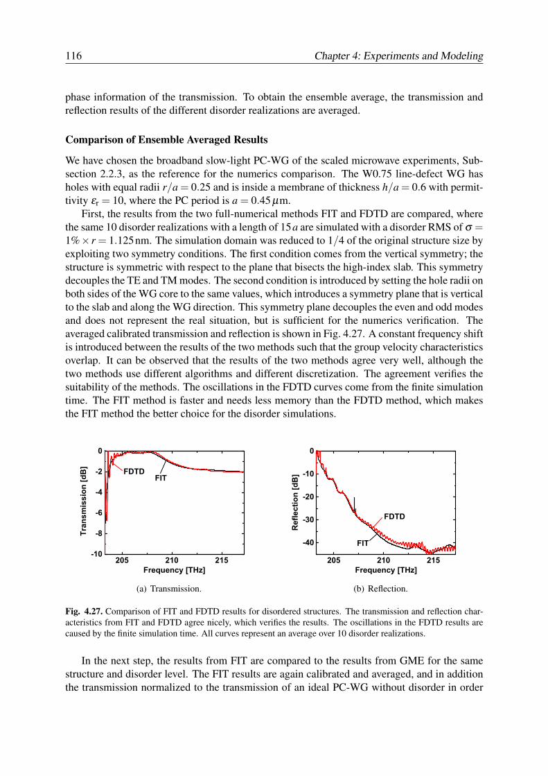
116 Chapter 4: Experiments and Modeling
phase information of the transmission. To obtain the ensemble average, the transmission andreflection results of the different disorder realizations are averaged.
Comparison of Ensemble Averaged Results
We have chosen the broadband slow-light PC-WG of the scaled microwave experiments, Sub-section 2.2.3, as the reference for the numerics comparison. The W0.75 line-defect WG hasholes with equal radii r/a = 0.25 and is inside a membrane of thickness h/a = 0.6 with permit-tivity εr = 10, where the PC period is a = 0.45 µm.
First, the results from the two full-numerical methods FIT and FDTD are compared, wherethe same 10 disorder realizations with a length of 15a are simulated with a disorder RMS of σ =1%× r = 1.125nm. The simulation domain was reduced to 1/4 of the original structure size byexploiting two symmetry conditions. The first condition comes from the vertical symmetry; thestructure is symmetric with respect to the plane that bisects the high-index slab. This symmetrydecouples the TE and TM modes. The second condition is introduced by setting the hole radii onboth sides of the WG core to the same values, which introduces a symmetry plane that is verticalto the slab and along the WG direction. This symmetry plane decouples the even and odd modesand does not represent the real situation, but is sufficient for the numerics verification. Theaveraged calibrated transmission and reflection is shown in Fig. 4.27. A constant frequency shiftis introduced between the results of the two methods such that the group velocity characteristicsoverlap. It can be observed that the results of the two methods agree very well, although thetwo methods use different algorithms and different discretization. The agreement verifies thesuitability of the methods. The oscillations in the FDTD curves come from the finite simulationtime. The FIT method is faster and needs less memory than the FDTD method, which makesthe FIT method the better choice for the disorder simulations.
205 210 215-10
-8
-6
-4
-2
0
FDTD
Tran
smis
sion
[dB
]
Frequency [THz]
FIT
(a) Transmission.
205 210 215
-40
-30
-20
-10
0
FDTD
Ref
lect
ion
[dB
]
Frequency [THz]
FIT
(b) Reflection.
Fig. 4.27. Comparison of FIT and FDTD results for disordered structures. The transmission and reflection char-acteristics from FIT and FDTD agree nicely, which verifies the results. The oscillations in the FDTD results arecaused by the finite simulation time. All curves represent an average over 10 disorder realizations.
In the next step, the results from FIT are compared to the results from GME for the samestructure and disorder level. The FIT results are again calibrated and averaged, and in additionthe transmission normalized to the transmission of an ideal PC-WG without disorder in order
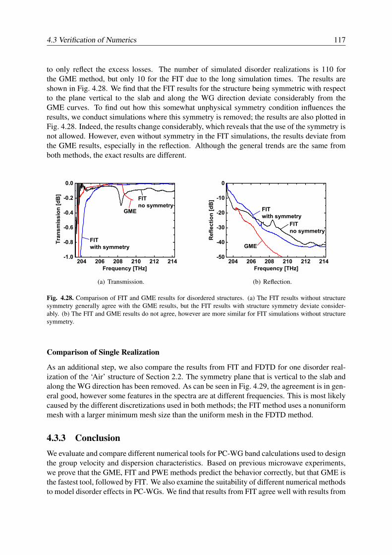
4.3 Verification of Numerics 117
to only reflect the excess losses. The number of simulated disorder realizations is 110 forthe GME method, but only 10 for the FIT due to the long simulation times. The results areshown in Fig. 4.28. We find that the FIT results for the structure being symmetric with respectto the plane vertical to the slab and along the WG direction deviate considerably from theGME curves. To find out how this somewhat unphysical symmetry condition influences theresults, we conduct simulations where this symmetry is removed; the results are also plotted inFig. 4.28. Indeed, the results change considerably, which reveals that the use of the symmetry isnot allowed. However, even without symmetry in the FIT simulations, the results deviate fromthe GME results, especially in the reflection. Although the general trends are the same fromboth methods, the exact results are different.
204 206 208 210 212 214-1.0
-0.8
-0.6
-0.4
-0.2
0.0
FITwith symmetry
Tran
smis
sion
[dB
]
Frequency [THz]
FITno symmetry
GME
(a) Transmission.
204 206 208 210 212 214-50
-40
-30
-20
-10
0
Ref
lect
ion
[dB
]
Frequency [THz]
GME
FITno symmetry
FITwith symmetry
(b) Reflection.
Fig. 4.28. Comparison of FIT and GME results for disordered structures. (a) The FIT results without structuresymmetry generally agree with the GME results, but the FIT results with structure symmetry deviate consider-ably. (b) The FIT and GME results do not agree, however are more similar for FIT simulations without structuresymmetry.
Comparison of Single Realization
As an additional step, we also compare the results from FIT and FDTD for one disorder real-ization of the ‘Air’ structure of Section 2.2. The symmetry plane that is vertical to the slab andalong the WG direction has been removed. As can be seen in Fig. 4.29, the agreement is in gen-eral good, however some features in the spectra are at different frequencies. This is most likelycaused by the different discretizations used in both methods; the FIT method uses a nonuniformmesh with a larger minimum mesh size than the uniform mesh in the FDTD method.
4.3.3 ConclusionWe evaluate and compare different numerical tools for PC-WG band calculations used to designthe group velocity and dispersion characteristics. Based on previous microwave experiments,we prove that the GME, FIT and PWE methods predict the behavior correctly, but that GME isthe fastest tool, followed by FIT. We also examine the suitability of different numerical methodsto model disorder effects in PC-WGs. We find that results from FIT agree well with results from
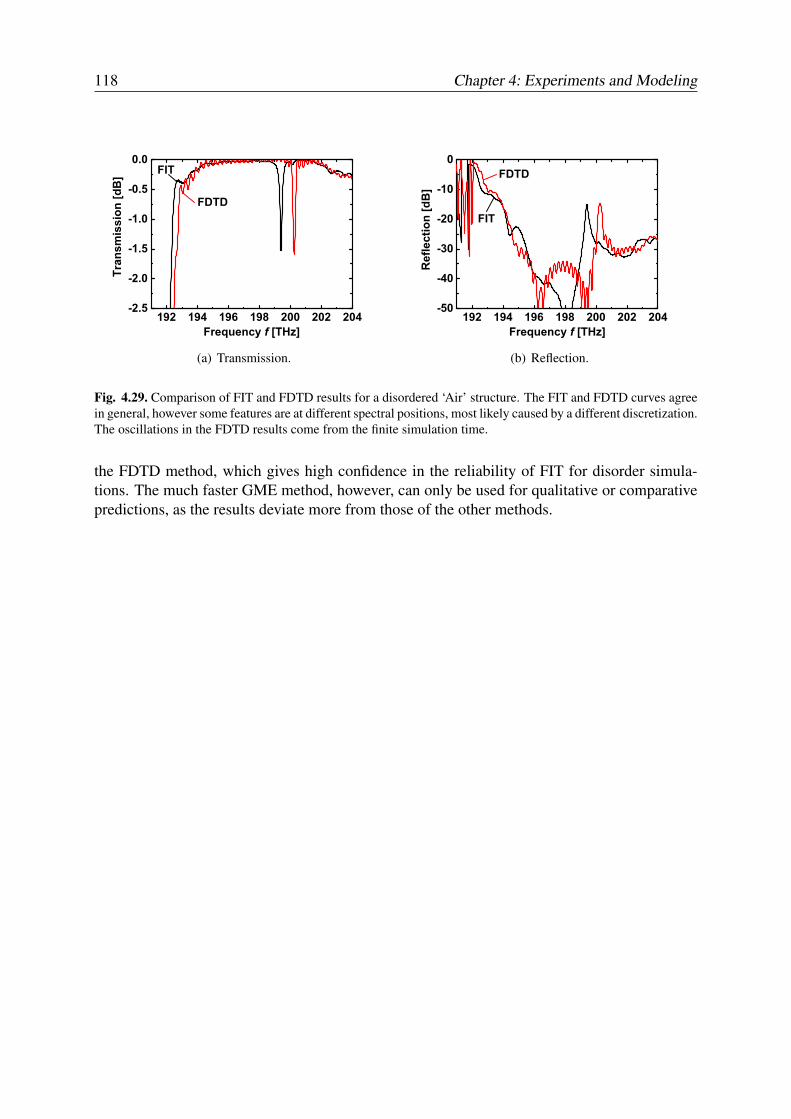
118 Chapter 4: Experiments and Modeling
192 194 196 198 200 202 204-2.5
-2.0
-1.5
-1.0
-0.5
0.0
Tran
smis
sion
[dB
]
Frequency f [THz]
FDTD
FIT
(a) Transmission.
192 194 196 198 200 202 204-50
-40
-30
-20
-10
0
Ref
lect
ion
[dB
]
Frequency f [THz]
FDTD
FIT
(b) Reflection.
Fig. 4.29. Comparison of FIT and FDTD results for a disordered ‘Air’ structure. The FIT and FDTD curves agreein general, however some features are at different spectral positions, most likely caused by a different discretization.The oscillations in the FDTD results come from the finite simulation time.
the FDTD method, which gives high confidence in the reliability of FIT for disorder simula-tions. The much faster GME method, however, can only be used for qualitative or comparativepredictions, as the results deviate more from those of the other methods.
Appendix
A.1 Mathematical Transformations and Signal Representa-tion
In this section, we briefly state the mathematical transformations and the signal representationused in the thesis.
A.1.1 Fourier Transform
A signal or linear system response can be represented in time domain as a function of time x(t),or in frequency domain as a function of frequency X ( f ). The transformation from time-domaininto frequency-domain is accomplished with the Fourier transform, and the transformation fromfrequency-domain into time-domain with the inverse Fourier transform. The relations are:
X ( f ) =∫ +∞
−∞x(t)e− j2π f t dt , (A.1)
x(t) =∫ +∞
−∞X ( f )e j2π f t d f . (A.2)
In addition to the time-frequency Fourier transform, an analog three-dimensional spatial Fouriertransform can be defined that transforms a function dependent on spatial coordinates into thewavevector space, where the function is expanded into plane waves, and vice versa.
A.1.2 Signal Representation
Throughout this work, we represent optical signals and fields as complex quantities. The time-dependence of the carrier is of the form e jωt , and the propagation along a WG in z−directioncan be expressed as e− jβ z. The measurable physical quantities of the fields correspond to thereal part of the complex representation. The complex functions are analytical, and the imagi-nary part of the function is obtained as the Hilbert transform of the real part. If the analyticalfunction is represented in the frequency domain by using the Fourier transform, only spectralcomponents at positive frequencies exist, whereas the Fourier transform of the correspondingreal function has components at positive and negative frequencies, and the components at neg-ative frequencies are the complex conjugate values of the components at positive frequenciesmirrored at the origin.
119
120 Appendix
The reponse y(t) of a signal x(t) transmitted through a linear time-invariant system withimpulse response g(t) can be calculated as the convolution of the input signal and the impulseresponse:
y(t) = x(t)∗g(t) =∫ +∞
−∞x(τ) g(t− τ)dτ . (A.3)
In frequency domain, the spectrum Y ( f ) of the output signal y(t) can be obtained by multiply-ing the spectrum X ( f ) of the input signal x(t) with the Fourier transform G( f ) of the impulseresponse g(t):
Y ( f ) = X ( f ) G( f ) . (A.4)
The function G( f ) is also called the transfer function of the system. The properties of a linearoptical device can be characterized with its S−parameters as a function of frequency, Eq. (A.24),and the device transfer functions for the transmitted or reflected signals are just the correspond-ing S−parameters, S21 ( f ) or S11 ( f ), respectively.
If a system is excited with a harmonic x(t) = A exp(j2π f0t) of complex amplitude A andfrequency f0, the output signal is just the input signal multiplied with the transfer function atfrequency f0, y(t) = G( f0) A exp(j2π f0t).
A.1.3 Laplace TransformThe Laplace transform maps a causal function x(t) into the complex s−space. The transforma-tion equations are:
X (s) =∫ +∞
0y(t)e−st dt , (A.5)
x(t) =1
j2π
∫ c+j∞
c−j∞Y (s)est ds . (A.6)
The Laplace transform can e. g. be used to solve differential equations, where correspondencetables can be consulted to transform the functions. Correpondence pairs are denoted in the formx(t)−•X (s). In Appendix A.6, we use the Laplace transform to solve the differential equationsof the loss model.
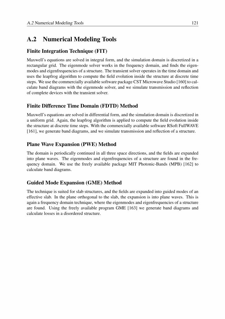
A.2 Numerical Modeling Tools 121
A.2 Numerical Modeling Tools
Finite Integration Technique (FIT)Maxwell’s equations are solved in integral form, and the simulation domain is discretized in arectangular grid. The eigenmode solver works in the frequency domain, and finds the eigen-modes and eigenfrequencies of a structure. The transient solver operates in the time domain anduses the leapfrog algorithm to compute the field evolution inside the structure at discrete timesteps. We use the commercially available software package CST Microwave Studio [160] to cal-culate band diagrams with the eigenmode solver, and we simulate transmission and reflectionof complete devices with the transient solver.
Finite Difference Time Domain (FDTD) MethodMaxwell’s equations are solved in differential form, and the simulation domain is discretized ina uniform grid. Again, the leapfrog algorithm is applied to compute the field evolution insidethe structure at discrete time steps. With the commercially available software RSoft FullWAVE[161], we generate band diagrams, and we simulate transmission and reflection of a structure.
Plane Wave Expansion (PWE) MethodThe domain is periodically continued in all three space directions, and the fields are expandedinto plane waves. The eigenmodes and eigenfrequencies of a structure are found in the fre-quency domain. We use the freely available package MIT Photonic-Bands (MPB) [162] tocalculate band diagrams.
Guided Mode Expansion (GME) MethodThe technique is suited for slab structures, and the fields are expanded into guided modes of aneffective slab. In the plane orthogonal to the slab, the expansion is into plane waves. This isagain a frequency domain technique, where the eigenmodes and eigenfrequencies of a structureare found. Using the freely available program GME [163] we generate band diagrams andcalculate losses in a disordered structure.

122 Appendix
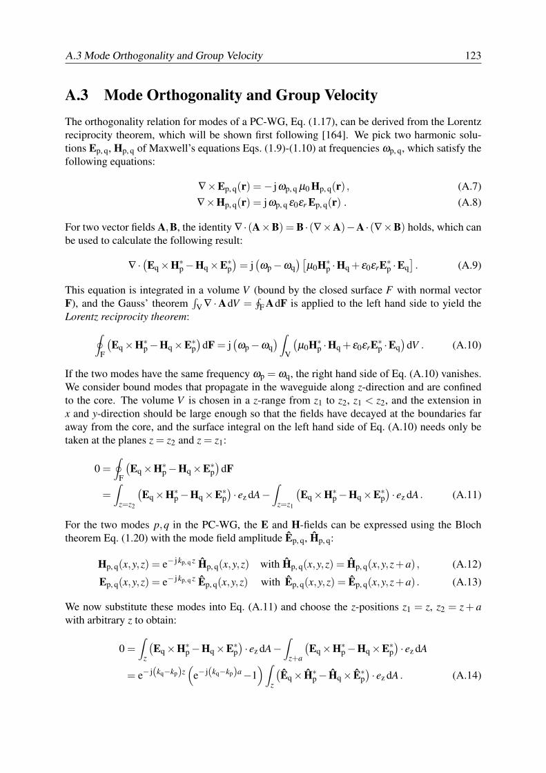
A.3 Mode Orthogonality and Group Velocity 123
A.3 Mode Orthogonality and Group VelocityThe orthogonality relation for modes of a PC-WG, Eq. (1.17), can be derived from the Lorentzreciprocity theorem, which will be shown first following [164]. We pick two harmonic solu-tions Ep, q, Hp, q of Maxwell’s equations Eqs. (1.9)-(1.10) at frequencies ωp, q, which satisfy thefollowing equations:
∇×Ep, q(r) =− jωp, q µ0 Hp, q(r) , (A.7)∇×Hp, q(r) = jωp, q ε0εr Ep, q(r) . (A.8)
For two vector fields A,B, the identity ∇ · (A×B) = B · (∇×A)−A · (∇×B) holds, which canbe used to calculate the following result:
∇ · (Eq×H∗p−Hq×E∗p
)= j
(ωp−ωq
)[µ0H∗
p ·Hq + ε0εrE∗p ·Eq]. (A.9)
This equation is integrated in a volume V (bound by the closed surface F with normal vectorF), and the Gauss’ theorem
∫V ∇ ·AdV =
∮F AdF is applied to the left hand side to yield the
Lorentz reciprocity theorem:∮
F
(Eq×H∗
p−Hq×E∗p)
dF = j(ωp−ωq
)∫
V
(µ0H∗
p ·Hq + ε0εrE∗p ·Eq)
dV . (A.10)
If the two modes have the same frequency ωp = ωq, the right hand side of Eq. (A.10) vanishes.We consider bound modes that propagate in the waveguide along z-direction and are confinedto the core. The volume V is chosen in a z-range from z1 to z2, z1 < z2, and the extension inx and y-direction should be large enough so that the fields have decayed at the boundaries faraway from the core, and the surface integral on the left hand side of Eq. (A.10) needs only betaken at the planes z = z2 and z = z1:
0 =∮
F
(Eq×H∗
p−Hq×E∗p)
dF
=∫
z=z2
(Eq×H∗
p−Hq×E∗p) · ez dA−
∫
z=z1
(Eq×H∗
p−Hq×E∗p) · ez dA . (A.11)
For the two modes p,q in the PC-WG, the E and H-fields can be expressed using the Blochtheorem Eq. (1.20) with the mode field amplitude Ep, q, Hp, q:
Hp, q(x,y,z) = e− jkp, q z Hp, q(x,y,z) with Hp, q(x,y,z) = Hp, q(x,y,z+a) , (A.12)
Ep, q(x,y,z) = e− jkp, q z Ep, q(x,y,z) with Ep, q(x,y,z) = Ep, q(x,y,z+a) . (A.13)
We now substitute these modes into Eq. (A.11) and choose the z-positions z1 = z, z2 = z + awith arbitrary z to obtain:
0 =∫
z
(Eq×H∗
p−Hq×E∗p) · ez dA−
∫
z+a
(Eq×H∗
p−Hq×E∗p) · ez dA
= e− j(kq−kp)z(
e− j(kq−kp)a−1)∫
z
(Eq× H∗
p− Hq× E∗p) · ez dA . (A.14)
124 Appendix
In the second line of this equation, either the factor(
e− j(kq−kp)a−1)
or the integral expression∫
z(Eq× H∗
p− Hq× E∗p) · ez dA has to vanish for the equation to hold. This leads to the mode
orthogonality relation for PC-WGs (kp, q is inside the first Brillouin zone −π/a . . .π/a):∫
z
(Eq× H∗
p− Hq× E∗p) · ez dA = 4δp, q Pp . (A.15)
Here, δp, q is the Kronecker delta, and Pp is the cross-section power of mode p. For p = q, thepower of the mode is obtained
Pp =14
∫
z
(Eq× H∗
q− Hq× E∗q) · ez dA =
12
∫
zℜ
(Eq× H∗
q) · ez dA , (A.16)
where the conversion on the right hand side was achieved using the identities −Hq × E∗q =E∗q× Hq and w + w∗ = 2ℜ(w) for a complex number w. On the right-hand side of Eq. (A.16),the Poynting vector S = 1
2E× H∗ appears, and the real part of its z-component specifies thepower flow in propagation direction. If integrated over a cross-section area, the total power isobtained, which is constant along z if no losses occur.
From the mode field distribution, it is also possible to infer the group velocity vg = dωdk of
the mode. This can be derived starting from Lorentz reciprocity theorem, Eq. (A.10), but withinitially different frequencies for the two modes p and q [164]. Then, the same steps as aboveare followed and the PC-WG modes Eqs. (A.12)-(A.13) substituted, which results in a moregeneral relation of Eq. (A.14) with a non-vanishing left hand side (the position z can withoutloss of generality be chosen as 0 by just shifting the structure):
j(ωp−ωq
)∫
V
(µ0H∗
p · Hq + ε0εrE∗p · Eq)
dV
=(
e− j(kq−kp)a−1)∫
z
(Eq× H∗
p− Hq× E∗p) · ez dA . (A.17)
If the same mode is chosen for p and q and the frequency ωq approaches ωq, the mode fieldsbecome the same, Ep = Eq = E, Hp = Hq = H, and a differential is obtained (where e− j(kq−kp)a
becomes 1):
− jdω∫
V
(µ0
∣∣H∣∣2
+ ε0εr∣∣E
∣∣2)
dV =− jadk∫
z
(E× H∗− H× E∗
) · ez dA . (A.18)
From this equation, the group velocity can be inferred:
vg =dωdk
=a
∫z(E× H∗− H× E∗
) · ez dA∫
V
(µ0
∣∣H∣∣2
+ ε0εr∣∣E
∣∣2)
dV=
2a∫
z ℜ(E× H∗) · ez dA
∫V
(µ0
∣∣H∣∣2
+ ε0εr∣∣E
∣∣2)
dV. (A.19)
The surface integral in the numerator is performed over a cross-section orthogonal to propaga-tion direction, and the volume integration in the denominator is over a unit cell of the PC oflength a. The integrand in the numerator is the real part of the Poynting vector in z−direction,and the integral quantifies the total power flow of the mode. In the denominator, the integrand
A.3 Mode Orthogonality and Group Velocity 125
is the sum of the magnetic and electric energy density in the unit cell. Thus, for a fixed amountof transmitted power, the stored energy increases inversely proportional to the group velocity ofa mode.
It can be shown that the integral of the electric and magnetic energy density over a unit cellare same, which will be proven in the following. With the same procedure that led to Eq. (A.9),it can be shown that a solution of Maxwell’s equations satisfies
∇ · (E×H∗) = jω(
ε0εr |E|2−µ0 |H|2)
. (A.20)
The Gauss’ theorem (as stated after Eq. (A.9) can be applied to this equation, and results in
jω∫
V
(ε0εr |E|2−µ0 |H|2
)dV =
∮
F(E×H∗)dF . (A.21)
If a PC mode according to Eqs. (A.12)-(A.13) is substituted in Eq. (A.21) and the volume V ischosen as a PC unit cell from z1 = z to z2 = z+a, the surface integral over the closed surface Fcan be represented as a sum of two surface integrals at the constant z-planes at z and z+a:
jω∫
V
(ε0εr
∣∣E∣∣2−µ0
∣∣H∣∣2
)dV =
∫
z+a(E×H∗) · ez dA−
∫
z(E×H∗) · ez dA
=∫
z+a
(E× H∗) · ez dA−
∫
z
(E× H∗) · ez dA
= 0 , (A.22)
which results in the equality of the electric and magnetic energy density integrated in a unit cellV : ∫
Vε0εr
∣∣E∣∣2
dV =∫
Vµ0
∣∣H∣∣2
dV . (A.23)
This equality can be used in Eq. (A.19) to simplify the calculation in the denominator.

126 Appendix
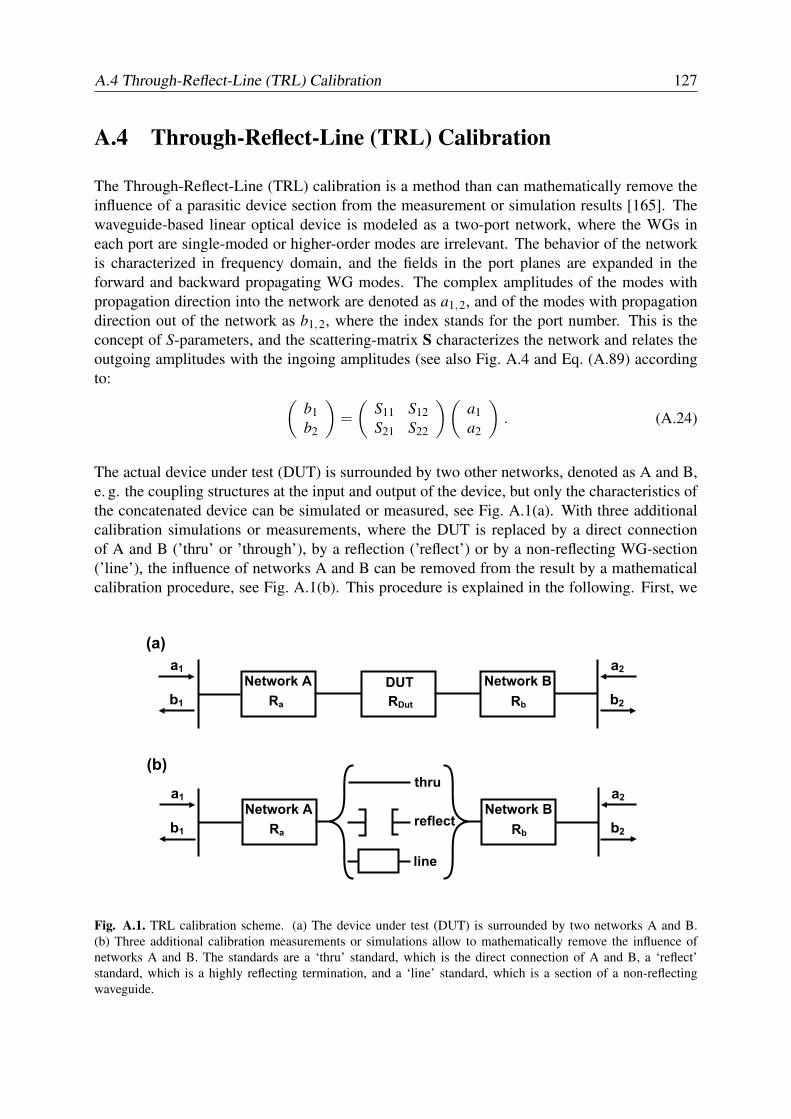
A.4 Through-Reflect-Line (TRL) Calibration 127
A.4 Through-Reflect-Line (TRL) Calibration
The Through-Reflect-Line (TRL) calibration is a method than can mathematically remove theinfluence of a parasitic device section from the measurement or simulation results [165]. Thewaveguide-based linear optical device is modeled as a two-port network, where the WGs ineach port are single-moded or higher-order modes are irrelevant. The behavior of the networkis characterized in frequency domain, and the fields in the port planes are expanded in theforward and backward propagating WG modes. The complex amplitudes of the modes withpropagation direction into the network are denoted as a1,2, and of the modes with propagationdirection out of the network as b1,2, where the index stands for the port number. This is theconcept of S-parameters, and the scattering-matrix S characterizes the network and relates theoutgoing amplitudes with the ingoing amplitudes (see also Fig. A.4 and Eq. (A.89) accordingto:
(b1b2
)=
(S11 S12S21 S22
)(a1a2
). (A.24)
The actual device under test (DUT) is surrounded by two other networks, denoted as A and B,e. g. the coupling structures at the input and output of the device, but only the characteristics ofthe concatenated device can be simulated or measured, see Fig. A.1(a). With three additionalcalibration simulations or measurements, where the DUT is replaced by a direct connectionof A and B (’thru’ or ’through’), by a reflection (’reflect’) or by a non-reflecting WG-section(’line’), the influence of networks A and B can be removed from the result by a mathematicalcalibration procedure, see Fig. A.1(b). This procedure is explained in the following. First, we
Fig. A.1. TRL calibration scheme. (a) The device under test (DUT) is surrounded by two networks A and B.(b) Three additional calibration measurements or simulations allow to mathematically remove the influence ofnetworks A and B. The standards are a ‘thru’ standard, which is the direct connection of A and B, a ‘reflect’standard, which is a highly reflecting termination, and a ‘line’ standard, which is a section of a non-reflectingwaveguide.
128 Appendix
need to introduce the wave cascading matrix or R-matrix, which can be calculated from thescattering matrix S in the following way:
(b1a1
)=
1S21
( −∆ S11−S22 1
)(a2b2
)= R
(a2b2
), (A.25)
∆ = S11S22−S12S21 .
The R-matrices are chosen because a concatenation of networks results in the multiplication ofthe corresponding R-matrices. The thru-connection can thus be expressed as
Rt = RaRb , (A.26)
and the line connection asRd = RaRlRb , (A.27)
with Rl =(
e− jkl 00 e jkl
)being the R-matrix of an ideal nonreflection line with (complex)
propagation constant k and length l. The matrices Rt and Rd are known from the calibrationsimulations or measurements. Solving Eq. (A.26) for Rb and inserting into (A.27) eliminatesRb and yields
TRa = RaRl with T = RdR−1t . (A.28)
This can be rewritten inserting T =(
t11 t12t21 t22
)and Ra =
(r11 r12r21 r22
)as
(t11 t12t21 t22
)(r11 r12r21 r22
)=
(r11 r12r21 r22
)(e− jkl 0
0 e jkl
). (A.29)
This matrix equation contains four equations, but it can be shown that only three are linearlyindependent, which means that only three parameters can be determined. Manipulation ofEq. (A.29) leads to the same quadratic equation for the ratios r11/r21 and r12/r22:
t21 (r11/r21)2 +(t22− t11)(r11/r21)− t12 = 0 , (A.30)
t21 (r12/r22)2 +(t22− t11)(r12/r22)− t12 = 0 . (A.31)
It can be shown that one solution of the quadratic equation is (r11/r21) and the second one is(r12/r22). As the third parameter we choose
e2jkl =t21 (r12/r22)+ t22
t12 (r11/r21)−1 + t11
, (A.32)
where the two solutions of the quadratic equations appear. From Eq. (A.32), the root choice for(r11/r21) and (r12/r22) can be made from the condition
∣∣e2jkl∣∣ > 1, as the line is lossy. A more
practical criterion for the root choice (for a network A with Ra that has higher transmission thanreflection) turns out to be |r12/r22|< |r11/r21|.
To continue with the evaluation of the reflect data, the matrices Ra, Rb and Rt are normalizedwith respect to their x22-matrix elements according to
Ra = r22
(a bc 1
), Rb = ρ22
(α βγ 1
), Rt = g
(d ef 1
). (A.33)

A.4 Through-Reflect-Line (TRL) Calibration 129
The measured or simulated reflection of a load Γ transformed through the network A is
w1 =aΓ+bcΓ+1
. (A.34)
The already determined parameters are b = (r12/r22) and a/c = (r11/r21). From Eq. (A.34) theparameter a can be obtained by
a =w1−b
Γ(1−w1c/a). (A.35)
If the reflection of the load Γ would be known, then a is determined and with it Ra except forthe normalization parameter r11. However, in the TRL procedure, Γ is by hypothesis unknown.Thus, we need to continue to determine the coefficients of network B.
Multiplying Eq. (A.26) from the left with R−1a and expanding the matrix equation leads to
the following parameter relations for network B:
γ =f −dc/a1− ec/a
, β/a =e−b
d−b f, aα =
d−b f1− ec/a
, (A.36)
where the parameters on the right hand sides b, a/c have been determined and d, e, f areknown from the measured or simulated Rt. Similarly to Eq. (A.35) for network A, evaluatingthe reflection after network B leads to
α =w2 + γ
Γ(1+w2β/α). (A.37)
The unknown load reflection Γ can be eliminated using Eq. (A.35) and combined with Eq. (A.36)to yield:
a =±√
(w1−b)(1+w2β/α)(d−b f )(w2 + γ)(1−w1c/a)(1− ec/a)
(A.38)
and
α =d−b f
a(1− ec/a). (A.39)
The correct sign of a in Eq. (A.38) can be found by solving Eq. (A.35) for Γ and substituting ain the equation,
Γ =w1−b
a(1−w1c/a), (A.40)
and with the knowledge about the nominal value of Γ, the correct sign of a can be inferred.Up to now, the parameters a, b, c and α , β , γ of the networks A and B have been determined,
together with the line characteristics e2jkl and the reflection characteristics Γ. However, thenormalization parameters r22 and ρ22 are still unknown. It can be shown that only the productr22ρ22 is needed to achieve the calibration, and the product can be found by evaluating one ofthe equations of the matrix Eq. (A.26), e. g.
r22ρ22 =g
1+ cβ. (A.41)
130 Appendix
After the calibration coefficients have been determined, the calibration can be performed,where from the measured or simulated characteristics Rtotal including the networks A and B,see Fig. A.1(a),
Rtotal =(
R11 R12R21 R22
)(A.42)
= RaRDutRb ,
the characteristics of the device under test can be obtained by:
RDut = R−1a RtotalR−1
b (A.43)
=1
r22ρ22 (a−bc)(α−βγ)×
×(
R11−bR21− γR12 + γR22 −βR11 +bβR21 +αR12−αbR22−cR11 +aR21 + cγR12−aγR22 βcR11−βaR21−αcR12 +αaR22
).
As a last step, the wave cascading matrix RDut =(
R11,Dut R12,DutR21,Dut R22,Dut
)can be again trans-
formed into the scattering matrix SDut:
SDut =1
R22,Dut
(R12,Dut R11,DutR22,Dut−R12,DutR21,Dut
1 −R21,Dut
). (A.44)
A.5 Coupling of Counter-Propagating Modes 131
A.5 Coupling of Counter-Propagating ModesThe model for coupling of two counter-propagating modes in a PC-WG is based on the non-orthogonal coupled-mode theory [101], [102]. Strictly speaking, the formalism is valid onlyfor weak perturbations, which is not the case for the strongly coupled modes in WGs with highindex contrast. However, the basic physical behavior is well explained with the model, and thecoupling phenomena can also be well quantified if effective coupling parameters are used thatfit measured or simulated characteristics.
In a single WG with different coupled modes or in two coupled WGs, the total E and H-fielddistribution is represented by a trial solution, which is the superposition of the uncoupled vectormodes Ei, Hi, i = 1 . . .N:
E =N
∑i=1
aiEi , (A.45)
H =N
∑i=1
aiHi . (A.46)
The complex mode amplitudes ai are dependent on the coordinate z, which is the propagationdirection. The propagation of mode i with propagation constant βi in positive z-direction is de-scribed by the propagation factor exp(jωt− jβi z). The coupled mode equations determine thefield evolution in the WG and can be obtained by substituting Eqs. (A.45)-(A.46) into Maxwell’sEquations. The coupled mode equations can be written in the following matrix form:
Pd
dzA =− j HA or (A.47)
ddz
A =− j P−1 HA . (A.48)
This is a differential equation for the column vector of mode amplitudes A = (ai) as a functionof the z-position. The coefficients of the matrix H =
(Hi j
), of the power matrix P =
(Pi j
)and
of the couling matrix κ =(κi j
)are defined as
Hi j = Pi jβ j +κi j , (A.49)
Pi j =14
∫ (E∗i × H j + E j× H∗
i) · ez dA , (A.50)
κi j =14
ωε0
∫ (n2−n2
j)
E∗i · E j dA . (A.51)
The propagation constants β j may be positive or negative depending on the phase velocitydirection. The energy velocity direction corresponds to the group velocity direction and isrepresented by the sign of Pj j in the power matrix. Note that the power matrix elements Pi j lookvery similar to the orthogonality relation, Eqs. (1.17) and (A.15), but that the fields denoted byi and j need not be orthogonal here. In the equation for the coupling elements κi j, n = n(x,y)is the refractive index of the system with coupling, whereas n j = n j (x,y) is the refractive indexof the jth WG in the uncoupled system. The power matrix P is Hermitian with its elementssatisfying Pi j = P∗ji, and for a lossless system also H needs to be Hermitian with Hi j = H∗
ji. Thisimplies that the coupling matrix κ is in general not Hermitian.
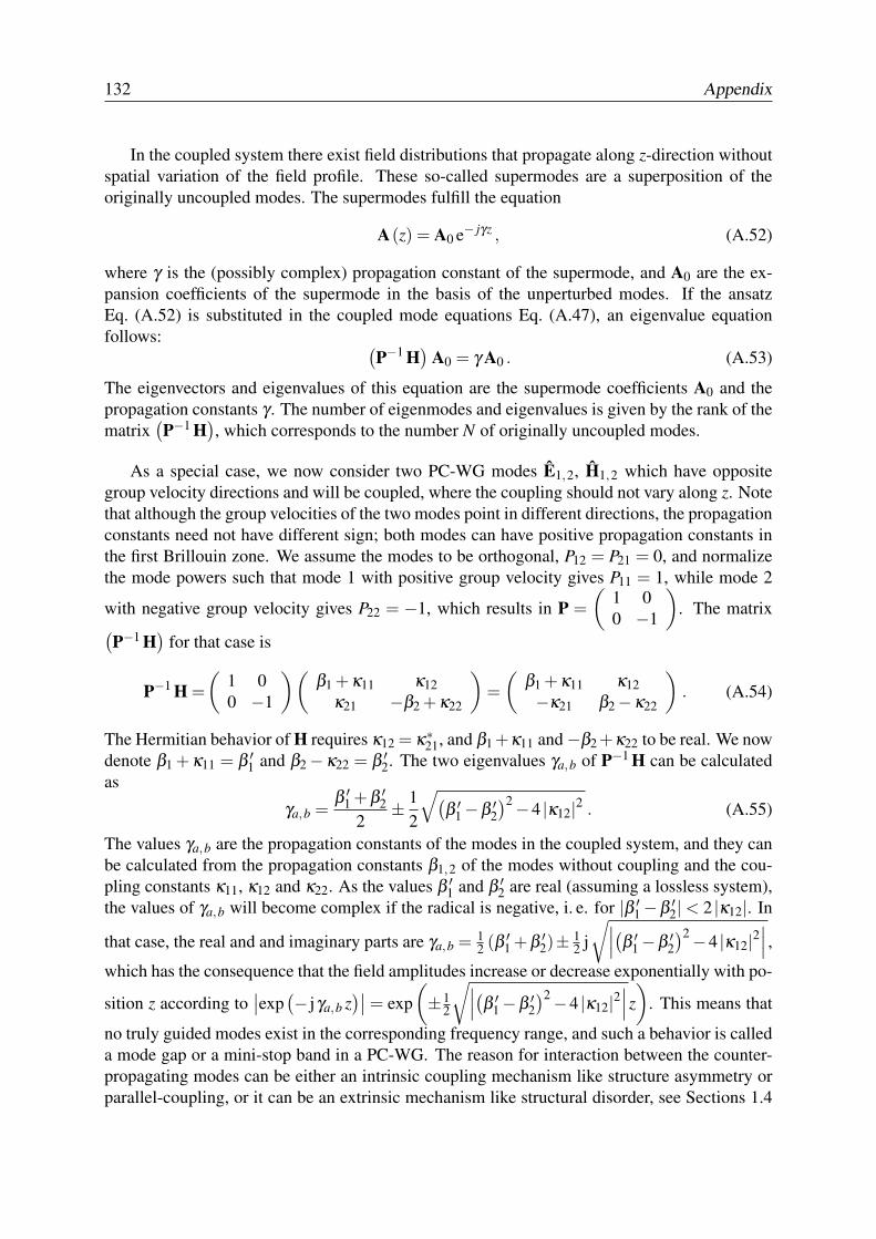
132 Appendix
In the coupled system there exist field distributions that propagate along z-direction withoutspatial variation of the field profile. These so-called supermodes are a superposition of theoriginally uncoupled modes. The supermodes fulfill the equation
A(z) = A0 e− jγz , (A.52)
where γ is the (possibly complex) propagation constant of the supermode, and A0 are the ex-pansion coefficients of the supermode in the basis of the unperturbed modes. If the ansatzEq. (A.52) is substituted in the coupled mode equations Eq. (A.47), an eigenvalue equationfollows: (
P−1 H)
A0 = γ A0 . (A.53)
The eigenvectors and eigenvalues of this equation are the supermode coefficients A0 and thepropagation constants γ . The number of eigenmodes and eigenvalues is given by the rank of thematrix
(P−1 H
), which corresponds to the number N of originally uncoupled modes.
As a special case, we now consider two PC-WG modes E1,2, H1,2 which have oppositegroup velocity directions and will be coupled, where the coupling should not vary along z. Notethat although the group velocities of the two modes point in different directions, the propagationconstants need not have different sign; both modes can have positive propagation constants inthe first Brillouin zone. We assume the modes to be orthogonal, P12 = P21 = 0, and normalizethe mode powers such that mode 1 with positive group velocity gives P11 = 1, while mode 2
with negative group velocity gives P22 = −1, which results in P =(
1 00 −1
). The matrix
(P−1 H
)for that case is
P−1 H =(
1 00 −1
)(β1 +κ11 κ12
κ21 −β2 +κ22
)=
(β1 +κ11 κ12−κ21 β2−κ22
). (A.54)
The Hermitian behavior of H requires κ12 = κ∗21, and β1 +κ11 and−β2 +κ22 to be real. We nowdenote β1 + κ11 = β ′1 and β2−κ22 = β ′2. The two eigenvalues γa,b of P−1 H can be calculatedas
γa,b =β ′1 +β ′2
2± 1
2
√(β ′1−β ′2
)2−4 |κ12|2 . (A.55)
The values γa,b are the propagation constants of the modes in the coupled system, and they canbe calculated from the propagation constants β1,2 of the modes without coupling and the cou-pling constants κ11, κ12 and κ22. As the values β ′1 and β ′2 are real (assuming a lossless system),the values of γa,b will become complex if the radical is negative, i. e. for |β ′1−β ′2|< 2 |κ12|. In
that case, the real and and imaginary parts are γa,b = 12 (β ′1 +β ′2)± 1
2 j√∣∣∣
(β ′1−β ′2
)2−4 |κ12|2∣∣∣ ,
which has the consequence that the field amplitudes increase or decrease exponentially with po-
sition z according to∣∣exp
(− jγa,b z)∣∣ = exp
(±1
2
√∣∣∣(β ′1−β ′2
)2−4 |κ12|2∣∣∣z
). This means that
no truly guided modes exist in the corresponding frequency range, and such a behavior is calleda mode gap or a mini-stop band in a PC-WG. The reason for interaction between the counter-propagating modes can be either an intrinsic coupling mechanism like structure asymmetry orparallel-coupling, or it can be an extrinsic mechanism like structural disorder, see Sections 1.4
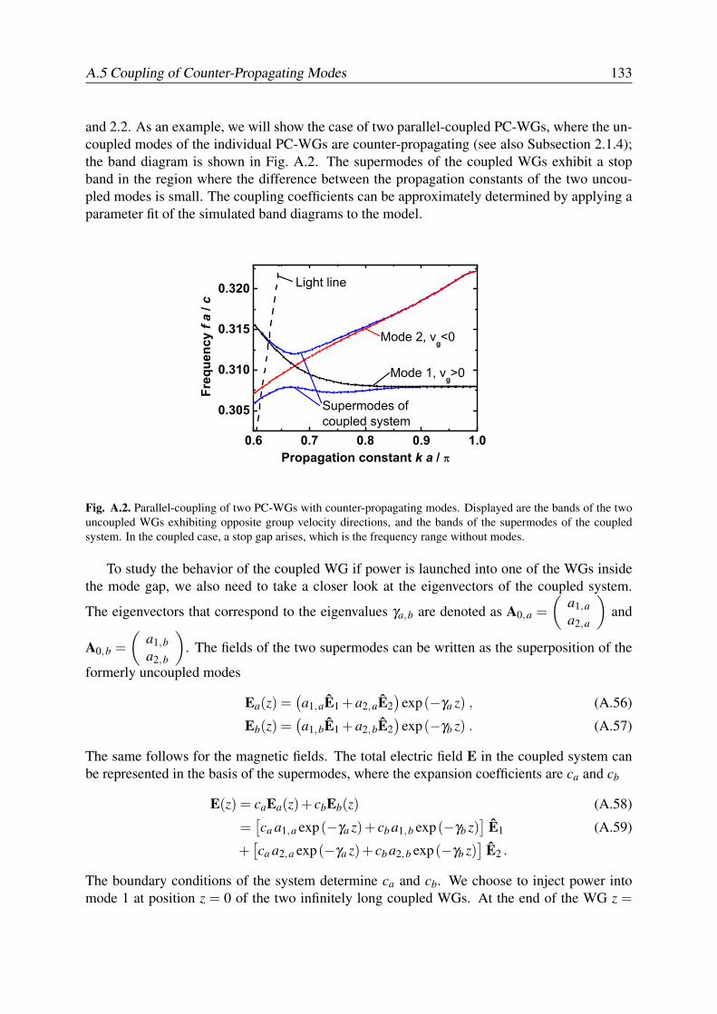
A.5 Coupling of Counter-Propagating Modes 133
and 2.2. As an example, we will show the case of two parallel-coupled PC-WGs, where the un-coupled modes of the individual PC-WGs are counter-propagating (see also Subsection 2.1.4);the band diagram is shown in Fig. A.2. The supermodes of the coupled WGs exhibit a stopband in the region where the difference between the propagation constants of the two uncou-pled modes is small. The coupling coefficients can be approximately determined by applying aparameter fit of the simulated band diagrams to the model.
0.6 0.7 0.8 0.9 1.0
0.305
0.310
0.315
0.320
Supermodes ofcoupled system
Mode 1, vg>0
Mode 2, vg<0
Light line
Freq
uenc
y f a
/ c
Propagation constant k a /
Fig. A.2. Parallel-coupling of two PC-WGs with counter-propagating modes. Displayed are the bands of the twouncoupled WGs exhibiting opposite group velocity directions, and the bands of the supermodes of the coupledsystem. In the coupled case, a stop gap arises, which is the frequency range without modes.
To study the behavior of the coupled WG if power is launched into one of the WGs insidethe mode gap, we also need to take a closer look at the eigenvectors of the coupled system.
The eigenvectors that correspond to the eigenvalues γa,b are denoted as A0,a =(
a1,aa2,a
)and
A0,b =(
a1,ba2,b
). The fields of the two supermodes can be written as the superposition of the
formerly uncoupled modes
Ea(z) =(a1,aE1 +a2,aE2
)exp(−γa z) , (A.56)
Eb(z) =(a1,bE1 +a2,bE2
)exp(−γb z) . (A.57)
The same follows for the magnetic fields. The total electric field E in the coupled system canbe represented in the basis of the supermodes, where the expansion coefficients are ca and cb
E(z) = caEa(z)+ cbEb(z) (A.58)
=[ca a1,a exp(−γa z)+ cb a1,b exp(−γb z)
]E1 (A.59)
+[ca a2,a exp(−γa z)+ cb a2,b exp(−γb z)
]E2 .
The boundary conditions of the system determine ca and cb. We choose to inject power intomode 1 at position z = 0 of the two infinitely long coupled WGs. At the end of the WG z =
134 Appendix
∞ no fields can exist, which requires the exponentially increasing function in Eq. (A.59) tovanish, which is only satisfied by choosing cb = 0. The field inside the WG is then given byE(z) = ca a1,a exp(−γa z) E1 + ca a2,a exp(−γa z) E2, which is the sum of the modes of the twooriginally uncoupled WGs with an exponential decay. The power injected in the first WG modeis transferred into the counter-propagating mode of the other WG, which means that all injectedpower will be reflected from the coupled WG system.
A.6 Loss Modeling 135
A.6 Loss ModelingHere, we sketch the solution of the differential equations that govern the power flow in a PC-WGwith backscattering αb and out-of-plane scattering αo (or the sum of out-of-plane and in-planescattering) as introduced in Subsection 2.2.1. Based on the coupled power equations [104], thedifferential equations to be solved are:
dPr(z)dz
=−(αb +αo)Pr +αbPl , (A.60)
dPl(z)dz
= (αb +αo)Pl−αbPr , (A.61)
where the total loss is αt = αb + αo. The boundary conditions that have to be met are that theinjected power at the beginning of the WG (position z = 0) is normalized to 1, Pr(0) = 1, and thereflected power at the end of the WG (position z = L) is zero, Pl(L) = 0. The Eqs. (A.60)-(A.61)can be solved by using the Laplace transform (s-transform), where a derivative is converted intoa multiplication with s and an additional summand that takes the boundary conditions at position0, Pr(0) and Pl(0), into account:
s pr (s)−Pr(0) =−αt pr (s)+αb pl (s) (A.62)s pl (s)−Pl(0) = αt pl (s)−αb pr (s) (A.63)
Equation (A.63) can be reshaped to pl (s) = Pl(0)−αb pr(s)s−αt
and substituted in Eq. (A.62) to isolatepr (s):
pr (s) =αb Pl(0)−αt Pr(0)
s2− (α2
t −α2b
) +sPr(0)
s2− (α2
t −α2b
) . (A.64)
The result is already separated into fractions that can be transformed back by using the corre-spondences sinh(αz) −• 1
s2−α2 , cosh(αz) −• ss2−α2 , α ∈ R, and the following result is ob-
tained:
Pr(z) =αbPl(0)−αtPr(0)√
α2t −α2
b
sinh(√
α2t −α2
b z)
+Pr(0)cosh(√
α2t −α2
b z)
. (A.65)
Substituting pr (s) from Eq. (A.64) into pl (s) = Pl(0)−αb pr(s)s−αt
leads to the solution for pl (s):
pl (s) =αt Pl(0)−αb Pr(0)
s2− (α2
t −α2b
) +sPl(0)
s2− (α2
t −α2b
) . (A.66)
Using the same correspondences as before, the result is
Pl(z) =αtPl(0)−αbPr(0)√
α2t −α2
b
sinh(√
α2t −α2
b z)
+Pl(0)cosh(√
α2t −α2
b z)
. (A.67)
From this equation, the conditions Pl(L) = 0 and Pr(0) = 1 allow solving for the backreflectionPl(0):
Pl(0) =αb tanh
(√α2
t −α2b L
)
αt tanh(√
α2t −α2
b L)
+√
α2t −α2
b
. (A.68)
136 Appendix
If the substitution α ≡√
α2t −α2
b is made, Eq. (A.68) results in Eq. (2.3). The transmittedpower Pr(L) is obtained from Eq. (A.65), where Pl(0) is known from Eq. (A.68):
Pr(L) =αb√
α2t −α2
b
sinh(√
α2t −α2
b L)
Pl(0)
+
cosh
(√α2
t −α2b L
)− αt√
α2t −α2
b
sinh(√
α2t −α2
b L)
. (A.69)
This again results in Eq. (2.4) with the substitution for α .
We also derive the solution of the simplified loss model:
dPr(z)dz
=−(αb +αo)Pr , (A.70)
dPl(z)dz
=−αbPr . (A.71)
The first equation, Eq. (A.70) can be directly integrated to yield
Pr (z) = Pr (0)e−αt L . (A.72)
This can be substituted into Eq. (A.70) and the solution can be found by integration:
dPl(z)dz
=−αbPr (0)e−αt L
⇒ Pl(z)−Pl(0) =αb
αtPr (0)
(e−αt z−1
)(A.73)
The boundary conditions Pl(L) = 0 and Pr(0) = 1 lead to the result for transmission and reflec-tion, Eqs. (2.8)-(2.9):
Pl(0) =αb
αt
(1− e−αtL
), (A.74)
Pr(L) = e−αtL . (A.75)
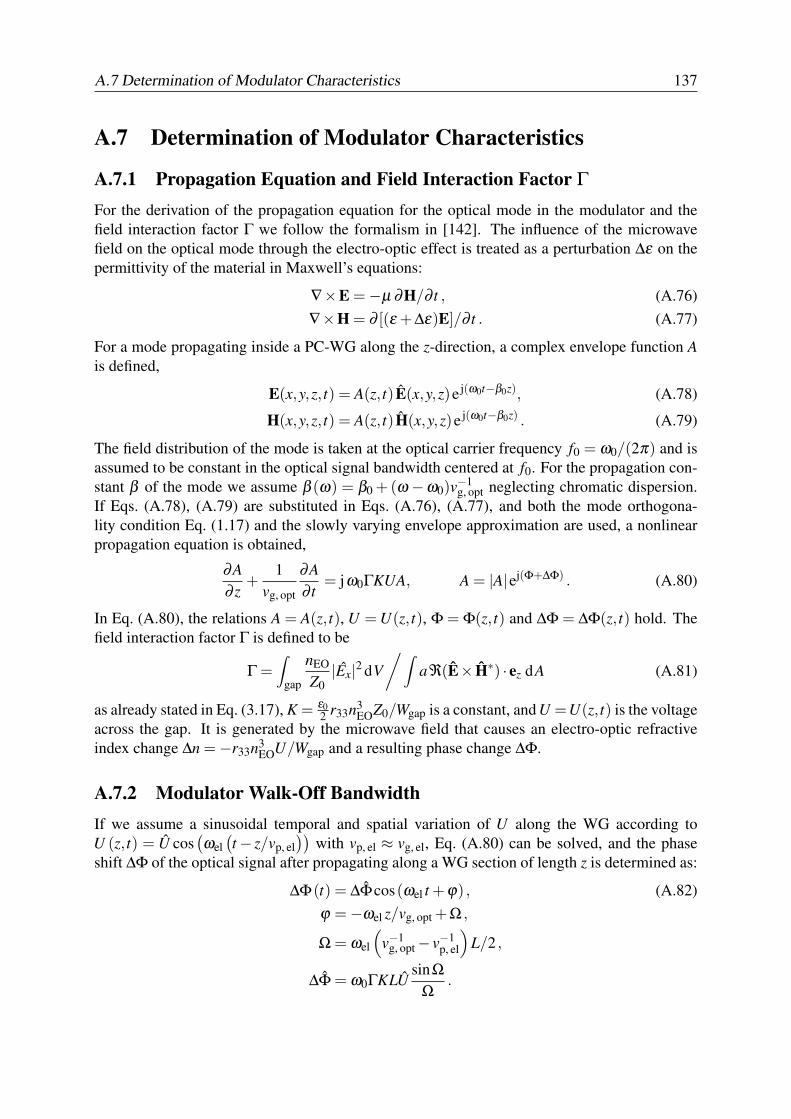
A.7 Determination of Modulator Characteristics 137
A.7 Determination of Modulator Characteristics
A.7.1 Propagation Equation and Field Interaction Factor ΓFor the derivation of the propagation equation for the optical mode in the modulator and thefield interaction factor Γ we follow the formalism in [142]. The influence of the microwavefield on the optical mode through the electro-optic effect is treated as a perturbation ∆ε on thepermittivity of the material in Maxwell’s equations:
∇×E =−µ ∂H/∂ t , (A.76)∇×H = ∂ [(ε +∆ε)E]/∂ t . (A.77)
For a mode propagating inside a PC-WG along the z-direction, a complex envelope function Ais defined,
E(x,y,z, t) = A(z, t) E(x,y,z)e j(ω0t−β0z), (A.78)
H(x,y,z, t) = A(z, t)H(x,y,z)e j(ω0t−β0z) . (A.79)
The field distribution of the mode is taken at the optical carrier frequency f0 = ω0/(2π) and isassumed to be constant in the optical signal bandwidth centered at f0. For the propagation con-stant β of the mode we assume β (ω) = β0 +(ω −ω0)v−1
g, opt neglecting chromatic dispersion.If Eqs. (A.78), (A.79) are substituted in Eqs. (A.76), (A.77), and both the mode orthogona-lity condition Eq. (1.17) and the slowly varying envelope approximation are used, a nonlinearpropagation equation is obtained,
∂A∂ z
+1
vg, opt
∂A∂ t
= jω0ΓKUA, A = |A|ej(Φ+∆Φ) . (A.80)
In Eq. (A.80), the relations A = A(z, t), U = U(z, t), Φ = Φ(z, t) and ∆Φ = ∆Φ(z, t) hold. Thefield interaction factor Γ is defined to be
Γ =∫
gap
nEO
Z0|Ex|2 dV
/∫aℜ(E× H∗) · ez dA (A.81)
as already stated in Eq. (3.17), K = ε02 r33n3
EOZ0/Wgap is a constant, and U =U(z, t) is the voltageacross the gap. It is generated by the microwave field that causes an electro-optic refractiveindex change ∆n =−r33n3
EOU/Wgap and a resulting phase change ∆Φ.
A.7.2 Modulator Walk-Off BandwidthIf we assume a sinusoidal temporal and spatial variation of U along the WG according toU (z, t) = U cos
(ωel
(t− z/vp, el
))with vp, el ≈ vg, el, Eq. (A.80) can be solved, and the phase
shift ∆Φ of the optical signal after propagating along a WG section of length z is determined as:
∆Φ(t) = ∆Φcos(ωel t +ϕ) , (A.82)ϕ =−ωel z/vg, opt +Ω ,
Ω = ωel
(v−1
g, opt− v−1p, el
)L/2 ,
∆Φ = ω0ΓKLUsinΩ
Ω.
138 Appendix
In the case of a DC electrical voltage where ωel = 0, U = U , and sinΩ/Ω = 1, this leads to aphase shift as also stated in Eq. (3.16):
∆Φ = ∆Φ = ω0ΓKLU for ωel = 0 (A.83)=−Γ∆nk0L .
For amplitude modulation at ωel 6= 0, two phase modulators are operated in a MZ push-pullconfiguration. The optical signals in both arms experience phase shifts of ∆Φ and −∆Φ, re-spectively. The arms are biased at ∆Φ0 = π/4, and an additional phase shift ∆Φ = π/4 isneeded to achieve complete extinction. The optical signal after the MZI is detected with aquadratic detector and generates an electrical current i:
i(t) ∝ cos2 (∆Φ0 +∆Φ(t)) = cos2 (∆Φ0 +∆Φcos(ωel t +ϕ)
). (A.84)
If the current spectrum I ( f ) is evaluated at the frequency fel = ωel/(2π), the dependence on∆Φ can be derived as I ( fel) ∝ J1
(2∆Φ( fel)
), where J1 is the Bessel-function of 1st order. The
3dB modulation bandwidth Eq. (3.13) is the frequency fel at which the magnitude of I ( fel) hasdecreased by a factor of 1/
√2 with respect to the DC case with ∆Φ( fel = 0) = π/4:
J1(2∆Φ( f3dB)
)= J1
(2∆Φ( fel = 0)
)/√
2 , (A.85)
Φ( f3dB)/Φ( fel = 0)≈ 0.564 .
According to Eq. (A.82), we find Φ( f3dB)/Φ( fel = 0) = sin(Ω( f3dB))/Ω( f3dB), which leadsto
Ω( f3dB)/π = fel
(v−1
g, opt− v−1p, el
)L≈ 0.556 , (A.86)
thus proving Eq. (3.13) with the accurate factor of 0.556. With an analogous calculation, thewalk-off bandwidth for counter-propagating electrical and optical signals can be determined,Eq. (3.14).
A.7.3 Modulator Bandwidth Limitations by RC-EffectsWe estimate the modulator bandwidth limitations that are caused by electrical RC-effects. Wediscuss two different mechanisms that reduce the electrical voltage drop across the gap andlead to an associated 3dB bandwidth. These are the generator-determined bandwidth and theparallel-loss determined bandwidth. We find that these bandwidth limitations do not play asignificant role for the presented structures.
For the following numerical examples, the data of our specific MZM design for a 78GHzmodulation bandwidth and a drive voltage of 1V were assumed, Fig. 3.12 and Fig. 3.13: Op-tical strip waveguide height h = 220nm, PM section length and gap width L = 80 µm andWgap = 150nm, linear refractive index of the PM section nEO = 1.6 (assumed to be the same atoptical and electrical frequencies), width of the doped silicon slabs w = 3 µm, vacuum dielectricconstant ε0, vacuum speed of light c.
1) Generator-Determined Bandwidth
The CPWG with wave impedance ZL = 50Ω be terminated with an open, Fig. A.3(a). Weassume the PM section to be short compared to the modulation signal wavelength, so that
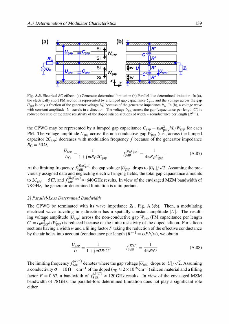
A.7 Determination of Modulator Characteristics 139
Fig. A.3. Electrical RC-effects. (a) Generator-determined limitation (b) Parallel-loss determined limitation. In (a),the electrically short PM section is represented by a lumped gap capacitance Cgap, and the voltage across the gapUgap is only a fraction of the generator voltage UG because of the generator impedance RG. In (b), a voltage wavewith constant amplitude |U | travels in z-direction. The voltage Ugap across the gap (capacitance per length C′) isreduced because of the finite resistivity of the doped silicon sections of width w (conductance per length (R ′−1).
the CPWG may be represented by a lumped gap capacitance Cgap = ε0n2polyhL/Wgap for each
PM. The voltage amplitude Ugap across the non-conductive gap Wgap (i. e., across the lumpedcapacitor 2Cgap) decreases with modulation frequency f because of the generator impedanceRG = 50Ω,
Ugap
UG=
11+ jωRG2Cgap
, f (RGCgap)3dB =
14πRGCgap
. (A.87)
At the limiting frequency f (RGCgap)3dB the gap voltage |Ugap| drops to |UG|/
√2. Assuming the pre-
viously assigned data and neglecting electric fringing fields, the total gap capacitance amountsto 2Cgap = 5fF, and f (RGCgap)
3dB ≈ 640GHz results. In view of the envisaged MZM bandwidth of78GHz, the generator-determined limitation is unimportant.
2) Parallel-Loss Determined Bandwidth
The CPWG be terminated with its wave impedance ZL, Fig. A.3(b). Then, a modulatingelectrical wave traveling in z-direction has a spatially constant amplitude |U |. The result-ing voltage amplitude |Ugap| across the non-conductive gap Wgap (PM capacitance per lengthC′ = ε0n2
EOh/Wgap) is reduced because of the finite resistivity of the doped silicon. For siliconsections having a width w and a filling factor F taking the reduction of the effective conductanceby the air holes into account (conductance per length (R ′−1 = σFh/w), we obtain
Ugap
U=
11+ jω2R ′C′
, f (R ′C′)3dB =
14πR ′C′
(A.88)
The limiting frequency f (R ′C′)3dB denotes where the gap voltage |Ugap| drops to |U |/√2. Assuming
a conductivity σ = 10Ω−1 cm−1 of the doped (nD ≈ 2×1016 cm−3) silicon material and a fillingfactor F = 0.67, a bandwidth of f (R ′C′)
3dB ≈ 120GHz results. In view of the envisaged MZMbandwidth of 78GHz, the parallel-loss determined limitation does not play a significant roleeither.
140 Appendix
3) Other Effects
Basically, one might think of a bandwidth limitation by the finite carrier transit time in the dopedsilicon slabs, see Fig. 3.13. This carrier drift time is determined by the slower carriers, whichin silicon are holes, the maximum saturation velocity of which is about 0.6× 107 cm/s. Overthe 3 µm witdh of the silicon slab, this would lead to a response time in the order of τD = 50ps,resulting in a bandwidth in the order of 3GHz only.
However, there is also the dielectric dielectric relaxation time τR, inside which any chargeperturbation in the doped silicon slabs (induced by the modulating field) is screened by a shiftof the whole carrier ensemble. The dielectric relaxation time τR = ε0 εr/σ depends on thematerial’s conductivity σ and permittivity ε0 εr. For σ = 10Ω−1 cm−1 as assumed above andwith εr = 12, a value of τR = 0.1ps is obtained.
For the resulting response time τ−1res = τ−1
D + τ−1R ≈ τ−1
R , the faster of the two effects isrelevant, and the bandwidth limited by the dielectric relaxation time would be 1.6THz. As aconsequence, carrier transit times do not limit the modulator’s performance.
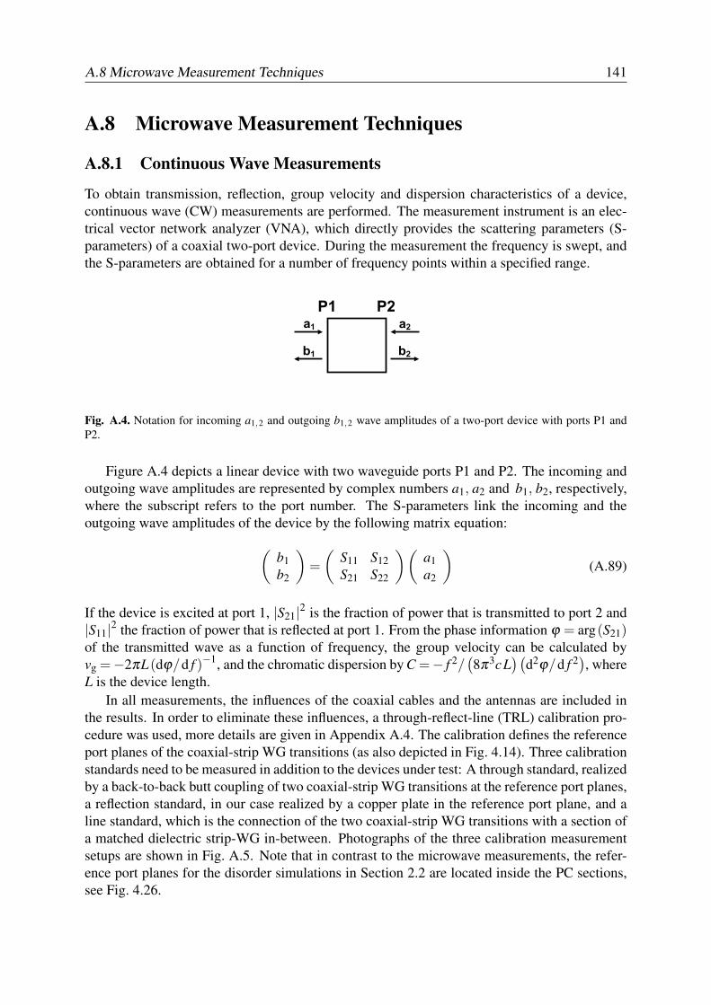
A.8 Microwave Measurement Techniques 141
A.8 Microwave Measurement Techniques
A.8.1 Continuous Wave Measurements
To obtain transmission, reflection, group velocity and dispersion characteristics of a device,continuous wave (CW) measurements are performed. The measurement instrument is an elec-trical vector network analyzer (VNA), which directly provides the scattering parameters (S-parameters) of a coaxial two-port device. During the measurement the frequency is swept, andthe S-parameters are obtained for a number of frequency points within a specified range.
Fig. A.4. Notation for incoming a1,2 and outgoing b1,2 wave amplitudes of a two-port device with ports P1 andP2.
Figure A.4 depicts a linear device with two waveguide ports P1 and P2. The incoming andoutgoing wave amplitudes are represented by complex numbers a1, a2 and b1, b2, respectively,where the subscript refers to the port number. The S-parameters link the incoming and theoutgoing wave amplitudes of the device by the following matrix equation:
(b1b2
)=
(S11 S12S21 S22
)(a1a2
)(A.89)
If the device is excited at port 1, |S21|2 is the fraction of power that is transmitted to port 2 and|S11|2 the fraction of power that is reflected at port 1. From the phase information ϕ = arg(S21)of the transmitted wave as a function of frequency, the group velocity can be calculated byvg =−2πL(dϕ/d f )−1, and the chromatic dispersion by C =− f 2/
(8π3cL
)(d2ϕ/d f 2), where
L is the device length.In all measurements, the influences of the coaxial cables and the antennas are included in
the results. In order to eliminate these influences, a through-reflect-line (TRL) calibration pro-cedure was used, more details are given in Appendix A.4. The calibration defines the referenceport planes of the coaxial-strip WG transitions (as also depicted in Fig. 4.14). Three calibrationstandards need to be measured in addition to the devices under test: A through standard, realizedby a back-to-back butt coupling of two coaxial-strip WG transitions at the reference port planes,a reflection standard, in our case realized by a copper plate in the reference port plane, and aline standard, which is the connection of the two coaxial-strip WG transitions with a section ofa matched dielectric strip-WG in-between. Photographs of the three calibration measurementsetups are shown in Fig. A.5. Note that in contrast to the microwave measurements, the refer-ence port planes for the disorder simulations in Section 2.2 are located inside the PC sections,see Fig. 4.26.
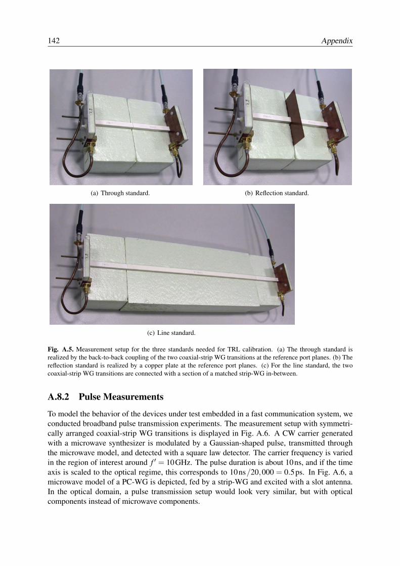
142 Appendix
(a) Through standard. (b) Reflection standard.
(c) Line standard.
Fig. A.5. Measurement setup for the three standards needed for TRL calibration. (a) The through standard isrealized by the back-to-back coupling of the two coaxial-strip WG transitions at the reference port planes. (b) Thereflection standard is realized by a copper plate at the reference port planes. (c) For the line standard, the twocoaxial-strip WG transitions are connected with a section of a matched strip-WG in-between.
A.8.2 Pulse Measurements
To model the behavior of the devices under test embedded in a fast communication system, weconducted broadband pulse transmission experiments. The measurement setup with symmetri-cally arranged coaxial-strip WG transitions is displayed in Fig. A.6. A CW carrier generatedwith a microwave synthesizer is modulated by a Gaussian-shaped pulse, transmitted throughthe microwave model, and detected with a square law detector. The carrier frequency is variedin the region of interest around f ′ = 10GHz. The pulse duration is about 10ns, and if the timeaxis is scaled to the optical regime, this corresponds to 10ns/20,000 = 0.5ps. In Fig. A.6, amicrowave model of a PC-WG is depicted, fed by a strip-WG and excited with a slot antenna.In the optical domain, a pulse transmission setup would look very similar, but with opticalcomponents instead of microwave components.
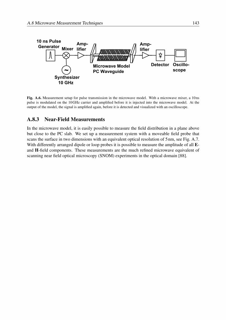
A.8 Microwave Measurement Techniques 143
Fig. A.6. Measurement setup for pulse transmission in the microwave model. With a microwave mixer, a 10nspulse is modulated on the 10GHz carrier and amplified before it is injected into the microwave model. At theoutput of the model, the signal is amplified again, before it is detected and visualized with an oscilloscope.
A.8.3 Near-Field MeasurementsIn the microwave model, it is easily possible to measure the field distribution in a plane abovebut close to the PC slab. We set up a measurement system with a moveable field probe thatscans the surface in two dimensions with an equivalent optical resolution of 5nm, see Fig. A.7.With differently arranged dipole or loop probes it is possible to measure the amplitude of all E-and H-field components. These measurements are the much refined microwave equivalent ofscanning near field optical microscopy (SNOM) experiments in the optical domain [88].
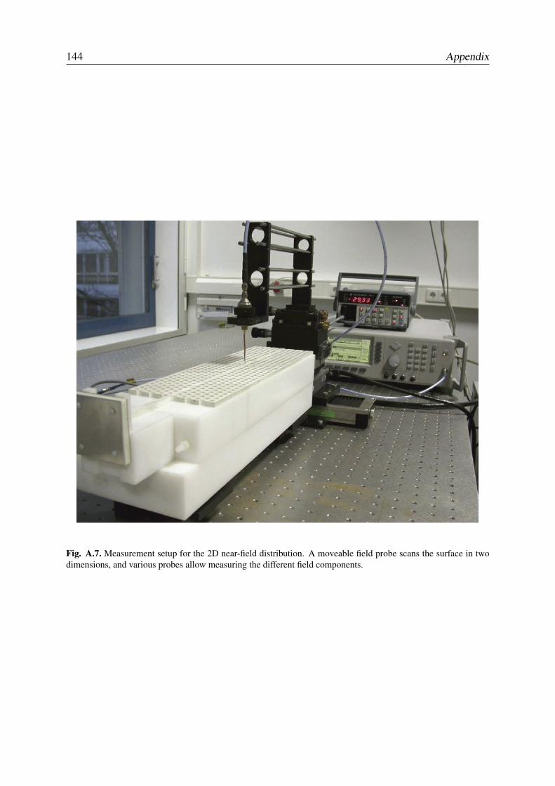
144 Appendix
Fig. A.7. Measurement setup for the 2D near-field distribution. A moveable field probe scans the surface in twodimensions, and various probes allow measuring the different field components.
Glossary
Acronyms2D Two-dimensional3D Three-dimensionalCMOS Complementary metal oxide semiconductorCPO Coherent population oscillationCPWG Coplanar waveguideCROW Coupled-resonator optical waveguideCW Continuous waveDCF Dispersion compensating fiberDUT Device under testEIT Electromagnetically induced transparencyFCA Free-carrier absorptionFDTD Finite difference time domainFIT Finite integration techniqueFWHM Full width at half maximumGME Guided mode expansionMZ Mach-ZehnderMZI Mach-Zehnder interferometerMZM Mach-Zehnder modulatorPBG Photonic bandgapPC Photonic crystalPM Phase modulatorPWE Plane wave expansionRMS Root mean squareSBS Stimulated Brillouin scatteringSEM Scanning electron microscopeSMF Single mode fiberSOI Silicon-on-insulatorSRS Stimulated Raman scatteringTE Transverse electric
145

146 Glossary
TIR Total internal reflectionTM Transverse magneticTPA Two-photon absorptionTRL Thru-reflect-lineWG Waveguide
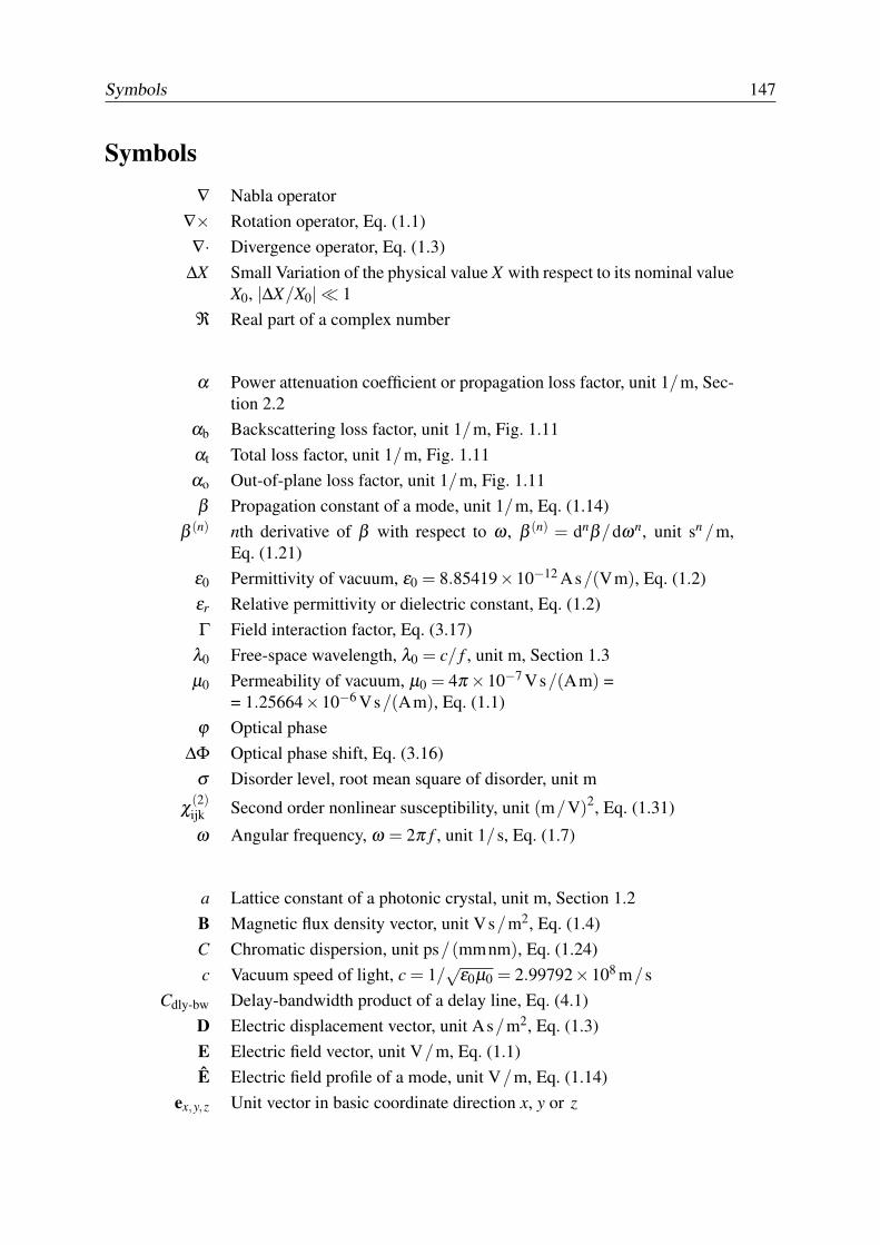
Symbols 147
Symbols∇ Nabla operator
∇× Rotation operator, Eq. (1.1)∇· Divergence operator, Eq. (1.3)
∆X Small Variation of the physical value X with respect to its nominal valueX0, |∆X/X0| ¿ 1
ℜ Real part of a complex number
α Power attenuation coefficient or propagation loss factor, unit 1/m, Sec-tion 2.2
αb Backscattering loss factor, unit 1/m, Fig. 1.11αt Total loss factor, unit 1/m, Fig. 1.11αo Out-of-plane loss factor, unit 1/m, Fig. 1.11β Propagation constant of a mode, unit 1/m, Eq. (1.14)
β (n) nth derivative of β with respect to ω , β (n) = dnβ/dωn, unit sn /m,Eq. (1.21)
ε0 Permittivity of vacuum, ε0 = 8.85419×10⁻¹² As/(Vm), Eq. (1.2)εr Relative permittivity or dielectric constant, Eq. (1.2)Γ Field interaction factor, Eq. (3.17)
λ0 Free-space wavelength, λ0 = c/ f , unit m, Section 1.3µ0 Permeability of vacuum, µ0 = 4π×10−7 Vs/(Am) =
= 1.25664×10⁻⁶ Vs/(Am), Eq. (1.1)ϕ Optical phase
∆Φ Optical phase shift, Eq. (3.16)σ Disorder level, root mean square of disorder, unit m
χ(2)ijk Second order nonlinear susceptibility, unit (m/V)2, Eq. (1.31)
ω Angular frequency, ω = 2π f , unit 1/s, Eq. (1.7)
a Lattice constant of a photonic crystal, unit m, Section 1.2B Magnetic flux density vector, unit Vs/m2, Eq. (1.4)C Chromatic dispersion, unit ps/(mmnm), Eq. (1.24)c Vacuum speed of light, c = 1/
√ε0µ0 = 2.99792×10⁸ m/sCdly-bw Delay-bandwidth product of a delay line, Eq. (4.1)
D Electric displacement vector, unit As/m2, Eq. (1.3)E Electric field vector, unit V/m, Eq. (1.1)E Electric field profile of a mode, unit V/m, Eq. (1.14)
ex,y,z Unit vector in basic coordinate direction x, y or z
148 Glossary
f Frequency, unit Hzf3dB 3dB modulation bandwidth, unit Hz, Eq. (3.12)∆ f Bandwidth, unit HzG Reciprocal lattice vectors of a photonic crystal, unit 1/m, Section 1.2H Magnetic field vector, unit A/m, Eq. (1.1)H Magnetic field profile of a mode, unit A/m, Eq. (1.15)h Slab height of a structure, unit mj Imaginary unit, j2 =−1
k Wave vector, unit 1/m, Eq. (1.19)k Propagation constant, unit 1/m, Eq. (1.20)
L, l Length of a structure, unit mn Refractive index, n = ε2
r
neff Effective refractive index, Eq. 1.16ng Group index, Section (1.3)P Power of a mode, unit W, Eq. (1.18)R Lattice vectors of a photonic crystal, unit m, Section 1.2r Spatial coordinate vector, r = (x,y,z), unit mr Radius of a photonic crystal hole, unit m
rij Electro-optic coefficient, unit m/V, Eq. (1.34)Sij Scattering parameters of a device, Eq. (A.24)
t Time, unit stg Group delay, tg = L/vg, unit s, Section 1.3U Voltage, unit V
Uπ Required modulation voltage to generate a π phase shift, unit V,Eq. (3.12)
U Amplitude of modulation voltage, unit V, Section 3.3.4u Periodic part of a photonic crystal mode, Eq. (1.19)
vp Phase velocity, unit m/s, Eq. (1.22)vg Group velocity, unit m/s, Eq. (1.23)W Geometrical width, unit m
x, y, z Spatial coordinates, unit m, Fig. 1.1Z0 Wave impedance of free space, Z0 =
√µ0/ε0 = 376.73Ω, Eq. (3.17)
Bibliography
[1] J. M. Brosi, C. Koos, L. C. Andreani, M. Waldow, J. Leuthold, and W. Freude, “High-speed low-voltage electro-optic modulator with a polymer-infiltrated silicon photoniccrystal waveguide,” Opt. Express, vol. 16, pp. 4177–4191, 2008.
[2] J. M. Brosi, J. Leuthold, and W. Freude, “Microwave-frequency experiments validate op-tical simulation tools and demonstrate novel dispersion-tailored photonic crystal wave-guides,” J. Lightw. Technol., vol. 25, pp. 2502–2510, 2007.
[3] E. Yablonovitch, “Inhibited spontaneous emission in solid-state physics and electronics,”Phys. Rev. Lett., vol. 58, pp. 2059–2062, 1987.
[4] S. John, “Strong localization of photons in certain disordered dielectric superlattices,”Phys. Rev. Lett., vol. 58, pp. 2486–2489, 1987.
[5] E. Yablonovitch and T. J. Gmitter, “Photonic band structure: The face-centered-cubiccase,” Phys. Rev. Lett., vol. 63, pp. 1950–1953, 1989.
[6] E. Yablonovitch and T. J. Gmitter, “Donor and acceptor modes in photonic band struc-tures,” Phys. Rev. Lett., vol. 67, pp. 3380–3383, 1991.
[7] J. D. Jackson, Classical Electrodynamics. New York: John Wiley and Sons, 1998.
[8] J. A. Kong, Electromagnetic Wave Theory. Cambridge, Massachusetts: EMW Publish-ing, 2000.
[9] J. D. Joannopoulos, R. D. Meade, and J. N. Winn, Photonic Crystals: Molding the Flowof Light. New Jersey: Princeton University Press, 1995.
[10] D. Marcuse, Light Transmission Optics. New York: Van Nostrand Reinhold, 1972.
[11] S. G. Johnson, S. Fan, P. R. Villeneuve, J. D. Joannopoulos, and L. A. Kolodziejski,“Guided modes in photonic crystal slabs,” Phys. Rev. E, vol. 60, pp. 5751–5758, 1999.
[12] M. Loncar, D. Nedeljkovic, T. Doll, J. Vuckovic, A. Scherer, and T. P. Pearsall, “Wave-guiding in planar photonic crystals,” Appl. Phys. Lett., vol. 77, pp. 1937–1939, 2000.
[13] S. G. Johnson, P. R. Villeneuve, S. Fan, and J. D. Joannopoulos, “Linear waveguides inphotonic-crystal slabs,” Phys. Rev. B, vol. 62, pp. 8212–8222, 2000.
149
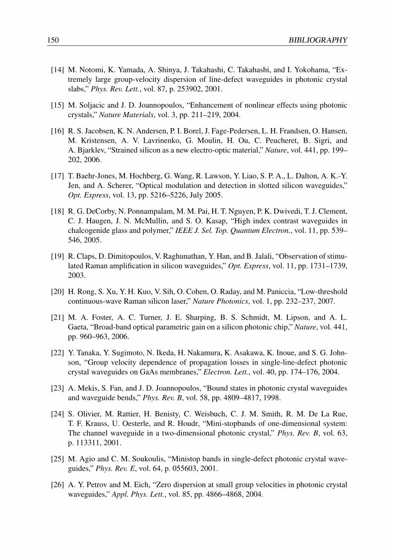
150 BIBLIOGRAPHY
[14] M. Notomi, K. Yamada, A. Shinya, J. Takahashi, C. Takahashi, and I. Yokohama, “Ex-tremely large group-velocity dispersion of line-defect waveguides in photonic crystalslabs,” Phys. Rev. Lett., vol. 87, p. 253902, 2001.
[15] M. Soljacic and J. D. Joannopoulos, “Enhancement of nonlinear effects using photoniccrystals,” Nature Materials, vol. 3, pp. 211–219, 2004.
[16] R. S. Jacobsen, K. N. Andersen, P. I. Borel, J. Fage-Pedersen, L. H. Frandsen, O. Hansen,M. Kristensen, A. V. Lavrinenko, G. Moulin, H. Ou, C. Peucheret, B. Sigri, andA. Bjarklev, “Strained silicon as a new electro-optic material,” Nature, vol. 441, pp. 199–202, 2006.
[17] T. Baehr-Jones, M. Hochberg, G. Wang, R. Lawson, Y. Liao, S. P. A., L. Dalton, A. K.-Y.Jen, and A. Scherer, “Optical modulation and detection in slotted silicon waveguides,”Opt. Express, vol. 13, pp. 5216–5226, July 2005.
[18] R. G. DeCorby, N. Ponnampalam, M. M. Pai, H. T. Nguyen, P. K. Dwivedi, T. J. Clement,C. J. Haugen, J. N. McMullin, and S. O. Kasap, “High index contrast waveguides inchalcogenide glass and polymer,” IEEE J. Sel. Top. Quantum Electron., vol. 11, pp. 539–546, 2005.
[19] R. Claps, D. Dimitopoulos, V. Raghunathan, Y. Han, and B. Jalali, “Observation of stimu-lated Raman amplification in silicon waveguides,” Opt. Express, vol. 11, pp. 1731–1739,2003.
[20] H. Rong, S. Xu, Y. H. Kuo, V. Sih, O. Cohen, O. Raday, and M. Paniccia, “Low-thresholdcontinuous-wave Raman silicon laser,” Nature Photonics, vol. 1, pp. 232–237, 2007.
[21] M. A. Foster, A. C. Turner, J. E. Sharping, B. S. Schmidt, M. Lipson, and A. L.Gaeta, “Broad-band optical parametric gain on a silicon photonic chip,” Nature, vol. 441,pp. 960–963, 2006.
[22] Y. Tanaka, Y. Sugimoto, N. Ikeda, H. Nakamura, K. Asakawa, K. Inoue, and S. G. John-son, “Group velocity dependence of propagation losses in single-line-defect photoniccrystal waveguides on GaAs membranes,” Electron. Lett., vol. 40, pp. 174–176, 2004.
[23] A. Mekis, S. Fan, and J. D. Joannopoulos, “Bound states in photonic crystal waveguidesand waveguide bends,” Phys. Rev. B, vol. 58, pp. 4809–4817, 1998.
[24] S. Olivier, M. Rattier, H. Benisty, C. Weisbuch, C. J. M. Smith, R. M. De La Rue,T. F. Krauss, U. Oesterle, and R. Houdr, “Mini-stopbands of one-dimensional system:The channel waveguide in a two-dimensional photonic crystal,” Phys. Rev. B, vol. 63,p. 113311, 2001.
[25] M. Agio and C. M. Soukoulis, “Ministop bands in single-defect photonic crystal wave-guides,” Phys. Rev. E, vol. 64, p. 055603, 2001.
[26] A. Y. Petrov and M. Eich, “Zero dispersion at small group velocities in photonic crystalwaveguides,” Appl. Phys. Lett., vol. 85, pp. 4866–4868, 2004.
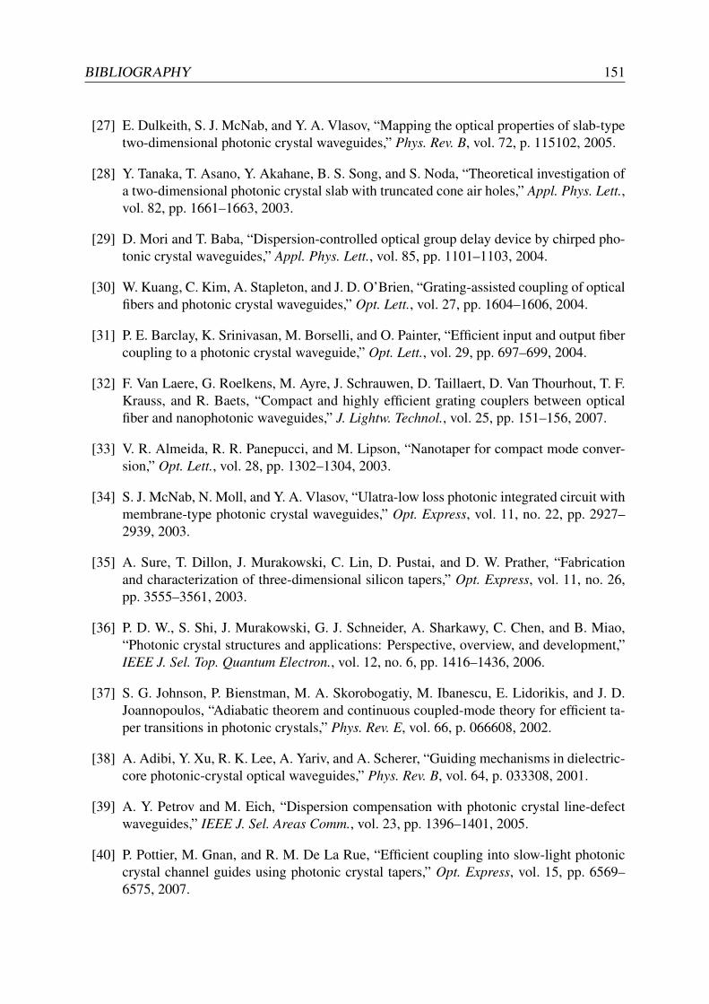
BIBLIOGRAPHY 151
[27] E. Dulkeith, S. J. McNab, and Y. A. Vlasov, “Mapping the optical properties of slab-typetwo-dimensional photonic crystal waveguides,” Phys. Rev. B, vol. 72, p. 115102, 2005.
[28] Y. Tanaka, T. Asano, Y. Akahane, B. S. Song, and S. Noda, “Theoretical investigation ofa two-dimensional photonic crystal slab with truncated cone air holes,” Appl. Phys. Lett.,vol. 82, pp. 1661–1663, 2003.
[29] D. Mori and T. Baba, “Dispersion-controlled optical group delay device by chirped pho-tonic crystal waveguides,” Appl. Phys. Lett., vol. 85, pp. 1101–1103, 2004.
[30] W. Kuang, C. Kim, A. Stapleton, and J. D. O’Brien, “Grating-assisted coupling of opticalfibers and photonic crystal waveguides,” Opt. Lett., vol. 27, pp. 1604–1606, 2004.
[31] P. E. Barclay, K. Srinivasan, M. Borselli, and O. Painter, “Efficient input and output fibercoupling to a photonic crystal waveguide,” Opt. Lett., vol. 29, pp. 697–699, 2004.
[32] F. Van Laere, G. Roelkens, M. Ayre, J. Schrauwen, D. Taillaert, D. Van Thourhout, T. F.Krauss, and R. Baets, “Compact and highly efficient grating couplers between opticalfiber and nanophotonic waveguides,” J. Lightw. Technol., vol. 25, pp. 151–156, 2007.
[33] V. R. Almeida, R. R. Panepucci, and M. Lipson, “Nanotaper for compact mode conver-sion,” Opt. Lett., vol. 28, pp. 1302–1304, 2003.
[34] S. J. McNab, N. Moll, and Y. A. Vlasov, “Ulatra-low loss photonic integrated circuit withmembrane-type photonic crystal waveguides,” Opt. Express, vol. 11, no. 22, pp. 2927–2939, 2003.
[35] A. Sure, T. Dillon, J. Murakowski, C. Lin, D. Pustai, and D. W. Prather, “Fabricationand characterization of three-dimensional silicon tapers,” Opt. Express, vol. 11, no. 26,pp. 3555–3561, 2003.
[36] P. D. W., S. Shi, J. Murakowski, G. J. Schneider, A. Sharkawy, C. Chen, and B. Miao,“Photonic crystal structures and applications: Perspective, overview, and development,”IEEE J. Sel. Top. Quantum Electron., vol. 12, no. 6, pp. 1416–1436, 2006.
[37] S. G. Johnson, P. Bienstman, M. A. Skorobogatiy, M. Ibanescu, E. Lidorikis, and J. D.Joannopoulos, “Adiabatic theorem and continuous coupled-mode theory for efficient ta-per transitions in photonic crystals,” Phys. Rev. E, vol. 66, p. 066608, 2002.
[38] A. Adibi, Y. Xu, R. K. Lee, A. Yariv, and A. Scherer, “Guiding mechanisms in dielectric-core photonic-crystal optical waveguides,” Phys. Rev. B, vol. 64, p. 033308, 2001.
[39] A. Y. Petrov and M. Eich, “Dispersion compensation with photonic crystal line-defectwaveguides,” IEEE J. Sel. Areas Comm., vol. 23, pp. 1396–1401, 2005.
[40] P. Pottier, M. Gnan, and R. M. De La Rue, “Efficient coupling into slow-light photoniccrystal channel guides using photonic crystal tapers,” Opt. Express, vol. 15, pp. 6569–6575, 2007.
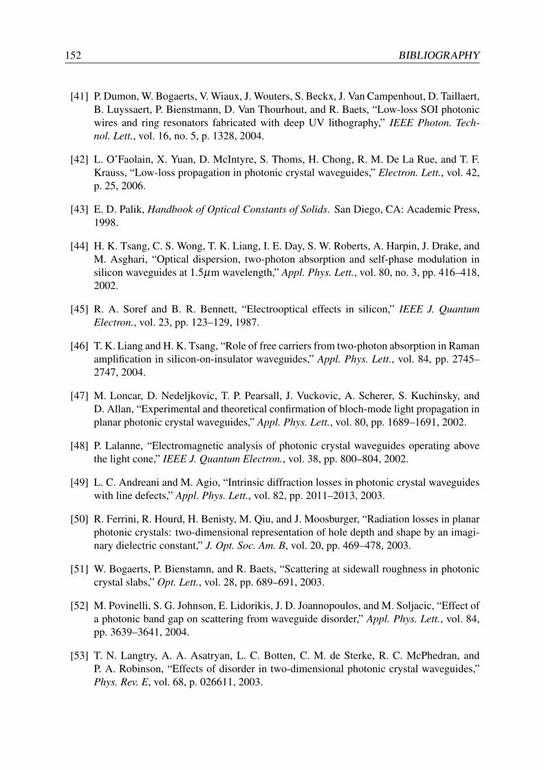
152 BIBLIOGRAPHY
[41] P. Dumon, W. Bogaerts, V. Wiaux, J. Wouters, S. Beckx, J. Van Campenhout, D. Taillaert,B. Luyssaert, P. Bienstmann, D. Van Thourhout, and R. Baets, “Low-loss SOI photonicwires and ring resonators fabricated with deep UV lithography,” IEEE Photon. Tech-nol. Lett., vol. 16, no. 5, p. 1328, 2004.
[42] L. O’Faolain, X. Yuan, D. McIntyre, S. Thoms, H. Chong, R. M. De La Rue, and T. F.Krauss, “Low-loss propagation in photonic crystal waveguides,” Electron. Lett., vol. 42,p. 25, 2006.
[43] E. D. Palik, Handbook of Optical Constants of Solids. San Diego, CA: Academic Press,1998.
[44] H. K. Tsang, C. S. Wong, T. K. Liang, I. E. Day, S. W. Roberts, A. Harpin, J. Drake, andM. Asghari, “Optical dispersion, two-photon absorption and self-phase modulation insilicon waveguides at 1.5µm wavelength,” Appl. Phys. Lett., vol. 80, no. 3, pp. 416–418,2002.
[45] R. A. Soref and B. R. Bennett, “Electrooptical effects in silicon,” IEEE J. QuantumElectron., vol. 23, pp. 123–129, 1987.
[46] T. K. Liang and H. K. Tsang, “Role of free carriers from two-photon absorption in Ramanamplification in silicon-on-insulator waveguides,” Appl. Phys. Lett., vol. 84, pp. 2745–2747, 2004.
[47] M. Loncar, D. Nedeljkovic, T. P. Pearsall, J. Vuckovic, A. Scherer, S. Kuchinsky, andD. Allan, “Experimental and theoretical confirmation of bloch-mode light propagation inplanar photonic crystal waveguides,” Appl. Phys. Lett., vol. 80, pp. 1689–1691, 2002.
[48] P. Lalanne, “Electromagnetic analysis of photonic crystal waveguides operating abovethe light cone,” IEEE J. Quantum Electron., vol. 38, pp. 800–804, 2002.
[49] L. C. Andreani and M. Agio, “Intrinsic diffraction losses in photonic crystal waveguideswith line defects,” Appl. Phys. Lett., vol. 82, pp. 2011–2013, 2003.
[50] R. Ferrini, R. Hourd, H. Benisty, M. Qiu, and J. Moosburger, “Radiation losses in planarphotonic crystals: two-dimensional representation of hole depth and shape by an imagi-nary dielectric constant,” J. Opt. Soc. Am. B, vol. 20, pp. 469–478, 2003.
[51] W. Bogaerts, P. Bienstamn, and R. Baets, “Scattering at sidewall roughness in photoniccrystal slabs,” Opt. Lett., vol. 28, pp. 689–691, 2003.
[52] M. Povinelli, S. G. Johnson, E. Lidorikis, J. D. Joannopoulos, and M. Soljacic, “Effect ofa photonic band gap on scattering from waveguide disorder,” Appl. Phys. Lett., vol. 84,pp. 3639–3641, 2004.
[53] T. N. Langtry, A. A. Asatryan, L. C. Botten, C. M. de Sterke, R. C. McPhedran, andP. A. Robinson, “Effects of disorder in two-dimensional photonic crystal waveguides,”Phys. Rev. E, vol. 68, p. 026611, 2003.
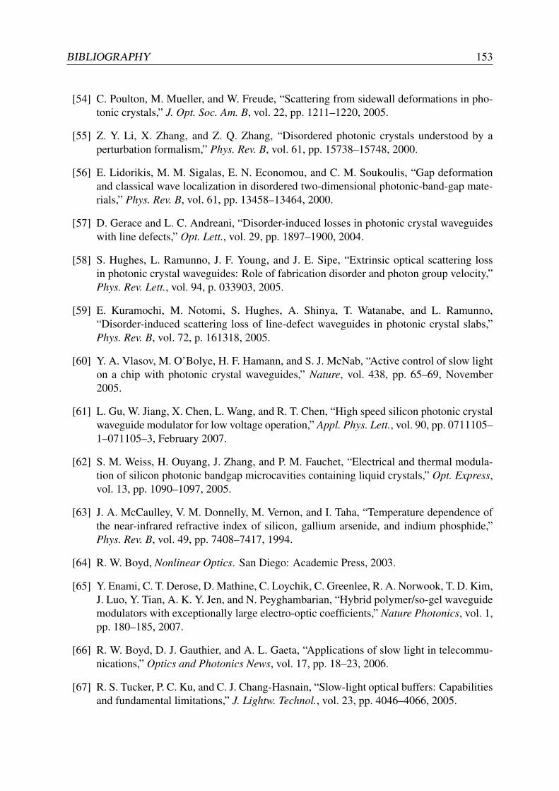
BIBLIOGRAPHY 153
[54] C. Poulton, M. Mueller, and W. Freude, “Scattering from sidewall deformations in pho-tonic crystals,” J. Opt. Soc. Am. B, vol. 22, pp. 1211–1220, 2005.
[55] Z. Y. Li, X. Zhang, and Z. Q. Zhang, “Disordered photonic crystals understood by aperturbation formalism,” Phys. Rev. B, vol. 61, pp. 15738–15748, 2000.
[56] E. Lidorikis, M. M. Sigalas, E. N. Economou, and C. M. Soukoulis, “Gap deformationand classical wave localization in disordered two-dimensional photonic-band-gap mate-rials,” Phys. Rev. B, vol. 61, pp. 13458–13464, 2000.
[57] D. Gerace and L. C. Andreani, “Disorder-induced losses in photonic crystal waveguideswith line defects,” Opt. Lett., vol. 29, pp. 1897–1900, 2004.
[58] S. Hughes, L. Ramunno, J. F. Young, and J. E. Sipe, “Extrinsic optical scattering lossin photonic crystal waveguides: Role of fabrication disorder and photon group velocity,”Phys. Rev. Lett., vol. 94, p. 033903, 2005.
[59] E. Kuramochi, M. Notomi, S. Hughes, A. Shinya, T. Watanabe, and L. Ramunno,“Disorder-induced scattering loss of line-defect waveguides in photonic crystal slabs,”Phys. Rev. B, vol. 72, p. 161318, 2005.
[60] Y. A. Vlasov, M. O’Bolye, H. F. Hamann, and S. J. McNab, “Active control of slow lighton a chip with photonic crystal waveguides,” Nature, vol. 438, pp. 65–69, November2005.
[61] L. Gu, W. Jiang, X. Chen, L. Wang, and R. T. Chen, “High speed silicon photonic crystalwaveguide modulator for low voltage operation,” Appl. Phys. Lett., vol. 90, pp. 0711105–1–071105–3, February 2007.
[62] S. M. Weiss, H. Ouyang, J. Zhang, and P. M. Fauchet, “Electrical and thermal modula-tion of silicon photonic bandgap microcavities containing liquid crystals,” Opt. Express,vol. 13, pp. 1090–1097, 2005.
[63] J. A. McCaulley, V. M. Donnelly, M. Vernon, and I. Taha, “Temperature dependence ofthe near-infrared refractive index of silicon, gallium arsenide, and indium phosphide,”Phys. Rev. B, vol. 49, pp. 7408–7417, 1994.
[64] R. W. Boyd, Nonlinear Optics. San Diego: Academic Press, 2003.
[65] Y. Enami, C. T. Derose, D. Mathine, C. Loychik, C. Greenlee, R. A. Norwook, T. D. Kim,J. Luo, Y. Tian, A. K. Y. Jen, and N. Peyghambarian, “Hybrid polymer/so-gel waveguidemodulators with exceptionally large electro-optic coefficients,” Nature Photonics, vol. 1,pp. 180–185, 2007.
[66] R. W. Boyd, D. J. Gauthier, and A. L. Gaeta, “Applications of slow light in telecommu-nications,” Optics and Photonics News, vol. 17, pp. 18–23, 2006.
[67] R. S. Tucker, P. C. Ku, and C. J. Chang-Hasnain, “Slow-light optical buffers: Capabilitiesand fundamental limitations,” J. Lightw. Technol., vol. 23, pp. 4046–4066, 2005.
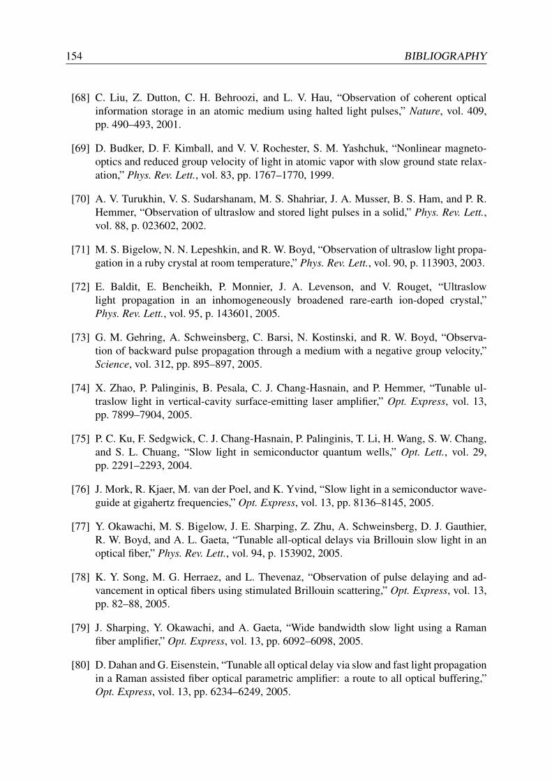
154 BIBLIOGRAPHY
[68] C. Liu, Z. Dutton, C. H. Behroozi, and L. V. Hau, “Observation of coherent opticalinformation storage in an atomic medium using halted light pulses,” Nature, vol. 409,pp. 490–493, 2001.
[69] D. Budker, D. F. Kimball, and V. V. Rochester, S. M. Yashchuk, “Nonlinear magneto-optics and reduced group velocity of light in atomic vapor with slow ground state relax-ation,” Phys. Rev. Lett., vol. 83, pp. 1767–1770, 1999.
[70] A. V. Turukhin, V. S. Sudarshanam, M. S. Shahriar, J. A. Musser, B. S. Ham, and P. R.Hemmer, “Observation of ultraslow and stored light pulses in a solid,” Phys. Rev. Lett.,vol. 88, p. 023602, 2002.
[71] M. S. Bigelow, N. N. Lepeshkin, and R. W. Boyd, “Observation of ultraslow light propa-gation in a ruby crystal at room temperature,” Phys. Rev. Lett., vol. 90, p. 113903, 2003.
[72] E. Baldit, E. Bencheikh, P. Monnier, J. A. Levenson, and V. Rouget, “Ultraslowlight propagation in an inhomogeneously broadened rare-earth ion-doped crystal,”Phys. Rev. Lett., vol. 95, p. 143601, 2005.
[73] G. M. Gehring, A. Schweinsberg, C. Barsi, N. Kostinski, and R. W. Boyd, “Observa-tion of backward pulse propagation through a medium with a negative group velocity,”Science, vol. 312, pp. 895–897, 2005.
[74] X. Zhao, P. Palinginis, B. Pesala, C. J. Chang-Hasnain, and P. Hemmer, “Tunable ul-traslow light in vertical-cavity surface-emitting laser amplifier,” Opt. Express, vol. 13,pp. 7899–7904, 2005.
[75] P. C. Ku, F. Sedgwick, C. J. Chang-Hasnain, P. Palinginis, T. Li, H. Wang, S. W. Chang,and S. L. Chuang, “Slow light in semiconductor quantum wells,” Opt. Lett., vol. 29,pp. 2291–2293, 2004.
[76] J. Mork, R. Kjaer, M. van der Poel, and K. Yvind, “Slow light in a semiconductor wave-guide at gigahertz frequencies,” Opt. Express, vol. 13, pp. 8136–8145, 2005.
[77] Y. Okawachi, M. S. Bigelow, J. E. Sharping, Z. Zhu, A. Schweinsberg, D. J. Gauthier,R. W. Boyd, and A. L. Gaeta, “Tunable all-optical delays via Brillouin slow light in anoptical fiber,” Phys. Rev. Lett., vol. 94, p. 153902, 2005.
[78] K. Y. Song, M. G. Herraez, and L. Thevenaz, “Observation of pulse delaying and ad-vancement in optical fibers using stimulated Brillouin scattering,” Opt. Express, vol. 13,pp. 82–88, 2005.
[79] J. Sharping, Y. Okawachi, and A. Gaeta, “Wide bandwidth slow light using a Ramanfiber amplifier,” Opt. Express, vol. 13, pp. 6092–6098, 2005.
[80] D. Dahan and G. Eisenstein, “Tunable all optical delay via slow and fast light propagationin a Raman assisted fiber optical parametric amplifier: a route to all optical buffering,”Opt. Express, vol. 13, pp. 6234–6249, 2005.
BIBLIOGRAPHY 155
[81] J. Sharping, Y. Okawachi, J. van Howe, C. Xu, Y. Wang, A. Willner, and A. Gaeta, “All-optical, wavelength and bandwidth preserving, pulse delay based on parametric wave-length conversion and dispersion,” Opt. Express, vol. 13, pp. 7872–7877, 2005.
[82] G. Lenz, B. J. Eggleton, C. K. Madsen, and R. E. Slusher, “Optical delay lines based onoptical filters,” IEEE J. Quantum Electron., vol. 37, pp. 525–532, 2001.
[83] M. L. Povinelli, S. G. Johnson, and J. D. Joannopoulos, “Slow-light, band-edge wave-guides for tunable time delays,” Opt. Express, vol. 13, pp. 7145–7159, 2005.
[84] Q. Xu, P. Dong, and M. Lipson, “Breaking the delay-bandwidth limit in a photonic struc-ture,” Nature Physics, vol. 3, pp. 406–410, 2005.
[85] F. Xia, L. Sekaric, and Y. Vlasov, “Ultracompact optical buffers on a silicon chip,” NaturePhotonics, vol. 1, pp. 65–71, 2007.
[86] A. Yariv, Y. Xu, R. K. Lee, and A. Scherer, “Coupled-resonator optical waveguide: Aproposal and analysis,” Opt. Lett., vol. 24, pp. 711–713, 1999.
[87] M. F. Yanik, W. Suh, Z. Wang, and S. Fan, “Stopping light in a waveguide with an all-optical analog of electromagnetically induced transparency,” Phys. Rev. Lett., vol. 93,p. 233903, 2004.
[88] H. Gersen, T. J. Karle, R. J. P. Engelen, W. Bogaerts, J. P. Korterik, N. F. van Hulst, T. F.Krauss, and L. Kuipers, “Real-space observation of ulstraslow light in photonic crystalwaveguides,” Phys. Rev. Lett., vol. 94, p. 073903, 2005.
[89] C. J. M. Smith, H. Benisty, S. Olivier, M. Rattier, C. Weisbuch, T. F. Krauss, R. M.De La Rue, R. Houdre, and U. Oseterle, “Low-loss channel waveguides with two-dimensional photonic crystal boundaries,” Appl. Phys. Lett., vol. 77, pp. 2813–2815,2000.
[90] H. Frandsen, L, A. Harpoth, P. I. Borel, M. Kristensen, S. S. Jensen, and O. Sigmund,“Broadband photonic crystal waveguide 60 bend obtained utilizing topology optimiza-tion,” Opt. Express, vol. 12, pp. 5916–5921, 2004.
[91] Y. Watanabe, N. Ikeda, Y. Sugimoto, Y. Takata, Y. Kitagawa, A. Mizutani, N. Ozaki, andK. Asakawa, “Topology optimization of waveguide bends with wide, flat bandwidth inair-bridge-type photonic crystal slabs,” Journ. of Appl. Phys., vol. 10, p. 113108, 2007.
[92] R. S. Jacobsen, A. V. Lavrinenko, L. H. Frandsen, C. Peucheret, B. Zsigri, G. Moulin,J. Fage-Pedersen, and P. I. Borel, “Direct experimental and numerical determination ofextremely high group indices in photonic crystal waveguides,” Opt. Express, vol. 13,pp. 7861–7871, 2005.
[93] L. H. Frandsen, A. V. Lavrinenko, J. Fage-Pedersen, and P. I. Borel, “Photonic crys-tal waveguides with semi-slow light and tailored dispersion properties,” Opt. Express,vol. 14, pp. 9444–9450, 2006.
156 BIBLIOGRAPHY
[94] S. Kubo, D. Mori, and T. Baba, “Low-group-velocity and low-dispersion slow light inphotonic crystal waveguides,” Opt. Lett., vol. 32, pp. 2981–2983, 2007.
[95] M. D. Settle, R. J. P. Engelen, M. Salib, A. Michaeli, L. Kuipers, and T. F. Krauss, “Flat-band slow light in photonic crystals featuring spatial pulse compression and terahertzbandwidth,” Opt. Express, vol. 15, pp. 219–226, 2007.
[96] D. Mori, S. Kubo, H. Sasaki, and T. Baba, “Experimantal demonstration of widebanddispersion-compensated slow light by a chirped photonic crystal directional coupler,”Opt. Express, vol. 15, pp. 5264–5270, 2007.
[97] M. Notomi, A. Shinya, K. Yamada, J. Takahashi, C. Takahashi, and I. Yokohama, “Struc-tural tuning of guiding modes of line-defect waveguides of silicon-on-insulator photoniccrystal slabs,” IEEE J. Quantum Electron., vol. 38, pp. 736–742, 2002.
[98] V. R. Almeida, Q. Xu, C. A. Barrios, and M. Lipson, “Guiding and confining light invoid nanostructure,” Opt. Lett., vol. 29, no. 11, pp. 1209–1211, 2004.
[99] C. Koos, L. Jacome, C. Poulton, J. Leuthold, and W. Freude, “Nonlinear silicon-on-insulator waveguides for all-optical signal processing,” Opt. Express, vol. 15, pp. 5976–1590, 2007.
[100] Y. A. Vlasov and S. J. McNab, “Coupling into the slow light mode in slab-type photoniccrystal waveguides,” Opt. Lett., vol. 31, pp. 50–52, 2006.
[101] W. P. Huang, “Coupled-mode theory for optical waveguides: an overview,”J. Opt. Soc. Am., vol. 11, pp. 963–983, 1994.
[102] H. A. Haus, W. P. Huang, S. Kawakami, and N. A. Whitaker, “Coupled-mode theory ofoptical waveguides,” J. Lightw. Technol., vol. LT-5, pp. 16–23, 1987.
[103] L. O’Faolain, T. P. White, D. O’Brien, X. Yuan, M. D. Settle, and T. F. Krauss, “Depen-dence of extrinsic loss on group velocity in photonic crystal waveguides,” Opt. Express,vol. 15, pp. 13129–13138, 2007.
[104] D. Marcuse, Theory of Dielectric Optical Waveguides. London: Academic Press, 1974.
[105] D. Marcuse, “Coupled power equations for backward waves,” IEEE Trans. MicrowaveTheory Tech., vol. MTT-20, pp. 541–546, 1972.
[106] B. S. Song, S. Noda, T. Asano, and Y. Akahane, “Ultra-high-Q photonic double-heterostructure nanocavity,” Nature Materials, vol. 4, pp. 207–210, 2005.
[107] Y. Akahane, T. Asano, B. S. Song, and S. Noda, “High-Q photonic nanocavity in a two-dimensional photonic crystal,” Nature, vol. 425, pp. 944–947, 2003.
[108] L. H. Frandsen, P. I. Borel, Y. X. Zhuang, A. Harpoth, M. Thorhauge, M. Kristensen,W. Bogaerts, P. Dumon, R. Baets, V. Wiaux, J. Wouters, and S. Beckx, “Ultralow-loss3-dB photonic crystal waveguide splitter,” Opt. Lett., vol. 29, pp. 1623–1625, 2004.
BIBLIOGRAPHY 157
[109] Y. Akahane, T. Asano, H. Takano, B. S. Song, Y. Takana, and S. Noda, “Two-dimensionalphotonic-crystal-slab channel-drop filter with flat-top response,” Opt. Express, vol. 13,pp. 2512–2530, 2005.
[110] F. S. S. Chien, Y. J. Hsu, W. F. Hsieh, and S. C. Cheng, “Dual wavelength demultiplex-ing by coupling and decoupling of photonic crystal waveguides,” Opt. Express, vol. 12,pp. 1119–1125, 2004.
[111] O. Painter, R. K. Lee, A. Scherer, A. Yariv, J. D. O’Brien, P. D. Dapkus, and I. Kim,“Two-dimensional photonic band-gap defect mode laser,” Science, vol. 284, pp. 1819–1821, 1999.
[112] W. d. Zhou, J. Sabarinathan, B. Kochman, E. Berg, O. Qasaimeh, S. Pang, and P. Bhat-tacharya, “Electrically injected single-defect photonic bandgap surface-emitting laser atroom temperature,” Electron. Lett., vol. 36, pp. 1541–1542, 2000.
[113] T. Tanabe, M. Notomi, S. Mitsugi, A. Shinya, and E. Kuramochi, “Fast bistable all-optical switch and memory on a silicon photonic crystal on-chip,” Opt. Lett., vol. 30,pp. 2575–2577, 2005.
[114] A. J. Lowery and J. Armstrong, “Orthogonal-frequency-division multiplexing for disper-sion compensation of long-haul optical systems,” Opt. Express, vol. 14, pp. 2079–2084,2006.
[115] T. L. Koch and R. C. Alferness, “Dispersion compensation by active predistorted signalsynthesis,” J. Lightw. Technol., vol. LT-3, pp. 800–805, 1985.
[116] J. H. Winters and R. D. Gitlin, “Electrical signal processing techniques in long-haulfiber-optic systems,” IEEE Trans. Commun., vol. 38, pp. 1439–1453, 1990.
[117] R. I. Killey, P. M. Watts, V. Mikhailov, M. Glick, and P. Bayvel, “Electronic dis-persion compensation by signal predistortion using digital processing and a dual-driveMachZehnder modulator,” IEEE Photon. Technol. Lett., vol. 17, pp. 714–716, 2005.
[118] J. X. Cai, K. M. Feng, A. E. Willner, V. Grubsky, D. S. Starodubov, and J. Feinberg, “Si-multaneous tunable dispersion compensation of many WDM channels using a samplednonlinearly chirped fiber Bragg grating,” IEEE Photon. Technol. Lett., vol. 11, pp. 1455–1457, 1999.
[119] M. Shirasaki, “Chromatic-dispersion compensator using virtually imaged phased array,”IEEE Photon. Technol. Lett., vol. 9, pp. 1598–1600, 1997.
[120] D. J. Moss, M. Lamont, S. McLaughlin, G. Randall, P. Colbourne, S. Kiran, and C. A.Hulse, “Tunable dispersion and dispersion slope compensators for 10 Gb/s using all-passmulticavity etalons,” IEEE Photon. Technol. Lett., vol. 15, pp. 730–732, 2003.
[121] C. K. Madsen, J. A. Walker, K. W. Goossen, T. N. Nielsen, and G. Lenz, “A tunabledispersion compensating MEMS all-pass filter,” IEEE Photon. Technol. Lett., vol. 12,pp. 651–653, 2000.
158 BIBLIOGRAPHY
[122] U. Peschel, T. Peschel, and F. Lederer, “A compact device for highly efficient dispersioncompensation in fiber transmission,” Appl. Phys. Lett., vol. 67, pp. 2111–2113, 1995.
[123] C. K. Madsen, G. Lenz, A. J. Bruce, M. A. Cappuzzo, L. T. Gomez, and R. E. R. E. Scotti,“Integrated all-pass filters for tunable dispersion and dispersion slope compensation,”IEEE Photon. Technol. Lett., vol. 11, pp. 1623–1625, 1999.
[124] K. Takiguchi, K. Jinguji, K. Okamoto, and Y. Ohmori, “Variable group-delay disper-sion equalizer using lattice-form programmable optical filter on planar lightwave circuit,”IEEE J. Sel. Top. Quantum Electron., vol. 2, pp. 270–276, 1996.
[125] C. R. Doerr, L. W. Stulz, S. Chandrasekhar, and R. Pafchek, “Colorless tunable disper-sion compensator with 400-ps/nm range integrated with a tunable noise filter,” IEEE Pho-ton. Technol. Lett., vol. 15, pp. 1258–1260, 2003.
[126] A. Yariv, D. Fekete, and D. M. Pepper, “Compensation for channel dispersion by nonlin-ear optical phase conjugation,” Opt. Lett., vol. 4, pp. 52–54, 1979.
[127] D. Mogilevtsev, T. A. Birks, and P. S. J. Russell, “Group-velocity dispersion in photoniccrystal fibers,” Opt. Lett., vol. 23, pp. 1662–1664, 1998.
[128] A. Y. Petrov and M. Eich, “Efficient approximation to calculate time delay and disper-sion in linearly chirped periodical microphotonic structures,” IEEE J. Quantum Electron.,vol. 41, pp. 1502–1509, 2005.
[129] W. J. Kim, W. Kuang, and J. D. OBrien, “Dispersion characteristics of photonic crystalcoupled resonator optical waveguides,” Opt. Express, vol. 11, pp. 3431–3437, 2003.
[130] Z. Zhu, A. M. C. Dawes, D. J. Gauthier, L. Zhang, and A. E. Willner, “Broadband SBSslow light in an optical fiber,” J. Lightw. Technol., vol. 25, pp. 201–206, 2007.
[131] Y. Okawachi, R. Salem, and A. L. Gaeta, “Continuous tunable delays at 10-Gb/s datarates using self-phase modulation and dispersion,” J. Lightw. Technol., vol. 25, pp. 3710–3715, 2007.
[132] F. Morichetti, A. Melloni, A. Breda, A. Canciamilla, C. Ferrari, and M. Martinelli,“A reconfigurable architecture for continuously variable optical slow-wave delay lines,”Opt. Express, vol. 15, pp. 17273–17282, 2007.
[133] L. Liao, A. Liu, D. Rubin, J. Basak, Y. Chetrit, H. Nguyen, R. Cohen, N. Izhaky, andM. Paniccia, “40Gbit/s silicon optical modulator for high-speed applications,” Elec-tron. Lett., vol. 43, p. 20072253, 2007.
[134] B. Bortnik, Y. C. Hung, H. Tazawa, B. J. Seo, J. Luo, A. K. Y. Jen, W. H. Steier,and H. R. Fetterman, “Electrooptic polymer ring resonator modulation up to 165GHz,”IEEE J. Sel. Top. Quantum Electron., vol. 13, pp. 104–110, 2007.
[135] D. Rezzonico, M. Jazbinsek, A. Guarino, O. P. Kwon, and P. Gunter, “Electro-opticcharon polymeric microring modulators,” Opt. Express, vol. 16, pp. 613–627, 2008.
BIBLIOGRAPHY 159
[136] E. M. McKenna, A. S. Lin, A. R. Mickelson, R. Dinu, and D. Jin, “Comparison of r33 val-ues for AJ404 films prepared with parallel plate and corona poling,” J. Opt. Soc. Am. B,vol. 24, pp. 2888–2892, 2007.
[137] B. Wang, T. Baehr-Jones, M. Hochberg, and A. Scherer, “Design and fabrication ofsegmented, slotted waveguides for electro-optic modulation,” Appl. Phys. Lett., vol. 91,p. 143109, 2007.
[138] Q. Xu, B. Schmidt, S. Pradhan, and M. Lipson, “Micrometre-scale silicon electro-opticmodulator,” Nature, vol. 435, pp. 325–327, 2005.
[139] B. Schmidt, Q. Xu, J. Shakya, S. Manipatruni, and M. Lipson, “Compact electro-opticmodulator on silicon-on-insulator substrates using cavities with ultra-small modal vol-umes,” Opt. Express, vol. 15, pp. 3140–3148, 2007.
[140] K. K. McLauchlan and S. T. Dunham, “Analysis of a compact modulator incorporatinga hybrid silicon/electro-optic polymer waveguide,” IEEE J. Sel. Top. Quantum Electron.,vol. 12, pp. 1455–1460, 2006.
[141] L. C. Andreani and D. Gerace, “Photonic-crystal slabs with a triangular lattice of trian-gular holes investigated using a guided-mode expansion method,” Phys. Rev. B, vol. 73,p. 235114, 2006.
[142] C. Koos, Nanophotonic Devices for Linear and Nonlinear Optical Signal Processing.PhD thesis, Universitat Karlsruhe (TH), 2008.
[143] M. Notomi, A. Shinya, S. Mitsugi, E. Kuramochi, and H. Y. Ryu, “Waveguides, res-onators and their coupled elements in photonic crystal slabs,” Opt. Express, vol. 12,pp. 1551–1561, 2004.
[144] W. Bogaerts, R. Baets, P. Dumon, V. Wiaux, S. Beckx, D. Taillaert, B. Luyssaert,J. van Campenhout, P. Bienstman, and D. van Thourhout, “Nanophotonic waveguidesin silicon-on-insulator fabricated with CMOS technology,” J. Lightw. Technol., vol. 23,pp. 401–412, 2005.
[145] A. D. Falco, L. OFaolain, and T. F. Krauss, “Dispersion control and slow light in slottedphotonic crystal waveguides,” Appl. Phys. Lett., vol. 92, p. 083501, 2008.
[146] W. Bogaerts, R. Baets, P. Dumon, V. Wiaux, S. Beckx, D. Taillaert, B. Luyssaert,J. Van Campenhout, P. Bienstmann, and D. Van Thourhout, “Nanophotonic wave-guides in silicon-on-insulator fabricated with CMOS technology,” J. Lightwave Technol.,vol. 23, no. 1, pp. 401–412, 2005.
[147] J. Canning, N. Skivesen, M. Kristensen, L. H. Frandsen, A. Lavrinenko, C. Martelli,and A. Tetu, “Mapping the broadband polarization properties of linear 2D SOI photoniccrystal waveguides,” Opt. Express, vol. 15, pp. 15603–15614, 2007.
[148] S. L. McCall, P. M. Platzmann, R. Dalichaouch, D. Smith, and S. Schultz, “Microwavepropagation in two-dimensional dielectric lattices,” Phys. Rev. Lett., vol. 67, pp. 2017–2020, 1991.
160 BIBLIOGRAPHY
[149] C. Jin, b. Cheng, B. Man, Z. Li, and D. Zhang, “Two-dimensional dodecagonal anddecagonal quasiperiodic photonic crystals in the microwave region,” Phys. Rev. B,vol. 61, p. 10762, 2000.
[150] D. R. Solli, C. F. McCormick, R. Y. Chiao, and J. M. Hickmann, “Experimental demon-stration of photonic crystal waveplates,” Appl. Phys. Lett., vol. 82, pp. 1036–1038, 2003.
[151] E. Ozbay, M. Bayindir, I. Bulu, and E. Cubukcu, “Investigation of localized coupled-cavity modes in two-dimensional photonic bandgap structures,” IEEE J. Quantum Elec-tron., vol. 38, pp. 837–843, 2002.
[152] F. Cuesta, A. Griol, A. Martinez, and J. Marti, “Experimental demonstration of photoniccrystal directional coupler at microwave frequencies,” Electron. Lett., vol. 39, pp. 455–456, 2003.
[153] A. A. Chabanov, M. Stoytchev, and A. Z. Genack, “Statistical signatures of photon lo-calization,” Nature, vol. 404, pp. 850–853, 2000.
[154] R. A. Shelby, D. R. Smith, and S. Schultz, “Experimental verification of a negative indexof refraction,” Science, vol. 292, pp. 77–79, 2001.
[155] E. Cubukcu, K. Aydin, E. Ozbay, S. Foteinopoulou, and C. M. Soukoulis, “Negativerefraction by photonic crystals,” Nature, vol. 423, pp. 604–605, 2003.
[156] P. V. Parimi, W. T. Lu, P. Vodo, J. Sokoloff, J. S. Derov, and S. Sridhar, “Negative refrac-tion and left-handed electromagnetism in microwave photonic crystals,” Phys. Rev. Lett.,vol. 92, p. 127401, 2004.
[157] Z. Lu, J. A. Murakowski, C. A. Schuetz, S. Shi, G. J. Schneider, and D. W. Prather,“Three-dimensional subwavelength imaging by a photonic-crystal flat lens using negativerefraction at microwave frequencies,” Phys. Rev. Lett., vol. 95, p. 153901, 2005.
[158] T. J. Karle, Y. J. Chai, C. N. Morgan, I. H. White, and T. F. Krauss, “Observation of pulsecompression in photonic crystal coupled cavity waveguides,” J. Lightw. Technol., vol. 22,pp. 514–519, 2004.
[159] D. Mori and T. Baba, “Wideband and low dispersion slow light by chirped photoniccrystal coupled waveguide,” Opt. Express, vol. 13, pp. 9398–9408, 2005.
[160] CST Microwave Studio, http://www.cst.com/.
[161] RSOFT FullWAVE, http://www.rsoftdesign.com/.
[162] MIT photonic bands, http://ab-initio.mit.edu/wiki/index.php/MIT Photonic Bands/.
[163] Guided mode expansion, http://fisicavolta.unipv.it/dipartimento/ricerca/Fotonici/.
[164] G. Lecamp, J. P. Hugonin, and P. Lalanne, “Theoretical and computational concepts forperiodic optical waveguides,” Opt. Express, vol. 15, pp. 11052–11060, 2007.

BIBLIOGRAPHY 161
[165] G. F. Engen and C. A. Hoer, “Thru-reflect-line: An improved technique for calibratingthe dual six-port automatic network analyzer,” IEEE Trans. Microwave Theory Tech.,vol. MTT-27, pp. 987–993, 1979.

162 BIBLIOGRAPHY
Acknowledgments
This thesis is the result of my work at the Institute of High-Frequency and Quantum Electronics(IHQ) at the University of Karlsruhe (TH), Germany. We acknowledge the support by theDeutsche Forschungsgemeinschaft (DFG) in the framework of the Priority Program SP 1113“Photonic Crystals”, by the Deutsche Telekom Stiftung, and by the European FP6 Network ofExcellence ePIXnet.
At this point I also want to thank all the people who have helped in making this work asuccess.
First of all, I want to thank my supervisors Prof. Wolfgang Freude and Prof. Jurg Leuthold.They have always supported me, brought forward inspiring ideas, and have given me plentyof room for independant work. My first supervisor, Prof. Wolfgang Freude, I want to thankfor his great analytic expertise that always helped to get technical issues to the point and findsolutions, his thoroughness that prevented mistakes to creep in, and for his great helpfulnessand his always open door where I could step in at any time. Our institute head, Prof. JurgLeuthold, I especially want to thank for his vision that helped to see the big picture and hissteadfast optimism to bring small commencements finally to a success.
Prof. Lucio Claudio Andreani of the University of Pavia, Italy, I want to thank for thecollaboration in the simulation of band diagrams and of disorder-induced losses with the guidedmode expansion (GME) method. He provided and advanced his GME code for our applications,and many helpful discussions took place.
Dr. Alexander Petrov, University of Hamburg-Harburg, I thank for the collaboration anddiscussion on broadband slow-light photonic crystal waveguides and for his help in the firstdesign that we realized in the microwave model.
Dr. Pieter Dumon of the Interuniversity Microelectronics Center (IMEC), Leuven, Belgium,I thank for the help in the mask design and for his support in the successful fabrication of oursilicon-on-insulator (SOI) devices in the ePIXnet framework.
Peter Pfundstein of the Laboratory for Microscopy (LEM), University of Karlsruhe, I wantto thank for conducting the scanning electron microscope pictures of our SOI samples.
Prof. Uli Lemmer and Christian Kayser of the Light Technology Institute (LTI), Universityof Karlsruhe, I thank for giving access to their clean room and for the instructions on spin-coating.
163
164 Acknowledgments
My former colleague Dr. Christian Koos I especially thank for the countless helpful dis-cussions in numerous fields, for the collaboration in the SOI design and the provision of hischaracterization setup, and for his deep knowledge he was always willing to share. My formercolleague Dr. Christopher Poulton I thank for the discussions on the fundamentals of photoniccrystals and of disorder effects, and for the collaboration on numerical modeling.
The mechanical workshop, Hans Burger, Manfred Hirsch, Werner Hohne, Oswald Speckand the apprentices I thank for the fabrication of the microwave model structures and for theexecution of all kinds of other technical tasks. Oswald Speck of the packaging lab I thank forthe great support in wafer cleaving, lapping and handling.
Andrej Marculescu I thank for his extensive help in all kinds of computer issues, and for theprovision of optical measurement equipment. Philipp Vorreau I thank for the discussions aboutand the provision of microwave and optical measurement equipment. Thomas Vallaitis I wantto thank for the discussions concerning silicon photonics and semiconductors.
Many thanks to all the students who have contributed to our work: Michael Waldow, MireiaMonllor Tormos, Irene Netsch, Simon Schneider and Christoph Heine.
For the great collaboration I want to thank all my colleagues at IHQ, Rene Bonk, Dr. GunnarBottger, Dr. Shunfeng Li, Jingshi Li, Andrej Marculescu, Moritz Roger, Dr. Stelios Sygletos,Thomas Vallaitis, Philipp Vorreau, and Jin Wang and my former colleagues Dr. Guy-AimarChakam, Dr. Richard Ell, Anastasiya Golovina, Dr. Martin Hugelmann, Dr. Philipp Hugel-mann, Lenin Jacome, Dr. Christian Koos, Dr. Ayan Maitra, Dr. Christopher Poulton, Dr.Wolfgang Seitz, Oleksiy Shulika and Dr. Philipp Wagenblast.
Many thanks to our secretaries, Bernadette Lehmann and Dagmar Goldmann, for the helpin administrative matters, and to Ilse Kober for the technical artwork. Thanks to Peter Frey andWerner Podszus for the support in electrical and technical matters.
Besides the work-related concerns, I also want to thank all my colleagues for the personalfriendships, for the good working climate, for the encouragement, and for the times of relaxationand fun. Moritz and Gunnar, it is a pleasure to share the office with you.
Many thanks to my parents Willi and Heidemarie Brosi and to my family for their support.I also want to thank my girlfriend Christiane Sutter for all her help, her care and her affection.
Finally, I thank my Saviour Jesus, who is the reason of my life. “For from him and throughhim and to him are all things. To him be the glory for ever.” (Romans 11:36, the Bible)

List of Own Publications
PatentsP1 Koos, C.; Leuthold, J.; Freude, W., Brosi, J.-M.: Elektro-optisches Bauteil mit transpar-
enten Elektroden, kleiner Betriebsspannung und hoher Grenzfrequenz, file numbers DE10 2006 045 102 A1, WO 2008/034559 A1
Journal PapersJ3 Brosi J.-M.; Koos C.; Andreani L. C.; Waldow M.; Leuthold J.; Freude W.: High-speed
low-voltage electro-optic modulator with a polymer-infiltrated silicon photonic crystalwaveguide, Opt. Expr. 16 (2008) 4177–4191
J2 Brosi J.-M.; Leuthold J.; Freude W.: Microwave-frequency experiments validate opticalsimulation tools and demonstrate novel dispersion-tailored photonic crystal waveguides,J. Lightw. Technol. 25 (2007) 2502–2510
J1 Stalzer H.; Cosceev A.; Surgers C.; v. Lohneysen H.; Brosi J.-M.; Chakam G.-A.; FreudeW.: Inhomogeneous magnetization of a superconducting film measured with a gradiome-ter, Appl. Phys. Lett. 84 (2004) 1522–1524
Book ChapterB1 Freude, W.; Chakam, G.-A.; Brosi, J.-M.; Koos, C.: Microwave Modelling of Photonic
Crystals. In: Busch, K.; Lolkes, S.; Wehrspohn, R.; Foll, H. (Eds.): Photonic Crystals– Advances in Design, Fabrication, and Characterization. Wiley VCH, Berlin 2004,pp.198–214
Conference ContributionsC20 Brosi J.-M.; Koos C.; Andreani L. C.; Dumon P.; Baets R.; Leuthold J.; Freude W.:
100 Gbit/s / 1 V Optical Modulator With Slotted Slow-Light Polymer-Infiltrated SiliconPhotonic Crystal. Slow and Fast Light, OSA Topical Meeting, Boston MA, USA; July13-16, 2008
165
166 List of Own Publications
C19 Freude W.; Brosi J.-M.; Koos C.; Vorreau P.; Andreani L. C.; Dumon P.; Baets R.; Es-embeson B.; Biaggio I.; Michinobu T.; Diederich F.; Leuthold J.: Silicon-organic hybrid(SOH) devices for nonlinear optical signal processing. Proc. 10th Intern. Conf. onTransparent Optical Networks (ICTON’08), June 22–26, 2008, Athens, Greece (invited)
C18 Brosi J.-M.; Freude W.; Leuthold J.: Schneller elektro-optischer Modulator als silizium-organische Hybridstruktur auf der Basis von photonischen Kristallen. VDE-ITG Work-shop der Fachgruppe 5.3.1, Kiel, Germany, June 12–13, 2008.
C17 Freude W.; Brosi J.-M.; Koos C.; Vorreau P.; Andreani L. C.; Dumon P.; Baets R.;Esembeson B.; Biaggio I.; Michinobu T.; Diederich F.; Leuthold J.: Silicon photonicsmeets nonlinear organic materials. Proc. COST-MP0702 Workshop and WG Meeting,Warsaw, Poland, April 28–29, 2008. Paper P2.3.1, pp. 60–62
C16 Koos C.; Brosi J.; Waldow M.; Freude W.; Leuthold J.: Silicon-on-insulator modulatorsfor next-generation 100 Gbit/s-Ethernet. Proc. 33th European Conf. Opt. Commun.(ECOC’07), Berlin, Germany; September 16–20, 2007, Paper P056
C15 Bottger G.; Brosi J.-M.; Maitra A.; Wang J.; Petrov A.Y.; Eich M.; Leuthold J.; Freude,W.: Broadband slow light and nonlinear switching devices. Proc. Progress in Electro-magnetics Research Symposium 2006 (PIERS’07), Beijing, China; March 26–30, 2007,pp.1338-1342 (invited)
C14 Freude, W.; Fujii, M.; Koos, C.; Brosi, J.; Poulton, C. G.; Wang, J.; Leuthold, J.: WaveletFDTD methods and applications in nano-photonics, 386th WE Heraeus Seminar ‘Com-putational Nano-Photonics’, Bad Honnef, February 25–28, 2007 (invited)
C13 Brosi J.-M., Freude W., Leuthold J.: Broadband Slow Light in a Photonic Crystal LineDefect Waveguide. Proc. Slow and Fast Light, OSA Topical Meeting, OSA Headquarters,Washington DC, USA; July 23-26, 2006
C12 Freude W.; Brosi J.: Finite-difference time-domain and beam propagation methods forMaxwell’s equations. 4-hours lecture with hands-on demonstrations given as part of theCOST P11 Training School ’Modelling and Simulation Techniques for Linear, Nonlinearand Active Photonic Crystals’; University of Nottingham, UK; June, 2006
C11 Freude, W.; Poulton, C. G.; Koos, C.; Brosi, J.; Fujii, M.; Pfrang, A.; Schimmel, Th.;Muller, M.; Leuthold, J.: Nanostrip and photonic crystal waveguides: The modellingof imperfections, Proc. 15th International Workshop on Optical Waveguide Theory andNumerical Modelling (OWTNM’06), Varese, Italy, April 20–21, 2006, pp. 1–2 (invited)
C10 Freude W.; Poulton C.; Koos C.; Brosi J.; Fujii M.; Muller M.; Leuthold J.; Pfrang A.;Schimmel Th.: Nano-optical waveguide devices with random deformations and nonlin-earities. Proc. 3rd Intern. Conf. on Materials for Advanced Technologies (ICMAT’05),Symposium F: Nano-Optics and Microsystems, Singapore; July 3–8, 2005, Paper F-2-N3(invited)
List of Own Publications 167
C9 Brosi J.; Poulton C.; Freude W.: Microwave modelling of disorder in photonic crys-tal slab waveguides. Proc. Spring Meeting, Deutsche Physikalische Gesellschaft, DPGQuantum Optics Section, Berlin, Germany; March 2005
C8 Freude, W.; Poulton, C.; Brosi, J.; Koos, C.; Glockler, F.; Wang, J.; Fujii, M.: Integratedoptical waveguide devices: Design, modeling and fabrication, Proc. 16th Asia PacificMicrowave Conference (APMC’04), New Delhi, India, December 15–18, 2004 (invited)
C7 Freude, W.; Brosi, J.; Glockler, F.; Koos, C.; Poulton, C.; Wang, J.; Fujii, M.: High-indexoptical waveguiding structures, Conf. Proc. Optical Society of America Annual Meeting(OSA 2004), Rochester (NY), USA, October 10–14, 2004, paper TuS1 (invited)
C6 Freude, W.; Poulton, C.; Koos, C.; Brosi, J.; Glockler, F.; Wang, J.; Chakam, G.-A.;Fujii, M.: Design and fabrication of nanophotonic devices, Proc. 6th Intern. Conf. onTransparent Optical Networks (ICTON’04), July 4–8, 2004, Wroclaw, Poland. Mo.A.4vol. 1 pp. 4–9 (invited)
C5 Brosi, J.; Chakam, G.-A.; Poulton, C.; Freude, W.: Microwave Modeling of IntegratedOptical Devices. 323th WE Heraeus Seminar ‘From Photonic Crystals to Metamaterials- Artificial Materials in Optics’, Bad Honnef, April 26–30, 2004
C4 Poulton C.; Brosi J.; Koos C.; Glockler F.; Wang J.; Fujii M.; Freude W.: Simulation,Design and Fabrication of Integrated Optical Devices. Proc. Third Joint Symposiumon Opto- and Microelectronic Devices and Circuits (SODC’04), Wuhan, China; March21–26, 2004, pp. 33–35
C3 Stalzer, H.; Cosceev, A.; Surgers, C.; v. Lohneysen, H.; Brosi, J.-M.; Chakam, G.-A.;Freude, W.: Proximity-Effekt in supraleitenden Nb/Ag- und Nb/Ag/Fe-Schichtpaketen.Spring Meeting of the German Physical Society, Regensburg, March 8–12, 2004
C2 Freude, W.; Brosi, J.-M.; Chakam, G.-A.; Glockler, F.; Koos, C.; Poulton, C.; Wang,J.: Modelling and design of nanophotonic devices, URSI Kleinheubacher Tagung, Mil-tenberg, Germany; September/October 2003 (invited)
C1 Poulton, C.; Brosi, J.; Glockler, F.; Koos, C.; Wang, J.; Freude, W.; Ilin, K.; SiegelM.; Fujii, M.: Modelling, design and realisation of SOI-based nanophotonic devices;Conference on Functional Nanostructures 2003 (CFN03), Karlsruhe, Germany. Septem-ber/October 2003

168 List of Own Publications

Curriculum Vitae
Jan-Michael Brosiborn March 21, 1978in Filderstadt, GermanyCitizenship: German
Education04/03–8/08 Dr.-Ing., Electrical Engineering, Institute of High-Frequency and Quantum Elec-
tronics (IHQ), University of Karlsruhe, Germany.
08/01–08/02 M.Sc., Electrical Engineering, Georgia Institute of Technology, Atlanta, USA.Specialization in Optics and Photonics, Microwave Engineering.
10/98–03/03 Studies of Electrical Engineering, University of Karlsruhe, Germany.Specialization in Optical Telecommunications.
Experience08/02–10/02 Internship at Lucent Technologies, Nurnberg, Germany.
Work on polarization mode dispersion in optical fibers.
01/02–8/02 Teaching assistant for course Electromagnetics, Georgia Institute of Technology,Atlanta, USA.
10/99–02/01 Teaching assistant for courses Electrophysics and Electronic Circuits, Universityof Karlsruhe, Germany.
169

170 Curriculum Vitae
07/98–09/98 Internship at Kolbenschmidt, Neckarsulm, Germany.Training in the mechanical workshop and in various electronic labs.
07/97–06/98 Civillian Service, District hospital Bad Friedrichshall, Germany.
Scholarships and Awards02/2005 Ph.D. scholarship of the Deutsche Telekom Stiftung (3 years).
05/2001 Study scholarship of Nortel Networks (3 years).
01/2001 Fulbright travel grant for the Georgia Institute of Technology, Atlanta.
10/2000 Scholarship for the exchange program with the Georgia Institute of Technology, At-lanta.
09/2000 Pre-degree award of the faculty of electrical engineering of the University of Karlsruhe

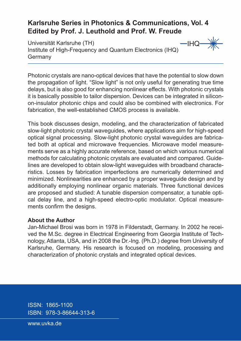
www.uvka.de
ISBN: 978-3-86644-313-6ISSN: 1865-1100 Ja
n-M
icha
el B
rosi
S
low
-Lig
ht P
C D
evic
es fo
r Hig
h-S
peed
Opt
ical
Sig
nal P
roce
ssin
g
4
Karlsruhe Series in Photonics & Communications, Vol. 4Edited by Prof. J. Leuthold and Prof. W. FreudeUniversität Karlsruhe (TH)Institute of High-Frequency and Quantum Electronics (IHQ)Germany
Karlsruhe Series in Photonics & Communications, Vol. 4
Photonic crystals are nano-optical devices that have the potential to slow down the propagation of light. “Slow light” is not only useful for generating true time delays, but is also good for enhancing nonlinear effects. With photonic crystals it is basically possible to tailor dispersion. Devices can be integrated in silicon-on-insulator photonic chips and could also be combined with electronics. For fabrication, the well-established CMOS process is available.
This book discusses design, modeling, and the characterization of fabricated slow-light photonic crystal waveguides, where applications aim for high-speed optical signal processing. Slow-light photonic crystal waveguides are fabrica-ted both at optical and microwave frequencies. Microwave model measure-ments serve as a highly accurate reference, based on which various numerical methods for calculating photonic crystals are evaluated and compared. Guide-lines are developed to obtain slow-light waveguides with broadband characte-ristics. Losses by fabrication imperfections are numerically determined and minimized. Nonlinearities are enhanced by a proper waveguide design and by additionally employing nonlinear organic materials. Three functional devices are proposed and studied: A tunable dispersion compensator, a tunable opti-cal delay line, and a high-speed electro-optic modulator. Optical measure-ments confirm the designs.
About the AuthorJan-Michael Brosi was born in 1978 in Filderstadt, Germany. In 2002 he recei-ved the M.Sc. degree in Electrical Engineering from Georgia Institute of Tech-nology, Atlanta, USA, and in 2008 the Dr.-Ing. (Ph.D.) degree from University of Karlsruhe, Germany. His research is focused on modeling, processing and characterization of photonic crystals and integrated optical devices.
Jan-Michael Brosi
Slow-Light Photonic Crystal Devices for High-SpeedOptical Signal Processing