SLOS712I –JANUARY 2011–REVISED OCTOBER … · -140-130-120-110-100-90-80-70-60-50-40 10k 100k...
59
-140 -130 -120 -110 -100 -90 -80 -70 -60 -50 -40 10k 100k 1M 10M Harmonic Distortion - dBc f - Frequency - Hz V = 2.7 V, G = 1, V = 1 Vpp, R = 0 , R = 1 k S OUT F L W W HD 3 HD 2 Product Folder Sample & Buy Technical Documents Tools & Software Support & Community Reference Design An IMPORTANT NOTICE at the end of this data sheet addresses availability, warranty, changes, use in safety-critical applications, intellectual property matters and other important disclaimers. PRODUCTION DATA. OPA836, OPA2836 SLOS712I – JANUARY 2011 – REVISED OCTOBER 2016 OPAx836 Very-Low-Power, Rail-to-Rail Out, Negative Rail In, Voltage-Feedback Operational Amplifiers 1 1 Features 1• Low Power: – Supply Voltage: 2.5 V to 5.5 V – Quiescent Current: 1 mA (Typical) – Power Down Mode: 0.5 μA (Typical) • Bandwidth: 205 MHz • Slew Rate: 560 V/μs • Rise Time: 3 ns (2 V STEP ) • Settling Time (0.1%): 22 ns (2 V STEP ) • Overdrive Recovery Time: 60 ns • SNR: 0.00013% (–117.6 dBc) at 1 kHz (1 V RMS ) • THD: 0.00003% (–130 dBc) at 1 kHz (1 V RMS ) • HD 2 /HD 3 : –85 dBc/–105 dBc at 1 MHz (2 V PP ) • Input Voltage Noise: 4.6 nV/√Hz (f = 100 kHz) • Input Offset Voltage: 65 μV (±400-μV Maximum) • CMRR: 116 dB • Output Current Drive: 50 mA • RRO: Rail-to-Rail Output • Input Voltage Range: –0.2 V to +3.9 V (5-V Supply) • Operating Temperature Range: –40°C to +125°C 2 Applications • Low-Power Signal Conditioning • Audio ADC Input Buffers • Low-Power SAR and ΔΣ ADC Drivers • Portable Systems • Low-Power Systems • High-Density Systems 3 Description The OPA836 and OPA2836 devices (OPAx836) are single- and dual-channel, ultra-low power, rail-to-rail output, negative-rail input, voltage-feedback (VFB) operational amplifiers designed to operate over a power-supply range of 2.5 V to 5.5 V with a single supply, or ±1.25 V to ±2.75 V with a dual supply. Consuming only 1 mA per channel and a unity-gain bandwidth of 205 MHz, these amplifiers set an industry-leading power-to-performance ratio for rail- to-rail amplifiers. For battery-powered, portable applications where power is of key importance, the low-power consumption and high-frequency performance of the OPA836 and OPA2836 devices offer performance- versus-power capability that is not attainable in other devices. Coupled with a power-savings mode to reduce current to < 1.5 μA, these devices offer an attractive solution for high-frequency amplifiers in battery-powered applications. The OPA836 RUN package option includes integrated gain-setting resistors for the smallest possible footprint on a printed-circuit board (approximately 2.00 mm × 2.00 mm). By adding circuit traces on the PCB, gains of +1, –1, –1.33, +2, +2.33, –3, +4, –4, +5, –5.33, +6.33, –7, +8 and inverting attenuations of –0.1429, –0.1875, –0.25, –0.33, –0.75 can be achieved. See Table 3 and Table 4 for details. The OPA836 and OPA2836 devices are characterized for operation over the extended industrial temperature range of –40°C to +125°C. Device Information (1) PART NUMBER PACKAGE BODY SIZE (NOM) OPA836 SOT-23 (6) 2.90 mm × 1.60 mm WQFN (10) 2.00 mm × 2.00 mm OPA2836 SOIC (8) 4.90 mm × 3.91 mm VSSOP (10) 3.00 mm × 3.00 mm UQFN (10) 2.00 mm × 2.00 mm WQFN (10) 2.00 mm × 2.00 mm (1) For all available packages, see the package option addendum at the end of the data sheet. Harmonic Distortion vs Frequency
Transcript of SLOS712I –JANUARY 2011–REVISED OCTOBER … · -140-130-120-110-100-90-80-70-60-50-40 10k 100k...

-140
-130
-120
-110
-100
-90
-80
-70
-60
-50
-40
10k 100k 1M 10M
Harm
on
ic D
isto
rtio
n -
dB
c
f - Frequency - Hz
V = 2.7 V,
G = 1,V = 1 Vpp,
R = 0 ,
R = 1 k
S
OUT
F
L
W
W
HD3
HD2
Product
Folder
Sample &Buy
Technical
Documents
Tools &
Software
Support &Community
ReferenceDesign
An IMPORTANT NOTICE at the end of this data sheet addresses availability, warranty, changes, use in safety-critical applications,intellectual property matters and other important disclaimers. PRODUCTION DATA.
OPA836, OPA2836SLOS712I –JANUARY 2011–REVISED OCTOBER 2016
OPAx836 Very-Low-Power, Rail-to-Rail Out, Negative Rail In, Voltage-FeedbackOperational Amplifiers
1
1 Features1• Low Power:
– Supply Voltage: 2.5 V to 5.5 V– Quiescent Current: 1 mA (Typical)– Power Down Mode: 0.5 µA (Typical)
• Bandwidth: 205 MHz• Slew Rate: 560 V/µs• Rise Time: 3 ns (2 VSTEP)• Settling Time (0.1%): 22 ns (2 VSTEP)• Overdrive Recovery Time: 60 ns• SNR: 0.00013% (–117.6 dBc) at 1 kHz (1 VRMS)• THD: 0.00003% (–130 dBc) at 1 kHz (1 VRMS)• HD2/HD3: –85 dBc/–105 dBc at 1 MHz (2 VPP)• Input Voltage Noise: 4.6 nV/√Hz (f = 100 kHz)• Input Offset Voltage: 65 µV (±400-µV Maximum)• CMRR: 116 dB• Output Current Drive: 50 mA• RRO: Rail-to-Rail Output• Input Voltage Range: –0.2 V to +3.9 V
(5-V Supply)• Operating Temperature Range:
–40°C to +125°C
2 Applications• Low-Power Signal Conditioning• Audio ADC Input Buffers• Low-Power SAR and ΔΣ ADC Drivers• Portable Systems• Low-Power Systems• High-Density Systems
3 DescriptionThe OPA836 and OPA2836 devices (OPAx836) aresingle- and dual-channel, ultra-low power, rail-to-railoutput, negative-rail input, voltage-feedback (VFB)operational amplifiers designed to operate over apower-supply range of 2.5 V to 5.5 V with a singlesupply, or ±1.25 V to ±2.75 V with a dual supply.Consuming only 1 mA per channel and a unity-gainbandwidth of 205 MHz, these amplifiers set anindustry-leading power-to-performance ratio for rail-to-rail amplifiers.
For battery-powered, portable applications wherepower is of key importance, the low-powerconsumption and high-frequency performance of theOPA836 and OPA2836 devices offer performance-versus-power capability that is not attainable in otherdevices. Coupled with a power-savings mode toreduce current to < 1.5 μA, these devices offer anattractive solution for high-frequency amplifiers inbattery-powered applications.
The OPA836 RUN package option includesintegrated gain-setting resistors for the smallestpossible footprint on a printed-circuit board(approximately 2.00 mm × 2.00 mm). By addingcircuit traces on the PCB, gains of +1, –1, –1.33, +2,+2.33, –3, +4, –4, +5, –5.33, +6.33, –7, +8 andinverting attenuations of –0.1429, –0.1875, –0.25,–0.33, –0.75 can be achieved. See Table 3 andTable 4 for details.
The OPA836 and OPA2836 devices arecharacterized for operation over the extendedindustrial temperature range of –40°C to +125°C.
Device Information(1)
PART NUMBER PACKAGE BODY SIZE (NOM)
OPA836SOT-23 (6) 2.90 mm × 1.60 mmWQFN (10) 2.00 mm × 2.00 mm
OPA2836
SOIC (8) 4.90 mm × 3.91 mmVSSOP (10) 3.00 mm × 3.00 mmUQFN (10) 2.00 mm × 2.00 mmWQFN (10) 2.00 mm × 2.00 mm
(1) For all available packages, see the package option addendumat the end of the data sheet.
Harmonic Distortion vs Frequency

2
OPA836, OPA2836SLOS712I –JANUARY 2011–REVISED OCTOBER 2016 www.ti.com
Product Folder Links: OPA836 OPA2836
Submit Documentation Feedback Copyright © 2011–2016, Texas Instruments Incorporated
Table of Contents1 Features .................................................................. 12 Applications ........................................................... 13 Description ............................................................. 14 Revision History..................................................... 25 OPA836-Related Devices ...................................... 46 Pin Configuration and Functions ......................... 47 Specifications......................................................... 6
7.1 Absolute Maximum Ratings ...................................... 67.2 ESD Ratings.............................................................. 67.3 Recommended Operating Conditions....................... 67.4 Thermal Information: OPA836 .................................. 67.5 Thermal Information: OPA2836 ................................ 77.6 Electrical Characteristics: VS = 2.7 V........................ 77.7 Electrical Characteristics: VS = 5 V........................... 97.8 Typical Characteristics ............................................ 12
8 Detailed Description ............................................ 248.1 Overview ................................................................. 248.2 Functional Block Diagrams ..................................... 24
8.3 Feature Description................................................. 248.4 Device Functional Modes........................................ 27
9 Application and Implementation ........................ 309.1 Application Information............................................ 309.2 Typical Applications ................................................ 36
10 Power Supply Recommendations ..................... 4011 Layout................................................................... 40
11.1 Layout Guidelines ................................................. 4011.2 Layout Example .................................................... 41
12 Device and Documentation Support ................. 4212.1 Device Support .................................................... 4212.2 Related Links ........................................................ 4212.3 Receiving Notification of Documentation Updates 4212.4 Community Resources.......................................... 4212.5 Trademarks ........................................................... 4212.6 Electrostatic Discharge Caution............................ 4212.7 Glossary ................................................................ 42
13 Mechanical, Packaging, and OrderableInformation ........................................................... 43
4 Revision HistoryNOTE: Page numbers for previous revisions may differ from page numbers in the current version.
Changes from Revision H (September 2016) to Revision I Page
• Changed text in sections throughout the data sheet to be more clear and concise .............................................................. 1• Changed "RG = ∞Ω (open)" to "RG = open".......................................................................................................................... 32• Changed "gain tracking is superior to using" to "gain drift is superior to the drift with"........................................................ 33• Changed "results in degraded harmonic distortion" to "increases the harmonic distortion" ............................................... 37• Deleted "A 10-Ω series resistor can be inserted between the capacitor and the noninverting pin to isolate the
capacitance." ........................................................................................................................................................................ 38
Changes from Revision G (October 2015) to Revision H Page
• Changed "Type" column header to "I/O" on Pin Functions table .......................................................................................... 5• Reformatted header rows in Thermal Information: OPA836 and Thermal Information: OPA2836 tables ............................ 6• Reformatted Thermal Information table note ......................................................................................................................... 6• Reformatted Thermal Information table note ......................................................................................................................... 7• Deleted the word "linear" from Output section parameters in Electrical Characteristics VS = 2.7 V table ............................ 7• Deleted the word "linear" from Output section parameters in Electrical Characteristics VS = 5 V table ............................... 9• Reformatted Development Support subsection ................................................................................................................... 42• Reformatted Related Documentation section ...................................................................................................................... 42• Added Receiving Notification of Documentation Updates section ...................................................................................... 42
Changes from Revision E (September 2013) to Revision F Page
• Changed Features section ..................................................................................................................................................... 1• Added Pin Configuration and Functions section, ESD Ratings table, Feature Description section, Device Functional
Modes, Application and Implementation section, Power Supply Recommendations section, Layout section, Deviceand Documentation Support section, and Mechanical, Packaging, and Orderable Information section .............................. 1

3
OPA836, OPA2836www.ti.com SLOS712I –JANUARY 2011–REVISED OCTOBER 2016
Product Folder Links: OPA836 OPA2836
Submit Documentation FeedbackCopyright © 2011–2016, Texas Instruments Incorporated
• Changed Device Comparison Table....................................................................................................................................... 4• Changed Pin Functions table ................................................................................................................................................. 5• Changed Open Loop Gain vs Frequency graph................................................................................................................... 15• Changed Input Referred Noise vs Frequency graph ........................................................................................................... 15• Changed Open Loop Gain vs Frequency graph ................................................................................................................. 21• Changed Input Referred Noise vs Frequency graph............................................................................................................ 21
Changes from Revision D (October 2011) to Revision E Page
• Added OPA2836 RMC package to document........................................................................................................................ 1• Added RMC pin definitions to Pin Functions table ................................................................................................................. 5• Deleted Packaging/Ordering Information table, leaving only note to POA............................................................................. 6• Added OPA2836 RMC package to Thermal Information table............................................................................................... 7
Changes from Revision C (September 2011) to Revision D Page
• Removed Product Preview from OPA835IRUNT and OPA835IRUNR.................................................................................. 4• Removed Product Preview from OPA836IRUNT and OPA836IRUNR.................................................................................. 6• Changed typical value for resistor temperature coefficien parameter from TBD to < 10 ....................................................... 9• Changed "quiescent operating current" parameter to "quiescent operating current per amplifier" ........................................ 9• Changed resistor temperature coefficient typical value from TBD to < 10........................................................................... 11• Changed "quiescent operating current" to "quiescent operating current per amplifier" ....................................................... 11
Changes from Revision B (May 2011) to Revision C Page
• Added the "The OPA836 RUN package..." text to the Description ........................................................................................ 1• Removed Product Preview from all devices except OPA835IRUNT and OPA835IRUNR .................................................... 4• Removed Product Preview from all devices except OPA836IRUNT and OPA836IRUNR .................................................... 6• Changed typical value for channel to channel crosstalk (OPA2836) parameter from TBD to –120 dB................................. 8• Changed the common-mode rejection ratio minimum value from 94 dB to 91 dB................................................................. 8• Added Gain Setting Resistors (OPA836IRUN ONLY) parameter in Electrical Characteristics table ..................................... 9• Changed the quiescent operating current (TA = 25°C) minimum value from 0.8 mA to 0.7 mA............................................ 9• Changed the minimum value for power supply rejection (±PSRR) parameter from 95 dB to 91 dB ..................................... 9• Changed the power-down pin bias current test condition from PD = 0.7 V to PD = 0.5 V .................................................... 9• Changed the power-down quiescent current test condition from PD = 0.7 V to PD = 0.5 V ................................................. 9• Changed typical value for channel to channel crosstalk (OPA2836) parameter from TBD to –120 dB............................... 10• Changed the Common-mode rejection ratio Min value From: 97 dB To: 94 dB .................................................................. 11• Added GAIN SETTING RESISTORS (OPA836I RUN ONLY) parameter to Electrical Characteristics table ...................... 11• Changed the quiescent operating current (TA = 25°C) minimum value from 0.9 mA to 0.8 mA.......................................... 11• Changed the power supply rejection (±PSRR) minimum value from: 97 dB to 94 dB......................................................... 11• Changed the Power-down quiescent current CONDITIONS From: PD = 0.7 V To: PD = 0.5 V ......................................... 11• Changed the Power-down quiescent current Conditions From: PD = 0.7 V To: PD = 0.5 V............................................... 11• Added Figure Crosstalk vs Frequency ................................................................................................................................. 16• Added Crosstalk vs Frequency figure................................................................................................................................... 22• Added section Single Ended to Differential Amplifier ........................................................................................................... 31

4
OPA836, OPA2836SLOS712I –JANUARY 2011–REVISED OCTOBER 2016 www.ti.com
Product Folder Links: OPA836 OPA2836
Submit Documentation Feedback Copyright © 2011–2016, Texas Instruments Incorporated
Changes from Revision A (March 2011) to Revision B Page
• Changed OPA836 from product preview to production data.................................................................................................. 1

1.6k
5
101
3
2
4 6
7
8
9
1.2k
400
VOUT
VIN-
VIN+
PD
+-
VS+
VS-
FB1
FB2
FB3
FB4
1
3
2
4 7
8
9
5 6
10VOUT1
VIN1-
VIN1+
VS-
VIN2+
VIN2-
VOUT2
VS+
PD1 PD2
+
-
+
-
1
3
2
4 5
6
7
8
+
-
+
-
VOUT1
VIN1-
VIN1+
VS- V
IN2+
VIN2-
VOUT2
VS+
1
3
2 5
6
4
+ -
VOUT
VS-
VIN+
VS+
VIN-
PD
5
OPA836, OPA2836www.ti.com SLOS712I –JANUARY 2011–REVISED OCTOBER 2016
Product Folder Links: OPA836 OPA2836
Submit Documentation FeedbackCopyright © 2011–2016, Texas Instruments Incorporated
5 OPA836-Related Devices
DEVICE BW (AV = 1)(MHz)
SLEW RATE(V/µs)
Iq (+5 V)(mA)
INPUT NOISE(nV/√Hz) RAIL-TO-RAIL IN/OUT DUALS
OPA836 205 560 1 4.6 –VS/Out OPA2836
OPA835 30 110 0.25 9.3 –VS/Out OPA2835
OPA365 50 25 5 4.5 In/Out OPA2365
THS4281 95 35 0.75 12.5 In/Out
LMH6618 140 45 1.25 10 In/Out LMH6619
OPA830 310 600 3.9 9.5 –VS/Out OPA2830
For a complete selection of TI High Speed Amplifiers, visit ti.com.
6 Pin Configuration and Functions
OPA836 DBV Package6-Pin SOT-23
Top View
OPA836 RUN Package10-Pin WQFN
Top View
OPA2836 D Package8-Pin SOICTop View
OPA2836 DGS Package10-Pin VSSOP
Top View

5
101
3
2
4 6
7
8
9VOUT1
VIN1-
VIN1+
VS-
VIN2+
VIN2-
VOUT2
VS+
+-
PD1 PD2
+ -
6
OPA836, OPA2836SLOS712I –JANUARY 2011–REVISED OCTOBER 2016 www.ti.com
Product Folder Links: OPA836 OPA2836
Submit Documentation Feedback Copyright © 2011–2016, Texas Instruments Incorporated
OPA2836 RUN, RMC Packages10-Pin WQFN, UQFN
Top View
Pin FunctionsPIN
I/O DESCRIPTIONNAME
OPA836 OPA2836
SOT-23 WQFN SOIC VSSOP WQFN,UQFN
FB1
—
9
—
— —
I/O Connection to top of 2.4-kΩ internal gain setting resistors
FB2 8 I/O Connection to junction of 1.8-kΩ and 2.4-kΩ internal gainsetting resistors
FB3 7 I/O Connection to junction of 600-Ω and 1.8-kΩ internal gainsetting resistors
FB4 6 I/O Connection to bottom of 600-Ω internal gain setting resistors
PD 5 4 I Amplifier Power Down, low = low-power mode,high = normal operation (PIN MUST BE DRIVEN)
PD1— —
5 4 I Amplifier 1 Power Down, low = low-power mode,high = normal operation (PIN MUST BE DRIVEN)
PD2 6 6 I Amplifier 2 Power Down, low = low-power mode,high = normal operation (PIN MUST BE DRIVEN)
VIN+ 3 3— —
I Amplifier noninverting inputVIN– 4 2 I Amplifier inverting inputVIN1+
— —
3 3 3 I Amplifier 1 noninverting inputVIN1– 2 2 2 I Amplifier 1 inverting inputVIN2+ 5 7 7 I Amplifier 2 noninverting inputVIN2– 6 8 8 I Amplifier 2 inverting inputVOUT 1 1 — — — O Amplifier outputVOUT1 — —
1 1 1 O Amplifier 1 outputVOUT2 7 9 9 O Amplifier 2 outputVS+ 6 10 8 10 10 POW Positive power supply inputVS– 2 5 4 4 5 POW Negative power supply input

7
OPA836, OPA2836www.ti.com SLOS712I –JANUARY 2011–REVISED OCTOBER 2016
Product Folder Links: OPA836 OPA2836
Submit Documentation FeedbackCopyright © 2011–2016, Texas Instruments Incorporated
(1) Stresses beyond those listed under Absolute Maximum Ratings may cause permanent damage to the device. These are stress ratingsonly, which do not imply functional operation of the device at these or any other conditions beyond those indicated under RecommendedOperating Conditions. Exposure to absolute-maximum-rated conditions for extended periods may affect device reliability.
7 Specifications
7.1 Absolute Maximum Ratingsover operating free-air temperature range (unless otherwise noted) (1)
MIN MAX UNITVS– to VS+ Supply voltage 5.5 VVI Input voltage VS– – 0.7 VS+ + 0.7 VVID Differential input voltage 1 VII Continuous input current 0.85 mAIO Continuous output current 60 mA
Continuous power dissipationSee Thermal Information: OPA836
andThermal Information: OPA2836
TJ Maximum junction temperature 150 °CTA Operating free-air temperature –40 125 °CTstg Storage temperature –65 150 °C
(1) JEDEC document JEP155 states that 500-V HBM allows safe manufacturing with a standard ESD control process.(2) JEDEC document JEP157 states that 250-V CDM allows safe manufacturing with a standard ESD control process.
7.2 ESD RatingsVALUE UNIT
V(ESD) Electrostatic dischargeHuman body model (HBM), per ANSI/ESDA/JEDEC JS-001 (1) ±6000
VCharged-device model (CDM), per JEDEC specification JESD22-C101 (2) ±1000Machine model ±200
7.3 Recommended Operating Conditionsover operating free-air temperature range (unless otherwise noted)
MIN NOM MAX UNITVS+ Single supply voltage 2.5 5 5.5 VTA Ambient temperature –40 25 125 °C
(1) For more information about traditional and new thermal metrics, see Semiconductor and IC Package Thermal Metrics (SPRA953).
7.4 Thermal Information: OPA836
THERMAL METRIC (1)
OPA836
UNITDBV (SOT23-6) RUN (WQFN-10)
6 PINS 10 PINSRθJA Junction-to-ambient thermal resistance 194 145.8 °C/WRθJC(top) Junction-to-case (top) thermal resistance 129.2 75.1 °C/WRθJB Junction-to-board thermal resistance 39.4 38.9 °C/WψJT Junction-to-top characterization parameter 25.6 13.5 °C/WψJB Junction-to-board characterization parameter 38.9 104.5 °C/W

8
OPA836, OPA2836SLOS712I –JANUARY 2011–REVISED OCTOBER 2016 www.ti.com
Product Folder Links: OPA836 OPA2836
Submit Documentation Feedback Copyright © 2011–2016, Texas Instruments Incorporated
(1) For more information about traditional and new thermal metrics, see Semiconductor and IC Package Thermal Metrics (SPRA953).
7.5 Thermal Information: OPA2836
THERMAL METRIC (1)
OPA2836
UNITD (SOIC-8) (DGS) VSSOP,MSOP-10
(RUN)WQFN-10
RMC(UQFN-10)
8 PINS 10 PINS 10 PINS 10 PINSRθJA Junction-to-ambient thermal resistance 150.1 206 145.8 143.2 °C/WRθJCtop Junction-to-case (top) thermal resistance 83.8 75.3 75.1 49.0 °C/WRθJB Junction-to-board thermal resistance 68.4 96.2 38.9 61.9 °C/WψJT Junction-to-top characterization parameter 33.0 12.9 13.5 3.3 °C/WψJB Junction-to-board characterization parameter 67.9 94.6 104.5 61.9 °C/W
(1) Test levels (all values set by characterization and simulation): (A) 100% tested at 25°C; over temperature limits by characterization andsimulation. (B) Not tested in production; limits set by characterization and simulation. (C) Typical value only for information.
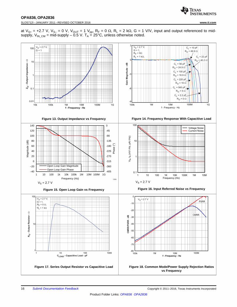
7.6 Electrical Characteristics: VS = 2.7 Vat VS+ = +2.7 V, VS– = 0 V, VOUT = 1 VPP, RF = 0 Ω, RL = 2 kΩ, G = 1 V/V, input and output referenced to mid-supply, VIN_CM =mid-supply – 0.5 V. TA = 25°C, unless otherwise noted.
PARAMETER TEST CONDITIONS MIN TYP MAX UNIT TESTLEVEL (1)
AC PERFORMANCE
Small-signal bandwidth
VOUT = 100 mVPP, G = 1 200
MHz CVOUT = 100 mVPP, G = 2 100
VOUT = 100 mVPP, G = 5 26
VOUT = 100 mVPP, G = 10 11
Gain-bandwidth product VOUT = 100 mVPP, G = 10 110 MHz C
Large-signal bandwidth VOUT = 1 VPP, G = 2 60 MHz C
Bandwidth for 0.1-dB flatness VOUT = 1 VPP, G = 2 25 MHz C
Slew rate, rise VOUT = 1 VSTEP, G = 2 260 V/µs C
Slew rate, fall VOUT = 1 VSTEP, G = 2 240 V/µs C
Rise time VOUT = 1 VSTEP, G = 2 4 ns C
Fall time VOUT = 1 VSTEP, G = 2 4.5 ns C
Settling time to 1%, rise VOUT = 1 VSTEP, G = 2 15 ns C
Settling time to 1%, fall VOUT = 1 VSTEP, G = 2 15 ns C
Settling time to 0.1%, rise VOUT = 1 VSTEP, G = 2 30 ns C
Settling time to 0.1%, fall VOUT = 1 VSTEP, G = 2 25 ns C
Settling time to 0.01%, rise VOUT = 1 VSTEP, G = 2 50 ns C
Settling time to 0.01%, fall VOUT = 1 VSTEP, G = 2 45 ns C
Overshoot/Undershoot VOUT = 1 VSTEP, G = 2 5%/3% C
Second-order harmonic distortion
f = 10 kHz, VIN_CM = mid-supply – 0.5 V –133
dBc
C
f = 100 kHz, VIN_CM = mid-supply – 0.5 V –120 C
f = 1 MHz, VIN_CM = mid-supply – 0.5 V –84 C
Third-order harmonic distortion
f = 10 kHz, VIN_CM = mid-supply – 0.5 V –137
dBc
C
f = 100 kHz, VIN_CM = mid-supply – 0.5 V –130 C
f = 1 MHz, VIN_CM = mid-supply – 0.5 V –105 C
Second-order intermodulation distortionf = 1 MHz, 200-kHz Tone Spacing,VOUT Envelope = 1 VPPVIN_CM = mid-supply – 0.5 V
–90 dBc C
Third-order intermodulation distortionf = 1 MHz, 200-kHz Tone Spacing,VOUT Envelope = 1 VPPVIN_CM = mid-supply – 0.5 V
–90 dBc C
Input voltage noise f = 100 KHz 4.6 nV/√Hz C
Voltage noise 1/f corner frequency 215 Hz C
Input current noise f = 1 MHz 0.75 pA/√Hz C

9
OPA836, OPA2836www.ti.com SLOS712I –JANUARY 2011–REVISED OCTOBER 2016
Product Folder Links: OPA836 OPA2836
Submit Documentation FeedbackCopyright © 2011–2016, Texas Instruments Incorporated
Electrical Characteristics: VS = 2.7 V (continued)at VS+ = +2.7 V, VS– = 0 V, VOUT = 1 VPP, RF = 0 Ω, RL = 2 kΩ, G = 1 V/V, input and output referenced to mid-supply, VIN_CM =mid-supply – 0.5 V. TA = 25°C, unless otherwise noted.
PARAMETER TEST CONDITIONS MIN TYP MAX UNIT TESTLEVEL (1)
(2) Input Offset Voltage Drift, Input Bias Current Drift, and Input Offset Current Drift are average values calculated by taking data at the endpoints, computing the difference, and dividing by the temperature range.
(3) Current is considered positive out of the pin.
AC PERFORMANCE (continued)
Current noise 1/f corner frequency 31.7 kHz C
Overdrive recovery time, over/under Overdrive = 0.5 V 55/60 ns C
Closed-loop output impedance f = 100 kHz 0.02 Ω C
Channel-to-channel crosstalk (OPA2836) f = 10 kHz –120 dB C
DC PERFORMANCE
Open-loop voltage gain (AOL) 100 125 dB A
Input referred offset voltage
TA = 25°C –400 ±65 400
µV
A
TA = 0°C to 70°C –680 680
BTA = –40°C to 85°C –760 760
TA = –40°C to 125°C –1060 1060
Input offset voltage drift (2)
TA = 0°C to 70°C –6.2 ±1 6.2
µV/°C BTA = –40°C to 85°C –6 ±1 6
TA = –40°C to 125°C –6.6 ±1.1 6.6
Input bias current (3)
TA = 25°C 300 650 1000
nA
A
TA = 0°C to 70°C 190 1400
BTA = –40°C to 85°C 120 1500
TA = –40°C to 125°C 120 1800
Input bias current drift (2)
TA = 0°C to 70°C –2 ±0.33 2
nA/°C BTA = –40°C to 85°C –1.9 ±0.32 1.9
TA = –40°C to 125°C –2.1 ±0.37 2.1
Input offset current
TA = 25°C –180 ±30 180
nA
A
TA = 0°C to 70°C –200 ±30 200
BTA = –40°C to 85°C –215 ±30 215
TA = –40°C to 125°C –240 ±30 240
Input offset current drift (2)
TA = 0°C to 70°C –460 ±77 460
pA/°C BTA = –40°C to 85°C –575 ±95 575
TA = –40°C to 125°C –600 ±100 600
INPUT
Common-mode input range low
TA = 25°C,< 3-dB degradation in CMRR limit –0.2 0 V A
TA = –40°C to 125°C,< 3-dB degradation in CMRR limit –0.2 0 V B
Common-mode input range high
TA = 25°C,< 3-dB degradation in CMRR limit 1.5 1.6 V A
TA = –40°C to 125°C,< 3-dB degradation in CMRR limit 1.5 1.6 V B
Input operating voltage range TA = 25°C,< 6-dB degradation in THD
–0.3 to1.75 V C
Common-mode rejection ratio 91 114 dB A
Input impedance common-mode 200 || 1.2 kΩ || pF C
Input impedance differential mode 200 || 1 kΩ || pF C

10
OPA836, OPA2836SLOS712I –JANUARY 2011–REVISED OCTOBER 2016 www.ti.com
Product Folder Links: OPA836 OPA2836
Submit Documentation Feedback Copyright © 2011–2016, Texas Instruments Incorporated
Electrical Characteristics: VS = 2.7 V (continued)at VS+ = +2.7 V, VS– = 0 V, VOUT = 1 VPP, RF = 0 Ω, RL = 2 kΩ, G = 1 V/V, input and output referenced to mid-supply, VIN_CM =mid-supply – 0.5 V. TA = 25°C, unless otherwise noted.
PARAMETER TEST CONDITIONS MIN TYP MAX UNIT TESTLEVEL (1)
OUTPUT
Output voltage lowTA = 25°C, G = 5 0.15 0.2 V A
TA = –40°C to 125°C, G = 5 0.15 0.2 V B
Output voltage highTA = 25°C, G = 5 2.45 2.5 V A
TA = –40°C to 125°C, G = 5 2.45 2.5 V B
Output saturation voltage, high/low TA = 25°C, G = 5 80/40 mV C
Output current driveTA = 25°C ±40 ±45 mA A
TA = –40°C to 125°C ±40 ±45 mA B
GAIN SETTING RESISTORS (OPA836IRUN ONLY)
Resistor FB1 to FB2 DC resistance 1584 1600 1616 Ω A
Resistor FB2 to FB3 DC resistance 1188 1200 1212 Ω A
Resistor FB3 to FB4 DC resistance 396 400 404 Ω A
Resistor tolerance DC resistance –1% 1% A
Resistor temperature coefficient DC resistance <10 PPM C
POWER SUPPLY
Specified operating voltage 2.5 5.5 V B
Quiescent operating current per amplifierTA = 25°C 0.7 0.95 1.15 mA A
TA = –40°C to 125°C 0.6 1.4 mA B
Power supply rejection (±PSRR) 91 108 dB A
POWER DOWN
Enable voltage threshold Specified "on" above VS– + 2.1 V 2.1 V A
Disable voltage threshold Specified "off" below VS– + 0.7 V 0.7 V A
Power-down pin bias current PD = 0.5 V 20 500 nA A
Power-down quiescent current PD = 0. 5 V 0.5 1.5 µA A
Turnon time delay Time from PD = high to VOUT = 90% of finalvalue 200 ns C
Turnoff time delay Time from PD = low to VOUT = 10% of originalvalue 25 ns C
(1) Test levels (all values set by characterization and simulation): (A) 100% tested at 25°C; over temperature limits by characterization andsimulation. (B) Not tested in production; limits set by characterization and simulation. (C) Typical value only for information.
7.7 Electrical Characteristics: VS = 5 Vat VS+ = +5 V, VS– = 0 V, VOUT = 2 VPP, RF = 0 Ω, RL = 1 kΩ, G = 1 V/V, input and output referenced to mid-supply. TA = 25°C,unless otherwise noted.
PARAMETER TEST CONDITIONS MIN TYP MAX UNIT TESTLEVEL (1)
AC PERFORMANCE
Small-signal bandwidth
VOUT = 100 mVPP, G = 1 205
MHz CVOUT = 100 mVPP, G = 2 100
VOUT = 100 mVPP, G = 5 28
VOUT = 100 mVPP, G = 10 11.8
Gain-bandwidth product VOUT = 100 mVPP, G = 10 118 MHz C
Large-signal bandwidth VOUT = 2 VPP, G = 2 87 MHz C
Bandwidth for 0.1-dB flatness VOUT = 2 VPP, G = 2 29 MHz C
Slew rate, rise VOUT = 2-V Step, G = 2 560 V/µs C
Slew rate, fall VOUT = 2-V Step, G = 2 580 V/µs C
Rise time VOUT = 2-V Step, G = 2 3 ns C
Fall time VOUT = 2-V Step, G = 2 3 ns C

11
OPA836, OPA2836www.ti.com SLOS712I –JANUARY 2011–REVISED OCTOBER 2016
Product Folder Links: OPA836 OPA2836
Submit Documentation FeedbackCopyright © 2011–2016, Texas Instruments Incorporated
Electrical Characteristics: VS = 5 V (continued)at VS+ = +5 V, VS– = 0 V, VOUT = 2 VPP, RF = 0 Ω, RL = 1 kΩ, G = 1 V/V, input and output referenced to mid-supply. TA = 25°C,unless otherwise noted.
PARAMETER TEST CONDITIONS MIN TYP MAX UNIT TESTLEVEL (1)
(2) Input Offset Voltage Drift, Input Bias Current Drift, and Input Offset Current Drift are average values calculated by taking data at the endpoints, computing the difference, and dividing by the temperature range.
(3) Current is considered positive out of the pin.
AC PERFORMANCE (continued)
Settling time to 1%, rise VOUT = 2-V Step, G = 2 22 ns C
Settling time to 1%, fall VOUT = 2-V Step, G = 2 22 ns C
Settling time to 0.1%, rise VOUT = 2-V Step, G = 2 30 ns C
Settling time to 0.1%, fall VOUT = 2-V Step, G = 2 30 ns C
Settling time to 0.01%, rise VOUT = 2-V Step, G = 2 40 ns C
Settling time to 0.01%, fall VOUT = 2-V Step, G = 2 45 ns C
Overshoot/Undershoot VOUT = 2-V Step, G = 2 7.5%/5% C
Second-order harmonic distortion
f = 10 kHz –133
dBc Cf = 100 kHz –120
f = 1 MHz –85
Third-order harmonic distortion
f = 10 kHz –140
dBc Cf = 100 kHz –130
f = 1 MHz –105
Second-order intermodulation distortion f = 1 MHz, 200 kHz Tone Spacing,VOUT Envelope = 2 VPP
–79 dBc C
Third-order intermodulation distortion f = 1 MHz, 200 kHz Tone Spacing,VOUT Envelope = 2 VPP
–91 dBc C
Signal-to-noise ratio, SNR f = 1 kHz, VOUT = 1 VRMS,22 kHz bandwidth
0.00013%C
–117.6 dBc
Total harmonic distortion, THD f = 1 kHz, VOUT = 1 VRMS0.00003%
C–130 dBc
Input voltage noise f = 100 KHz 4.6 nV/√Hz C
Voltage noise 1/f corner frequency 215 Hz C
Input current noise f > 1 MHz 0.75 pA/√Hz C
Current noise 1/f corner frequency 31.7 kHz C
Overdrive recovery time, over/under Overdrive = 0.5 V 55/60 ns C
Closed-loop output impedance f = 100 kHz 0.02 Ω C
Channel to channel crosstalk (OPA2836) f = 10 kHz –120 dB C
DC PERFORMANCE
Open-loop voltage gain (AOL) 100 122 dB A
Input referred offset voltage
TA = 25°C –400 ±65 400
µV
A
TA = 0°C to 70°C –685 685
BTA = –40°C to 85°C –765 765
TA = –40°C to 125°C –1080 1080
Input offset voltage drift (2)
TA = 0°C to 70°C –6.3 ±1.05 6.3
µV/°C BTA = –40°C to 85°C –6.1 ±1 6.1
TA = –40°C to 125°C –6.8 ±1.1 6.8
Input bias current (3)
TA = 25°C 300 650 1000
nA
A
TA = 0°C to 70°C 190 1400
BTA = –40°C to 85°C 120 1550
TA = –40°C to 125°C 120 1850
Input bias current drift (2)
TA = 0°C to 70°C ±0.34 ±2
nA/°C BTA = –40°C to 85°C ±0.34 ±2
TA = –40°C to 125°C ±0.38 ±2.3

12
OPA836, OPA2836SLOS712I –JANUARY 2011–REVISED OCTOBER 2016 www.ti.com
Product Folder Links: OPA836 OPA2836
Submit Documentation Feedback Copyright © 2011–2016, Texas Instruments Incorporated
Electrical Characteristics: VS = 5 V (continued)at VS+ = +5 V, VS– = 0 V, VOUT = 2 VPP, RF = 0 Ω, RL = 1 kΩ, G = 1 V/V, input and output referenced to mid-supply. TA = 25°C,unless otherwise noted.
PARAMETER TEST CONDITIONS MIN TYP MAX UNIT TESTLEVEL (1)
DC PERFORMANCE (continued)
Input offset current
TA = 25°C ±30 ±180
nA
A
TA = 0°C to 70°C ±30 ±200
BTA = –40°C to 85°C ±30 ±215
TA = –40°C to 125°C ±30 ±250
Input offset current drift (2)
TA = 0°C to 70°C ±80 ±480
pA/°C BTA = –40°C to 85°C ±100 ±600
TA = –40°C to 125°C ±110 ±660
INPUT
Common-mode input range low
TA = 25°C,< 3-dB degradation in CMRR limit –0.2 0 V A
TA = –40°C to 125°C,< 3-dB degradation in CMRR limit –0.2 0 V B
Common-mode input range high
TA = 25°C,< 3-dB degradation in CMRR limit 3.8 3.9 V A
TA = –40°C to 125°C,< 3-dB degradation in CMRR limit 3.8 3.9 V B
Input linear operating voltage range TA = 25°C,< 6-dB degradation in THD
–0.3 to4.05 V C
Common-mode rejection ratio 94 116 dB A
Input impedance common mode 200 || 1.2 kΩ || pF C
Input impedance differential mode 200 || 1 kΩ || pF C
OUTPUT
Output voltage lowTA = 25°C, G = 5 0.15 0.2 V A
TA = –40°C to 125°C, G = 5 0.15 0.2 V B
Output voltage highTA = 25°C, G = 5 4.75 4.8 V A
TA = –40°C to 125°C, G = 5 4.75 4.8 V B
Output saturation voltage, high/low TA = 25°C, G = 5 100/50 mV C
Output current driveTA = 25°C ±40 ±50 mA A
TA = –40°C to 125°C ±40 ±50 mA B
GAIN SETTING RESISTORS (OPA836IRUN ONLY)
Resistor FB1 to FB2 DC resistance 1584 1600 1616 Ω A
Resistor FB2 to FB3 DC resistance 1188 1200 1212 Ω A
Resistor FB3 to FB4 DC resistance 396 400 404 Ω A
Resistor tolerance DC resistance –1 1% A
Resistor temperature coefficient DC resistance <10 PPM C
POWER SUPPLY
Specified operating voltage 2.5 5.5 V B
Quiescent operating current per amplifierTA = 25°C 0.8 1.0 1.2 mA A
TA = –40°C to 125°C 0.65 1.5 mA B
Power supply rejection (±PSRR) 94 108 dB A
POWER DOWN
Enable voltage threshold Specified "on" above VS–+ 2.1 V 2.1 V A
Disable voltage threshold Specified "off" below VS–+ 0.7 V 0.7 V A
Power-down pin bias current PD = 0.5 V 20 500 nA A
Power-down quiescent current PD = 0.5 V 0.5 1.5 µA A
Turnon time delay Time from PD = high to VOUT = 90%of final value 170 ns C
Turnoff time delay Time from PD = low to VOUT = 10% oforiginal value 35 ns C

13
OPA836, OPA2836www.ti.com SLOS712I –JANUARY 2011–REVISED OCTOBER 2016
Product Folder Links: OPA836 OPA2836
Submit Documentation FeedbackCopyright © 2011–2016, Texas Instruments Incorporated
7.8 Typical Characteristics
7.8.1 Typical Characteristics: VS = 2.7 VTable 1. Table of Graphs
FIGURE TITLE FIGURE LOCATIONSmall Signal Frequency Response Figure 1Large Signal Frequency Response Figure 2Noninverting Pulse Response Figure 3Inverting Pulse Response Figure 4Slew Rate vs Output Voltage Step Figure 5Output Overdrive Recovery Figure 6Harmonic Distortion vs Frequency Figure 7Harmonic Distortion vs Load Resistance Figure 8Harmonic Distortion vs Output Voltage Figure 9Harmonic Distortion vs Gain Figure 10Output Voltage Swing vs Load Resistance Figure 11Output Saturation Voltage vs Load Current Figure 12Output Impedance vs Frequency Figure 13Frequency Response With Capacitive Load Figure 14Series Output Resistor vs Capacitive Load Figure 17Input Referred Noise vs Frequency Figure 16Open Loop Gain vs Frequency Figure 15Common Mode/Power Supply Rejection Ratios vs Frequency Figure 18Crosstalk vs Frequency Figure 19Power Down Response Figure 20Input Offset Voltage Figure 23Input Offset Voltage vs Free-Air Temperature Figure 21Input Offset Voltage Drift Figure 48Input Offset Current Figure 24Input Offset Current vs Free-Air Temperature Figure 25Input Offset Current Drift Figure 26
-0.25
0
0.25
0.5
0.75
0 500 1000 1500 2000
t - Time - ns
-1.25
-0.75
-0.25
0.25
0.75
1.25
1.75
2.25
2.75
3.25
3.75
V-
Inp
ut
Vo
lta
ge
- V
I
V-
Ou
tpu
t V
olt
ag
e -
VO
V = 2.7 V,
G = 5,
R = 1 k ,
R = 1 k
S
F
L
W
W
VIN
VOUT
0
50
100
150
200
250
300
0.5 0.6 0.7 0.8 0.9 1
Output Voltage Step -V
Rising
Falling
Sle
w R
ate
- V
/s
m
V = 2.7 V,
G = 2,
R = 1 k
R = 1 k
S
F
L
W
W
0 500 1000t - Time - ns
0
0.5
1
1.5
2
2.5
V-
Ou
tpu
t V
olt
ag
e -
VO
V = 1.5 VppOUT
V = 0.5 VppOUT
V = 2.7 V,
G = 1,
R = 0
R = 1 k
S
F
L
W
W
0
0.5
1
1.5
2
2.5
3
0 500 1000t - Time - ns
V-
Ou
tpu
t V
olt
ag
e -
VO
V = 2.7 V,
G = -1,
R = 1 k
R = 1 k
S
F
L
W
W
V = 2 VppOUT
V = 0.5 VppOUT
100k 1M 10M 100M 1G
f - Frequency - Hz
G = 1
G = 10
G = 5
G = 2
G = -1
-9
-6
-3
0
3
6
9
12
15
18
21
Gain
Mag
nit
ud
e -
dB
V = 2.7 V,
V = 100 mVpp,
R = 1 k
S
OUT
L W
-9
-6
-3
0
3
6
9
12
15
18
21
Ga
in M
ag
nit
ud
e -
dB
100k 1M 10M 100M 1G
f - Frequency - Hz
G = 10
G = 5
G = 2
G = 1
G = -1
V = 2.7 V,
V = 1 Vpp,
R = 1 k
S
OUT
L W
14
OPA836, OPA2836SLOS712I –JANUARY 2011–REVISED OCTOBER 2016 www.ti.com
Product Folder Links: OPA836 OPA2836
Submit Documentation Feedback Copyright © 2011–2016, Texas Instruments Incorporated
at VS+ = +2.7 V, VS– = 0 V, VOUT = 1 Vpp, RF = 0 Ω, RL = 2 kΩ, G = 1 V/V, input and output referenced to mid-supply, VIN_CM = mid-supply – 0.5 V. TA = 25°C, unless otherwise noted.
Figure 1. Small Signal Frequency Response Figure 2. Large Signal Frequency Response
Figure 3. Noninverting Pulse Response Figure 4. Inverting Pulse Response
Figure 5. Slew Rate vs Output Voltage Step Figure 6. Output Overdrive Recovery

0
0.5
1
1.5
2
2.5
3
V-
Ou
tpu
t V
olt
ag
e -
VO
10 100 1k 10k
R - Load Resistance -L W
V = HighOUT
V = LowOUT
V = 2.7 V,
G = 5,
R = 1 k
S
F W
0.001
0.01
0.1
1
0.1 10 100
V = LowOUT
V = HighOUT
V = 2.7 V,
G = 5,
R = 1 k
S
F W
V-
Satu
rati
on
Vo
ltag
e -
VS
AT
1
I - Load Current - mAL
-110
-100
-90
-80
-70
-60
-50
-40
-30
Ha
rmo
nic
Dis
tort
ion
- d
Bc
0 1 2
V - Output Voltage - VppO
HD3
HD2
V = 2.7 V,
G = 1,
f = 1 MHz,
R = 0 ,
R = 1 k
S
F
L
W
W
-110
-105
-100
-95
-90
-85
-80
-75
-70
-65
-60H
arm
on
ic D
isto
rti
on
- d
Bc
1 2 3 4 5 6 7 8 9 10Gain - V/V
V = 2.7 V,
G = 1,f = 1 MHz,V = 1 Vpp,
R = 1 k
S
OUT
L W
HD3
HD2
-110
-105
-100
-95
-90
-85
-80
-75
-70
Ha
rm
on
ic D
isto
rti
on
- d
Bc
100 1k 10k
R - Load Resistance -LOAD
W
V = 2.7 V,
G = 1,f = 1 MHz,
R = 0
V = 1 Vpp
S
F
OUT
W
HD3
HD2
-140
-130
-120
-110
-100
-90
-80
-70
-60
-50
-40
10k 100k 1M 10M
Ha
rmo
nic
Dis
tort
ion
- d
Bc
f - Frequency - Hz
V = 2.7 V,
G = 1,V = 1 Vpp,
R = 0 ,
R = 1 k
S
OUT
F
L
W
W
HD3
HD2
15
OPA836, OPA2836www.ti.com SLOS712I –JANUARY 2011–REVISED OCTOBER 2016
Product Folder Links: OPA836 OPA2836
Submit Documentation FeedbackCopyright © 2011–2016, Texas Instruments Incorporated
at VS+ = +2.7 V, VS– = 0 V, VOUT = 1 Vpp, RF = 0 Ω, RL = 2 kΩ, G = 1 V/V, input and output referenced to mid-supply, VIN_CM = mid-supply – 0.5 V. TA = 25°C, unless otherwise noted.
Figure 7. Harmonic Distortion vs Frequency Figure 8. Harmonic Distortion vs Load Resistance
Figure 9. Harmonic Distortion vs Output Voltage Figure 10. Harmonic Distortion vs Gain
Figure 11. Output Voltage Swing vs Load Resistance Figure 12. Output Saturation Voltage vs Load Current
1
10
100
R-
Ou
tpu
t R
es
isto
r -
OW
1 10 100 1000
C - Capacitive Load - pFLOAD
V = 2.7 V,
G = 1,
R = 0 ,
R = 1 k
S
F
L
W
W
100k 1M 10M 100M
PSRR
CMRR
-80
-70
-60
-50
-40
-30
-20
-10
0
CM
RR
/PS
RR
- d
B
f - Frequency - Hz
V = 2.7 VS
1 10 100 1k 10k 100k 1M 10M 100M 1G -405
-360
-315
-270
-225
-180
-135
-90
-45
0
±40
±20
0
20
40
60
80
100
120
140
Pha
se ()
Mag
nitu
de (
dB)
Frequency (Hz)
Open Loop Gain Magnitude
Open Loop Gain Phase
C001 Frequency (Hz)
VN, I N
(nV
/√H
z,
pA
/√H
z)
1 10 100 1K 10K 100K 1M 10M0.1
1
10
100Voltage NoiseCurrent Noise
0.01
0.1
1
10
100
10k 100k 1M 10M 100M 1G
f - Frequency - Hz
Z-
Ou
tpu
t Im
pe
da
nc
e -
OW
V = 2.7 V,
G = 1S
-9
-6
-3
0
3
100k 1M 10M 100M 1G
f - Frequency - Hz
Ga
in M
ag
nit
ud
e -
dB
V = 2.7 V,
G = 1,
R = 0
R = 1 k
S
F
L
W
W,
C = 56 pF
R = 24.9
L
O W
C = 100 pF
R = 16.9
L
O W
C = 220 pF
R = 10
L
O W
C = 560 pF
R = 5
L
O W
C = 2.2 pF
R = 0
L
O W
C = 10 pF
R = 49.9
L
O W
C = 22 pF
R = 40.2
L
O W
16
OPA836, OPA2836SLOS712I –JANUARY 2011–REVISED OCTOBER 2016 www.ti.com
Product Folder Links: OPA836 OPA2836
Submit Documentation Feedback Copyright © 2011–2016, Texas Instruments Incorporated
at VS+ = +2.7 V, VS– = 0 V, VOUT = 1 Vpp, RF = 0 Ω, RL = 2 kΩ, G = 1 V/V, input and output referenced to mid-supply, VIN_CM = mid-supply – 0.5 V. TA = 25°C, unless otherwise noted.
Figure 13. Output Impedance vs Frequency Figure 14. Frequency Response With Capacitive Load
VS = 2.7 V
Figure 15. Open Loop Gain vs Frequency
VS = 2.7 V
Figure 16. Input Referred Noise vs Frequency
Figure 17. Series Output Resistor vs Capacitive Load Figure 18. Common Mode/Power Supply Rejection Ratiosvs Frequency
0 0 0 0 0 0 7 30
207
1268
2666
1507
311
34 3 2 0 0 0 0 0 00
500
1000
1500
2000
2500
3000
Co
un
t
<-6
94
.3
<-6
24
.87
<-5
55
.44
<-4
86
.01
<-4
16
.58
<-3
47
.15
<-2
77
.72
<-2
08
.29
<-1
38
.86
<-6
9.4
3
<0
<6
9.4
3
<1
38
.86
<2
08
.29
<2
77
.72
<3
47
.15
<4
16
.58
<4
86
.01
<5
55
.44
<6
24
.87
<6
94
.3
>6
94
.3
I - Offset Current - nAOS
20 8 7 11 15 28 40 80
233
768
1532
1687
964
365
12558
29 29 9 10 4 13
0
200
400
600
800
1000
1200
1400
1600
1800
Co
un
t
I - Offset Current - nAOS
<-1
36
.6
<-1
22
.94
<-1
09
.28
<-9
5.6
2
<-8
1.9
6
<-6
8.3
<-5
4.6
4
<-4
0.9
8
<-2
7.3
2
<-1
3.6
6
<-0
<1
3.6
6
<2
7.3
2
<4
0.9
8
<5
4.6
4
<6
8.3
<8
1.9
6
<9
5.6
2
<1
09
.28
<1
22
.94
<1
36
.6
>3
6.6
-400
-300
-200
-100
0
100
200
300
400
V-
Off
set
Vo
ltag
e -
VO
Sm
-40 -20 0 20 40 60 80 100 120
T - Free-Air Temperature - °CA
0
1
2
3
4
5
6
7
8
-5 -4.5 -4 -3.5 -3-2.5 -2 -1.5 -1 -0.5 0 0.5 1 1.5 2 2.5 3 3.5 4 4.5 5
V - Drift - V/°COS
m
Co
un
t0°C to 70°C
-40°C to 85°C
-40°C to 125°C
−140
−130
−120
−110
−100
−90
−80
20 100 1k 10k 100k 1M 10M 100M
Frequency (Hz)
Cro
ssta
lk (
dB
)
0
0.5
1
1.5
2
2.5
3
0 500 1000
t - Time - ns
VPD
VOUT
V = 2.7 V,
G = 2,
R = 1 k
R = 1 k
S
F
L
W,
W
VO
UT
PD
/V
17
OPA836, OPA2836www.ti.com SLOS712I –JANUARY 2011–REVISED OCTOBER 2016
Product Folder Links: OPA836 OPA2836
Submit Documentation FeedbackCopyright © 2011–2016, Texas Instruments Incorporated
at VS+ = +2.7 V, VS– = 0 V, VOUT = 1 Vpp, RF = 0 Ω, RL = 2 kΩ, G = 1 V/V, input and output referenced to mid-supply, VIN_CM = mid-supply – 0.5 V. TA = 25°C, unless otherwise noted.
Figure 19. Crosstalk vs Frequency Figure 20. Power Down Response
Figure 21. Input Offset Voltage vs Free-Air Temperature Figure 22. Input Offset Voltage Drift
Figure 23. Input Offset Voltage Figure 24. Input Offset Current

-150
-100
-50
0
50
100
150
I-
Off
set
Cu
rren
t -
nA
OS
-40 -20 0 20 40 60 80 100 120
T - Free-Air Temperature - °CA
0
2
4
6
8
10
12
14
-400-350-300-250-200-150-100 -50 0 50 100 150 200 250 300 350 400
I - Drift - pA/°COS
Co
un
t
0°C to 70°C
-40°C to 85°C
-40°C to 125°C
18
OPA836, OPA2836SLOS712I –JANUARY 2011–REVISED OCTOBER 2016 www.ti.com
Product Folder Links: OPA836 OPA2836
Submit Documentation Feedback Copyright © 2011–2016, Texas Instruments Incorporated
at VS+ = +2.7 V, VS– = 0 V, VOUT = 1 Vpp, RF = 0 Ω, RL = 2 kΩ, G = 1 V/V, input and output referenced to mid-supply, VIN_CM = mid-supply – 0.5 V. TA = 25°C, unless otherwise noted.
Figure 25. Input Offset Current vs Free-Air Temperature Figure 26. Input Offset Current Drift

19
OPA836, OPA2836www.ti.com SLOS712I –JANUARY 2011–REVISED OCTOBER 2016
Product Folder Links: OPA836 OPA2836
Submit Documentation FeedbackCopyright © 2011–2016, Texas Instruments Incorporated
7.8.2 Typical Performance Graphs: VS = 5 V
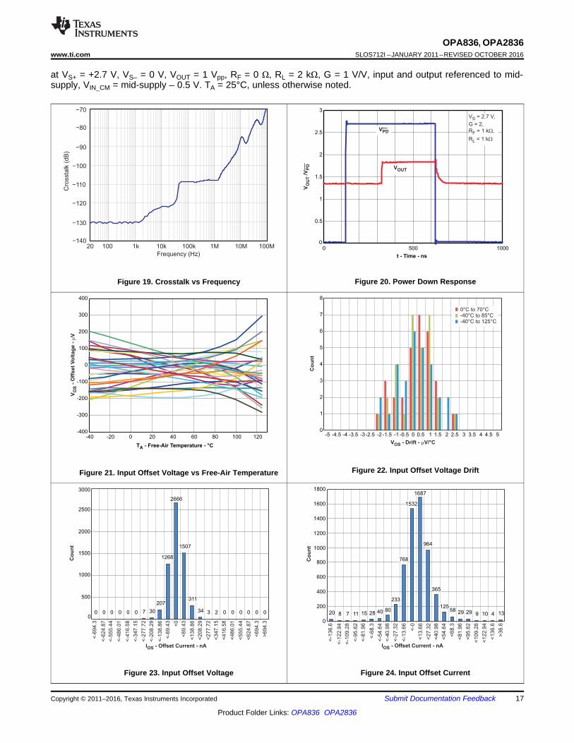
Table 2. Table of GraphsFIGURE TITLE FIGURE LOCATION
Small Signal Frequency Response Figure 27Large Signal Frequency Response Figure 28Noninverting Pulse Response Figure 29Inverting Pulse Response Figure 30Slew Rate vs Output Voltage Step Figure 31Output Overdrive Recovery Figure 32Harmonic Distortion vs Frequency Figure 33Harmonic Distortion vs Load Resistance Figure 34Harmonic Distortion vs Output Voltage Figure 35Harmonic Distortion vs Gain Figure 36Output Voltage Swing vs Load Resistance Figure 37Output Saturation Voltage vs Load Current Figure 38Output Impedance vs Frequency Figure 39Frequency Response With Capacitive Load Figure 40Series Output Resistor vs Capacitive Load Figure 43Input Referred Noise vs Frequency Figure 41Open Loop Gain vs Frequency Figure 42Common Mode/Power Supply Rejection Ratios vs Frequency Figure 44Crosstalk vs Frequency Figure 45Power Down Response Figure 46Input Offset Voltage Figure 49Input Offset Voltage vs Free-Air Temperature Figure 47Input Offset Voltage Drift Figure 48Input Offset Current Figure 50Input Offset Current vs Free-Air Temperature Figure 51Input Offset Current Drift Figure 52
-0.25
0
0.25
0.5
0.75
1
1.25
-1.25
-0.75
-0.25
0.25
0.75
1.25
1.75
2.25
2.75
3.25
3.75
4.25
4.75
5.25
5.75
6.25
0 500 1000 1500 2000
t - Time - ns
V-
Inp
ut
Vo
ltag
e -
VI
V-
Ou
tpu
t V
olt
ag
e -
VO
V = 5 V,
G = 5,
R = 1 k ,
R = 1 k
S
F
L
W
W
VIN
VOUT
0
100
200
300
400
500
600
700
0 1 2 3 4
Rising
Falling
Sle
w R
ate
- V
/s
m
Output Voltage Step -V
V = 5 V,
G = 2,
R = 1 k
R = 1 k
S
F
L
W
W
0
0.5
1
1.5
2
2.5
3
3.5
4
4.5
5
V-
Ou
tpu
t V
olt
ag
e -
VO
0 500 1000
t - Time - ns
V = 4 VppOUT
V = 0.5 VppOUT
V = 5 V,
G = 1,
R = 1 k
R = 1 k
S
F
L
W
W
0
0.5
1
1.5
2
2.5
3
3.5
4
4.5
5
V-
Ou
tpu
t V
olt
ag
e -
VO
0 500 1000t - Time - ns
V = 5 V,
G = 1,
R = 0
R = 1 k
S
F
L
W
W
V = 4 VppOUT
V = 0.5 VppOUT
-9
-6
-3
0
3
6
9
12
15
18
21
Ga
in M
ag
nit
ud
e -
dB
100k 1M 10M 100M 1G
f - Frequency - Hz
G = 10
G = 5
G = 2
G = 1
G = -1
V = 5 V,
V = 2 Vpp,
R = 1 k
S
OUT
L W
-9
-6
-3
0
3
6
9
12
15
18
21
Ga
in M
ag
nit
ud
e -
dB
100k 1M 10M 100M 1G
f - Frequency - Hz
G = 10
G = 5
G = 2
G = 1
G = -1
V = 5 V,
V = 100 mVpp,
R = 1 k
S
OUT
L W
20
OPA836, OPA2836SLOS712I –JANUARY 2011–REVISED OCTOBER 2016 www.ti.com
Product Folder Links: OPA836 OPA2836
Submit Documentation Feedback Copyright © 2011–2016, Texas Instruments Incorporated
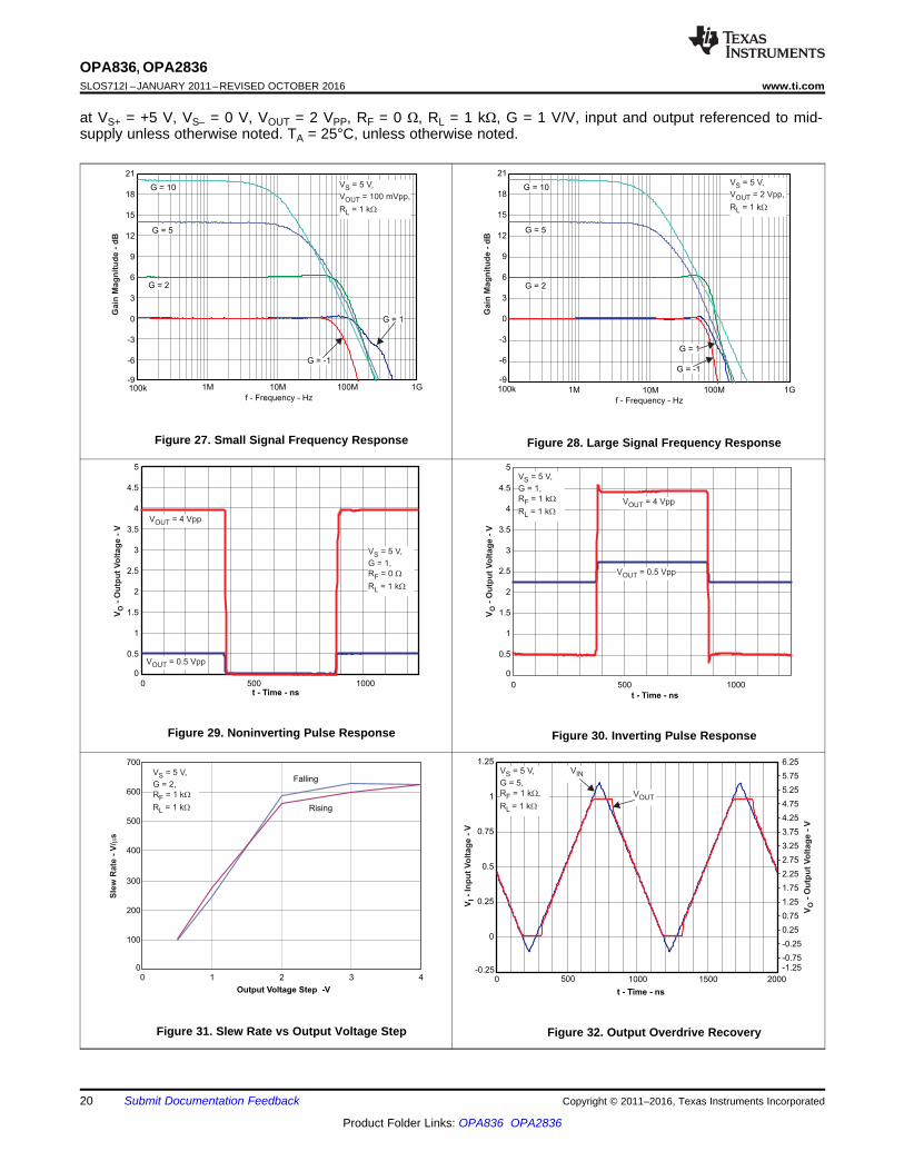
at VS+ = +5 V, VS– = 0 V, VOUT = 2 VPP, RF = 0 Ω, RL = 1 kΩ, G = 1 V/V, input and output referenced to mid-supply unless otherwise noted. TA = 25°C, unless otherwise noted.
Figure 27. Small Signal Frequency Response Figure 28. Large Signal Frequency Response
Figure 29. Noninverting Pulse Response Figure 30. Inverting Pulse Response
Figure 31. Slew Rate vs Output Voltage Step Figure 32. Output Overdrive Recovery
0.01
0.1
1
V-
Satu
rati
on
Vo
ltag
e -
VS
AT
0.1 10 1001
I - Load Current - mAL
V = LowOUT
V = HighOUT
V = 5 V,
G = 5,
R = 1 k
S
F W
0
1
2
3
4
5
V-
Ou
tpu
t V
olt
ag
e -
VO
10 100 1k 10k
R - Load Resistance -L W
V = LowOUT
V = HighOUT
V = 5 V,
G = 2,
R = 1 k
S
F W
-110
-105
-100
-95
-90
-85
-80
-75
-70
-65
-60H
arm
on
ic D
isto
rti
on
- d
Bc
1 2 3 4 5 6 7 8 9 10Gain - V/V
V = 5 V,
G = 1,f = 1 MHz,V = 2 Vpp,
R = 1 k
S
OUT
L W
HD3
HD2
-110
-105
-100
-95
-90
-85
-80
-75
-70
0 1 2 3 4
Ha
rmo
nic
Dis
tort
ion
- d
Bc
V - Output Voltage - VppO
HD3
HD2
V = 5 V,
G = 1,
f = 1 MHz,
R = 0 ,
R = 1 k
S
F
L
W
W
-110
-105
-100
-95
-90
-85
-80
-75
-70
Ha
rm
on
ic D
isto
rti
on
- d
Bc
100 1k 10k
R - Load Resistance -LOAD
W
HD3
HD2
V = 5 V,
G = 1,f = 1 MHz,
R = 0
V = 2 Vpp
S
F
OUT
W
-140
-130
-120
-110
-100
-90
-80
-70
-60
-50
-40
10k 100k 1M 10M
Ha
rmo
nic
Dis
tort
ion
- d
Bc
f - Frequency - Hz
HD3
HD2
V = 5 V,
G = 1,V = 2 Vpp,
R = 0 ,
R = 1 k
S
OUT
F
L
W
W
21
OPA836, OPA2836www.ti.com SLOS712I –JANUARY 2011–REVISED OCTOBER 2016
Product Folder Links: OPA836 OPA2836
Submit Documentation FeedbackCopyright © 2011–2016, Texas Instruments Incorporated
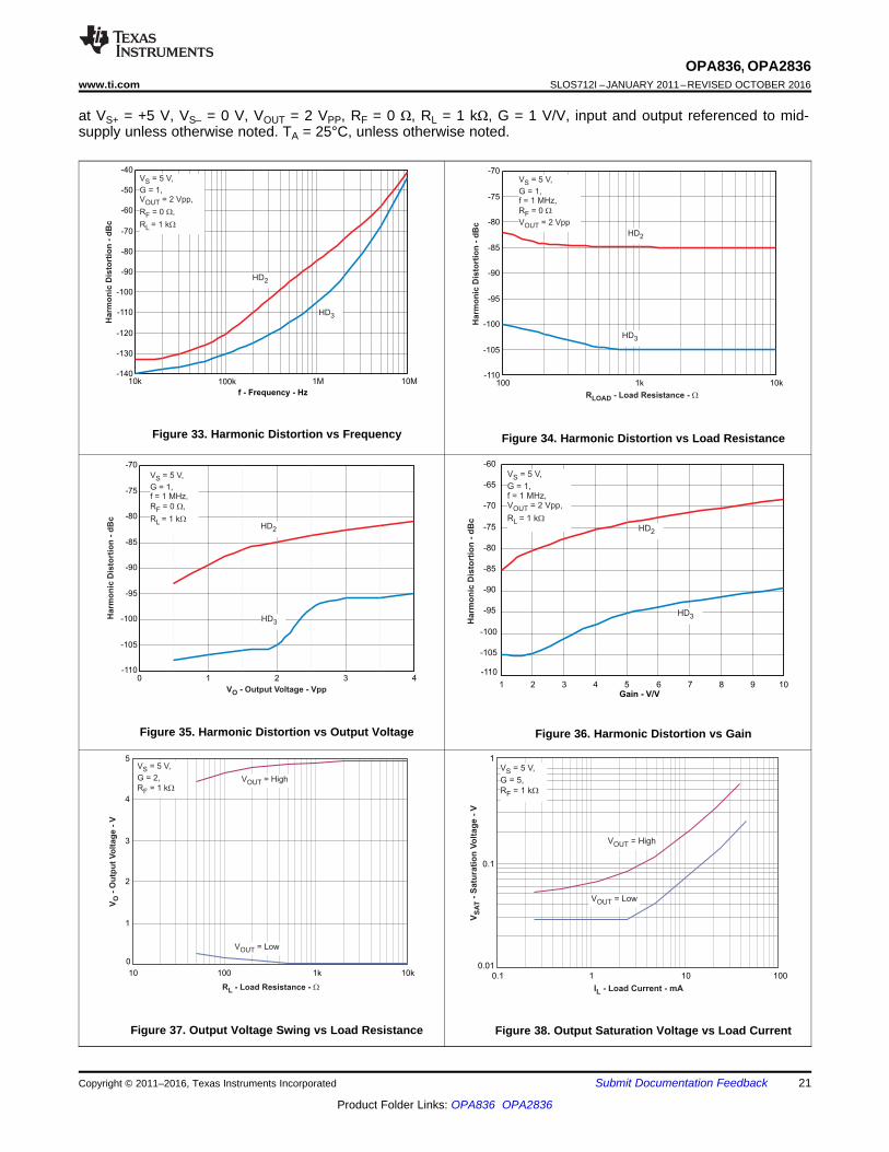
at VS+ = +5 V, VS– = 0 V, VOUT = 2 VPP, RF = 0 Ω, RL = 1 kΩ, G = 1 V/V, input and output referenced to mid-supply unless otherwise noted. TA = 25°C, unless otherwise noted.
Figure 33. Harmonic Distortion vs Frequency Figure 34. Harmonic Distortion vs Load Resistance
Figure 35. Harmonic Distortion vs Output Voltage Figure 36. Harmonic Distortion vs Gain
Figure 37. Output Voltage Swing vs Load Resistance Figure 38. Output Saturation Voltage vs Load Current
100k 1M 10M 100M
PSRR
CMRR
-80
-70
-60
-50
-40
-30
-20
-10
0
CM
RR
/PS
RR
- d
B
f - Frequency - Hz
V = 5 VS
1
10
100
R-
Ou
tpu
t R
es
isto
r -
OW
1 10 100 1000
C - Capacitive Load - pFLOAD
V = 5 V,
G = 1,
R = 0 ,
R = 1 k
S
F
L
W
W
1 10 100 1k 10k 100k 1M 10M 100M 1G -405
-360
-315
-270
-225
-180
-135
-90
-45
0
±40
±20
0
20
40
60
80
100
120
140
Pha
se ()
Mag
nitu
de (
dB)
Frequency (Hz)
Open Loop Gain Magnitude
Open Loop Gain Phase
C002 Frequency (Hz)
VN,
I N(n
V/√
Hz,
pA
/√H
z)
0.1
1
10
100Voltage NoiseCurrent Noise
1 10 100 1K 10K 100K 1M 10M
0.01 0.1 1 10 100 1000
f - Frequency - MHz
0.01
0.1
1
10
100
Z-
Ou
tpu
t Im
pe
da
nc
e -
OW
V = 5 V,
G = 1S
-9
-6
-3
0
3
Ga
in M
ag
nit
ud
e -
dB
100k 1M 10M 100M 1G
f - Frequency - Hz
C = 56 pF
R = 24.9
L
O W
C = 100 pF
R = 16.9
L
O W
C = 220 pF
R = 10
L
O W
C = 560 pF
R = 5
L
O W
C = 2.2 pF
R = 0
L
O W
C = 10 pF
R = 49.9
L
O W
C = 22 pF
R = 40.2
L
O W
V = 5 V,
G = 1,
R = 0
R = 1 k
S
F
L
W
W
22
OPA836, OPA2836SLOS712I –JANUARY 2011–REVISED OCTOBER 2016 www.ti.com
Product Folder Links: OPA836 OPA2836
Submit Documentation Feedback Copyright © 2011–2016, Texas Instruments Incorporated
at VS+ = +5 V, VS– = 0 V, VOUT = 2 VPP, RF = 0 Ω, RL = 1 kΩ, G = 1 V/V, input and output referenced to mid-supply unless otherwise noted. TA = 25°C, unless otherwise noted.
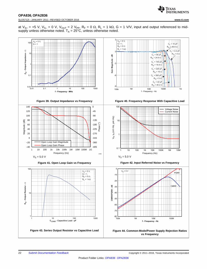
Figure 39. Output Impedance vs Frequency Figure 40. Frequency Response With Capacitive Load
VS = 5.0 V
Figure 41. Open Loop Gain vs Frequency
VS = 5.0 V
Figure 42. Input Referred Noise vs Frequency
Figure 43. Series Output Resistor vs Capacitive Load Figure 44. Common-Mode/Power Supply Rejection Ratiosvs Frequency
0 0 0 0 0 0 7 25
193
1269
2707
1511
289
31 1 2 0 0 0 0 0 0
0
500
1000
1500
2000
2500
3000
Co
un
t
<-6
93
<-6
23
.7
<-5
54
.4
<-4
85
.1
<-4
15
.8
<-3
46
.5
<-2
77
.2
<-2
07
.9
<-1
38
.6
<-6
9.3 <0
<6
9.3
<1
38
.6
<2
07
.9
<2
77
.2
<3
46
.5
<4
15
.8
<4
85
.1
<5
54
.4
<6
23
.7
<6
93
>6
93
V - Offset Voltage - VOS m
20 8 8 9 14 32 43 89
261
788
1525
1641
947
369
12958
28 30 10 8 5 13
<-1
36.5
<-1
22.8
5
<-1
09.2
<-9
5.5
5
<-8
1.9
<-6
8.2
5
<-5
4.6
<-4
0.9
5
<-2
7.3
<-1
3.6
5
<0
<13.6
5
<27.3
<40.9
5
<54.6
<68.2
5
<81.9
<95.5
5
<109.2
<122.8
5
<136.5
>136.5
I - Offset Current - nAOS
0
200
400
600
800
1000
1200
1400
1600
1800
Co
un
t
0
1
2
3
4
5
6
7
8
9
-5 -4.5 -4 -3.5 -3-2.5 -2 -1.5 -1 -0.5 0 0.5 1 1.5 2 2.5 3 3.5 4 4.5 5
V - Drift - V/°COS
m
0°C to 70°C
-40°C to 85°C
-40°C to 125°C
Co
un
t
-400
-300
-200
-100
0
100
200
300
400
V-
Off
se
t V
olt
ag
e -
VO
Sm
-40 -20 0 20 40 60 80 100 120
T - Free-Air Temperature - °CA
0
0.5
1
1.5
2
2.5
3
3.5
4
4.5
5
V/V
OU
TP
D
0 500 1000
t - Time - ns
V = 5 V,
G = 2,
R = 1 k
R = 1 k
S
F
L
W
W
VPD
VOUT
−140
−130
−120
−110
−100
−90
−80
20 100 1k 10k 100k 1M 10M 100M
Frequency (Hz)
Cro
ssta
lk (
dB
)
23
OPA836, OPA2836www.ti.com SLOS712I –JANUARY 2011–REVISED OCTOBER 2016
Product Folder Links: OPA836 OPA2836
Submit Documentation FeedbackCopyright © 2011–2016, Texas Instruments Incorporated
at VS+ = +5 V, VS– = 0 V, VOUT = 2 VPP, RF = 0 Ω, RL = 1 kΩ, G = 1 V/V, input and output referenced to mid-supply unless otherwise noted. TA = 25°C, unless otherwise noted.
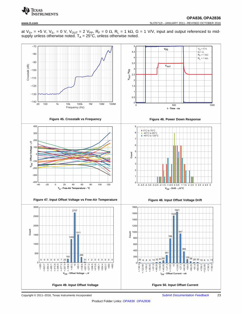
Figure 45. Crosstalk vs Frequency Figure 46. Power Down Response
Figure 47. Input Offset Voltage vs Free-Air Temperature Figure 48. Input Offset Voltage Drift
Figure 49. Input Offset Voltage Figure 50. Input Offset Current
-40 -20 0 20 40 60 80 100 120
T - Free-Air Temperature - °CA
-150
-100
-50
0
50
100
150
I-
Off
set
Cu
rren
t -
nA
OS
0
2
4
6
8
10
12
-400-350-300-250-200-150-100 -50 0 50 100 150 200 250 300 350 400
0°C to 70°C
-40°C to 85°C
-40°C to 125°C
I - Drift - pA/°COS
Co
un
t
24
OPA836, OPA2836SLOS712I –JANUARY 2011–REVISED OCTOBER 2016 www.ti.com
Product Folder Links: OPA836 OPA2836
Submit Documentation Feedback Copyright © 2011–2016, Texas Instruments Incorporated
at VS+ = +5 V, VS– = 0 V, VOUT = 2 VPP, RF = 0 Ω, RL = 1 kΩ, G = 1 V/V, input and output referenced to mid-supply unless otherwise noted. TA = 25°C, unless otherwise noted.
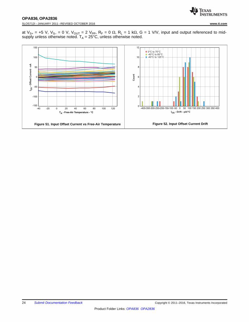
Figure 51. Input Offset Current vs Free-Air Temperature Figure 52. Input Offset Current Drift

RGVIN
OPA836
VSIG
VREF
VREF
VS+
VS-
RF
VOUT
GVSIG
VREF
OPA836
VSIG
VREF
VIN
VREF
RG
VS+
VS-
RF
VOUT
VREF
GVSIG
25
OPA836, OPA2836www.ti.com SLOS712I –JANUARY 2011–REVISED OCTOBER 2016
Product Folder Links: OPA836 OPA2836
Submit Documentation FeedbackCopyright © 2011–2016, Texas Instruments Incorporated
8 Detailed Description
8.1 OverviewThe OPAx836 family of bipolar-input operational amplifiers offers excellent bandwidth of 205 MHz with ultra-lowTHD of 0.00003% at 1 kHz. The OPAx836 device can swing to within 200 mV of the supply rails while driving a1-kΩ load. The input common-mode of the amplifier can swing to 200 mV below the negative supply rail. Thislevel of performance is achieved at 1 mA of quiescent current per amplifier channel.
8.2 Functional Block Diagrams
Figure 53. Noninverting Amplifier
Figure 54. Inverting Amplifier
8.3 Feature Description
8.3.1 Input Common-Mode Voltage RangeWhen the primary design goal is a linear amplifier with high CMRR, it is important to not violate the inputcommon-mode voltage range (VICR) of an operational amplifier.
The common-mode input range specifications in the table data use CMRR to set the limit. The limits are selectedto ensure CMRR will not degrade more than 3 dB below the CMRR limit if the input voltage is kept within thespecified range. The limits cover all process variations and most parts will be better than specified. The typicalspecifications are from 0.2 V below the negative rail to 1.1 V below the positive rail.
Assuming the operational amplifier is in linear operation, the voltage difference between the input pins is small(ideally 0 V) and input common-mode voltage is analyzed at either input pin with the other input pin assumed tobe at the same potential. The voltage at VIN+ is simple to evaluate. In noninverting configuration, Figure 53, theinput signal, VIN, must not violate the VICR. In inverting configuration, Figure 54, the reference voltage, VREF, mustbe within the VICR.
The input voltage limits have fixed headroom to the power rails and track the power supply voltages. For one 5-Vsupply, the linear input voltage ranges from –0.2 V to 3.9 V and from –0.2 V to 1.6 V for a 2.7-V supply. Thedelta headroom from each power supply rail is the same in either case: –0.2 V and 1.1 V.
26
OPA836, OPA2836SLOS712I –JANUARY 2011–REVISED OCTOBER 2016 www.ti.com
Product Folder Links: OPA836 OPA2836
Submit Documentation Feedback Copyright © 2011–2016, Texas Instruments Incorporated
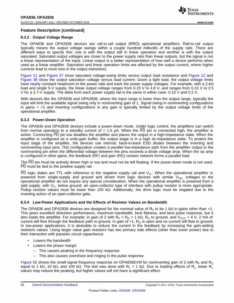
Feature Description (continued)8.3.2 Output Voltage RangeThe OPA836 and OPA2836 devices are rail-to-rail output (RRO) operational amplifiers. Rail-to-rail outputtypically means the output voltage swings within a couple hundred millivolts of the supply rails. There aredifferent ways to specify this: one is with the output still in linear operation and another is with the outputsaturated. Saturated output voltages are closer to the power supply rails than linear outputs, but the signal is nota linear representation of the input. Linear output is a better representation of how well a device performs whenused as a linear amplifier. Saturation and linear operation limits are affected by the output current, where highercurrents lead to more loss in the output transistors.
Figure 11 and Figure 37 show saturated voltage-swing limits versus output load resistance and Figure 12 andFigure 38 show the output saturation voltage versus load current. Given a light load, the output voltage limitshave nearly constant headroom to the power rails and track the power supply voltages. For example, with a 2-kΩload and single 5-V supply, the linear output voltage ranges from 0.15 V to 4.8 V, and ranges from 0.15 V to 2.5V for a 2.7-V supply. The delta from each power supply rail is the same in either case: 0.15 V and 0.2 V.
With devices like the OPA836 and OPA2836, where the input range is lower than the output range, typically theinput will limit the available signal swing only in noninverting gain of 1. Signal swing in noninverting configurationsin gains > +1 and inverting configurations in any gain is typically limited by the output voltage limits of theoperational amplifier.
8.3.3 Power-Down OperationThe OPA836 and OPA2836 devices include a power-down mode. Under logic control, the amplifiers can switchfrom normal operation to a standby current of < 1.5 µA. When the PD pin is connected high, the amplifier isactive. Connecting PD pin low disables the amplifier and places the output in a high-impedance state. When theamplifier is configured as a unity-gain buffer, the output stage is in a high dc-impedance state. To protect theinput stage of the amplifier, the devices use internal, back-to-back ESD diodes between the inverting andnoninverting input pins. This configuration creates a parallel low-impedance path from the amplifier output to thenoninverting pin when the differential voltage between the pins exceeds a diode voltage drop. When the op ampis configured in other gains, the feedback (RF) and gain (RG) resistor network forms a parallel load.
The PD pin must be actively driven high or low and must not be left floating. If the power-down mode is not used,PD must be tied to the positive supply rail.
PD logic states are TTL with reference to the negative supply rail and VS–. When the operational amplifier ispowered from single-supply and ground and driven from logic devices with similar VDD, voltages to theoperational amplifier do not require any special consideration. When the operational amplifier is powered from asplit supply, with VS– below ground, an open-collector type of interface with pullup resistor is more appropriate.Pullup resistor values must be lower than 100 kΩ. Additionally, the drive logic must be negated due to theinverting action of an open-collector gate.
8.3.4 Low-Power Applications and the Effects of Resistor Values on BandwidthThe OPA836 and OPA2836 devices are designed for the nominal value of RF to be 1 kΩ in gains other than +1.This gives excellent distortion performance, maximum bandwidth, best flatness, and best pulse response, but italso loads the amplifier. For example; in gain of 2 with RF = RG = 1 kΩ, RG to ground, and VOUT = 4 V, 2 mA ofcurrent will flow through the feedback path to ground. In gain of +1, RG is open and no current will flow to ground.In low-power applications, it is desirable to reduce the current in the feedback by increasing the gain-settingresistors values. Using larger value gain resistors has two primary side effects (other than lower power) due totheir interaction with parasitic circuit capacitance:
• Lowers the bandwidth• Lowers the phase margin
– This causes peaking in the frequency response– This also causes overshoot and ringing in the pulse response
Figure 55 shows the small-signal frequency response on OPA836EVM for noninverting gain of 2 with RF and RGequal to 1 kΩ, 10 kΩ, and 100 kΩ. The test was done with RL = 1 kΩ. Due to loading effects of RL, lower RLvalues may reduce the peaking, but higher values will not have a significant effect.

OPA836
VIN
VOUT
RO
CL 1 kW
OPA836
1 kW
VIN
RG
RF
CF
VOUT
Gain
Mag
nit
ud
e -
dB
-9
-6
-3
0
3
6
9
12
15
18
21
24
0 1 10 100 1000
f - Frequency - MHz
V = 5 V,
V = 100 mVpp,
G = 2,
R = 1 k
S
OUT
L W
R = 100 kF W
R = 100 k
C = 1 pFF
F
W
R = 10 kF W
R = 10 k
C = 1 pFF
F
W
R = 1 kF W
27
OPA836, OPA2836www.ti.com SLOS712I –JANUARY 2011–REVISED OCTOBER 2016
Product Folder Links: OPA836 OPA2836
Submit Documentation FeedbackCopyright © 2011–2016, Texas Instruments Incorporated
Feature Description (continued)
Figure 55. Frequency Response With Various Gain-Setting Resistor Values
As expected, larger value gain resistors cause lower bandwidth and peaking in the response (peaking in thefrequency response is synonymous with overshoot and ringing in the pulse response). Adding 1-pF capacitors inparallel with RF helps compensate the phase margin and restores flat frequency response. Figure 56 shows thetest circuit.
Figure 56. G = 2 Test Circuit for Various Gain-Setting Resistor Values
8.3.5 Driving Capacitive LoadsThe OPA836 and OPA2836 devices can drive up to a nominal capacitive load of 2.2 pF on the output with nospecial consideration. When driving capacitive loads greater than 2.2 pF, TI recommends using a small resister(RO) in series with the output as close to the device as possible. Without RO, capacitance on the output interactswith the output impedance of the amplifier causing phase shift in the loop gain of the amplifier that will reduce thephase margin. This will cause peaking in the frequency response and overshoot and ringing in the pulseresponse. Interaction with other parasitic elements may lead to instability or oscillation. Inserting RO will isolatethe phase shift from the feedback path and restore the phase margin; however, RO can limit the bandwidthslightly.
Figure 57 shows the test circuit and Figure 43 shows the recommended values of RO versus capacitive loads,CL. See Figure 40 for the frequency response with various values.
Figure 57. RO versus CL Test Circuit

OPA836
Load
VSIG
2.5 V
RG
5 V
RF
VOUT
OPA836
Load
VSIG
RG
RF
VOUT
+2.5 V
-2.5 V
28
OPA836, OPA2836SLOS712I –JANUARY 2011–REVISED OCTOBER 2016 www.ti.com
Product Folder Links: OPA836 OPA2836
Submit Documentation Feedback Copyright © 2011–2016, Texas Instruments Incorporated
8.4 Device Functional Modes
8.4.1 Split-Supply Operation (±1.25 V to ±2.75 V)To facilitate testing with common lab equipment, the OPA836 EVM (see OPA835DBV, OPA836DBV EVM,SLOU314) is built to allow for split-supply operation. This configuration eases lab testing because the mid-pointbetween the power rails is ground, and most signal generators, network analyzers, oscilloscopes, spectrumanalyzers and other lab equipment have inputs and outputs with a ground reference.
Figure 58 shows a simple noninverting configuration analogous to Figure 53 with ±2.5-V supply and VREF equalto ground. The input and output will swing symmetrically around ground. For ease of use, split supplies arepreferred in systems where signals swing around ground.
Figure 58. Split-Supply Operation
8.4.2 Single-Supply Operation (2.5 V to 5.5 V)Often, newer systems use a single power supply to improve efficiency and reduce the cost of the power supply.The OPA836 and OPA2836 devices are designed for use with a single supply with no change in performancecompared to a split supply, as long as the input and output are biased within the linear operation of the device.
To change the circuit from split supply to single supply, level shift of all voltages by half the difference betweenthe power supply rails. For example, changing from ±2.5-V split supply to 5-V single supply is shown inFigure 59.
Figure 59. Single-Supply Concept
A practical circuit will have an amplifier or other circuit providing the bias voltage for the input, and the output ofthis amplifier stage provides the bias for the next stage.
Figure 60 shows a typical noninverting amplifiercircuit. With 5-V single-supply, a mid-supply reference generatoris needed to bias the negative side through RG. To cancel the voltage offset that would otherwise be caused bythe input bias currents, R1 is selected to be equal to RF in parallel with RG. For example, if gain of 2 is requiredand RF = 1 kΩ, select RG = 1 kΩ to set the gain and R1 = 499 Ω for bias-current cancellation. The value for Cdepends on the reference; TI recommends a value of at least 0.1 µF to limit noise.
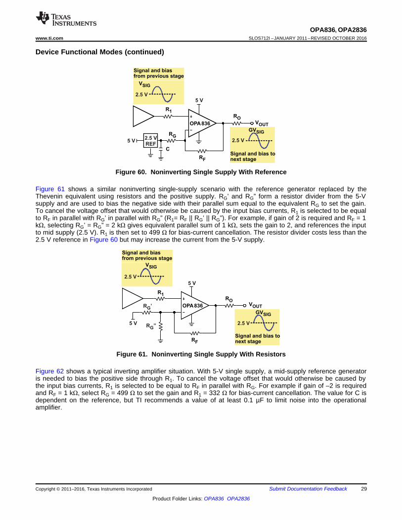
OPA836
Signal and bias tonext stage
Signal and biasfrom previous stage
2.5 V
2.5 V
5 V
R1
R ’G
R ”G
RF
ROVOUT
GVSIG
5 V
VSIG
OPA836
Signal and bias tonext stage
Signal and biasfrom previous stage
C
VSIG
2.5 V
R1
RG
5 V
RF
RO
2.5 V
VOUT
GVSIG
5 V2.5 VREF
29
OPA836, OPA2836www.ti.com SLOS712I –JANUARY 2011–REVISED OCTOBER 2016
Product Folder Links: OPA836 OPA2836
Submit Documentation FeedbackCopyright © 2011–2016, Texas Instruments Incorporated
Device Functional Modes (continued)
Figure 60. Noninverting Single Supply With Reference
Figure 61 shows a similar noninverting single-supply scenario with the reference generator replaced by theThevenin equivalent using resistors and the positive supply. RG’ and RG” form a resistor divider from the 5-Vsupply and are used to bias the negative side with their parallel sum equal to the equivalent RG to set the gain.To cancel the voltage offset that would otherwise be caused by the input bias currents, R1 is selected to be equalto RF in parallel with RG’ in parallel with RG” (R1= RF || RG’ || RG”). For example, if gain of 2 is required and RF = 1kΩ, selecting RG’ = RG” = 2 kΩ gives equivalent parallel sum of 1 kΩ, sets the gain to 2, and references the inputto mid supply (2.5 V). R1 is then set to 499 Ω for bias-current cancellation. The resistor divider costs less than the2.5 V reference in Figure 60 but may increase the current from the 5-V supply.
Figure 61. Noninverting Single Supply With Resistors
Figure 62 shows a typical inverting amplifier situation. With 5-V single supply, a mid-supply reference generatoris needed to bias the positive side through R1. To cancel the voltage offset that would otherwise be caused bythe input bias currents, R1 is selected to be equal to RF in parallel with RG. For example if gain of –2 is requiredand RF = 1 kΩ, select RG = 499 Ω to set the gain and R1 = 332 Ω for bias-current cancellation. The value for C isdependent on the reference, but TI recommends a value of at least 0.1 µF to limit noise into the operationalamplifier.

OPA836
Signal and bias tonext stage
Signal and biasfrom previous stage
C
5 V
2.5 V
R1
R2
5 V
RO
VOUT
RG RF
VSIG
GVSIG
2.5 V
OPA836 VOUT
Signal and bias tonext stage
Signal and biasfrom previous stage
C
R1
RO
RFRG
VSIG
GVSIG
5 V
5 V2.5 VREF
2.5 V
2.5 V
30
OPA836, OPA2836SLOS712I –JANUARY 2011–REVISED OCTOBER 2016 www.ti.com
Product Folder Links: OPA836 OPA2836
Submit Documentation Feedback Copyright © 2011–2016, Texas Instruments Incorporated
Device Functional Modes (continued)
Figure 62. Inverting Single Supply With Reference
Figure 63 shows a similar inverting single-supply scenario with the reference generator replaced by the Theveninequivalent using resistors and the positive supply. R1 and R2 form a resistor divider from the 5-V supply and areused to bias the positive side. To cancel the voltage offset that would otherwise be caused by the input biascurrents, set the parallel sum of R1 and R2 equal to the parallel sum of RF and RG. C must be added to limitcoupling of noise into the positive input. For example if gain of –2 is required and RF = 1 kΩ, select RG = 499 Ωto set the gain. R1 = R2 = 665 Ω for mid-supply voltage bias and for operational amplifier input bias-currentcancellation. A good value for C is 0.1 µF. The resistor divider costs less than the 2.5-V reference in Figure 62but may increase the current from the 5-V supply.
Figure 63. Inverting Single Supply With Resistors

( ) F1 F2IN+ IN REF
G1 G2
2R RV = V V 1 + + V
OUT R R-
æ ö æ ö- ´ç ÷ ç ÷
è ø è ø
- F
G
RG =
R
FSIG REF
G
RV = V + V
OUT R
æ ö-ç ÷è ø
F
G
RG = 1 +
R
æ öç ÷è ø
FSIG REF
G
RV = V 1 + + V
OUT R
31
OPA836, OPA2836www.ti.com SLOS712I –JANUARY 2011–REVISED OCTOBER 2016
Product Folder Links: OPA836 OPA2836
Submit Documentation FeedbackCopyright © 2011–2016, Texas Instruments Incorporated
9 Application and Implementation
NOTEInformation in the following applications sections is not part of the TI componentspecification, and TI does not warrant its accuracy or completeness. TI’s customers areresponsible for determining suitability of components for their purposes. Customers shouldvalidate and test their design implementation to confirm system functionality.
9.1 Application Information
9.1.1 Noninverting AmplifierThe OPA836 and OPA2836 devices can be used as noninverting amplifiers with signal input to the noninvertinginput, VIN+ . A basic block diagram of the circuit is shown in Figure 53.
If VIN = VREF + VSIG, then the output of the amplifier may be calculated according to Equation 1.
(1)
The signal gain of the circuit is set by , and VREF provides a reference around which the input andoutput signals swing. Output signals are in-phase with the input signals.
The OPA836 and OPA2836 devices are designed for the nominal value of RF to be 1 kΩ in gains other than +1.This gives excellent distortion performance, maximum bandwidth, best flatness, and best pulse response. RF = 1kΩ must be used as a default unless other design goals require changing to other values. All test circuits used tocollect data for this data sheet had RF = 1 kΩ for all gains other than +1. Gain of +1 is a special case where RF isshorted and RG is left open.
9.1.2 Inverting AmplifierThe OPA836 and OPA2836 devices can be used as inverting amplifiers with signal input to the inverting input,VIN– , through the gain setting resistor RG. A basic block diagram of the circuit is shown in Figure 54.
If VIN = VREF + VSIG, then the output of the amplifier may be calculated according to Equation 2.
(2)
The signal gain of the circuit is set by , and VREF provides a reference point around which the inputand output signals swing. Output signals are 180° out-of-phase with the input signals. The nominal value of RFmust be 1 kΩ for inverting gains.
9.1.3 Instrumentation AmplifierFigure 64 is an instrumentation amplifier that combines the high input impedance of the differential-to-differentialamplifier circuit and the common-mode rejection of the differential-to-single-ended amplifier circuit. This circuit isoften used in applications where high input impedance is required (such as taps from a differential line) or incases where the signal source has a high output impedance.
If VIN+ = VCM + VSIG+ and VIN– = VCM + VSIG– , then the output of the amplifier may be calculated according toEquation 3.
(3)

VOUT+
RO
+ VOUT-
R
2R2R
½ OPA2836
+
RFRG
VREF
VREF
VIN
R1VSIG
VREF
-G x VSIG
VREF
VREF
G x VSIG
½ OPA2836
RO
F
IN REF IN REFOUT+ OUT-G
RV = G x V + V and V = -G x V + V Where: G = 1 +
R
OPA836
½ OPA2836
VIN-
VIN+
VSIG-
VSIG+
VCM
VCM
RG1
RF1
RF1
RG2
RG2
RF2
RF2
VOUT
G[(V )-(SIG+ V )]SIG-
VREF
VREF
½ OPA2836
æ ö æ öç ÷ ç ÷è ø è ø
F1 F2
G1 G2
2R RG = 1 +
R R
32
OPA836, OPA2836SLOS712I –JANUARY 2011–REVISED OCTOBER 2016 www.ti.com
Product Folder Links: OPA836 OPA2836
Submit Documentation Feedback Copyright © 2011–2016, Texas Instruments Incorporated
Application Information (continued)
The signal gain of the circuit is set by . VCM is rejected, and VREF provides a level shiftaround which the output signal swings. The single-ended output signal is in-phase with the differential inputsignal.
Figure 64. Instrumentation Amplifier
Integrated solutions are available, but the OPA836 device provides a much lower-power, high-frequency solution.For best CMRR performance, resistors must be matched. A good guideline to follow is CMRR ≈ the resistortolerance; so, 0.1% tolerance will provide approximately 60-dB CMRR.
9.1.4 AttenuatorsThe noninverting circuit of Figure 53 has minimum gain of 1. To implement attenuation, a resistor divider can beplaced in series with the positive input, and the amplifier set for gain of 1 by shorting VOUT to VIN– and removingRG. Because the operational amplifier input is high impedance, the resistor divider sets the attenuation.
The inverting circuit of Figure 54 can be used as an attenuator by making RG larger than RF. The attenuation isthe resistor ratio. For example, a 10:1 attenuator can be implemented with RF = 1 kΩ and RG = 10 kΩ.
9.1.5 Single-Ended-to-Differential AmplifierFigure 65 shows an amplifier circuit that is used to convert single-ended signals to differential, and provides gainand level shifting. This circuit can be used for converting signals to differential in applications like line drivers forCat5 cabling or driving differential-input SAR and ΔΣ ADCs.
With VIN = VREF + VSIG , the output of the amplifier may be calculated according to Equation 4.
(4)
The differential-signal gain of the circuit is 2 × G, and VREF provides a reference around which the output signalswings. The differential output signal is in-phase with the single-ended input signal.
Figure 65. Single Ended to Differential Amplifier

OPA836VIN+
VIN-
VCM
VCM
RG
RG
RF
RF
VREF
VSIG-
VSIG+
G[(V )-(SIG+ V )]SIG-
VOUT
VREF
F
G
RG =
R
( )-
æ ö- ´ç ÷
è ø
FOUT IN+ IN REF
G
RV = V V + V
R
VOUT+
49.9 Ω
+ VOUT-
499 Ω
1 kΩ
½ OPA2836
+
VREF
VIN
VSIG
VREF
-VSIG
VREF
VREF
VSIG
½ OPA2836RG RF
49.9 Ω
1 kΩ
33
OPA836, OPA2836www.ti.com SLOS712I –JANUARY 2011–REVISED OCTOBER 2016
Product Folder Links: OPA836 OPA2836
Submit Documentation FeedbackCopyright © 2011–2016, Texas Instruments Incorporated
Application Information (continued)Line termination on the output can be accomplished with resistors RO. The differential impedance seen from theline will be 2 × RO. For example, if 100-Ω Cat5 cable is used with double termination, the amplifier is typically setfor a differential gain of 2 V/V (6 dB) with RF = 0 Ω (short), RG = open, 2R = 1 kΩ, R1 = 0 Ω, R = 499 Ω tobalance the input bias currents, and RO = 49.9 Ω for output line termination. This configuration is shown inFigure 66.
For driving a differential-input ADC the situation is similar, but the output resistors, RO are selected with acapacitor across the ADC input for optimum filtering and settling-time performance.
Figure 66. Cat5 Line Driver With Gain = 2 V/V (6 dB)
9.1.6 Differential-to-Signal-Ended AmplifierFigure 67 shows a differential amplifier that is used to convert differential signals to single-ended and providesgain (or attenuation) and level shifting. This circuit can be used in applications like a line receiver for converting adifferential signal from a Cat5 cable to a single-ended signal.
If VIN+ = VCM + VSIG+ and VIN– = VCM + VSIG– , then the output of the amplifier may be calculated according toEquation 5.
(5)
The signal gain of the circuit is , VCM is rejected, and VREF provides a level shift around which theoutput signal swings. The single ended output signal is in-phase with the differential input signal.
Figure 67. Differential to Single-Ended Amplifier
Line termination can be accomplished by adding a shunt resistor across the VIN+ and VIN- inputs. Thedifferential impedance is the shunt resistance in parallel with the input impedance of the amplifier circuit, which isusually much higher. For low gain and low line impedance, the resistor value to add is approximately theimpedance of the line. For example if 100-Ω Cat5 cable is used with a gain of 1 amplifier and RF = RG = 1 kΩ,adding a 100-Ω shunt across the input will give a differential impedance of 98 Ω, which is adequate for mostapplications.
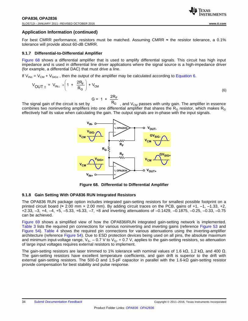
½ OPA2836
½ OPA2836
GVSIG-
VIN-
VSIG-
VSIG+
VCM
VCM
RG
RF
RF
VIN+
VOUT-
VOUT+
VCM
VCM
GVSIG+
F
G
2RG = 1 +
R
±
æ ö´ç ÷±
è ø
FIN CM
G
2RV = V 1 + + V
OUT R
34
OPA836, OPA2836SLOS712I –JANUARY 2011–REVISED OCTOBER 2016 www.ti.com
Product Folder Links: OPA836 OPA2836
Submit Documentation Feedback Copyright © 2011–2016, Texas Instruments Incorporated
Application Information (continued)For best CMRR performance, resistors must be matched. Assuming CMRR ≈ the resistor tolerance, a 0.1%tolerance will provide about 60-dB CMRR.
9.1.7 Differential-to-Differential AmplifierFigure 68 shows a differential amplifier that is used to amplify differential signals. This circuit has high inputimpedance and is used in differential line driver applications where the signal source is a high-impedance driver(for example, a differential DAC) that must drive a line.
If VIN± = VCM + VSIG± , then the output of the amplifier may be calculated according to Equation 6.
(6)
The signal gain of the circuit is set by , and VCM passes with unity gain. The amplifier in essencecombines two noninverting amplifiers into one differential amplifier that shares the RG resistor, which makes RGeffectively half its value when calculating the gain. The output signals are in-phase with the input signals.
Figure 68. Differential to Differential Amplifier
9.1.8 Gain Setting With OPA836 RUN Integrated ResistorsThe OPA836 RUN package option includes integrated gain-setting resistors for smallest possible footprint on aprinted circuit board (≈ 2.00 mm × 2.00 mm). By adding circuit traces on the PCB, gains of +1, –1, –1.33, +2,+2.33, –3, +4, –4, +5, –5.33, +6.33, –7, +8 and inverting attenuations of –0.1429, –0.1875, –0.25, –0.33, –0.75can be achieved.
Figure 69 shows a simplified view of how the OPA836IRUN integrated gain-setting network is implemented.Table 3 lists the required pin connections for various noninverting and inverting gains (reference Figure 53 andFigure 54). Table 4 shows the required pin connections for various attenuations using the inverting-amplifierarchitecture (reference Figure 54). Due to ESD protection devices being used on all pins, the absolute maximumand minimum input-voltage range, VS– – 0.7 V to VS+ + 0.7 V, applies to the gain-setting resistors, so attenuationof large input voltages requires external resistors to implement.
The gain-setting resistors are laser trimmed to 1% tolerance with nominal values of 1.6 kΩ, 1.2 kΩ, and 400 Ω.The gain-setting resistors have excellent temperature coefficients, and gain drift is superior to the drift withexternal gain-setting resistors. The 500-Ω and 1.5-pF capacitor in parallel with the 1.6-kΩ gain-setting resistorprovide compensation for best stability and pulse response.

RF
OPA836
Signal and biasfrom previous stage
Signal and bias tonext stage
5 V
R1
RG
0 V
VSIG
ROVOUT
GVSIG
0 V
FB1 FB2 FB3 FB4
9 8 67
1.6 k 1.2 k 400
500 1.5 pF
35
OPA836, OPA2836www.ti.com SLOS712I –JANUARY 2011–REVISED OCTOBER 2016
Product Folder Links: OPA836 OPA2836
Submit Documentation FeedbackCopyright © 2011–2016, Texas Instruments Incorporated
Application Information (continued)
Figure 69. OPA836IRUN Gain-Setting Network
Table 3. Gain SettingsNONINVERTING GAIN
(Figure 53)INVERTING GAIN
(Figure 54) SHORT PINS SHORT PINS SHORT PINS SHORT PINS
1 V/V (0 dB) — 1 to 9 —2 V/V (6.02 dB) –1 V/V (0 dB) 1 to 9 2 to 8 6 to GND —
2.33 V/V (7.36 dB) –1.33 V/V (2.5 dB) 1 to 9 2 to 8 7 to GND —4 V/V (12.04 dB) –3 V/V (9.54 dB) 1 to 8 2 to 7 6 to GND —5 V/V (13.98 dB) –4 V/V (12.04 dB) 1 to 9 2 to 7 or 8 7 to 8 6 to GND
6.33 V/V (16.03 dB) –5.33 V/V (14.54 dB) 1 to 9 2 to 6 or 8 6 to 8 7 to GND8 V/V (18.06 dB) –7 V/V (16.90 dB) 1 to 9 2 to 7 6 to GND —
Table 4. Attenuator SettingsINVERTING GAIN
(Figure 54) SHORT PINS SHORT PINS SHORT PINS SHORT PINS
–0.75 V/V (–2.5 dB) 1 to 7 2 to 8 9 to GND —–0.333 V/V (–9.54 dB) 1 to 6 2 to 7 8 to GND —–0.25 V/V (–12.04 dB) 1 to 6 2 to 7 or 8 7 to 8 9 to GND
–0.1875 V/V (–14.54 dB) 1 to 7 2 to 6 or 8 6 to 8 9 to GND–0.1429 V/V (–16.90 dB) 1 to 6 2 to 7 9 to GND —
9.1.9 Pulse Application With Single-SupplyFor pulsed applications, where the signal is at ground and pulses to a positive or negative voltage, the circuitbias-voltage considerations differ from those in an application with a signal that swings symmetrical about areference point. Figure 70 shows a circuit where the signal is at ground (0 V) and pulses to a positive value.
Figure 70. Noninverting Single Supply With Pulse

2.7V
ADS 8326
+In
-In
100
2.2 nF
1k
1k
VIN
OPA836
VS-
1k
2k
2 k
2.5 V5 VVS+
VDD REF
2.7 V
0 V
VSIG
1.35 V
VSIG
OPA836
Signal and biasfrom previous stage Signal and bias to
next stage
5 V
R1
RG
RF
GVSIG
0 V
0 V
VSIG
VOUT
RO
36
OPA836, OPA2836SLOS712I –JANUARY 2011–REVISED OCTOBER 2016 www.ti.com
Product Folder Links: OPA836 OPA2836
Submit Documentation Feedback Copyright © 2011–2016, Texas Instruments Incorporated
If the input signal pulses negative from ground, an inverting amplifier is more appropriate as shown in Figure 71.A key consideration in noninverting and inverting cases is that the input and output voltages are kept within thelimits of the amplifier. Because the VICR of the OPA836 device includes the negative supply rail, the OPA836operational amplifier is well-suited to this application.
Figure 71. Inverting Single Supply With Pulse
9.1.10 ADC Driver PerformanceThe OPA836 device provides excellent performance when driving high-performance delta-sigma (ΔΣ) andsuccessive-approximation-register (SAR) ADCs in low-power audio and industrial applications.
To show achievable performance, the OPA836 device is tested as the drive amplifier for the ADS8326. TheADS8326 is a 16-bit, micro power, SAR ADC with pseudodifferential inputs and sample rates up to 250 kSPS.The device offers excellent noise and distortion performance in a small 8-pin SOIC or VSSOP (MSOP) package.Low power and small size make the ADS8326 and OPA836 devices an ideal solution for portable and battery-operated systems, remote data-acquisition modules, simultaneous multichannel systems, and isolated dataacquisition.
With the circuit shown in Figure 72 to test the performance, Figure 73 shows the FFT plot with a 10-kHz inputsignal . The tabulated AC analysis is in Table 5.
Figure 72. OPA836 and ADS8326 Test Circuit
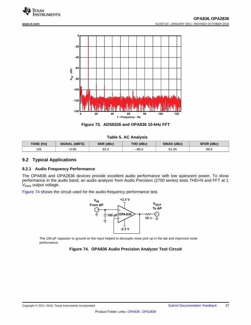
OPA83610 W
100 pF
V
From APIN
+2.5 V
-2.5 V
V
To APOUT
-140
-120
-100
-80
-60
-40
-20
0
0 20 40 60 80 100 120f - Frequency - Hz
A-
dB
cIN
37
OPA836, OPA2836www.ti.com SLOS712I –JANUARY 2011–REVISED OCTOBER 2016
Product Folder Links: OPA836 OPA2836
Submit Documentation FeedbackCopyright © 2011–2016, Texas Instruments Incorporated
Figure 73. ADS8326 and OPA836 10-kHz FFT
Table 5. AC AnalysisTONE (Hz) SIGNAL (dBFS) SNR (dBc) THD (dBc) SINAD (dBc) SFDR (dBc)
10k –0.85 83.3 –86.6 81.65 88.9
9.2 Typical Applications
9.2.1 Audio Frequency PerformanceThe OPA836 and OPA2836 devices provide excellent audio performance with low quiescent power. To showperformance in the audio band, an audio analyzer from Audio Precision (2700 series) tests THD+N and FFT at 1VRMS output voltage.
Figure 74 shows the circuit used for the audio-frequency performance test.
The 100-pF capacitor to ground on the input helped to decouple noise pick up in the lab and improved noiseperformance.
Figure 74. OPA836 Audio Precision Analyzer Test Circuit

38
OPA836, OPA2836SLOS712I –JANUARY 2011–REVISED OCTOBER 2016 www.ti.com
Product Folder Links: OPA836 OPA2836
Submit Documentation Feedback Copyright © 2011–2016, Texas Instruments Incorporated
Typical Applications (continued)9.2.1.1 Design RequirementsDesign a low distortion, single-ended input to single-ended output audio amplifier using the OPA836 device. The2700-series audio analyzer from Audio Precision is used as the signal source and also as the measurementsystem.
Table 6. Design Requirements
CONFIGURATION INPUTEXCITATION
PERFORMANCETARGET RLoad
OPA836 Unity Gain Config. 1 KHz Tone Frequency >110 dBc SFDR 300 Ω and100 kΩ
9.2.1.2 Detailed Design ProcedureThe OPA836 device is tested in this application in a unity-gain buffer configuration. A buffer configuration isselected for maximum loop gain of the amplifier circuit. At higher closed-loop gains, the loop gain of the circuitreduces, which increases the harmonic distortion. The relationship between distortion and closed-loop gain at afixed input frequency is shown in Figure 36 in Typical Performance Graphs: VS = 5 V. The test was performedunder using resistive loads of 300 Ω and 100 KΩ. Figure 34 shows the distortion performance of the amplifierversus the resistive load. Output loading, output swing, and closed-loop gain play a key role in determining thedistortion performance of the amplifier.
NOTEThe 100-pF capacitor to ground on the input helped to decouple noise pickup in the laband improved noise performance.
The Audio Precision was configured as a single-ended output in this application circuit. In applications where adifferential output is available, the OPA836 device can be configured as a differential-to-single-ended amplifier asshown in Figure 67. Power-supply bypassing is critical to reject noise from the power supplies. A 2.2-μF supplydecoupling capacitor must be placed within 2 inches of the device and can be shared with other operationalamplifiers on the same board. A 0.1-μF supply decoupling capacitor must be placed as close to the supply pinsas possible, preferably within 0.1 inch. For a split supply, a capacitor is required for both supplies. A 0.1-µFcapacitor placed directly between the supplies is also beneficial for improving system noise performance. If theoutput load is heavy, such as 16 Ω to 32 Ω, performance of the amplifier could begin to degrade. To drive suchheavy loads, both channels of the OPA2836 device can be paralleled with their outputs isolated with 1-Ωresistors to reduce the loading effects.

-140
-130
-120
-110
-100
-90
-80
-70
-60
-50
-40
-30
-20
-10
0
FF
T -
dB
V
0 2k 4k 6k 8k 10k 12k 14 16k 18k 20k
f - Frequency - Hz
V = 5 V,
V = 1 V ,
G = 1,
R = 0
S
OUT RMS
F W
R = 300L
Gen Mon - 300
10 100 1k 10k 100kf - Frequency - Hz
No weighting
R = 300 ,L W
R = 100 kL W
-120
-115
-110
-105
-100
-95
-90
TH
D+
N -
To
tal
Ha
rmo
nic
Dis
tort
ion
+ N
ois
e -
dB
v V = 5 V,
V = 1 V ,
G = 1,
R = 0 ,
BW = 80 kHz
S
OUT RMS
F W
A-weighting
R = 300 ,L W
R = 100 kL W
0 2k 4k 6k 8k 10k 12k 14 16k 18k 20k
f - Frequency - Hz
-140
-130
-120
-110
-100
-90
-80
-70
-60
-50
-40
-30
-20
-10
0
FF
T -
dB
V
R = 100kL
Gen Mon - 100k
V = 5 V,
V = 1 V ,
G = 1,
R = 0
S
OUT RMS
F W
39
OPA836, OPA2836www.ti.com SLOS712I –JANUARY 2011–REVISED OCTOBER 2016
Product Folder Links: OPA836 OPA2836
Submit Documentation FeedbackCopyright © 2011–2016, Texas Instruments Incorporated
9.2.1.3 Application Curves
Figure 75 shows the THD+N performance with 100-kΩ and 300-Ω loads, and with A-weighting and with noweighting. Both loads show similar performance. With no weighting, the THD+N performance is dominated by thenoise for both loads. A-weighting provides filtering that improves the noise, revealing the increased distortion withRL = 300 Ω.
Figure 76 and Figure 77 show the FFT output with a 1-kHz tone and 100-kΩ and 300-Ω loads. To show relativeperformance of the device versus the test set, one channel has the OPA836 device in-line between the generatoroutput and the analyzer. The other channel is in “Gen Mon” loopback mode, which internally connects the signalgenerator to the analyzer input. With 100-kΩ load, Figure 76, the curves are indistinguishable from each otherexcept for noise, which means the OPA836 device cannot be directly measured. With 300-Ω load, as shown inFigure 77, the main difference between the curves is that the OPA836 device shows slightly higher even-orderharmonics, but the performance of the test set masks the odd-order harmonics.
Figure 75. OPA836 1 VRMS 20-Hz to 80-kHz THD+N Figure 76. OPA836 and AP Gen Mon 10-kHz FFT Plot; VOUT= 1 VRMS, RL = 100 kΩ
Figure 77. OPA836 and AP Gen Mon 10-kHz FFT Plot;VOUT = 1 VRMS, RL = 300 Ω
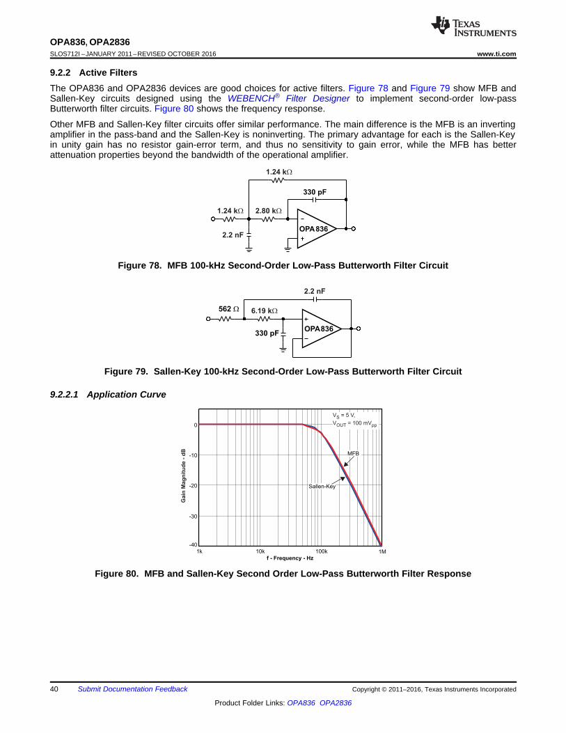
-40
-30
-20
-10
0
1k 10k 100k 1Mf - Frequency - Hz
Sallen-Key
MFB
Gain
Mag
nit
ud
e -
dB
V = 5 V,
V = 100 mVS
OUT pp
OPA836330 pF
562 W 6.19 kW
2.2 nF
OPA836
330 pF
1.24 kW
1.24 kW 2.80 kW
2.2 nF
40
OPA836, OPA2836SLOS712I –JANUARY 2011–REVISED OCTOBER 2016 www.ti.com
Product Folder Links: OPA836 OPA2836
Submit Documentation Feedback Copyright © 2011–2016, Texas Instruments Incorporated
9.2.2 Active FiltersThe OPA836 and OPA2836 devices are good choices for active filters. Figure 78 and Figure 79 show MFB andSallen-Key circuits designed using the WEBENCH® Filter Designer to implement second-order low-passButterworth filter circuits. Figure 80 shows the frequency response.
Other MFB and Sallen-Key filter circuits offer similar performance. The main difference is the MFB is an invertingamplifier in the pass-band and the Sallen-Key is noninverting. The primary advantage for each is the Sallen-Keyin unity gain has no resistor gain-error term, and thus no sensitivity to gain error, while the MFB has betterattenuation properties beyond the bandwidth of the operational amplifier.
Figure 78. MFB 100-kHz Second-Order Low-Pass Butterworth Filter Circuit
Figure 79. Sallen-Key 100-kHz Second-Order Low-Pass Butterworth Filter Circuit
9.2.2.1 Application Curve
Figure 80. MFB and Sallen-Key Second Order Low-Pass Butterworth Filter Response
41
OPA836, OPA2836www.ti.com SLOS712I –JANUARY 2011–REVISED OCTOBER 2016
Product Folder Links: OPA836 OPA2836
Submit Documentation FeedbackCopyright © 2011–2016, Texas Instruments Incorporated
10 Power Supply RecommendationsThe OPAx836 devices are intended to work in a supply range of 2.7 V to 5 V. Supply-voltage tolerances aresupported with the specified operating range of 2.5 V (7% on a 2.7-V supply) and 5.5 V (10% on a 5-V supply).Good power-supply bypassing is required. Minimize the distance (< 0.1 inch) from the power-supply pins to highfrequency, 0.1-μF decoupling capacitors. A larger capacitor (2.2 µF is typical) is used along with a highfrequency, 0.1-µF supply decoupling capacitor at the device supply pins. For single-supply operation, only thepositive supply has these capacitors. When a split supply is used, use these capacitors for each supply toground. If necessary, place the larger capacitors farther from the device and share these capacitors amongseveral devices in the same area of the PCB. Avoid narrow power and ground traces to minimize inductancebetween the pins and the decoupling capacitors. An optional supply decoupling capacitor across the two powersupplies (for bipolar operation) reduces second harmonic distortion.
11 Layout
11.1 Layout GuidelinesThe OPA835DBV, OPA836DBV EVM (SLOU314) can be used as a reference when designing the circuit board.TI recommends following the EVM layout of the external components near the amplifier, ground-planeconstruction, and power routing. General guidelines are listed as follows:1. Signal routing must be direct and as short as possible into and out of the operational amplifier.2. The feedback path must be short and direct avoiding vias if possible especially with G = +1.3. Ground or power planes must be removed from directly under the negative input and output pins of the
amplifier.4. TI recommends placing a series output resistor as close to the output pin as possible. See Series Output
Resistor vs Capacitive Load (Figure 17) for recommended values for the expected capacitive load.5. A 2.2-µF power-supply decoupling capacitor must be placed within two inches of the device and can be
shared with other operational amplifiers. For spit supply, a capacitor is required for both supplies.6. A 0.1-µF power-supply decoupling capacitor must be placed as close to the power supply pins as possible,
preferably within 0.1 inch. For split supply, a capacitor is required for both supplies.7. The PD pin uses TTL logic levels. If the pin is not used, it must be tied to the positive supply to enable the
amplifier. If the pin is used, it must be actively driven. A bypass capacitor is not necessary, but is used forrobustness in noisy environments.
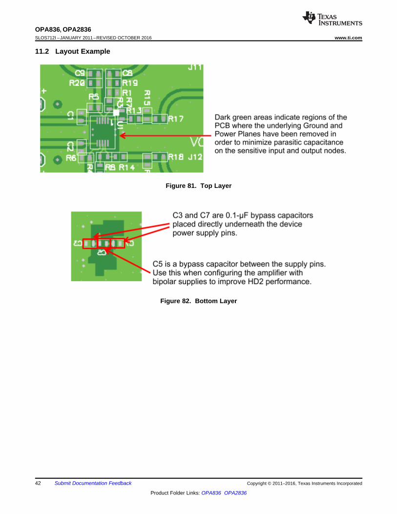
42
OPA836, OPA2836SLOS712I –JANUARY 2011–REVISED OCTOBER 2016 www.ti.com
Product Folder Links: OPA836 OPA2836
Submit Documentation Feedback Copyright © 2011–2016, Texas Instruments Incorporated
11.2 Layout Example
Figure 81. Top Layer
Figure 82. Bottom Layer

43
OPA836, OPA2836www.ti.com SLOS712I –JANUARY 2011–REVISED OCTOBER 2016
Product Folder Links: OPA836 OPA2836
Submit Documentation FeedbackCopyright © 2011–2016, Texas Instruments Incorporated
12 Device and Documentation Support
12.1 Device Support
12.1.1 Development SupportWEBENCH® Filter Designer
12.1.2 Related DocumentationFor related documentation see the following:
OPA835DBV, OPA836DBV EVM (SLOU314).
12.2 Related LinksTable 7 lists quick access links. Categories include technical documents, support and community resources,tools and software, and quick access to sample or buy.
Table 7. Related Links
PARTS PRODUCT FOLDER SAMPLE & BUY TECHNICALDOCUMENTS
TOOLS &SOFTWARE
SUPPORT &COMMUNITY
OPA836 Click here Click here Click here Click here Click hereOPA2836 Click here Click here Click here Click here Click here
12.3 Receiving Notification of Documentation UpdatesTo receive notification of documentation updates, navigate to the device product folder on ti.com. In the upperright corner, click on Alert me to register and receive a weekly digest of any product information that haschanged. For change details, review the revision history included in any revised document.
12.4 Community ResourcesThe following links connect to TI community resources. Linked contents are provided "AS IS" by the respectivecontributors. They do not constitute TI specifications and do not necessarily reflect TI's views; see TI's Terms ofUse.
TI E2E™ Online Community TI's Engineer-to-Engineer (E2E) Community. Created to foster collaborationamong engineers. At e2e.ti.com, you can ask questions, share knowledge, explore ideas and helpsolve problems with fellow engineers.
Design Support TI's Design Support Quickly find helpful E2E forums along with design support tools andcontact information for technical support.
12.5 TrademarksE2E is a trademark of Texas Instruments.WEBENCH is a registered trademark of Texas Instruments.All other trademarks are the property of their respective owners.
12.6 Electrostatic Discharge CautionThis integrated circuit can be damaged by ESD. Texas Instruments recommends that all integrated circuits be handled withappropriate precautions. Failure to observe proper handling and installation procedures can cause damage.
ESD damage can range from subtle performance degradation to complete device failure. Precision integrated circuits may be moresusceptible to damage because very small parametric changes could cause the device not to meet its published specifications.
12.7 GlossarySLYZ022 — TI Glossary.
This glossary lists and explains terms, acronyms, and definitions.
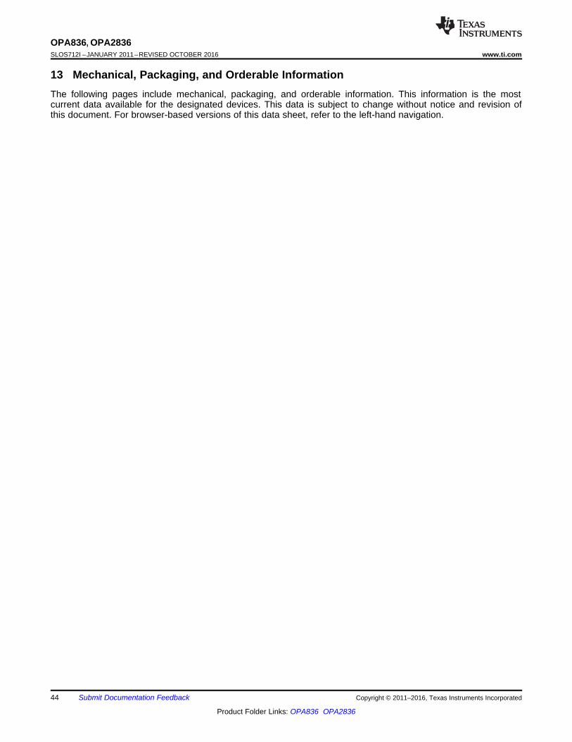
44
OPA836, OPA2836SLOS712I –JANUARY 2011–REVISED OCTOBER 2016 www.ti.com
Product Folder Links: OPA836 OPA2836
Submit Documentation Feedback Copyright © 2011–2016, Texas Instruments Incorporated
13 Mechanical, Packaging, and Orderable InformationThe following pages include mechanical, packaging, and orderable information. This information is the mostcurrent data available for the designated devices. This data is subject to change without notice and revision ofthis document. For browser-based versions of this data sheet, refer to the left-hand navigation.

PACKAGE OPTION ADDENDUM
www.ti.com 4-Dec-2017
Addendum-Page 1
PACKAGING INFORMATION
Orderable Device Status(1)
Package Type PackageDrawing
Pins PackageQty
Eco Plan(2)
Lead/Ball Finish(6)
MSL Peak Temp(3)
Op Temp (°C) Device Marking(4/5)
Samples
OPA2836ID ACTIVE SOIC D 8 75 Green (RoHS& no Sb/Br)
CU NIPDAU Level-2-260C-1 YEAR -40 to 125 2836
OPA2836IDGS ACTIVE VSSOP DGS 10 80 Green (RoHS& no Sb/Br)
CU NIPDAUAG Level-2-260C-1 YEAR -40 to 125 2836
OPA2836IDGSR ACTIVE VSSOP DGS 10 2500 Green (RoHS& no Sb/Br)
CU NIPDAUAG Level-2-260C-1 YEAR -40 to 125 2836
OPA2836IDR ACTIVE SOIC D 8 2500 Green (RoHS& no Sb/Br)
CU NIPDAU Level-2-260C-1 YEAR -40 to 125 2836
OPA2836IRMCR ACTIVE UQFN RMC 10 3000 Green (RoHS& no Sb/Br)
CU NIPDAU Level-2-260C-1 YEAR -40 to 125 2836
OPA2836IRMCT ACTIVE UQFN RMC 10 250 Green (RoHS& no Sb/Br)
CU NIPDAU Level-2-260C-1 YEAR -40 to 125 2836
OPA2836IRUNR ACTIVE QFN RUN 10 3000 Green (RoHS& no Sb/Br)
CU NIPDAU Level-2-260C-1 YEAR -40 to 125 2836
OPA2836IRUNT ACTIVE QFN RUN 10 250 Green (RoHS& no Sb/Br)
CU NIPDAU Level-2-260C-1 YEAR -40 to 125 2836
OPA836IDBVR ACTIVE SOT-23 DBV 6 3000 Green (RoHS& no Sb/Br)
CU SN Level-1-260C-UNLIM -40 to 125 QTL
OPA836IDBVT ACTIVE SOT-23 DBV 6 250 Green (RoHS& no Sb/Br)
CU SN Level-1-260C-UNLIM -40 to 125 QTL
OPA836IRUNR ACTIVE QFN RUN 10 3000 Green (RoHS& no Sb/Br)
CU NIPDAU Level-2-260C-1 YEAR -40 to 125 836
OPA836IRUNT ACTIVE QFN RUN 10 250 Green (RoHS& no Sb/Br)
CU NIPDAU Level-2-260C-1 YEAR -40 to 125 836
(1) The marketing status values are defined as follows:ACTIVE: Product device recommended for new designs.LIFEBUY: TI has announced that the device will be discontinued, and a lifetime-buy period is in effect.NRND: Not recommended for new designs. Device is in production to support existing customers, but TI does not recommend using this part in a new design.PREVIEW: Device has been announced but is not in production. Samples may or may not be available.OBSOLETE: TI has discontinued the production of the device.
(2) RoHS: TI defines "RoHS" to mean semiconductor products that are compliant with the current EU RoHS requirements for all 10 RoHS substances, including the requirement that RoHS substancedo not exceed 0.1% by weight in homogeneous materials. Where designed to be soldered at high temperatures, "RoHS" products are suitable for use in specified lead-free processes. TI mayreference these types of products as "Pb-Free".RoHS Exempt: TI defines "RoHS Exempt" to mean products that contain lead but are compliant with EU RoHS pursuant to a specific EU RoHS exemption.
PACKAGE OPTION ADDENDUM
www.ti.com 4-Dec-2017
Addendum-Page 2
Green: TI defines "Green" to mean the content of Chlorine (Cl) and Bromine (Br) based flame retardants meet JS709B low halogen requirements of <=1000ppm threshold. Antimony trioxide basedflame retardants must also meet the <=1000ppm threshold requirement.
(3) MSL, Peak Temp. - The Moisture Sensitivity Level rating according to the JEDEC industry standard classifications, and peak solder temperature.
(4) There may be additional marking, which relates to the logo, the lot trace code information, or the environmental category on the device.
(5) Multiple Device Markings will be inside parentheses. Only one Device Marking contained in parentheses and separated by a "~" will appear on a device. If a line is indented then it is a continuationof the previous line and the two combined represent the entire Device Marking for that device.
(6) Lead/Ball Finish - Orderable Devices may have multiple material finish options. Finish options are separated by a vertical ruled line. Lead/Ball Finish values may wrap to two lines if the finishvalue exceeds the maximum column width.
Important Information and Disclaimer:The information provided on this page represents TI's knowledge and belief as of the date that it is provided. TI bases its knowledge and belief on informationprovided by third parties, and makes no representation or warranty as to the accuracy of such information. Efforts are underway to better integrate information from third parties. TI has taken andcontinues to take reasonable steps to provide representative and accurate information but may not have conducted destructive testing or chemical analysis on incoming materials and chemicals.TI and TI suppliers consider certain information to be proprietary, and thus CAS numbers and other limited information may not be available for release.
In no event shall TI's liability arising out of such information exceed the total purchase price of the TI part(s) at issue in this document sold by TI to Customer on an annual basis.
OTHER QUALIFIED VERSIONS OF OPA2836 :
• Automotive: OPA2836-Q1
NOTE: Qualified Version Definitions:
• Automotive - Q100 devices qualified for high-reliability automotive applications targeting zero defects

TAPE AND REEL INFORMATION
*All dimensions are nominal
Device PackageType
PackageDrawing
Pins SPQ ReelDiameter
(mm)
ReelWidth
W1 (mm)
A0(mm)
B0(mm)
K0(mm)
P1(mm)
W(mm)
Pin1Quadrant
OPA2836IDGSR VSSOP DGS 10 2500 330.0 12.4 5.3 3.4 1.4 8.0 12.0 Q1
OPA2836IDR SOIC D 8 2500 330.0 12.4 6.4 5.2 2.1 8.0 12.0 Q1
OPA2836IRMCR UQFN RMC 10 3000 180.0 9.5 2.3 2.3 1.1 2.0 8.0 Q2
OPA2836IRMCT UQFN RMC 10 250 180.0 9.5 2.3 2.3 1.1 2.0 8.0 Q2
OPA2836IRUNR QFN RUN 10 3000 180.0 8.4 2.3 2.3 1.15 4.0 8.0 Q2
OPA2836IRUNT QFN RUN 10 250 180.0 8.4 2.3 2.3 1.15 4.0 8.0 Q2
OPA836IDBVR SOT-23 DBV 6 3000 178.0 9.0 3.23 3.17 1.37 4.0 8.0 Q3
OPA836IDBVT SOT-23 DBV 6 250 178.0 9.0 3.23 3.17 1.37 4.0 8.0 Q3
OPA836IRUNR QFN RUN 10 3000 180.0 8.4 2.3 2.3 1.15 4.0 8.0 Q2
OPA836IRUNT QFN RUN 10 250 180.0 8.4 2.3 2.3 1.15 4.0 8.0 Q2
PACKAGE MATERIALS INFORMATION
www.ti.com 30-Mar-2017
Pack Materials-Page 1

*All dimensions are nominal
Device Package Type Package Drawing Pins SPQ Length (mm) Width (mm) Height (mm)
OPA2836IDGSR VSSOP DGS 10 2500 366.0 364.0 50.0
OPA2836IDR SOIC D 8 2500 340.5 338.1 20.6
OPA2836IRMCR UQFN RMC 10 3000 205.0 200.0 30.0
OPA2836IRMCT UQFN RMC 10 250 205.0 200.0 30.0
OPA2836IRUNR QFN RUN 10 3000 210.0 185.0 35.0
OPA2836IRUNT QFN RUN 10 250 210.0 185.0 35.0
OPA836IDBVR SOT-23 DBV 6 3000 180.0 180.0 18.0
OPA836IDBVT SOT-23 DBV 6 250 180.0 180.0 18.0
OPA836IRUNR QFN RUN 10 3000 210.0 185.0 35.0
OPA836IRUNT QFN RUN 10 250 210.0 185.0 35.0
PACKAGE MATERIALS INFORMATION
www.ti.com 30-Mar-2017
Pack Materials-Page 2


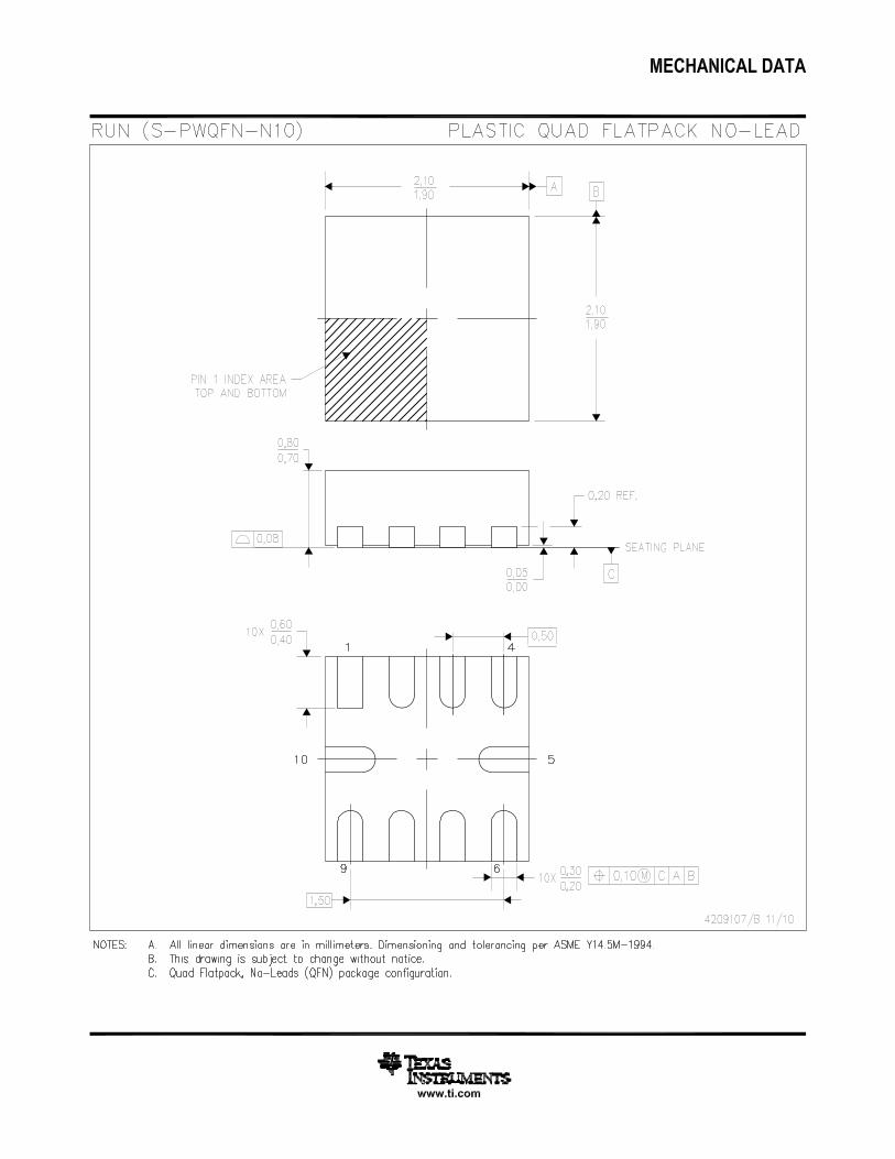


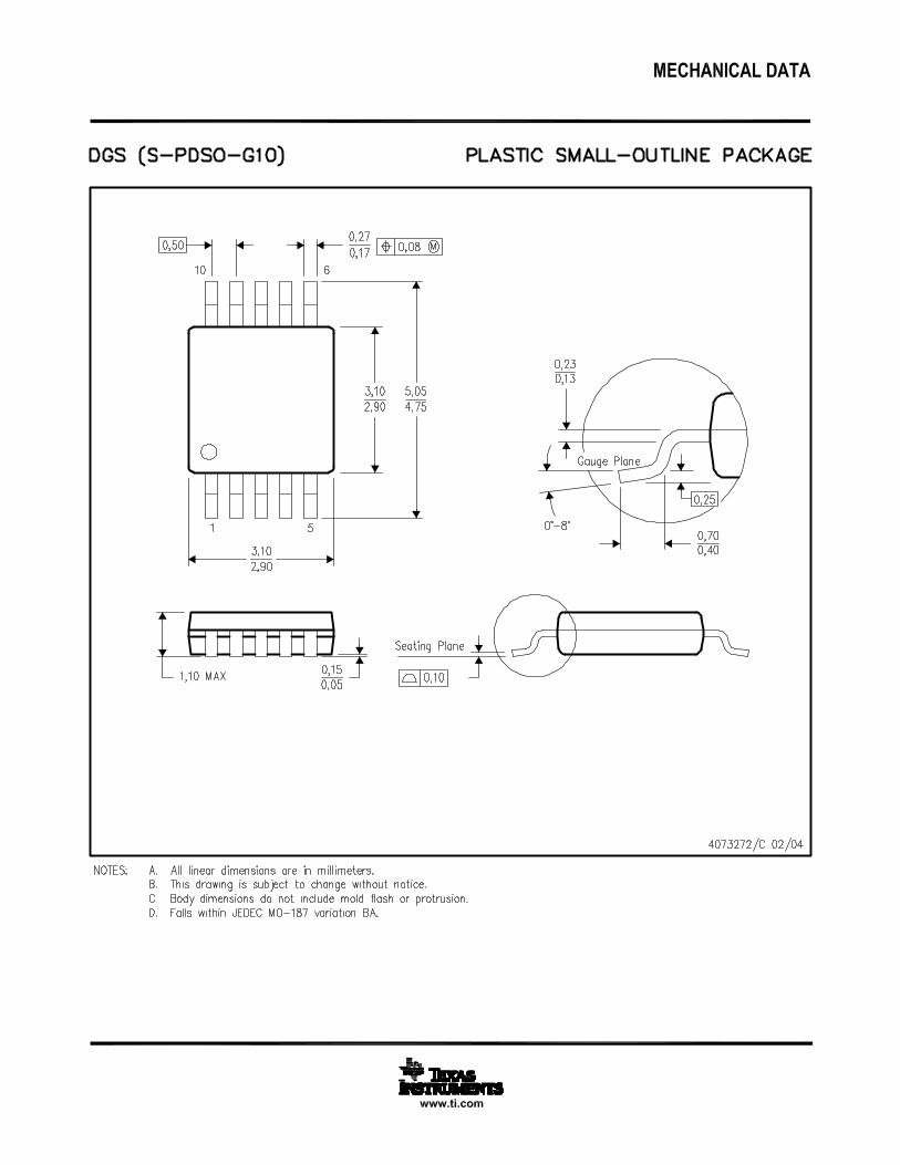

IMPORTANT NOTICE
Texas Instruments Incorporated (TI) reserves the right to make corrections, enhancements, improvements and other changes to itssemiconductor products and services per JESD46, latest issue, and to discontinue any product or service per JESD48, latest issue. Buyersshould obtain the latest relevant information before placing orders and should verify that such information is current and complete.TI’s published terms of sale for semiconductor products (http://www.ti.com/sc/docs/stdterms.htm) apply to the sale of packaged integratedcircuit products that TI has qualified and released to market. Additional terms may apply to the use or sale of other types of TI products andservices.Reproduction of significant portions of TI information in TI data sheets is permissible only if reproduction is without alteration and isaccompanied by all associated warranties, conditions, limitations, and notices. TI is not responsible or liable for such reproduceddocumentation. Information of third parties may be subject to additional restrictions. Resale of TI products or services with statementsdifferent from or beyond the parameters stated by TI for that product or service voids all express and any implied warranties for theassociated TI product or service and is an unfair and deceptive business practice. TI is not responsible or liable for any such statements.Buyers and others who are developing systems that incorporate TI products (collectively, “Designers”) understand and agree that Designersremain responsible for using their independent analysis, evaluation and judgment in designing their applications and that Designers havefull and exclusive responsibility to assure the safety of Designers' applications and compliance of their applications (and of all TI productsused in or for Designers’ applications) with all applicable regulations, laws and other applicable requirements. Designer represents that, withrespect to their applications, Designer has all the necessary expertise to create and implement safeguards that (1) anticipate dangerousconsequences of failures, (2) monitor failures and their consequences, and (3) lessen the likelihood of failures that might cause harm andtake appropriate actions. Designer agrees that prior to using or distributing any applications that include TI products, Designer willthoroughly test such applications and the functionality of such TI products as used in such applications.TI’s provision of technical, application or other design advice, quality characterization, reliability data or other services or information,including, but not limited to, reference designs and materials relating to evaluation modules, (collectively, “TI Resources”) are intended toassist designers who are developing applications that incorporate TI products; by downloading, accessing or using TI Resources in anyway, Designer (individually or, if Designer is acting on behalf of a company, Designer’s company) agrees to use any particular TI Resourcesolely for this purpose and subject to the terms of this Notice.TI’s provision of TI Resources does not expand or otherwise alter TI’s applicable published warranties or warranty disclaimers for TIproducts, and no additional obligations or liabilities arise from TI providing such TI Resources. TI reserves the right to make corrections,enhancements, improvements and other changes to its TI Resources. TI has not conducted any testing other than that specificallydescribed in the published documentation for a particular TI Resource.Designer is authorized to use, copy and modify any individual TI Resource only in connection with the development of applications thatinclude the TI product(s) identified in such TI Resource. NO OTHER LICENSE, EXPRESS OR IMPLIED, BY ESTOPPEL OR OTHERWISETO ANY OTHER TI INTELLECTUAL PROPERTY RIGHT, AND NO LICENSE TO ANY TECHNOLOGY OR INTELLECTUAL PROPERTYRIGHT OF TI OR ANY THIRD PARTY IS GRANTED HEREIN, including but not limited to any patent right, copyright, mask work right, orother intellectual property right relating to any combination, machine, or process in which TI products or services are used. Informationregarding or referencing third-party products or services does not constitute a license to use such products or services, or a warranty orendorsement thereof. Use of TI Resources may require a license from a third party under the patents or other intellectual property of thethird party, or a license from TI under the patents or other intellectual property of TI.TI RESOURCES ARE PROVIDED “AS IS” AND WITH ALL FAULTS. TI DISCLAIMS ALL OTHER WARRANTIES ORREPRESENTATIONS, EXPRESS OR IMPLIED, REGARDING RESOURCES OR USE THEREOF, INCLUDING BUT NOT LIMITED TOACCURACY OR COMPLETENESS, TITLE, ANY EPIDEMIC FAILURE WARRANTY AND ANY IMPLIED WARRANTIES OFMERCHANTABILITY, FITNESS FOR A PARTICULAR PURPOSE, AND NON-INFRINGEMENT OF ANY THIRD PARTY INTELLECTUALPROPERTY RIGHTS. TI SHALL NOT BE LIABLE FOR AND SHALL NOT DEFEND OR INDEMNIFY DESIGNER AGAINST ANY CLAIM,INCLUDING BUT NOT LIMITED TO ANY INFRINGEMENT CLAIM THAT RELATES TO OR IS BASED ON ANY COMBINATION OFPRODUCTS EVEN IF DESCRIBED IN TI RESOURCES OR OTHERWISE. IN NO EVENT SHALL TI BE LIABLE FOR ANY ACTUAL,DIRECT, SPECIAL, COLLATERAL, INDIRECT, PUNITIVE, INCIDENTAL, CONSEQUENTIAL OR EXEMPLARY DAMAGES INCONNECTION WITH OR ARISING OUT OF TI RESOURCES OR USE THEREOF, AND REGARDLESS OF WHETHER TI HAS BEENADVISED OF THE POSSIBILITY OF SUCH DAMAGES.Unless TI has explicitly designated an individual product as meeting the requirements of a particular industry standard (e.g., ISO/TS 16949and ISO 26262), TI is not responsible for any failure to meet such industry standard requirements.Where TI specifically promotes products as facilitating functional safety or as compliant with industry functional safety standards, suchproducts are intended to help enable customers to design and create their own applications that meet applicable functional safety standardsand requirements. Using products in an application does not by itself establish any safety features in the application. Designers mustensure compliance with safety-related requirements and standards applicable to their applications. Designer may not use any TI products inlife-critical medical equipment unless authorized officers of the parties have executed a special contract specifically governing such use.Life-critical medical equipment is medical equipment where failure of such equipment would cause serious bodily injury or death (e.g., lifesupport, pacemakers, defibrillators, heart pumps, neurostimulators, and implantables). Such equipment includes, without limitation, allmedical devices identified by the U.S. Food and Drug Administration as Class III devices and equivalent classifications outside the U.S.TI may expressly designate certain products as completing a particular qualification (e.g., Q100, Military Grade, or Enhanced Product).Designers agree that it has the necessary expertise to select the product with the appropriate qualification designation for their applicationsand that proper product selection is at Designers’ own risk. Designers are solely responsible for compliance with all legal and regulatoryrequirements in connection with such selection.Designer will fully indemnify TI and its representatives against any damages, costs, losses, and/or liabilities arising out of Designer’s non-compliance with the terms and provisions of this Notice.
Mailing Address: Texas Instruments, Post Office Box 655303, Dallas, Texas 75265Copyright © 2017, Texas Instruments Incorporated