SLLS632C –DECEMBER 2005–REVISED FEBRUARY … · SN65HVD1050 SLLS632C–DECEMBER 2005–REVISED...
33
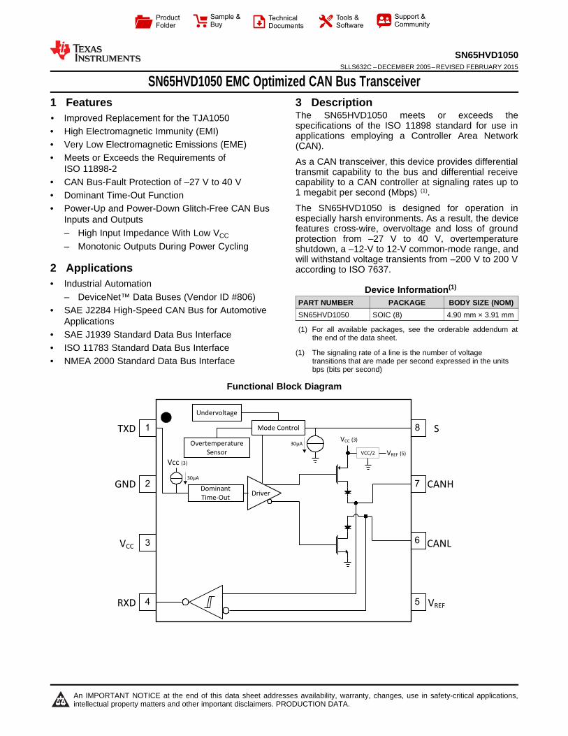
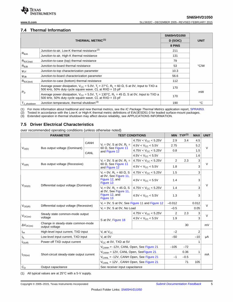
CANH 1 2 3 4 8 7 6 5 TXD GND V CC RXD S CANL V REF Mode Control Overtemperature Sensor Dominant Time-Out 30μA 30μA V CC (3) V REF (5) Driver Vcc (3) Undervoltage VCC/2 Product Folder Sample & Buy Technical Documents Tools & Software Support & Community SN65HVD1050 SLLS632C – DECEMBER 2005 – REVISED FEBRUARY 2015 SN65HVD1050 EMC Optimized CAN Bus Transceiver 1 Features 3 Description The SN65HVD1050 meets or exceeds the 1• Improved Replacement for the TJA1050 specifications of the ISO 11898 standard for use in • High Electromagnetic Immunity (EMI) applications employing a Controller Area Network • Very Low Electromagnetic Emissions (EME) (CAN). • Meets or Exceeds the Requirements of As a CAN transceiver, this device provides differential ISO 11898-2 transmit capability to the bus and differential receive • CAN Bus-Fault Protection of –27 V to 40 V capability to a CAN controller at signaling rates up to 1 megabit per second (Mbps) (1) . • Dominant Time-Out Function The SN65HVD1050 is designed for operation in • Power-Up and Power-Down Glitch-Free CAN Bus especially harsh environments. As a result, the device Inputs and Outputs features cross-wire, overvoltage and loss of ground – High Input Impedance With Low V CC protection from –27 V to 40 V, overtemperature – Monotonic Outputs During Power Cycling shutdown, a –12-V to 12-V common-mode range, and will withstand voltage transients from –200 V to 200 V 2 Applications according to ISO 7637. • Industrial Automation Device Information (1) – DeviceNet™ Data Buses (Vendor ID #806) PART NUMBER PACKAGE BODY SIZE (NOM) • SAE J2284 High-Speed CAN Bus for Automotive SN65HVD1050 SOIC (8) 4.90 mm × 3.91 mm Applications (1) For all available packages, see the orderable addendum at • SAE J1939 Standard Data Bus Interface the end of the data sheet. • ISO 11783 Standard Data Bus Interface (1) The signaling rate of a line is the number of voltage transitions that are made per second expressed in the units • NMEA 2000 Standard Data Bus Interface bps (bits per second) Functional Block Diagram 1 An IMPORTANT NOTICE at the end of this data sheet addresses availability, warranty, changes, use in safety-critical applications, intellectual property matters and other important disclaimers. PRODUCTION DATA.
Transcript of SLLS632C –DECEMBER 2005–REVISED FEBRUARY … · SN65HVD1050 SLLS632C–DECEMBER 2005–REVISED...
CANH
1
2
3
4
8
7
6
5
TXD
GND
VCC
RXD
S
CANL
VREF
Mode Control
Overtemperature
Sensor
Dominant
Time-Out
30µA
30µAVCC (3)
VREF (5)
Driver
Vcc (3)
Undervoltage
VCC/2
Product
Folder
Sample &Buy
Technical
Documents
Tools &
Software
Support &Community
SN65HVD1050SLLS632C –DECEMBER 2005–REVISED FEBRUARY 2015
SN65HVD1050 EMC Optimized CAN Bus Transceiver1 Features 3 Description
The SN65HVD1050 meets or exceeds the1• Improved Replacement for the TJA1050
specifications of the ISO 11898 standard for use in• High Electromagnetic Immunity (EMI) applications employing a Controller Area Network• Very Low Electromagnetic Emissions (EME) (CAN).• Meets or Exceeds the Requirements of As a CAN transceiver, this device provides differential
ISO 11898-2 transmit capability to the bus and differential receive• CAN Bus-Fault Protection of –27 V to 40 V capability to a CAN controller at signaling rates up to
1 megabit per second (Mbps) (1).• Dominant Time-Out FunctionThe SN65HVD1050 is designed for operation in• Power-Up and Power-Down Glitch-Free CAN Busespecially harsh environments. As a result, the deviceInputs and Outputsfeatures cross-wire, overvoltage and loss of ground– High Input Impedance With Low VCC protection from –27 V to 40 V, overtemperature
– Monotonic Outputs During Power Cycling shutdown, a –12-V to 12-V common-mode range, andwill withstand voltage transients from –200 V to 200 V
2 Applications according to ISO 7637.• Industrial Automation Device Information(1)
– DeviceNet™ Data Buses (Vendor ID #806) PART NUMBER PACKAGE BODY SIZE (NOM)• SAE J2284 High-Speed CAN Bus for Automotive SN65HVD1050 SOIC (8) 4.90 mm × 3.91 mm
Applications(1) For all available packages, see the orderable addendum at• SAE J1939 Standard Data Bus Interface the end of the data sheet.
• ISO 11783 Standard Data Bus Interface (1) The signaling rate of a line is the number of voltagetransitions that are made per second expressed in the units• NMEA 2000 Standard Data Bus Interfacebps (bits per second)
Functional Block Diagram
1
An IMPORTANT NOTICE at the end of this data sheet addresses availability, warranty, changes, use in safety-critical applications,intellectual property matters and other important disclaimers. PRODUCTION DATA.
SN65HVD1050SLLS632C –DECEMBER 2005–REVISED FEBRUARY 2015 www.ti.com
Table of Contents1 Features .................................................................. 1 8 Parameter Measurement Information ................ 102 Applications ........................................................... 1 9 Detailed Description ............................................ 14
9.1 Overview ................................................................. 143 Description ............................................................. 19.2 Functional Block Diagram ....................................... 144 Revision History..................................................... 29.3 Feature Description................................................. 145 Description (Continued) ........................................ 39.4 Device Functional Modes........................................ 156 Pin Configuration and Functions ......................... 3
10 Application and Implementation........................ 187 Specifications......................................................... 410.1 Application Information.......................................... 187.1 Absolute Maximum Ratings ...................................... 410.2 Typical Application ................................................ 197.2 ESD Ratings.............................................................. 410.3 System Example ................................................... 227.3 Recommended Operating Conditions....................... 4
11 Power Supply Recommendations ..................... 247.4 Thermal Information .................................................. 512 Layout................................................................... 247.5 Driver Electrical Characteristics ................................ 5
12.1 Layout Guidelines ................................................. 247.6 Receiver Electrical Characteristics ........................... 612.2 Layout Example .................................................... 257.7 Device Switching Characteristics.............................. 6
13 Device and Documentation Support ................. 267.8 Driver Switching Characteristics ............................... 613.1 Trademarks ........................................................... 267.9 Receiver Switching Characteristics........................... 713.2 Electrostatic Discharge Caution............................ 267.10 Supply Current ........................................................ 713.3 Glossary ................................................................ 267.11 S-Pin Characteristics............................................... 7
7.12 VREF-Pin Characteristics ....................................... 7 14 Mechanical, Packaging, and OrderableInformation ........................................................... 267.13 Typical Characteristics ............................................ 8
4 Revision HistoryNOTE: Page numbers for previous revisions may differ from page numbers in the current version.
Changes from Revision B (March 2010) to Revision C Page
• Added Pin Configuration and Functions section, ESD Ratings table, Feature Description section, Device FunctionalModes, Application and Implementation section, Power Supply Recommendations section, Layout section, Deviceand Documentation Support section, and Mechanical, Packaging, and Orderable Information section .............................. 1
Changes from Revision A (May 2007) to Revision B Page
• Deleted The device is also qualified for use in ISO 11898-2 automotive applications in accordance with AEC-Q100."and footnote, "The device is available with Q100 qualification as the SN65HVD1050Q."..................................................... 1
• Changed VCC min/max range from 4.75-5.25V to 4.5-5.5V.................................................................................................... 4• Changed VIH max from 5.25V to 5.5V .................................................................................................................................... 4• Added rows for various parameters showing parameters with VCC ±5% and ±10%.............................................................. 4• Added Signaling Rate spec, min 20kbps................................................................................................................................ 4• Changed VIH min from 2 to 2.1V............................................................................................................................................. 4• Changed Bus output voltage (Dominant) CANH 4.5V < VCC < 5.5V from 4.75 to 5.2 ........................................................... 5
2 Submit Documentation Feedback Copyright © 2005–2015, Texas Instruments Incorporated
Product Folder Links: SN65HVD1050
1
2
3
4
8
7
6
5
TXDGNDVCC
RXD
SCANHCANLVref
SN65HVD1050
SN65HVD1050www.ti.com SLLS632C –DECEMBER 2005–REVISED FEBRUARY 2015
5 Description (Continued)Pin 8 provides for two different modes of operation: high-speed or silent mode. The high-speed mode ofoperation is selected by connecting S (pin 8) to ground.
If a high logic level is applied to the S pin of the SN65HVD1050, the device enters a listen-only silent modeduring which the driver is switched off while the receiver remains fully functional.
In silent mode, all bus activity is passed by the receiver output to the local protocol controller. When datatransmission is required, the local protocol controller reverses this low-current silent mode by placing a logic-lowon the S pin to resume full operation.
A dominant time-out circuit in the SN65HVD1050 prevents the driver from blocking network communication witha hardware or software failure. The time-out circuit is triggered by a falling edge on TXD (pin 1). If no rising edgeis seen before the time-out constant of the circuit expires, the driver is disabled. The circuit is then reset by thenext rising edge on TXD.
Vref (pin 5) is available as a VCC/2 voltage reference to stabilize the output common mode voltage point.
The SN65HVD1050 is characterized for operation from –40°C to 125°C.
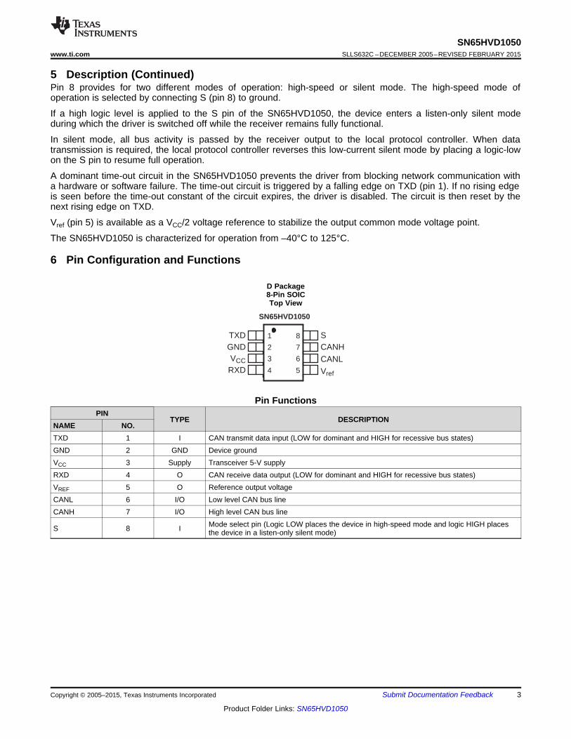
6 Pin Configuration and Functions
D Package8-Pin SOICTop View
Pin FunctionsPIN
TYPE DESCRIPTIONNAME NO.TXD 1 I CAN transmit data input (LOW for dominant and HIGH for recessive bus states)GND 2 GND Device groundVCC 3 Supply Transceiver 5-V supplyRXD 4 O CAN receive data output (LOW for dominant and HIGH for recessive bus states)VREF 5 O Reference output voltageCANL 6 I/O Low level CAN bus lineCANH 7 I/O High level CAN bus line
Mode select pin (Logic LOW places the device in high-speed mode and logic HIGH placesS 8 I the device in a listen-only silent mode)
Copyright © 2005–2015, Texas Instruments Incorporated Submit Documentation Feedback 3
Product Folder Links: SN65HVD1050
SN65HVD1050SLLS632C –DECEMBER 2005–REVISED FEBRUARY 2015 www.ti.com
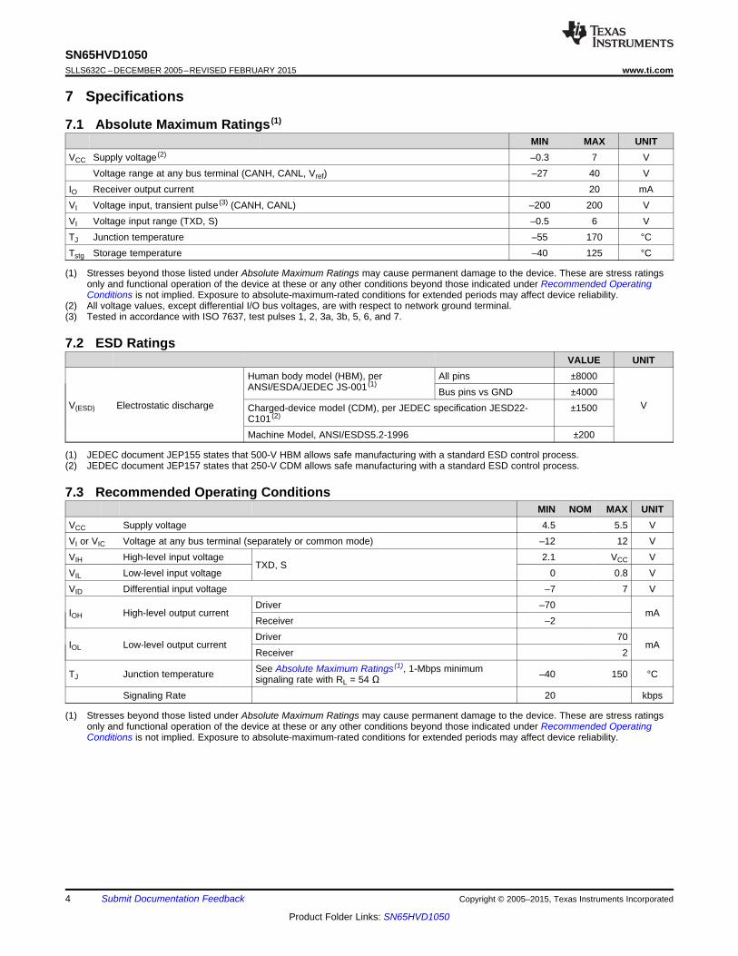
7 Specifications
7.1 Absolute Maximum Ratings (1)
MIN MAX UNITVCC Supply voltage (2) –0.3 7 V
Voltage range at any bus terminal (CANH, CANL, Vref) –27 40 VIO Receiver output current 20 mAVI Voltage input, transient pulse (3) (CANH, CANL) –200 200 VVI Voltage input range (TXD, S) –0.5 6 VTJ Junction temperature –55 170 °CTstg Storage temperature –40 125 °C
(1) Stresses beyond those listed under Absolute Maximum Ratings may cause permanent damage to the device. These are stress ratingsonly and functional operation of the device at these or any other conditions beyond those indicated under Recommended OperatingConditions is not implied. Exposure to absolute-maximum-rated conditions for extended periods may affect device reliability.
(2) All voltage values, except differential I/O bus voltages, are with respect to network ground terminal.(3) Tested in accordance with ISO 7637, test pulses 1, 2, 3a, 3b, 5, 6, and 7.
7.2 ESD RatingsVALUE UNIT
Human body model (HBM), per All pins ±8000ANSI/ESDA/JEDEC JS-001 (1)
Bus pins vs GND ±4000V(ESD) Electrostatic discharge VCharged-device model (CDM), per JEDEC specification JESD22- ±1500
C101 (2)
Machine Model, ANSI/ESDS5.2-1996 ±200
(1) JEDEC document JEP155 states that 500-V HBM allows safe manufacturing with a standard ESD control process.(2) JEDEC document JEP157 states that 250-V CDM allows safe manufacturing with a standard ESD control process.
7.3 Recommended Operating ConditionsMIN NOM MAX UNIT
VCC Supply voltage 4.5 5.5 VVI or VIC Voltage at any bus terminal (separately or common mode) –12 12 VVIH High-level input voltage 2.1 VCC V
TXD, SVIL Low-level input voltage 0 0.8 VVID Differential input voltage –7 7 V
Driver –70IOH High-level output current mA
Receiver –2Driver 70
IOL Low-level output current mAReceiver 2See Absolute Maximum Ratings (1), 1-Mbps minimumTJ Junction temperature –40 150 °Csignaling rate with RL = 54 Ω
Signaling Rate 20 kbps
(1) Stresses beyond those listed under Absolute Maximum Ratings may cause permanent damage to the device. These are stress ratingsonly and functional operation of the device at these or any other conditions beyond those indicated under Recommended OperatingConditions is not implied. Exposure to absolute-maximum-rated conditions for extended periods may affect device reliability.
4 Submit Documentation Feedback Copyright © 2005–2015, Texas Instruments Incorporated
Product Folder Links: SN65HVD1050
SN65HVD1050www.ti.com SLLS632C –DECEMBER 2005–REVISED FEBRUARY 2015
7.4 Thermal InformationSN65HVD1050
THERMAL METRIC (1) D (SOIC) UNIT8 PINS
Junction-to-air, Low-K thermal resistance (2) 211RθJA Junction-to-air, High-K thermal resistance 131RθJC(top) Junction-to-case (top) thermal resistance 79RθJB Junction-to-board thermal resistance 53 °C/WψJT Junction-to-top characterization parameter 10.3ψJB Junction-to-board characterization parameter 56.6RθJC(bot) Junction-to-case (bottom) thermal resistance 112
Average power dissipation, VCC = 5.0V, Tj = 27°C, RL = 60 Ω, S at 0V, Input to TXD a 170500 kHz, 50% duty cycle square wave. CL at RXD = 15 pFPD mW
Average power dissipation, VCC = 5.5V, Tj = 130°C, RL = 45 Ω, S at 0V, Input to TXD a 170500 kHz, 50% duty cycle square wave. CL at RXD = 15 pFTJ_shutdown Junction temperature, thermal shutdown (3) 190 °C
(1) For more information about traditional and new thermal metrics, see the IC Package Thermal Metrics application report, SPRA953.(2) Tested in accordance with the Low-K or High-K thermal metric definitions of EIA/JESD51-3 for leaded surface-mount packages.(3) Extended operation in thermal shutdown may affect device reliability, see APPLICATIONS INFORMATION.
7.5 Driver Electrical Characteristicsover recommended operating conditiions (unless otherwise noted)
PARAMETER TEST CONDITIONS MIN TYP (1) MAX UNIT4.75V < VCC < 5.25V 2.9 3.4 4.5
CANH VI = 0V, S at 0V, RL = 4.5V < VCC < 5.5V 2.75 5.2VO(D) Bus output voltage (Dominant) 60 Ω, See Figure 11 V
4.75V < VCC < 5.25V 0.8 1.5and Figure 12CANL4.5V < VCC < 5.5V 1.6
VI = 3V, S at 0V, RL = 4.75V < VCC < 5.25V 2 2.3 3VO(R) Bus output voltage (Recessive) 60 Ω, See Figure 11 V
4.5V < VCC < 5.5V 1.8 3and Figure 12VI = 0V, RL = 60 Ω, S 4.75V < VCC < 5.25V 1.5 3at 0V, See Figure 11,Figure 12, and 4.5V < VCC < 5.5V 1.4 3Figure 13
VOD(D) Differential output voltage (Dominant) VVI = 0V, RL = 45 Ω, S 4.75V < VCC < 5.25V 1.4 3at 0V, See Figure 11,Figure 12, and 4.5V < VCC < 5.5V 1.3 3Figure 13VI = 3V, S at 0V, See Figure 11 and Figure 12 –0.012 0.012
VOD(R) Differential output voltage (Recessive) VVI = 3V, S at 0V, No Load –0.5 0.05
4.75V < VCC < 5.25V 2 2.3 3Steady state common-mode outputVOC(ss) Vvoltage 4.5V < VCC < 5.5V 1.9 3S at 0V, Figure 18Change in steady-state common-modeΔVOC(ss) 30 mVoutput voltage
IIH High-level input current, TXD input VI at VCC –2 2IIL Low-level input current, TXD input VI at 0V –50 –10 μAIO(off) Power-off TXD output current VCC at 0V, TXD at 5V 1
VCANH = -12V, CANL Open, See Figure 21 –105 –72VCANH = 12V, CANL Open, SeeFigure 21 0.36 1
IOS(ss) Short-circuit steady-state output current mAVCANL = -12V, CANH Open, See Figure 21 –1 –0.5VCANL = 12V , CANH Open, See Figure 21 71 105
CO Output capacitance See receiver input capacitance
(1) All typical values are at 25°C with a 5-V supply.
Copyright © 2005–2015, Texas Instruments Incorporated Submit Documentation Feedback 5
Product Folder Links: SN65HVD1050
SN65HVD1050SLLS632C –DECEMBER 2005–REVISED FEBRUARY 2015 www.ti.com
7.6 Receiver Electrical Characteristicsover recommended operating conditions (unless otherwise noted)
PARAMETER TEST CONDITIONS MIN TYP (1) MAX UNITVIT+ Positive-going input threshold voltage 800 900
S at 0V, See Table 1VIT– Negative-going input threshold voltage 500 650 mVVhys Hysteresis voltage (VIT+ – VIT–) 100 125
4.75V < VCC < 5.25V 4 4.6IO = –2 mA, SeeVOH High-level output voltage VFigure 16 4.5V < VCC < 5.5V 3.8VOL Low-level output voltage IO = 2 mA, See Figure 16 0.2 0.4 V
CANH or CANL = 5V,II(off) Power-off bus input current Other pin at 0V, 165 250 μA
VCC at 0V, TXD at 0VIO(off) Power-off RXD leakage current VCC at 0V, RXD at 5V 20 μA
Input capacitance to ground, (CANH or TXD at 3V,CI 13CANL) VI = 0.4 sin (4E6πt) + 2.5V pFCID Differential input capacitance TXD at 3V, VI = 0.4 sin (4E6πt) 5RID Differential input resistance 30 80
TXD at 3V, S at 0V kΩRIN Input resistance, (CANH or CANL) 15 30 40
Input resistance matchingRI(m) V(CANH) = V(CANL) –3% 0% 3%[1 – (RIN (CANH) / RIN (CANL))] x 100%
(1) All typical values are at 25°C with a 5-V supply.
7.7 Device Switching Characteristicsover operating free-air temperature range (unless otherwise noted)
PARAMETER TEST CONDITIONS MIN TYP MAX UNIT4.75V < VCC < 5.25V 90 190Total loop delay, driver input to receiver output,td(LOOP1) recessive to dominant 4.5V < VCC < 5.5V 85 195Figure 19, S at ns0V 4.75V < VCC < 5.25V 90 190Total loop delay, driver input to receiver output,td(LOOP2) dominant to recessive 4.5V < VCC < 5.5V 85 195
7.8 Driver Switching Characteristicsover recommended operating conditions (unless otherwise noted)
PARAMETER TEST CONDITIONS MIN TYP MAX UNITtPLH Propagation delay time, low-to-high-level output 25 65 120tPHL Propagation delay time, high-to-low-level output 25 45 90
S at 0V, See Figure 14 nstr Differential output signal rise time 25tf Differential output signal fall time 50ten Enable time from silent mode to dominant See Figure 17 1 μs
4.75V < VCC < 5.25V 300 450 700↓VI, Seet(dom) Dominant time-out μsFigure 20 4.5V < VCC < 5.5V 280 700
6 Submit Documentation Feedback Copyright © 2005–2015, Texas Instruments Incorporated
Product Folder Links: SN65HVD1050
SN65HVD1050www.ti.com SLLS632C –DECEMBER 2005–REVISED FEBRUARY 2015
7.9 Receiver Switching Characteristicsover recommended operating conditions (unless otherwise noted)
PARAMETER TEST CONDITIONS MIN TYP MAX UNITtPLH Propagation delay time, low-to-high-level output 4.75V < VCC < 5.25V 60 100 130
4.5V < VCC < 5.5V 60 135tPHL Propagation delay time, high-to-low-level output 4.75V < VCC < 5.25V 45 70 90S at 0V or VCC, See nsFigure 16 4.5V < VCC < 5.5V 45 95tr Output signal rise time 8tf Output signal fall time 8
7.10 Supply Currentover recommended operating conditions (unless otherwise noted)
PARAMETER TEST CONDITIONS MIN TYP MAX UNITSilent mode S at VCC, VI = VCC 6 10
4.75V < VCC < 5.25V 50 70ICC 5-V Supply current Dominant VI = 0V, 60 Ω Load, S at 0V mA
4.5V < VCC < 5.5V 75Recessive VI = VCC, No Load, S at 0V 6 10
7.11 S-Pin Characteristicsover recommended operating conditiions (unless otherwise noted)
PARAMETER TEST CONDITIONS MIN TYP MAX UNITIIH High level input current S at 2V 20 40 70
μAIIL Low level input current S at 0.8V 5 20 30
7.12 VREF-Pin Characteristicsover operating free-air temperature range (unless otherwise noted)
PARAMETER TEST CONDITIONS MIN TYP MAX UNITVREF Reference output voltage –50 μA < IO < 50 μA 0.4VCC 0.5VCC 0.6VCC V
Copyright © 2005–2015, Texas Instruments Incorporated Submit Documentation Feedback 7
Product Folder Links: SN65HVD1050
0
0.5
1
1.5
2
2.5
3
−40 0 25 70 125
S at 0 V,RL = 60 ,Air Flow at 7 cf/m,TXD Input is a 125 kHz1% Duty Cycle Pulse
TA − Free-Air Temperature − °C
VCC = 5 V
VCC = 4.75 V
VCC = 5.25 V
Do
min
an
t D
river
Dif
fere
nti
al
Ou
tpu
t Vo
ltag
e−
V
Ω
-0
-10
-20
-30
-40
-50
-60
-70
-80
0 1 2 3 4 5
TA = 25 C,VCC = 5 V,S at 0 V,TXD Input is a 125 kHz1% Duty Cycle Pulse
I OH
−H
igh
-Level O
utp
ut
Cu
rren
t−
mA
VOCANH − High-Level Output Voltage − V
0
5
10
15
20
25
30
35
40
45
50
200 400 500 600 800 1000
Signaling Rate − kbps
I CC
−R
MS
Su
pp
ly C
urr
en
t−
mA
TA = 25°C,VCC = 5 V,S at 0 V,RL = 60 ,RXD = 15 pF
Ω
−10
0
10
20
30
40
50
60
70
80
90
0 1 2 3 4 5
TA = 25°C,VCC = 5 V,S at 0 V,TXD Input is a 125 kHz1% Duty Cycle Pulse
I OL
−L
ow
-Level
Ou
tpu
t C
urr
en
t−
mA
VOCANL − Low-Level Output Voltage − V
140
145
150
155
160
165
170
−40 0 25 70 125
VCC = 5.25 V
−D
om
inan
t-to
-Recessiv
e L
oo
p Tim
e−
ns
tL
OO
P2
TA − Free-Air Temperature −°C
VCC = 5 V
VCC = 4.75 V
S at 0 V,
R = 60 ,
C = 100 pF,
Air Flow at 7 cf/m,TXD Input is a 125 kHz,50% Duty Cycle Pulse
L
L
W
120
125
130
135
140
145
150
−40 0 25 70 125
VCC = 4.75 V
VCC = 5 V
VCC = 5.25 V
−R
ecessiv
e-t
o-D
om
inan
t L
oo
p Tim
e−
ns
tL
OO
P1
TA − Free-Air Temperature −°C
S at 0 V,
R = 60 ,
C = 100 pF,
Air Flow at 7 cf/m,TXD Input is a 125 kHz,50% Duty Cycle Pulse
L
L
W
SN65HVD1050SLLS632C –DECEMBER 2005–REVISED FEBRUARY 2015 www.ti.com
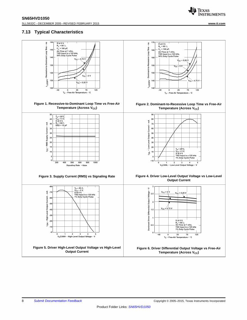
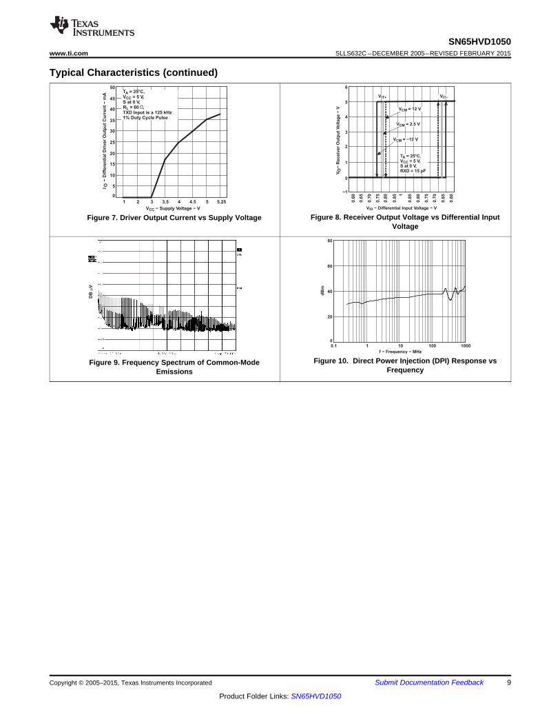
7.13 Typical Characteristics
Figure 1. Recessive-to-Dominant Loop Time vs Free-Air Figure 2. Dominant-to-Recessive Loop Time vs Free-AirTemperature (Across VCC) Temperature (Across VCC)
Figure 4. Driver Low-Level Output Voltage vs Low-LevelFigure 3. Supply Current (RMS) vs Signaling RateOutput Current
Figure 5. Driver High-Level Output Voltage vs High-Level Figure 6. Driver Differential Output Voltage vs Free-AirOutput Current Temperature (Across VCC)
8 Submit Documentation Feedback Copyright © 2005–2015, Texas Instruments Incorporated
Product Folder Links: SN65HVD1050
DB
Vm
0
20
40
60
80
0.1 1 10 100 1000
f − Frequency − MHz
dB
m
0
5
10
15
20
25
30
35
40
45
50
1 2 3 3.5 4 4.5 5 5.25
TA = 25°C,VCC = 5 V,S at 0 V,RL = 60 ,TXD Input is a 125 kHz1% Duty Cycle Pulse
I O−
Dif
fere
nti
al
Dri
ver
Ou
tpu
t C
urr
en
t−
mA
VCC − Supply Voltage − V
Ω
−1
0
1
2
3
4
5
6
0.6
0
0.6
5
0.7
0
0.7
5
0.8
0
0.8
5 1
0.8
5
0.8
0
0.7
5
0.7
0
0.6
5
0.6
0
VIT+ VIT−
VCM = 12 V
VCM = 2.5 V
VCM = −12 V
TA = 25°C,VCC = 5 V,S at 0 V,RXD = 15 pF
−R
eceiv
er
Ou
tpu
t Vo
ltag
e−
VV
O
VID − Differential Input Voltage − V
SN65HVD1050www.ti.com SLLS632C –DECEMBER 2005–REVISED FEBRUARY 2015
Typical Characteristics (continued)
Figure 8. Receiver Output Voltage vs Differential InputFigure 7. Driver Output Current vs Supply VoltageVoltage
Figure 10. Direct Power Injection (DPI) Response vsFigure 9. Frequency Spectrum of Common-ModeFrequencyEmissions
Copyright © 2005–2015, Texas Instruments Incorporated Submit Documentation Feedback 9
Product Folder Links: SN65HVD1050
CANH
CANL
VIDVI (CANH) + VI (CANL)
2VIC =
VI (CANH)
VI (CANL)
VO
IO
RXD
S
CANH
CANL
V I
TXD
(See Note A)
90%
10%
0.9 V
tPLH
0.5 V
VCC/2 VCC/2
VCC
0 V
VO(D)
VO(R)
tPHL
tr tf
VI
VO
VO
C = 100 pF
(see Note B)L
R = 60
±1%L W
0 V VOD
+_
CANH
CANL
TXD
S
RL
330 1%
330 1%
−2 V VTEST 7 V
IO(CANH)
VOD
VI
TXD O (CANH)V
O(CANL)V
IO(CANL)
RL
OCV
O(CANH)V O(CANL)V+
2II(S)
VI(S)
+
_
S
II
3.5 V
2.5 V
1.5 V
VO(CANH)
VO(CANL)
Dominant
Recessive
SN65HVD1050SLLS632C –DECEMBER 2005–REVISED FEBRUARY 2015 www.ti.com
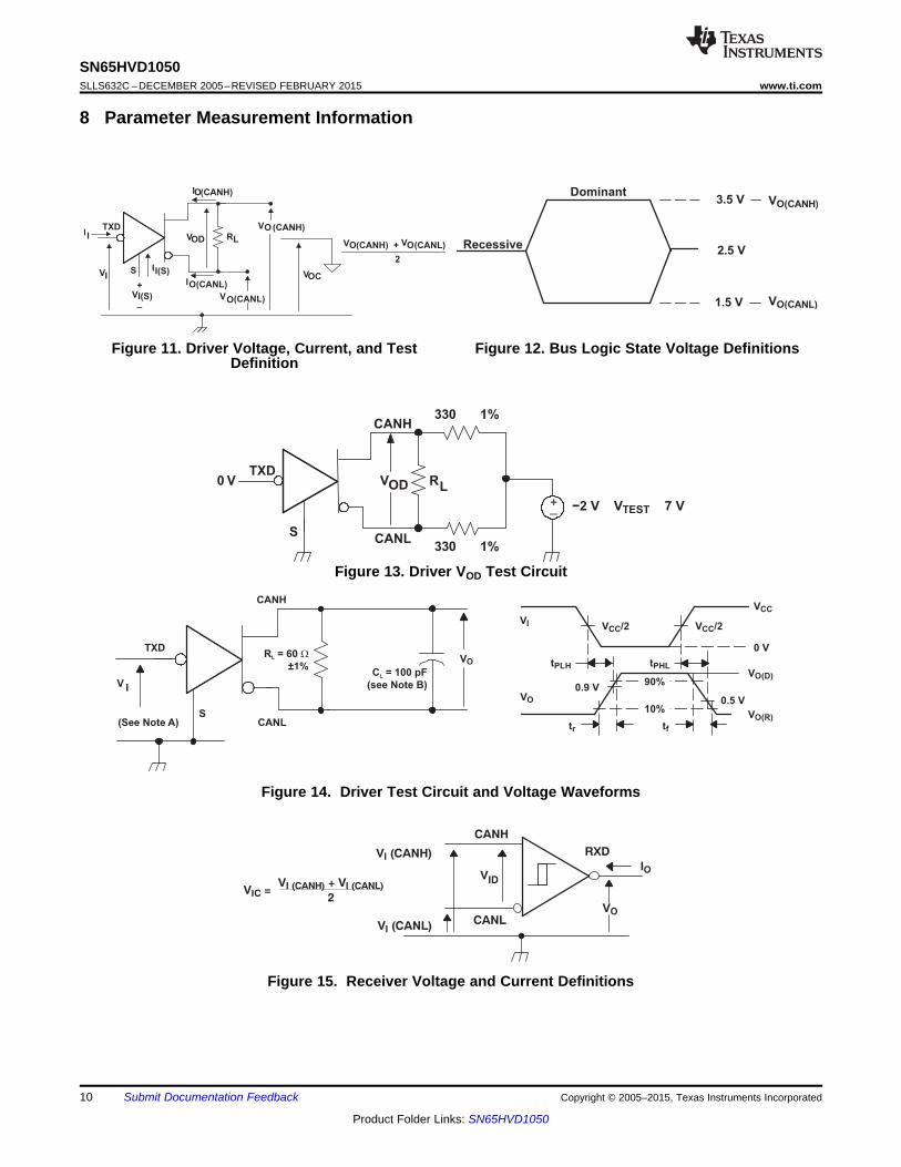
8 Parameter Measurement Information
Figure 11. Driver Voltage, Current, and Test Figure 12. Bus Logic State Voltage DefinitionsDefinition
Figure 13. Driver VOD Test Circuit
Figure 14. Driver Test Circuit and Voltage Waveforms
Figure 15. Receiver Voltage and Current Definitions
10 Submit Documentation Feedback Copyright © 2005–2015, Texas Instruments Incorporated
Product Folder Links: SN65HVD1050
+
_
DUT
TXD
S
RXD
15 pF 20%
VO
VI
0 V CL 60 1%
CANH
CANL
NOTE: CL = 100 pFincludesinstrumentationand fixture capacitancewithin ±20%
50 %
50 %
ten
VCC
0 V
VOH
VOL
VI
VO
NOTE: All VI input pulses are supplied by a generator having thefollowing characteristics: tr or tf ≤ 6 ns, Pulse Repetition Rate(PRR) = 25 kHz, 50% duty cycle
1.5 V
CANH
CANL
RXDV I
(See Note A)S
CL = 15 pF 20%(See Note B)
IO
VO
VI
VO
tPLH
0.7 VCC
2 V 2.4 V
tPHL
0.3 VCC
90%
10%
3.5 V
1.5 V
VOH
VOLtr tf
SN65HVD1050www.ti.com SLLS632C –DECEMBER 2005–REVISED FEBRUARY 2015
Parameter Measurement Information (continued)
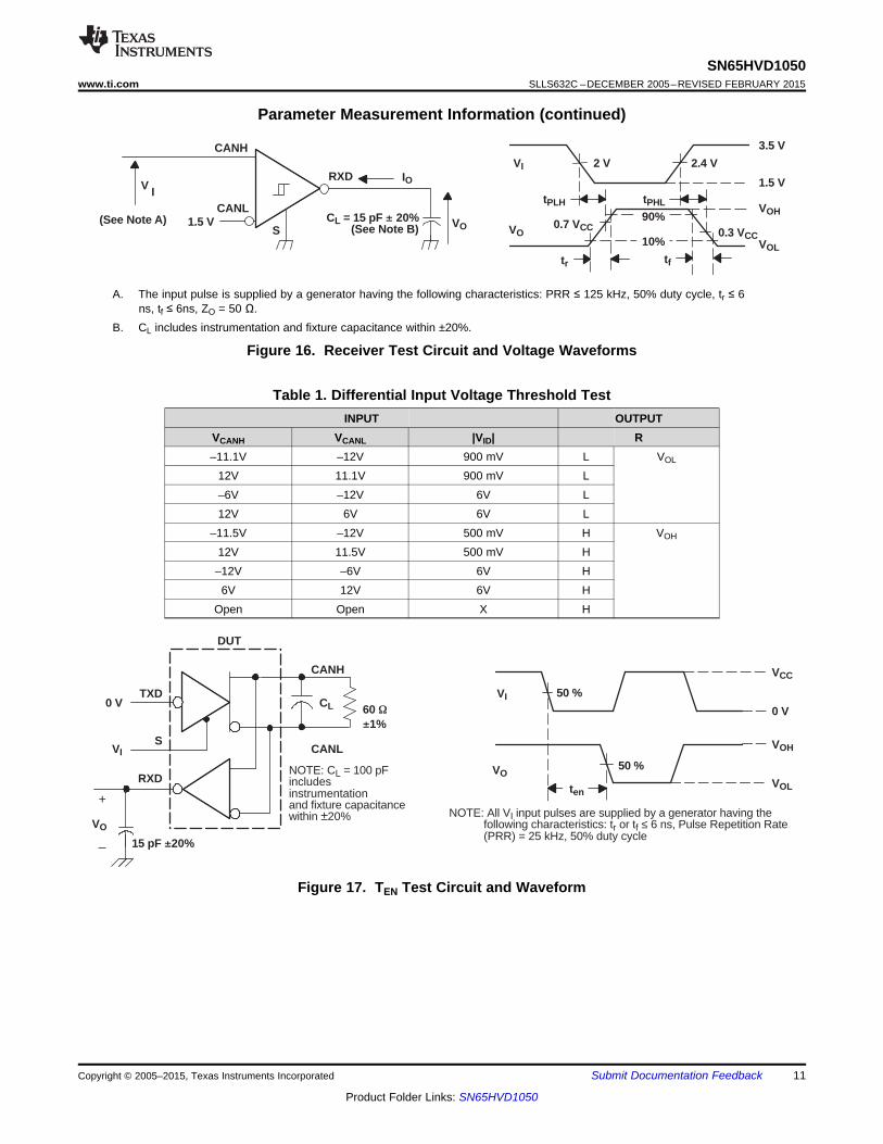
A. The input pulse is supplied by a generator having the following characteristics: PRR ≤ 125 kHz, 50% duty cycle, tr ≤ 6ns, tf ≤ 6ns, ZO = 50 Ω.
B. CL includes instrumentation and fixture capacitance within ±20%.
Figure 16. Receiver Test Circuit and Voltage Waveforms
Table 1. Differential Input Voltage Threshold TestINPUT OUTPUT
VCANH VCANL |VID| R–11.1V –12V 900 mV L VOL
12V 11.1V 900 mV L–6V –12V 6V L12V 6V 6V L
–11.5V –12V 500 mV H VOH
12V 11.5V 500 mV H–12V –6V 6V H6V 12V 6V H
Open Open X H
Figure 17. TEN Test Circuit and Waveform
Copyright © 2005–2015, Texas Instruments Incorporated Submit Documentation Feedback 11
Product Folder Links: SN65HVD1050
SCANH
VI
TXD
(See Note A)
RL = 60 1%
CL(See Note B)
VOD
tdom
VI
900 mVVOD
500 mV
VCC
0 V
VOD(D)
0 V
+
_
DUT
TXD
S
RXD
VI CL
CANH
CANL
NOTE: CL = 100 pFincludes instrumentationand fixture capacitancewithin±20%
VO
50%50%
50%
VCC
0 V
VOH
VOL
TXD Input
RXD Output
tloop2tloop1
15 pF ±20%
60±1%
W
CANH
CANL
TXD
S
VI
47 nF20%
27 1%
27 1%VOC = VO(CANH) + VO(CANL)
2
VOC(SS)
VOC
SN65HVD1050SLLS632C –DECEMBER 2005–REVISED FEBRUARY 2015 www.ti.com
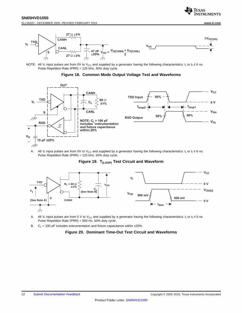
NOTE: All VI input pulses are from 0V to VCC and supplied by a generator having the following characteristics: tr or tf ≤ 6 ns.Pulse Repetition Rate (PRR) = 125 kHz, 50% duty cycle.
Figure 18. Common Mode Output Voltage Test and Waveforms
A. All VI input pulses are from 0V to VCC and supplied by a generator having the following characteristics: tr or tf ≤ 6 ns.Pulse Repetition Rate (PRR) = 125 kHz, 50% duty cycle.
Figure 19. T(LOOP) Test Circuit and Waveform
A. All VI input pulses are from 0 V to VCC and supplied by a generator having the following characteristics: tr or tf ≤ 6 ns.Pulse Repetition Rate (PRR) = 500 Hz, 50% duty cycle.
B. CL = 100 pF includes instrumentation and fixture capacitance within ±20%.
Figure 20. Dominant Time-Out Test Circuit and Waveforms
12 Submit Documentation Feedback Copyright © 2005–2015, Texas Instruments Incorporated
Product Folder Links: SN65HVD1050
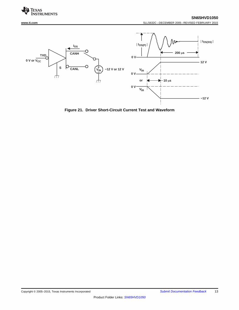
TXD CANH
CANLS Vin
Vin
0 V
0 V
12 V
−12 V
or
0 V0 V or VCC
VIN
IOS
−12 V or 12 V
| IOS(SS) || IOS(P) |
200 s
10 s
SN65HVD1050www.ti.com SLLS632C –DECEMBER 2005–REVISED FEBRUARY 2015
Figure 21. Driver Short-Circuit Current Test and Waveform
Copyright © 2005–2015, Texas Instruments Incorporated Submit Documentation Feedback 13
Product Folder Links: SN65HVD1050
TXD
RXD
S
CANH
CANL
Mode Control
Overtemperature
Sensor
Dominant
Time-Out
30µA
30µAVCC (3)
VREF
Driver
Vcc (3)
Undervoltage
8
7
6
1
4
VCC/25
SN65HVD1050SLLS632C –DECEMBER 2005–REVISED FEBRUARY 2015 www.ti.com
9 Detailed Description
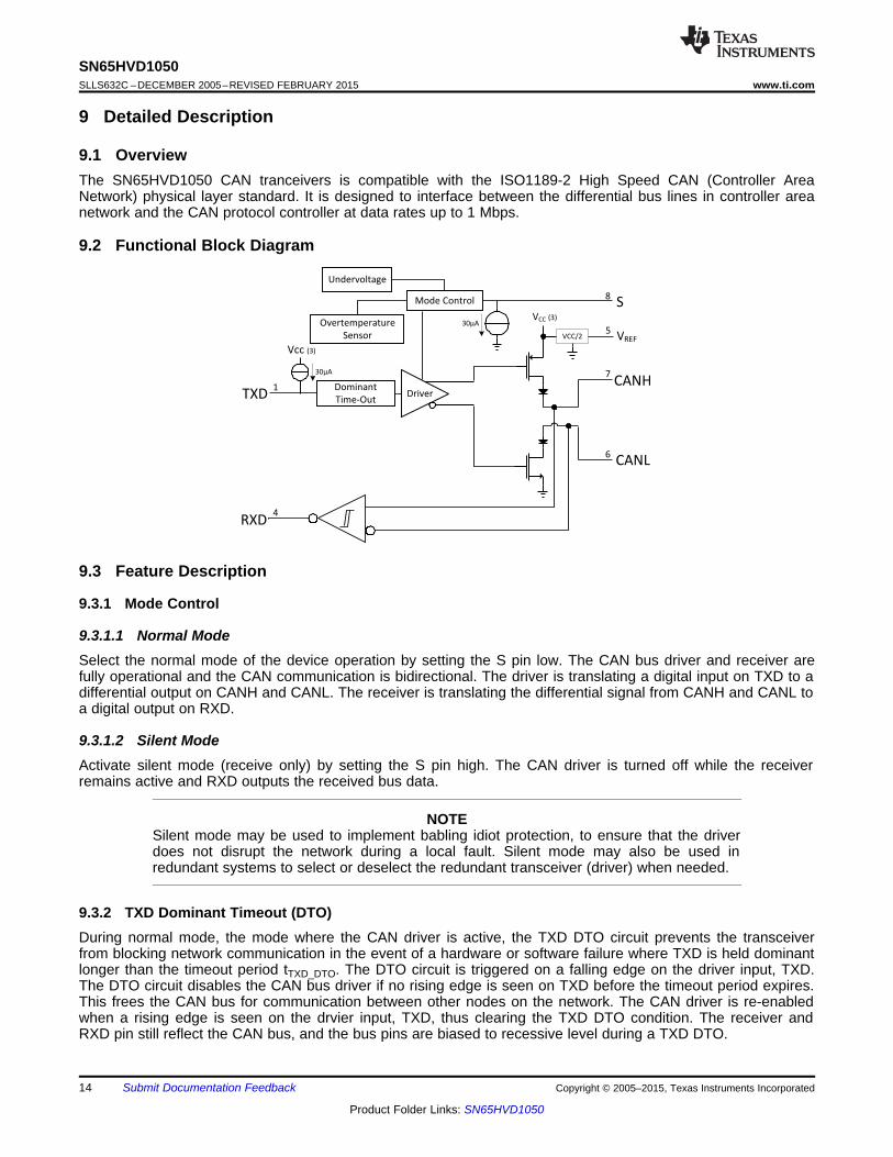
9.1 OverviewThe SN65HVD1050 CAN tranceivers is compatible with the ISO1189-2 High Speed CAN (Controller AreaNetwork) physical layer standard. It is designed to interface between the differential bus lines in controller areanetwork and the CAN protocol controller at data rates up to 1 Mbps.
9.2 Functional Block Diagram
9.3 Feature Description
9.3.1 Mode Control
9.3.1.1 Normal ModeSelect the normal mode of the device operation by setting the S pin low. The CAN bus driver and receiver arefully operational and the CAN communication is bidirectional. The driver is translating a digital input on TXD to adifferential output on CANH and CANL. The receiver is translating the differential signal from CANH and CANL toa digital output on RXD.
9.3.1.2 Silent ModeActivate silent mode (receive only) by setting the S pin high. The CAN driver is turned off while the receiverremains active and RXD outputs the received bus data.
NOTESilent mode may be used to implement babling idiot protection, to ensure that the driverdoes not disrupt the network during a local fault. Silent mode may also be used inredundant systems to select or deselect the redundant transceiver (driver) when needed.
9.3.2 TXD Dominant Timeout (DTO)During normal mode, the mode where the CAN driver is active, the TXD DTO circuit prevents the transceiverfrom blocking network communication in the event of a hardware or software failure where TXD is held dominantlonger than the timeout period tTXD_DTO. The DTO circuit is triggered on a falling edge on the driver input, TXD.The DTO circuit disables the CAN bus driver if no rising edge is seen on TXD before the timeout period expires.This frees the CAN bus for communication between other nodes on the network. The CAN driver is re-enabledwhen a rising edge is seen on the drvier input, TXD, thus clearing the TXD DTO condition. The receiver andRXD pin still reflect the CAN bus, and the bus pins are biased to recessive level during a TXD DTO.
14 Submit Documentation Feedback Copyright © 2005–2015, Texas Instruments Incorporated
Product Folder Links: SN65HVD1050
SN65HVD1050www.ti.com SLLS632C –DECEMBER 2005–REVISED FEBRUARY 2015
Feature Description (continued)
NOTEThe minimum dominant TXD time allowed by the TXD DTO circuit limits the minimumpossible transmitted data rate on the device. The CAN protocol allows a maximum ofeleven successive dominant bits (on TXD) for the worst case, where five successivedominant bits are followed immediately by an error frame. This, along with the tTXD_DTOminimum, limits the minimum data rate. Calculate the minimum transmitted data rateusing: Minimum Data Rate = 11 / tTXD_DTO
9.3.3 Thermal ShutdownThe SN65HVD1050 has a thermal shutdown feature that turns off the driver outputs when the junctiontemperature nears 190°C. This shutdown prevents catastrophic failure from bus shorts, but does not protect thecircuit from possible damage. The user should strive to maintain recommended operating conditions and notexceed absolute-maximum ratings at all times. If an SN65HVD1050 is subjected to many, or long-duration faultsthat can put the device into thermal shutdown, it should be replaced.
9.3.4 VREF
A reference voltage of VCC/2 is available through the VREF output pin. The VREF voltage should be tied to thecommon mode point in a split termination network to help stabilize the output common mode voltage. SeeFigure 27 for more application specific information on properly terminating the CAN bus.
If the VREF output pin is not used it can be left floating.
9.3.5 Operating Temperature RangeThe SN65HVD1050 is characterized for operation from –40°C to 125°C.
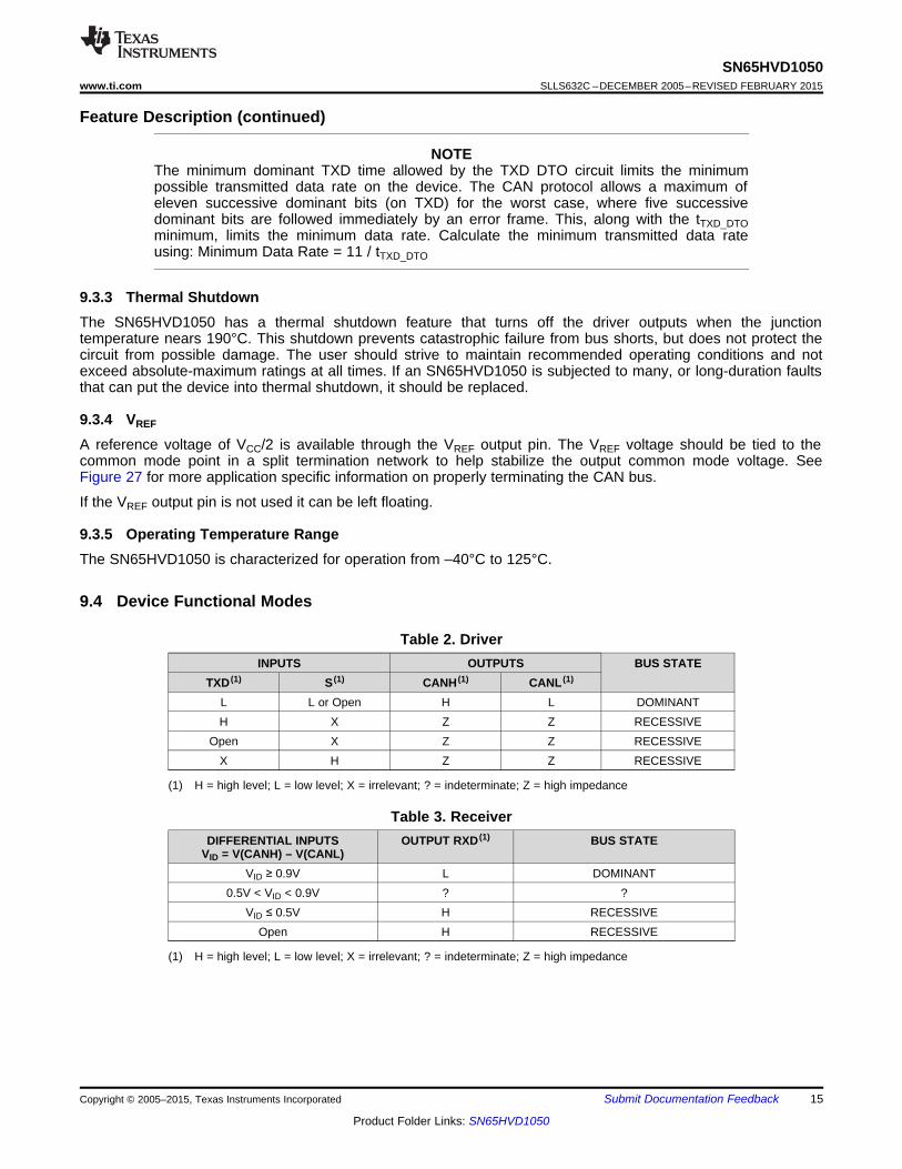
9.4 Device Functional Modes
Table 2. DriverINPUTS OUTPUTS BUS STATE
TXD (1) S (1) CANH (1) CANL (1)
L L or Open H L DOMINANTH X Z Z RECESSIVE
Open X Z Z RECESSIVEX H Z Z RECESSIVE
(1) H = high level; L = low level; X = irrelevant; ? = indeterminate; Z = high impedance
Table 3. ReceiverDIFFERENTIAL INPUTS OUTPUT RXD (1) BUS STATE
VID = V(CANH) – V(CANL)VID ≥ 0.9V L DOMINANT
0.5V < VID < 0.9V ? ?VID ≤ 0.5V H RECESSIVE
Open H RECESSIVE
(1) H = high level; L = low level; X = irrelevant; ? = indeterminate; Z = high impedance
Copyright © 2005–2015, Texas Instruments Incorporated Submit Documentation Feedback 15
Product Folder Links: SN65HVD1050
SN65HVD1050SLLS632C –DECEMBER 2005–REVISED FEBRUARY 2015 www.ti.com
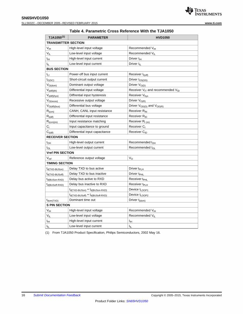
Table 4. Parametric Cross Reference With the TJA1050TJA1050 (1) PARAMETER HVD1050
TRANSMITTER SECTIONVIH High-level input voltage Recommended VIH
VIL Low-level input voltage Recommended VIL
IIH High-level input current Driver IIHIIL Low-level input current Driver IILBUS SECTIONILI Power-off bus input current Receiver II(off)
IO(SC) Short-circuit output current Driver IOS(SS)
VO(dom) Dominant output voltage Driver VO(D)
Vi(dif)(th) Differential input voltage Receiver VIT and recommended VID
Vi(dif)(hys) Diffrential input hysteresis Receiver Vhys
VO(reces) Recessive output voltage Driver VO(R)
VO(dif)(bus) Differential bus voltage Driver VOD(D) and VOD(R)
Ri(cm) CANH, CANL input resistance Receiver RIN
Ri(dif) Differential input resistance Receiver RID
Ri(cm)(m) Input resistance matching Receiver RI (m)
Ci Input capacitance to ground Receiver CI
Ci(dif) Differential input capacitance Receiver CID
RECEIVER SECTIONIOH High-level output current Recommended IOH
IOL Low-level output current Recommended IOL
Vref PIN SECTIONVref Reference output voltage VO
TIMING SECTIONtd(TXD-BUSon) Delay TXD to bus active Driver tPLH
td(TXD-BUSoff) Delay TXD to bus inactive Driver tPHL
td(BUSon-RXD) Delay bus active to RXD Receiver tPHL
td(BUSoff-RXD) Delay bus inactive to RXD Receiver tPLH
td(TXD-BUSon) + td(BUSon-RXD) Device tLOOP1
td(TXD-BUSoff) + td(BUSoff-RXD) Device tLOOP2
tdom(TXD) Dominant time out Driver t(dom)
S PIN SECTIONVIH High-level input voltage Recommended VIH
VIL Low-level input voltage Recommended VIL
IIH High-level input current IIHIIL Low-level input current IIL
(1) From TJA1050 Product Specification, Philips Semiconductors, 2002 May 16.
16 Submit Documentation Feedback Copyright © 2005–2015, Texas Instruments Incorporated
Product Folder Links: SN65HVD1050
VccRXD Output
Output
Vcc
Vref Output
Output
S Input
Vcc
6 V
Input
Vcc
CANL
CANH and CANL Outputs
CANH Input
Vcc
Input
TXD Input
Vcc
Input
CANL Input
Vcc
Input
CANH
4.3 kW 25 W
10 kW
20 kW
10 kW
10 kW
10 kW
20 kW
40 V40 V
4.3 kW
40 kW
40 V
40 V
2 kW
2 kW
40 V
6 V6 V
SN65HVD1050www.ti.com SLLS632C –DECEMBER 2005–REVISED FEBRUARY 2015
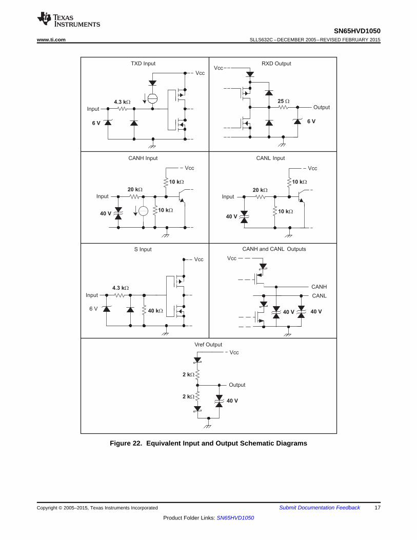
Figure 22. Equivalent Input and Output Schematic Diagrams
Copyright © 2005–2015, Texas Instruments Incorporated Submit Documentation Feedback 17
Product Folder Links: SN65HVD1050
RXD
CANH
CANL
VCC/2
Recessive
Logic H
Dominant
Logic L
Recessive
Logic H
Time, t
Ty
pic
al
Bu
sV
olt
ag
e(V
)
CANL
CANH
Vdiff(D)
Vdiff(R)
12
34
SN65HVD1050SLLS632C –DECEMBER 2005–REVISED FEBRUARY 2015 www.ti.com
10 Application and Implementation
NOTEInformation in the following applications sections is not part of the TI componentspecification, and TI does not warrant its accuracy or completeness. TI’s customers areresponsible for determining suitability of components for their purposes. Customers shouldvalidate and test their design implementation to confirm system functionality.
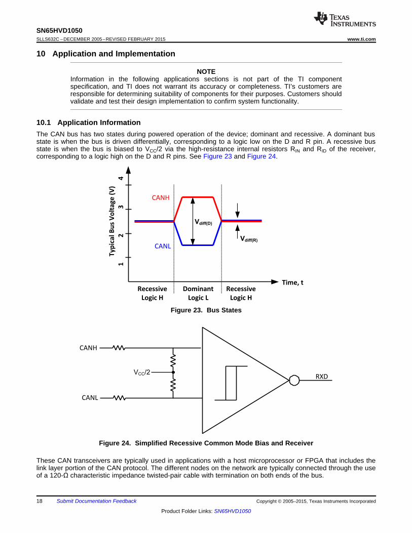
10.1 Application InformationThe CAN bus has two states during powered operation of the device; dominant and recessive. A dominant busstate is when the bus is driven differentially, corresponding to a logic low on the D and R pin. A recessive busstate is when the bus is biased to VCC/2 via the high-resistance internal resistors RIN and RID of the receiver,corresponding to a logic high on the D and R pins. See Figure 23 and Figure 24.
Figure 23. Bus States
Figure 24. Simplified Recessive Common Mode Bias and Receiver
These CAN transceivers are typically used in applications with a host microprocessor or FPGA that includes thelink layer portion of the CAN protocol. The different nodes on the network are typically connected through the useof a 120-Ω characteristic impedance twisted-pair cable with termination on both ends of the bus.
18 Submit Documentation Feedback Copyright © 2005–2015, Texas Instruments Incorporated
Product Folder Links: SN65HVD1050
MCU or DSP
CAN
Controller
SN65HVD251 CAN
Transceiver
Node 1
MCU or DSP
CAN
Controller
SN65HVD1050 CAN
Transceiver
Node 2
MCU or DSP
CAN
Controller
SN65HVD233 CAN
Transceiver
Node 3
MCU or DSP
CAN
Controller
SN65HVD257 CAN
Transceiver
Node n(with termination)
RTERM
RTERM
5-V Voltage
Regulator
(such as TPS76350)
VIN
VIN VOUT
5V MCU
RXD
TXD
S
VCC
VREF (5)
TXD (1)
RXD (4)
GND (2)
3
CANH (7)
CANL (6)
S (8)
Optional:
Terminating
Node
SN65HVD1050www.ti.com SLLS632C –DECEMBER 2005–REVISED FEBRUARY 2015
10.2 Typical Application
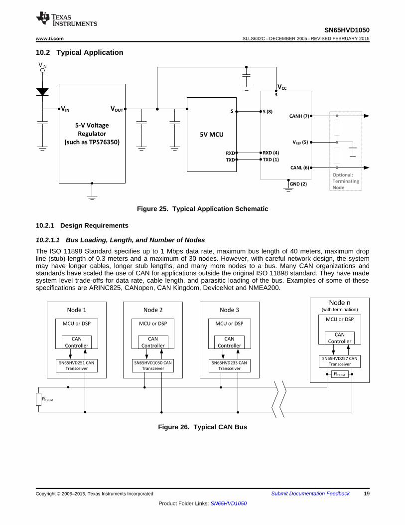
Figure 25. Typical Application Schematic
10.2.1 Design Requirements
10.2.1.1 Bus Loading, Length, and Number of NodesThe ISO 11898 Standard specifies up to 1 Mbps data rate, maximum bus length of 40 meters, maximum dropline (stub) length of 0.3 meters and a maximum of 30 nodes. However, with careful network design, the systemmay have longer cables, longer stub lengths, and many more nodes to a bus. Many CAN organizations andstandards have scaled the use of CAN for applications outside the original ISO 11898 standard. They have madesystem level trade-offs for data rate, cable length, and parasitic loading of the bus. Examples of some of thesespecifications are ARINC825, CANopen, CAN Kingdom, DeviceNet and NMEA200.
Figure 26. Typical CAN Bus
Copyright © 2005–2015, Texas Instruments Incorporated Submit Documentation Feedback 19
Product Folder Links: SN65HVD1050
CAN
TransceiverRTERM
Standard Termination
CANL
CANH
CAN
Transceiver
CANL
CANH
RTERM/2
RTERM/2
Split Termination
SN65HVD1050SLLS632C –DECEMBER 2005–REVISED FEBRUARY 2015 www.ti.com
Typical Application (continued)A high number of nodes requires a transceiver with high input impedance and wide common mode range suchas the SN65HVD1050 CAN transceiver. ISO 11898-2 specifies the driver differential output with a 60-Ω load (two120-Ω termination resistors in parallel) and the differential output must be greater than 1.5 V. The SN65HVD1050device is specified to meet the 1.5-V requirement with a 60-Ω load, and additionally specified with a differentialoutput voltage minimum of 1.2 V across a common mode range of –2 V to 7 V via a 330-Ω coupling network.This network represents the bus loading of 90 SN65HVD1050 transceivers based on their minimum differentialinput resistance of 30 kΩ. Therefore, the SN65HVD1050 supports up to 90 transceivers on a single bus segmentwith margin to the 1.2-V minimum differential input voltage requirement at each node.
For CAN network design, margin must be given for signal loss across the system and cabling, parasitic loadings,network imbalances, ground offsets and signal integrity thus a practical maximum number of nodes may belower. Bus length may also be extended beyond the original ISO 11898 standard of 40 meters by careful systemdesign and data rate tradeoffs. For example, CANopen network design guidelines allow the network to be up to1-km with changes in the termination resistance, cabling, less than 64 nodes and significantly lowered data rate.
This flexibility in CAN network design is one of the key strengths of the various extensions and additionalstandards that have been built on the original ISO 11898 CAN standard.
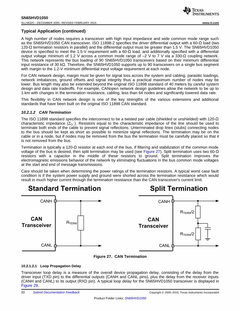
10.2.1.2 CAN TerminationThe ISO 11898 standard specifies the interconnect to be a twisted pair cable (shielded or unshielded) with 120-Ωcharacteristic impedance (ZO ). Resistors equal to the characteristic impedance of the line should be used toterminate both ends of the cable to prevent signal reflections. Unterminated drop lines (stubs) connecting nodesto the bus should be kept as short as possible to minimize signal reflections. The termination may be on thecable or in a node, but if nodes may be removed from the bus the termination must be carefully placed so that itis not removed from the bus.
Termination is typically a 120-Ω resistor at each end of the bus. If filtering and stabilization of the common modevoltage of the bus is desired, then split termination may be used (see Figure 27). Split termination uses two 60-Ωresistors with a capacitor in the middle of these resistors to ground. Split termination improves theelectromagnetic emissions behavior of the network by eliminating fluctuations in the bus common mode voltagesat the start and end of message transmissions.
Care should be taken when determining the power ratings of the termination resistors. A typical worst case faultcondition is if the system power supply and ground were shorted across the termination resistance which wouldresult in much higher current through the termination resistance than the CAN transceiver's current limit.
Figure 27. CAN Termination
10.2.1.2.1 Loop Propagation Delay
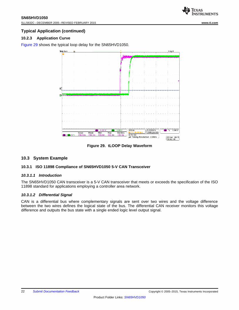
Transceiver loop delay is a measure of the overall device propagation delay, consisting of the delay from thedriver input (TXD pin) to the differential outputs (CANH and CANL pins), plus the delay from the receiver inputs(CANH and CANL) to its output (RXD pin). A typical loop delay for the SN65HVD1050 transceiver is displayed inFigure 29.
20 Submit Documentation Feedback Copyright © 2005–2015, Texas Instruments Incorporated
Product Folder Links: SN65HVD1050
SN65HVD1050
Transient
Clamp
Voltage
Transient
Current
SN65HVD1050www.ti.com SLLS632C –DECEMBER 2005–REVISED FEBRUARY 2015
Typical Application (continued)10.2.2 Detailed Design Procedure
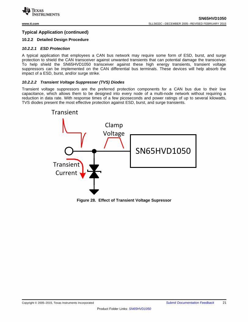
10.2.2.1 ESD ProtectionA typical application that employees a CAN bus network may require some form of ESD, burst, and surgeprotection to shield the CAN transceiver against unwanted transients that can potential damage the transceiver.To help shield the SN65HVD1050 transceiver against these high energy transients, transient voltagesuppressors can be implemented on the CAN differential bus terminals. These devices will help absorb theimpact of a ESD, burst, and/or surge strike.
10.2.2.2 Transient Voltage Suppresser (TVS) DiodesTransient voltage suppressors are the preferred protection components for a CAN bus due to their lowcapacitance, which allows them to be designed into every node of a multi-node network without requiring areduction in data rate. With response times of a few picoseconds and power ratings of up to several kilowatts,TVS diodes present the most effective protection against ESD, burst, and surge transients.
Figure 28. Effect of Transient Voltage Supressor
Copyright © 2005–2015, Texas Instruments Incorporated Submit Documentation Feedback 21
Product Folder Links: SN65HVD1050
SN65HVD1050SLLS632C –DECEMBER 2005–REVISED FEBRUARY 2015 www.ti.com
Typical Application (continued)10.2.3 Application CurveFigure 29 shows the typical loop delay for the SN65HVD1050.
Figure 29. tLOOP Delay Waveform
10.3 System Example
10.3.1 ISO 11898 Compliance of SN65HVD1050 5-V CAN Transceiver
10.3.1.1 IntroductionThe SN65HVD1050 CAN transceiver is a 5-V CAN transceiver that meets or exceeds the specification of the ISO11898 standard for applications employing a controller area network.
10.3.1.2 Differential SignalCAN is a differential bus where complementary signals are sent over two wires and the voltage differencebetween the two wires defines the logical state of the bus. The differential CAN receiver monitors this voltagedifference and outputs the bus state with a single ended logic level output signal.
22 Submit Documentation Feedback Copyright © 2005–2015, Texas Instruments Incorporated
Product Folder Links: SN65HVD1050
SN65HVD1050www.ti.com SLLS632C –DECEMBER 2005–REVISED FEBRUARY 2015
System Example (continued)
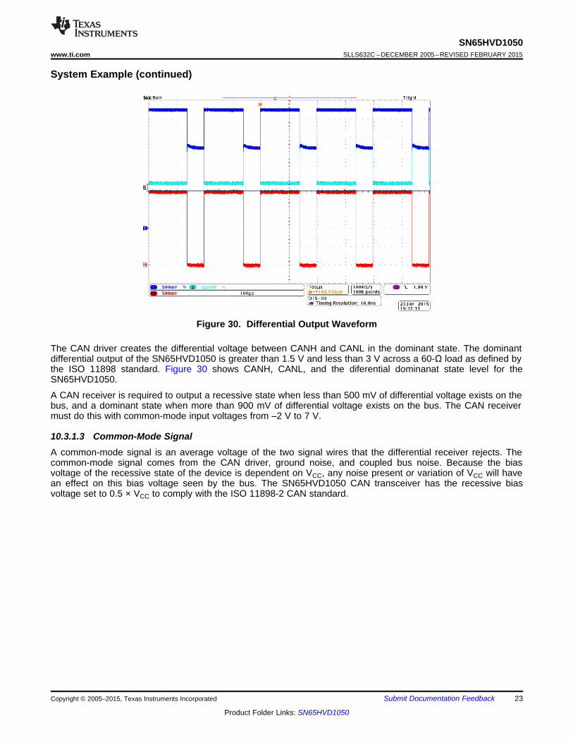
Figure 30. Differential Output Waveform
The CAN driver creates the differential voltage between CANH and CANL in the dominant state. The dominantdifferential output of the SN65HVD1050 is greater than 1.5 V and less than 3 V across a 60-Ω load as defined bythe ISO 11898 standard. Figure 30 shows CANH, CANL, and the diferential dominanat state level for theSN65HVD1050.
A CAN receiver is required to output a recessive state when less than 500 mV of differential voltage exists on thebus, and a dominant state when more than 900 mV of differential voltage exists on the bus. The CAN receivermust do this with common-mode input voltages from –2 V to 7 V.
10.3.1.3 Common-Mode SignalA common-mode signal is an average voltage of the two signal wires that the differential receiver rejects. Thecommon-mode signal comes from the CAN driver, ground noise, and coupled bus noise. Because the biasvoltage of the recessive state of the device is dependent on VCC, any noise present or variation of VCC will havean effect on this bias voltage seen by the bus. The SN65HVD1050 CAN transceiver has the recessive biasvoltage set to 0.5 × VCC to comply with the ISO 11898-2 CAN standard.
Copyright © 2005–2015, Texas Instruments Incorporated Submit Documentation Feedback 23
Product Folder Links: SN65HVD1050
SN65HVD1050SLLS632C –DECEMBER 2005–REVISED FEBRUARY 2015 www.ti.com
11 Power Supply RecommendationsTo ensure reliable operation at all data rates and supply voltages, each supply should be decoupled with a 100-nF ceramic capacitor located as close as possible to the VCC supply pins as possible. The SN65HVD1050 is alinear voltage regulator suitable for the 5-V supply rail.
12 Layout
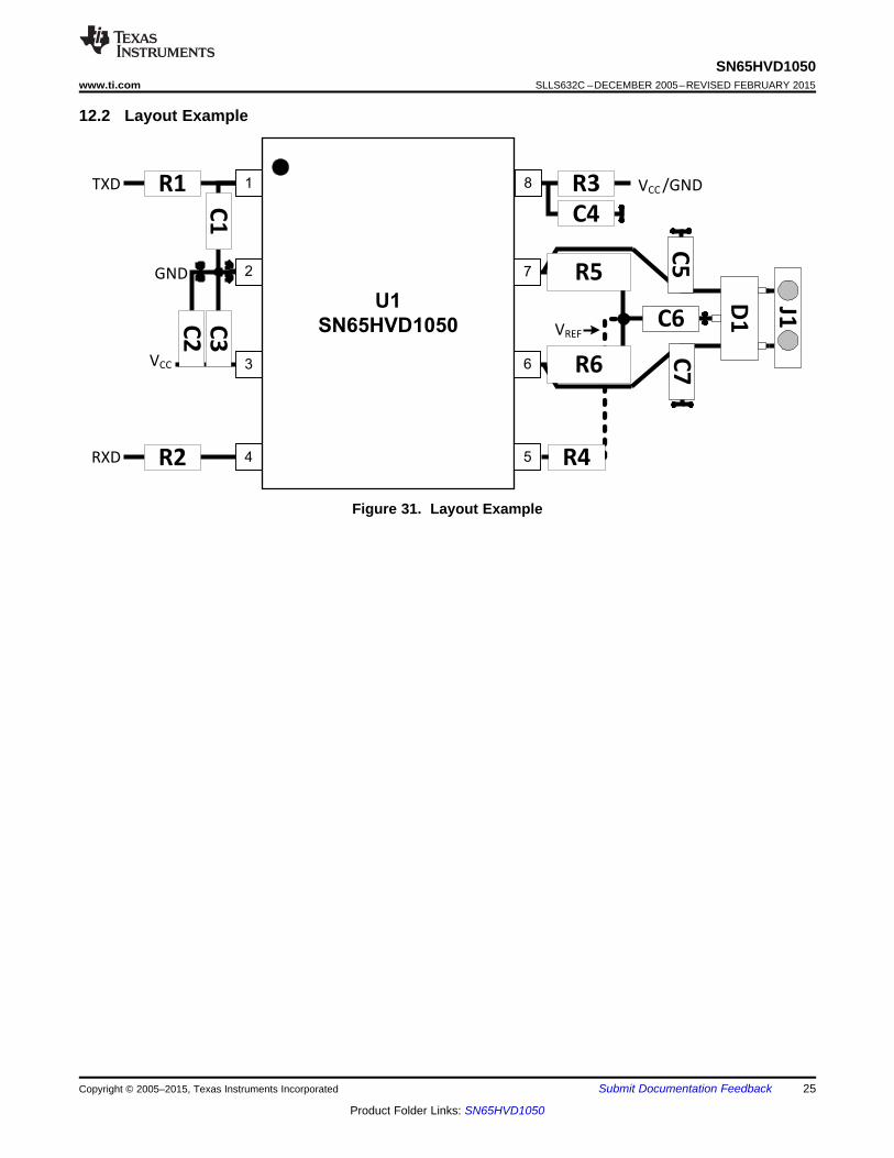
12.1 Layout GuidelinesIn order for the PCB design to be successful, start with design of the protection and filtering circuitry. BecauseESD and EFT transients have a wide frequency bandwidth from approximately 3-MHz to 3-GHz, high frequencylayout techniques must be applied during PCB design. On chip IEC ESD protection is good for laboratory andportable equipment but is usually not sufficient for EFT and surge transients occurring in industrial environments.Therefore robust and reliable bus node design requires the use of external transient protection devices at the busconnectors. Placement at the connector also prevents these harsh transient events from propagating further intothe PCB and system.
Use VCC and ground planes to provide low inductance.
NOTEHigh frequency current follows the path of least inductance and not the path of leastresistance.
Design the bus protection components in the direction of the signal path. Do not force the transient current todivert from the signal path to reach the protection device. An example placement of the Transient VoltageSuppression (TVS) device indicated as D1 (either bidirectional diode or varistor solution) and bus filter capacitorsC5 and C7 are shown in Figure 25.
The bus transient protection and filtering components should be placed as close to the bus connector, J1, aspossible. This prevents transients, ESD and noise from penetrating onto the board and disturbing other devices.
Bus termination: Figure 27 shows split termination. This is where the termination is split into two resistors, R5and R6, with the center or split tap of the termination connected to ground via capacitor C6. Split terminationprovides common mode filtering for the bus. When termination is placed on the board instead of directly on thebus, care must be taken to ensure the terminating node is not removed from the bus as this will cause signalintegrity issues of the bus is not properly terminated on both ends.
Bypass and bulk capacitors should be placed as close as possible to the supply pins of transceiver, examplesC2, C3 (VCC).
Use at least two vias for VCC and ground connections of bypass capacitors and protection devices to minimizetrace and via inductance.
To limit current of digital lines, serial resistors may be used. Examples are R1, R2, R3 and R4.
To filter noise on the digital IO lines, a capacitor may be used close to the input side of the IO as shown by C1and C4.
Because the internal pullup and pulldown biasing of the device is weak for floating pins, an external 1-kΩ to 10-kΩ pullup or pulldown resistor should be used to bias the state of the pin more strongly against noise duringtransient events.
Pin 1: If an open-drain host processor is used to drive the TXD pin of the device an external pullup resistorbetween 1 kΩ and 10 kΩ should be used to drive the recessive input state of the device.
Pin 5: VREF should be connected to the center point of a split temrination scheme to help stabalize the commonmode volatge to VCC/2. If VREF is unused it should be left floating.
Pin 8: Is shown assuming the mode pin, S, will be used. If the device will only be used in normal mode, R3 is notneeded and the pads of C4 could be used for the pulldown resistor to GND.
24 Submit Documentation Feedback Copyright © 2005–2015, Texas Instruments Incorporated
Product Folder Links: SN65HVD1050
1
2
3
4
U1
SN65HVD1050
8
7
6
5
R5
R6
C6
C5
D1
J1
VREF
C3
C2
VCC
GND
C1
R1
R2
R3 VCC /GND
C7
TXD
RXD R4
C4
SN65HVD1050www.ti.com SLLS632C –DECEMBER 2005–REVISED FEBRUARY 2015
12.2 Layout Example
Figure 31. Layout Example
Copyright © 2005–2015, Texas Instruments Incorporated Submit Documentation Feedback 25
Product Folder Links: SN65HVD1050
SN65HVD1050SLLS632C –DECEMBER 2005–REVISED FEBRUARY 2015 www.ti.com
13 Device and Documentation Support
13.1 TrademarksDeviceNet is a trademark of Open DeviceNet Vendors Association, Inc.All other trademarks are the property of their respective owners.
13.2 Electrostatic Discharge CautionThese devices have limited built-in ESD protection. The leads should be shorted together or the device placed in conductive foamduring storage or handling to prevent electrostatic damage to the MOS gates.
13.3 GlossarySLYZ022 — TI Glossary.
This glossary lists and explains terms, acronyms, and definitions.
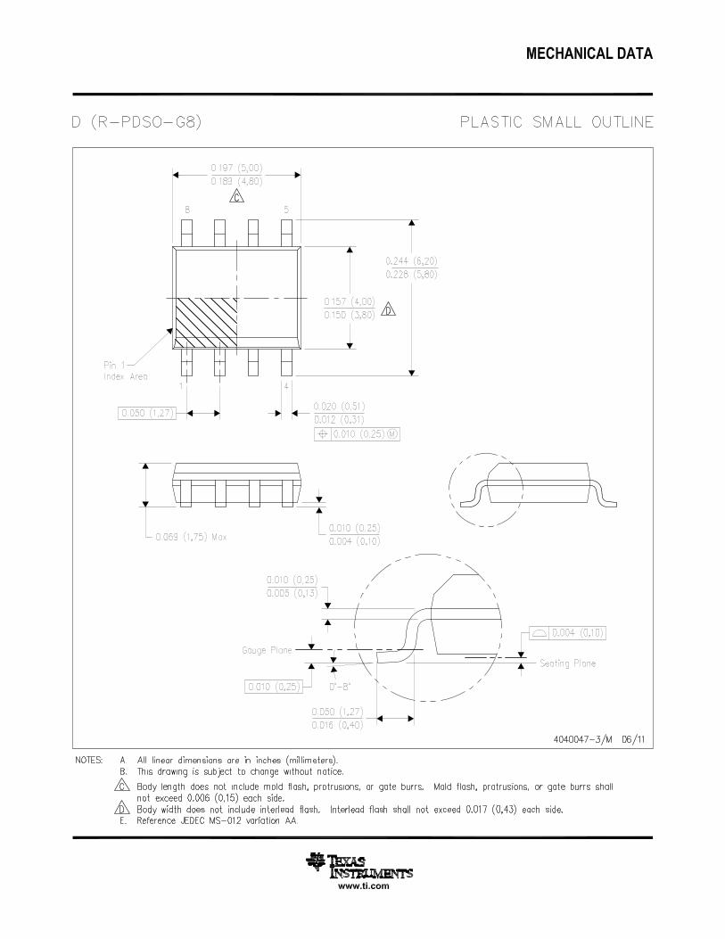
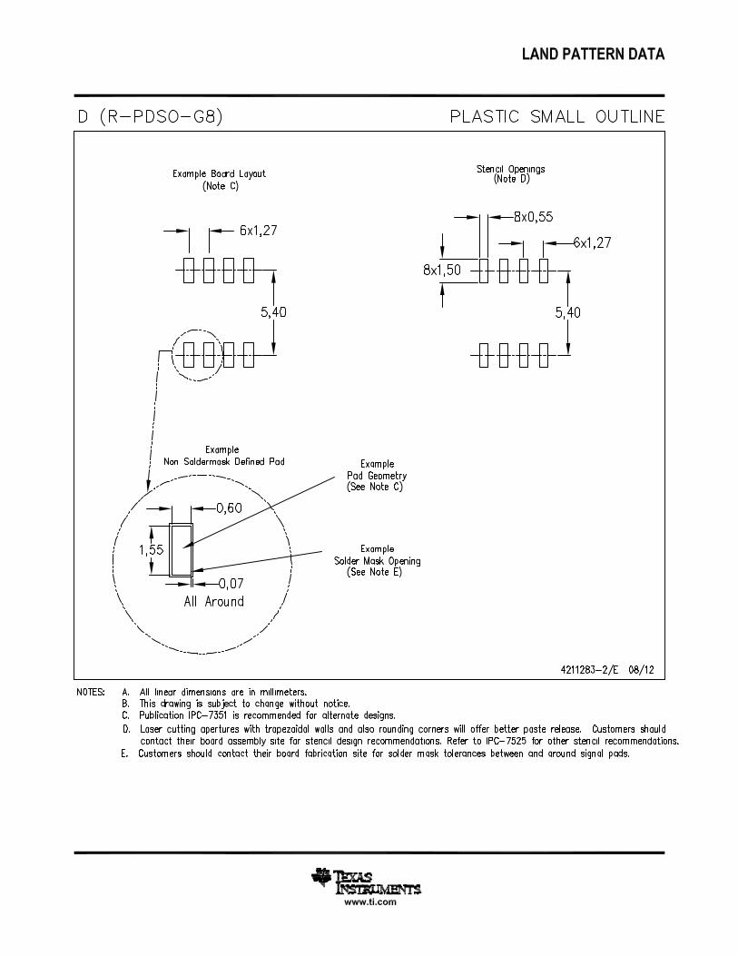
14 Mechanical, Packaging, and Orderable InformationThe following pages include mechanical, packaging, and orderable information. This information is the mostcurrent data available for the designated devices. This data is subject to change without notice and revision ofthis document. For browser-based versions of this data sheet, refer to the left-hand navigation.
26 Submit Documentation Feedback Copyright © 2005–2015, Texas Instruments Incorporated
Product Folder Links: SN65HVD1050
PACKAGE OPTION ADDENDUM
www.ti.com 7-May-2016
Addendum-Page 1
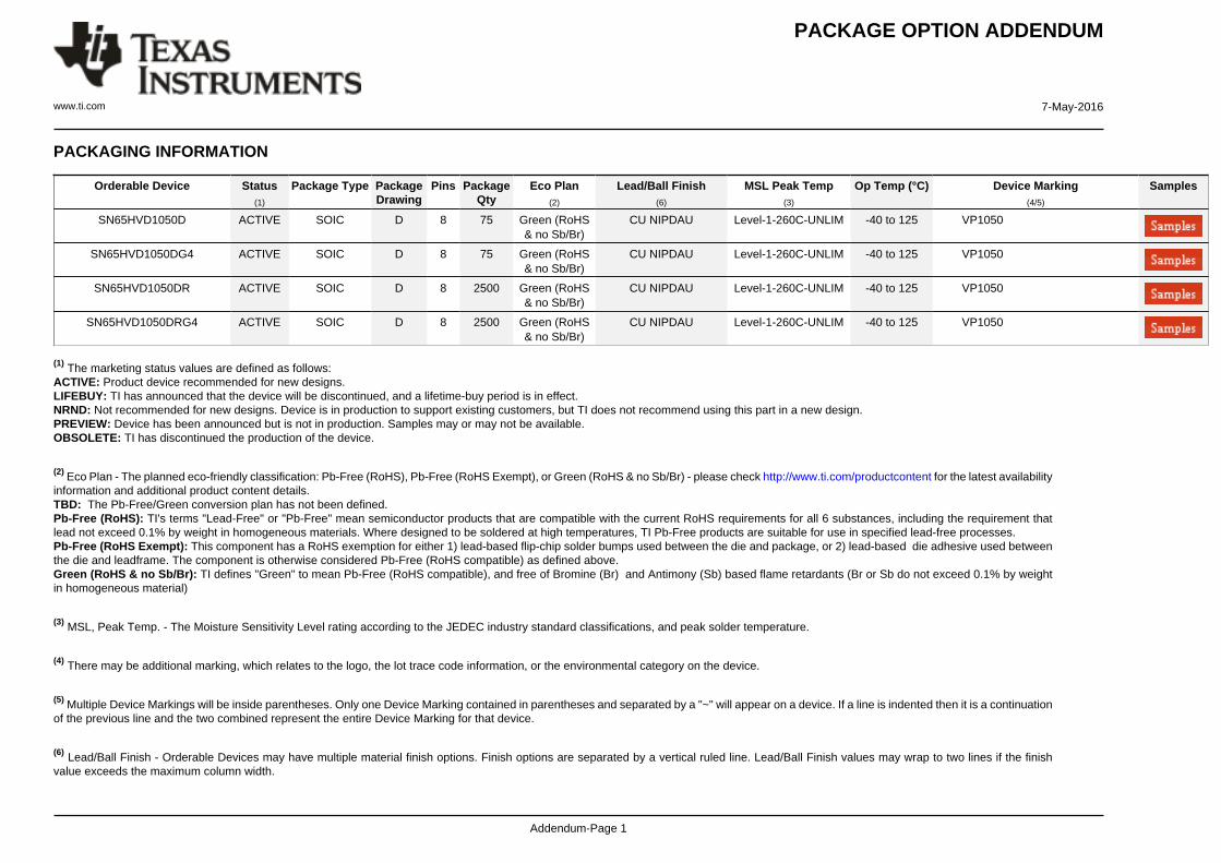
PACKAGING INFORMATION
Orderable Device Status(1)
Package Type PackageDrawing
Pins PackageQty
Eco Plan(2)
Lead/Ball Finish(6)
MSL Peak Temp(3)
Op Temp (°C) Device Marking(4/5)
Samples
SN65HVD1050D ACTIVE SOIC D 8 75 Green (RoHS& no Sb/Br)
CU NIPDAU Level-1-260C-UNLIM -40 to 125 VP1050
SN65HVD1050DG4 ACTIVE SOIC D 8 75 Green (RoHS& no Sb/Br)
CU NIPDAU Level-1-260C-UNLIM -40 to 125 VP1050
SN65HVD1050DR ACTIVE SOIC D 8 2500 Green (RoHS& no Sb/Br)
CU NIPDAU Level-1-260C-UNLIM -40 to 125 VP1050
SN65HVD1050DRG4 ACTIVE SOIC D 8 2500 Green (RoHS& no Sb/Br)
CU NIPDAU Level-1-260C-UNLIM -40 to 125 VP1050
(1) The marketing status values are defined as follows:ACTIVE: Product device recommended for new designs.LIFEBUY: TI has announced that the device will be discontinued, and a lifetime-buy period is in effect.NRND: Not recommended for new designs. Device is in production to support existing customers, but TI does not recommend using this part in a new design.PREVIEW: Device has been announced but is not in production. Samples may or may not be available.OBSOLETE: TI has discontinued the production of the device.
(2) Eco Plan - The planned eco-friendly classification: Pb-Free (RoHS), Pb-Free (RoHS Exempt), or Green (RoHS & no Sb/Br) - please check http://www.ti.com/productcontent for the latest availabilityinformation and additional product content details.TBD: The Pb-Free/Green conversion plan has not been defined.Pb-Free (RoHS): TI's terms "Lead-Free" or "Pb-Free" mean semiconductor products that are compatible with the current RoHS requirements for all 6 substances, including the requirement thatlead not exceed 0.1% by weight in homogeneous materials. Where designed to be soldered at high temperatures, TI Pb-Free products are suitable for use in specified lead-free processes.Pb-Free (RoHS Exempt): This component has a RoHS exemption for either 1) lead-based flip-chip solder bumps used between the die and package, or 2) lead-based die adhesive used betweenthe die and leadframe. The component is otherwise considered Pb-Free (RoHS compatible) as defined above.Green (RoHS & no Sb/Br): TI defines "Green" to mean Pb-Free (RoHS compatible), and free of Bromine (Br) and Antimony (Sb) based flame retardants (Br or Sb do not exceed 0.1% by weightin homogeneous material)
(3) MSL, Peak Temp. - The Moisture Sensitivity Level rating according to the JEDEC industry standard classifications, and peak solder temperature.
(4) There may be additional marking, which relates to the logo, the lot trace code information, or the environmental category on the device.
(5) Multiple Device Markings will be inside parentheses. Only one Device Marking contained in parentheses and separated by a "~" will appear on a device. If a line is indented then it is a continuationof the previous line and the two combined represent the entire Device Marking for that device.
(6) Lead/Ball Finish - Orderable Devices may have multiple material finish options. Finish options are separated by a vertical ruled line. Lead/Ball Finish values may wrap to two lines if the finishvalue exceeds the maximum column width.
PACKAGE OPTION ADDENDUM
www.ti.com 7-May-2016
Addendum-Page 2
Important Information and Disclaimer:The information provided on this page represents TI's knowledge and belief as of the date that it is provided. TI bases its knowledge and belief on informationprovided by third parties, and makes no representation or warranty as to the accuracy of such information. Efforts are underway to better integrate information from third parties. TI has taken andcontinues to take reasonable steps to provide representative and accurate information but may not have conducted destructive testing or chemical analysis on incoming materials and chemicals.TI and TI suppliers consider certain information to be proprietary, and thus CAS numbers and other limited information may not be available for release.
In no event shall TI's liability arising out of such information exceed the total purchase price of the TI part(s) at issue in this document sold by TI to Customer on an annual basis.
OTHER QUALIFIED VERSIONS OF SN65HVD1050 :
• Automotive: SN65HVD1050-Q1
• Enhanced Product: SN65HVD1050-EP
NOTE: Qualified Version Definitions:
• Automotive - Q100 devices qualified for high-reliability automotive applications targeting zero defects
• Enhanced Product - Supports Defense, Aerospace and Medical Applications
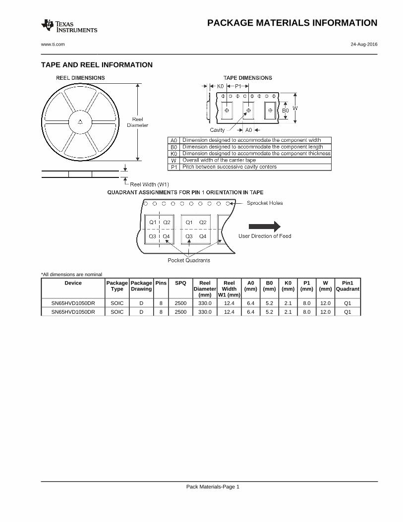
TAPE AND REEL INFORMATION
*All dimensions are nominal
Device PackageType
PackageDrawing
Pins SPQ ReelDiameter
(mm)
ReelWidth
W1 (mm)
A0(mm)
B0(mm)
K0(mm)
P1(mm)
W(mm)
Pin1Quadrant
SN65HVD1050DR SOIC D 8 2500 330.0 12.4 6.4 5.2 2.1 8.0 12.0 Q1
SN65HVD1050DR SOIC D 8 2500 330.0 12.4 6.4 5.2 2.1 8.0 12.0 Q1
PACKAGE MATERIALS INFORMATION
www.ti.com 24-Aug-2016
Pack Materials-Page 1
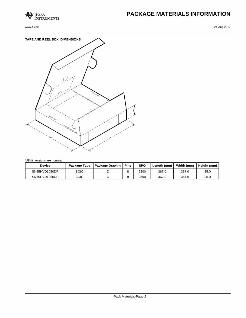
*All dimensions are nominal
Device Package Type Package Drawing Pins SPQ Length (mm) Width (mm) Height (mm)
SN65HVD1050DR SOIC D 8 2500 367.0 367.0 35.0
SN65HVD1050DR SOIC D 8 2500 367.0 367.0 38.0
PACKAGE MATERIALS INFORMATION
www.ti.com 24-Aug-2016
Pack Materials-Page 2
IMPORTANT NOTICE
Texas Instruments Incorporated and its subsidiaries (TI) reserve the right to make corrections, enhancements, improvements and otherchanges to its semiconductor products and services per JESD46, latest issue, and to discontinue any product or service per JESD48, latestissue. Buyers should obtain the latest relevant information before placing orders and should verify that such information is current andcomplete. All semiconductor products (also referred to herein as “components”) are sold subject to TI’s terms and conditions of salesupplied at the time of order acknowledgment.TI warrants performance of its components to the specifications applicable at the time of sale, in accordance with the warranty in TI’s termsand conditions of sale of semiconductor products. Testing and other quality control techniques are used to the extent TI deems necessaryto support this warranty. Except where mandated by applicable law, testing of all parameters of each component is not necessarilyperformed.TI assumes no liability for applications assistance or the design of Buyers’ products. Buyers are responsible for their products andapplications using TI components. To minimize the risks associated with Buyers’ products and applications, Buyers should provideadequate design and operating safeguards.TI does not warrant or represent that any license, either express or implied, is granted under any patent right, copyright, mask work right, orother intellectual property right relating to any combination, machine, or process in which TI components or services are used. Informationpublished by TI regarding third-party products or services does not constitute a license to use such products or services or a warranty orendorsement thereof. Use of such information may require a license from a third party under the patents or other intellectual property of thethird party, or a license from TI under the patents or other intellectual property of TI.Reproduction of significant portions of TI information in TI data books or data sheets is permissible only if reproduction is without alterationand is accompanied by all associated warranties, conditions, limitations, and notices. TI is not responsible or liable for such altereddocumentation. Information of third parties may be subject to additional restrictions.Resale of TI components or services with statements different from or beyond the parameters stated by TI for that component or servicevoids all express and any implied warranties for the associated TI component or service and is an unfair and deceptive business practice.TI is not responsible or liable for any such statements.Buyer acknowledges and agrees that it is solely responsible for compliance with all legal, regulatory and safety-related requirementsconcerning its products, and any use of TI components in its applications, notwithstanding any applications-related information or supportthat may be provided by TI. Buyer represents and agrees that it has all the necessary expertise to create and implement safeguards whichanticipate dangerous consequences of failures, monitor failures and their consequences, lessen the likelihood of failures that might causeharm and take appropriate remedial actions. Buyer will fully indemnify TI and its representatives against any damages arising out of the useof any TI components in safety-critical applications.In some cases, TI components may be promoted specifically to facilitate safety-related applications. With such components, TI’s goal is tohelp enable customers to design and create their own end-product solutions that meet applicable functional safety standards andrequirements. Nonetheless, such components are subject to these terms.No TI components are authorized for use in FDA Class III (or similar life-critical medical equipment) unless authorized officers of the partieshave executed a special agreement specifically governing such use.Only those TI components which TI has specifically designated as military grade or “enhanced plastic” are designed and intended for use inmilitary/aerospace applications or environments. Buyer acknowledges and agrees that any military or aerospace use of TI componentswhich have not been so designated is solely at the Buyer's risk, and that Buyer is solely responsible for compliance with all legal andregulatory requirements in connection with such use.TI has specifically designated certain components as meeting ISO/TS16949 requirements, mainly for automotive use. In any case of use ofnon-designated products, TI will not be responsible for any failure to meet ISO/TS16949.
Products ApplicationsAudio www.ti.com/audio Automotive and Transportation www.ti.com/automotiveAmplifiers amplifier.ti.com Communications and Telecom www.ti.com/communicationsData Converters dataconverter.ti.com Computers and Peripherals www.ti.com/computersDLP® Products www.dlp.com Consumer Electronics www.ti.com/consumer-appsDSP dsp.ti.com Energy and Lighting www.ti.com/energyClocks and Timers www.ti.com/clocks Industrial www.ti.com/industrialInterface interface.ti.com Medical www.ti.com/medicalLogic logic.ti.com Security www.ti.com/securityPower Mgmt power.ti.com Space, Avionics and Defense www.ti.com/space-avionics-defenseMicrocontrollers microcontroller.ti.com Video and Imaging www.ti.com/videoRFID www.ti-rfid.comOMAP Applications Processors www.ti.com/omap TI E2E Community e2e.ti.comWireless Connectivity www.ti.com/wirelessconnectivity
Mailing Address: Texas Instruments, Post Office Box 655303, Dallas, Texas 75265Copyright © 2016, Texas Instruments Incorporated