SLES244B – FEBRUARY 2009– REVISED MARCH 2013 … · Burr-Brown Audio PCM5310 PCM5310 SLES244B...
104
Burr-Brown Audio PCM5310 PCM5310 www.ti.com SLES244B – FEBRUARY 2009 – REVISED MARCH 2013 24-Bit, 96-/192-kHz, Asynchronous, 4-Channel/4-Channel Audio Codec with 2-V RMS Driver, Headphone Driver, and 6 Audio Interface Ports Check for Samples: PCM5310 1FEATURES • Power-Supply Voltage: – 9 V for 2-V RMS Driver 234• 2- or 2.4-V RMS Output (Typ), 2-V RMS Input (Typ) – 3.3 V for Digital and Analog • Asynchronous Operation for 2 Stereo DACs and 2 Stereo ADCs • Power Consumption: • 6 Audio Interface Ports with Mux and Bypass – 360 mW at f S = 48-kHz Operation • Performance: – 25.5 μW in Power-Down Mode – THD+N (f S = 48 kHz): • Pop Noise Reduction at Clock Halt 0.01% (ADC), 0.01% (DAC) • Short-Circuit Protection for Headphone Output – SNR/DR (f S = 48 kHz): • Flexible GPIO Port: 95 dB (ADC), 100 dB (DAC) – Internal Mute Flag – Line Input (Stereo x6): – Internal Zero Flag Available for 2-V RMS Input – Headphone Insertion Detection Status – Line Output (Stereo x2): – Headphone Short-Circuit Protection Status Available for 2-V RMS or 2.4-V RMS Output – Logic Functions (AND, NAND, OR, NOR, – Headphone Output: BUF, INV) > 20 mW into 32 Ω, > 30 mW into 16 Ω • Package: 64-Pin HTQFP PowerPAD™ – Sampling Rate: • Operating Temperature Range:–25°C to +85°C 96 kHz (ADC), 192 kHz (DAC) – System Clock: APPLICATIONS 128 f S , 192 f S , 256 f S , 384 f S , 512 f S , 768 f S • Digital TV – Digital Filter Passband Ripple: ±0.05 dB (ADC), ±0.04 dB (DAC) • DVD Recorder – Digital Filter Stop Band Attenuation: • IP-STB (Set Top Box) –65 dB (ADC), –50 dB (DAC) DESCRIPTION • I 2 C™ Interface The PCM5310 is a four-channel/four-channel audio • Multifunctions: codec with a 2-V RMS driver, headphone amplifier, – Audio Interface: analog multiplexer (mux), and six audio interface I 2 S™, Left-Justified, and Right-Justified ports for digital TV applications. – Digital Attenuation: The PCM5310 accepts left-justified, right-justified, 0 dB to –100 dB in 0.5-dB Steps (DAC), and I 2 S audio data formats with 16 or 24 bits. The 20 dB to –100 dB in 0.5-dB Steps (ADC) PCM5310 also incorporates many functions through – Digital Soft Mute: 1.0-dB Steps to Mute the I 2 C interface, such as an analog bypass mode, analog volume control, analog level control, analog – Digital De-Emphasis Filter: 32, 44.1, 48 kHz multiplexer, GPIO, zero flag, short protection, de- – Digital Audio Interface Mux and Bypass emphasis filter, high-pass filter, and digital attenuator. – Line Input Level Control: 9, 6, 3, 0 dB The six audio interface ports each have a built-in digital mux and bypass functions to reduce the need – Line Output Level Control: 0, –0.5, –1.0 dB for additional DSP ports or other devices. – Headphone Output Volume Control: 12 dB to –70 dB in 1-dB Steps – Oversampling Rate Control for DAC 1 Please be aware that an important notice concerning availability, standard warranty, and use in critical applications of Texas Instruments semiconductor products and disclaimers thereto appears at the end of this data sheet. 2PowerPAD is a trademark of Texas Instruments. 3I 2 C, I 2 S are trademarks of NXP Semiconductors. 4All other trademarks are the property of their respective owners. PRODUCTION DATA information is current as of publication date. Copyright © 2009–2013, Texas Instruments Incorporated Products conform to specifications per the terms of the Texas Instruments standard warranty. Production processing does not necessarily include testing of all parameters.
Transcript of SLES244B – FEBRUARY 2009– REVISED MARCH 2013 … · Burr-Brown Audio PCM5310 PCM5310 SLES244B...

Burr-Brown Audio
PCM5310PCM5310
www.ti.com SLES244B –FEBRUARY 2009–REVISED MARCH 2013
24-Bit, 96-/192-kHz, Asynchronous, 4-Channel/4-Channel Audio Codecwith 2-VRMS Driver, Headphone Driver, and 6 Audio Interface Ports
Check for Samples: PCM5310
1FEATURES • Power-Supply Voltage:– 9 V for 2-VRMS Driver
234• 2- or 2.4-VRMS Output (Typ), 2-VRMS Input (Typ)– 3.3 V for Digital and Analog• Asynchronous Operation for 2 Stereo DACs
and 2 Stereo ADCs • Power Consumption:• 6 Audio Interface Ports with Mux and Bypass – 360 mW at fS = 48-kHz Operation• Performance: – 25.5 μW in Power-Down Mode
– THD+N (fS = 48 kHz): • Pop Noise Reduction at Clock Halt0.01% (ADC), 0.01% (DAC) • Short-Circuit Protection for Headphone Output
– SNR/DR (fS = 48 kHz): • Flexible GPIO Port:95 dB (ADC), 100 dB (DAC) – Internal Mute Flag
– Line Input (Stereo x6): – Internal Zero FlagAvailable for 2-VRMS Input
– Headphone Insertion Detection Status– Line Output (Stereo x2):
– Headphone Short-Circuit Protection StatusAvailable for 2-VRMS or 2.4-VRMS Output– Logic Functions (AND, NAND, OR, NOR,– Headphone Output:
BUF, INV)> 20 mW into 32 Ω, > 30 mW into 16 Ω• Package: 64-Pin HTQFP PowerPAD™– Sampling Rate:• Operating Temperature Range:–25°C to +85°C96 kHz (ADC), 192 kHz (DAC)
– System Clock:APPLICATIONS128 fS, 192 fS, 256 fS, 384 fS, 512 fS, 768 fS• Digital TV– Digital Filter Passband Ripple:
±0.05 dB (ADC), ±0.04 dB (DAC) • DVD Recorder– Digital Filter Stop Band Attenuation: • IP-STB (Set Top Box)
–65 dB (ADC), –50 dB (DAC)DESCRIPTION• I2C™ InterfaceThe PCM5310 is a four-channel/four-channel audio• Multifunctions:codec with a 2-VRMS driver, headphone amplifier,
– Audio Interface: analog multiplexer (mux), and six audio interfaceI2S™, Left-Justified, and Right-Justified ports for digital TV applications.
– Digital Attenuation:The PCM5310 accepts left-justified, right-justified,
0 dB to –100 dB in 0.5-dB Steps (DAC), and I2S audio data formats with 16 or 24 bits. The20 dB to –100 dB in 0.5-dB Steps (ADC) PCM5310 also incorporates many functions through
– Digital Soft Mute: 1.0-dB Steps to Mute the I2C interface, such as an analog bypass mode,analog volume control, analog level control, analog– Digital De-Emphasis Filter: 32, 44.1, 48 kHzmultiplexer, GPIO, zero flag, short protection, de-
– Digital Audio Interface Mux and Bypass emphasis filter, high-pass filter, and digital attenuator.– Line Input Level Control: 9, 6, 3, 0 dB The six audio interface ports each have a built-in
digital mux and bypass functions to reduce the need– Line Output Level Control: 0, –0.5, –1.0 dBfor additional DSP ports or other devices.– Headphone Output Volume Control:
12 dB to –70 dB in 1-dB Steps– Oversampling Rate Control for DAC
1
Please be aware that an important notice concerning availability, standard warranty, and use in critical applications ofTexas Instruments semiconductor products and disclaimers thereto appears at the end of this data sheet.
2PowerPAD is a trademark of Texas Instruments.3I2C, I2S are trademarks of NXP Semiconductors.4All other trademarks are the property of their respective owners.
PRODUCTION DATA information is current as of publication date. Copyright © 2009–2013, Texas Instruments IncorporatedProducts conform to specifications per the terms of the TexasInstruments standard warranty. Production processing does notnecessarily include testing of all parameters.

PCM5310
SLES244B –FEBRUARY 2009–REVISED MARCH 2013 www.ti.com
This integrated circuit can be damaged by ESD. Texas Instruments recommends that all integrated circuits be handled withappropriate precautions. Failure to observe proper handling and installation procedures can cause damage.
ESD damage can range from subtle performance degradation to complete device failure. Precision integrated circuits may be moresusceptible to damage because very small parametric changes could cause the device not to meet its published specifications.
PACKAGING/ORDERING INFORMATION
For the most current package and ordering information, see the Package Option Addendum at the end of thisdocument, or see the TI website at www.ti.com.
ABSOLUTE MAXIMUM RATINGS (1)
Over operating free-air temperature range (unless otherwise noted).
PCM5310 UNIT
VCCDA, VCCAD, VCCP, VDD –0.3 to 4.0 VSupply voltage
VCCH –0.3 to 10 V
Ground voltage differences: AGNDAD, AGNDDA, PGND, HGND, DGND ±0.1 V
Input voltage –0.3 to 4.0 V
Input current (all pins except supplies) ±10 mA
Ambient temperature under bias –40 to +125 °C
Storage temperature –55 to +150 °C
Junction temperature +150 °C
Lead temperature (soldering, 5s) +260 °C
Package temperature (IR reflow, peak) +260 °C
(1) Stresses beyond those listed under Absolute Maximum Ratings may cause permanent damage to the device. These are stress ratingsonly, and functional operation of the device at these or any other conditions beyond those indicated under Recommended OperatingConditions is not implied. Exposure to absolute-maximum-rated conditions for extended periods may affect device reliability.
RECOMMENDED OPERATING CONDITIONSOver operating free-air temperature range (unless otherwise noted).
PARAMETER MIN NOM MAX UNIT
Analog supply voltage, VCCAD, VCCDA, VCCP 3.0 3.3 3.6 V
Analog supply voltage, VCCH 8.55 9 9.45 V
Digital supply voltage, VDD 3.0 3.3 3.6 V
Analog input voltage, full-scale (–0 dB) 2 VRMS
Analog output voltage, full-scale (–0 dB) 2 2.4 VRMS
Digital input logic family CMOS
ADC system clock 4.096 36.864 MHz
ADC sampling clock 32 96 kHzDigital input clock frequency
DAC system clock 4.096 36.864 MHz
DAC sampling clock 32 192 kHz
Analog output load resistance 10 kΩAnalog output load capacitance 30 pF
Digital output load capacitance 10 pF
Operating free-air temperature, TA –25 +85 °C
2 Submit Documentation Feedback Copyright © 2009–2013, Texas Instruments Incorporated
Product Folder Links: PCM5310

PCM5310
www.ti.com SLES244B –FEBRUARY 2009–REVISED MARCH 2013
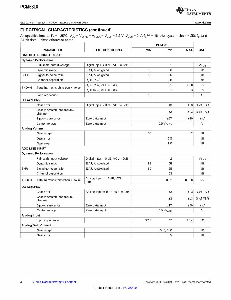
ELECTRICAL CHARACTERISTICSAll specifications at TA = +25°C, VDD = VCCAD = VCCDA = VCCP = 3.3 V, VCCH = 9 V, fS
(1) = 48 kHz, system clock = 256 fS, and24-bit data, unless otherwise noted.
PCM5310
PARAMETER TEST CONDITIONS MIN TYP MAX UNIT
AUDIO DATA
Data Format
Audio data bit length 16, 24 Bits
Audio data interface format I2S, left-justified, right-justified
Audio data format MSB, twos complement
ADC 108 kHzSamplingfrequency DAC 216 kHz
ADC 256 fS, 384 fS, 512 fS, 768 fS MHzSystem clock
DAC 128 fS, 192 fS, 256 fS, 384 fS, 512 fS, 768 fS MHz
ADC 48 fS, 64 fS MHzBit clock
DAC 32 fS, 48 fS, 64 fS MHz
DIGITAL INPUT/OUTPUT
Logic family CMOS-compatible
VIH Input logic high level 0.7 VDD V
VIL Input logic low level 0.3 VDD V
IIH Input logic high current 10 μA
IIL Input logic low current –10 μA
VOH Output logic high level IOH = 2 mA 0.75 VDD V
VOL Output logic low level IOH = –2 mA 0.25 VDD V
DAC LINE OUTPUT
Dynamic Performance
Digital input = 0 dB, G242, G241 2 VRMS= lowFull-scale output voltage
Digital input = 0 dB, G242, G241 2.4 VRMS= high
Dynamic range EIAJ, A-weighted 90 100 dB
SNR Signal-to-noise ratio EIAJ, A-weighted 90 100 dB
Channel separation 88 97 dB
Digital input = 0 dB, G242, G241THD+N Total harmonic distortion + noise 0.01 0.02 %= low
Load resistance AC load 10 kΩDC Accuracy
Digital input = 0 dB, G242, G241Gain error ±3 ±13 % of FSR= low
Gain mismatch, channel-to- ±3 ±13 % of FSRchannel
Bipolar zero error Zero data input ±40 ±120 mV
Center voltage Zero data input 0.5 VCCDA V
Analog Gain Control
Gain range 0, –0.5, –1.0 dB
Gain error ±0.5 dB
(1) fS = sampling rate.
Copyright © 2009–2013, Texas Instruments Incorporated Submit Documentation Feedback 3
Product Folder Links: PCM5310
PCM5310
SLES244B –FEBRUARY 2009–REVISED MARCH 2013 www.ti.com
ELECTRICAL CHARACTERISTICS (continued)All specifications at TA = +25°C, VDD = VCCAD = VCCDA = VCCP = 3.3 V, VCCH = 9 V, fS
(1) = 48 kHz, system clock = 256 fS, and24-bit data, unless otherwise noted.
PCM5310
PARAMETER TEST CONDITIONS MIN TYP MAX UNIT
DAC HEADPHONE OUTPUT
Dynamic Performance
Full-scale output voltage Digital input = 0 dB, VOL = 0dB 1 VRMS
Dynamic range EIAJ, A-weighted 85 96 dB
SNR Signal-to-noise ratio EIAJ, A-weighted 85 96 dB
Channel separation RL = 32 Ω 88 dB
RL = 32 Ω, VOL = 0 dB 0.1 0.18 %THD+N Total harmonic distortion + noise
RL = 16 Ω, VOL = 0 dB 1 3 %
Load resistance 16 ΩDC Accuracy
Gain error Digital input = 0 dB, VOL = 0dB ±3 ±13 % of FSR
Gain mismatch, channel-to- ±3 ±13 % of FSRchannel
Bipolar zero error Zero data input ±27 ±80 mV
Center voltage Zero data input 0.5 VCCDA V
Analog Volume
Gain range –70 12 dB
Gain error 0.5 dB
Gain step 1.0 dB
ADC LINE INPUT
Dynamic Performance
Full-scale input voltage Digital input = 0 dB, VOL = 0dB 2 VRMS
Dynamic range EIAJ, A-weighted 85 95 dB
SNR Signal-to-noise ratio EIAJ, A-weighted 85 95 dB
Channel separation 93 dB
Analog input = –1 dB, VOL =THD+N Total harmonic distortion + noise 0.01 0.018 %0dB
DC Accuracy
Gain error Analog input = 0 dB, VOL = 0dB ±3 ±13 % of FSR
Gain mismatch, channel-to- ±3 ±13 % of FSRchannel
Bipolar zero error Zero data input ±17 ±50 mV
Center voltage Zero data input 0.5 VCCAD V
Analog Input
Input impedance 37.6 47 56.4 kΩAnalog Gain Control
Gain range 9, 6, 3, 0 dB
Gain error ±0.5 dB
4 Submit Documentation Feedback Copyright © 2009–2013, Texas Instruments Incorporated
Product Folder Links: PCM5310

PCM5310
www.ti.com SLES244B –FEBRUARY 2009–REVISED MARCH 2013
ELECTRICAL CHARACTERISTICS (continued)All specifications at TA = +25°C, VDD = VCCAD = VCCDA = VCCP = 3.3 V, VCCH = 9 V, fS
(1) = 48 kHz, system clock = 256 fS, and24-bit data, unless otherwise noted.
PCM5310
PARAMETER TEST CONDITIONS MIN TYP MAX UNIT
ANALOG INPUT TO ANALOG OUTPUT PATH (BYPASS)
Dynamic Performance
Full-scale input voltage Analog input = 0 dB, VOL = 0dB 2 VRMS
Analog input = 0 dB, G242,Full-scale output voltage 2 VRMSG241 = low
Dynamic range EIAJ, A-weighted 90 100 dB
SNR Signal-to-noise ratio EIAJ, A-weighted 90 100 dB
Channel separation 88 97 dB
Analog input = 0 dB, G242,THD+N Total harmonic distortion + noise 0.003 0.006 %G241 = low
DC Accuracy
Analog input = 0 dB, G242,Gain error ±3 ±13 % of FSRG241 = low
Gain mismatch, channel-to- 3 ±13 % of FSRchannel
Bipolar zero error Zero data input ±20 ±60 mV
analog input Zero data input 0.5 VCCAD VCenter voltage
analog output Zero data input 0.5 VCCDA V
Analog Input
Input impedance 37.6 47 56.4 kΩFILTERS
Interpolation Filters for DAC
Passband 0.454 f S kHz
Stop band 0.546 f S kHz
Passband ripple ±0.04 dB
Stop-band attenuation –50 dB
Group delay 20/fS s
De-emphasis error ±0.1 dB
Analog Filter for DAC
Frequency response fC = 20 kHz ±0.1 dB
Cutoff frequency Gain = –3 dB 190 kHz
Decimation Filter for ADC
Passband 0.454 f S kHz
Stop band 0.583 f S kHz
Passband ripple ±0.05 dB
Stop-band attenuation –65 dB
Group delay 17.4/fS s
Analog Filter for ADC
Frequency response fC = 20 kHz ±0.01 dB
Cutoff frequency Gain = –3 dB 500 kHz
High-Pass Filter for ADC
Frequency response Gain = –3 dB 0.91 Hz
Copyright © 2009–2013, Texas Instruments Incorporated Submit Documentation Feedback 5
Product Folder Links: PCM5310

PCM5310
SLES244B –FEBRUARY 2009–REVISED MARCH 2013 www.ti.com
ELECTRICAL CHARACTERISTICS (continued)All specifications at TA = +25°C, VDD = VCCAD = VCCDA = VCCP = 3.3 V, VCCH = 9 V, fS
(1) = 48 kHz, system clock = 256 fS, and24-bit data, unless otherwise noted.
PCM5310
PARAMETER TEST CONDITIONS MIN TYP MAX UNIT
POWER-SUPPLY REQUIREMENTS
VDD Digital voltage range 3 3.3 3.6 V
VCCAD DAC voltage range 3 3.3 3.6 V
VCCDA ADC voltage range 3 3.3 3.6 V
VCCP Headphone driver voltage range 3 3.3 3.6 V
VCCH 2-VRMS driver voltage range 8.55 9 9.45 V
Zero data input, all active 98 120 mASupply current
All power-down 6 100 μA
Zaro data input, all active 360 450 mWPower dissipation
All power-down 25.5 350 μW
TEMPERATURE RANGE
Operating temperature range –25 +85 °C
θJA Thermal resistance HTQFP-64 21 °C/W
6 Submit Documentation Feedback Copyright © 2009–2013, Texas Instruments Incorporated
Product Folder Links: PCM5310
48
47
46
45
44
43
42
41
40
39
38
37
36
35
34
33
BCK5
SCK5
DATA4
LRCK4
BCK4
SCK4
DGND
VDD
DATA3
LRCK3
BCK3
SCK3
DATA2
LRCK2
BCK2
SCK2
1
2
3
4
5
6
7
8
9
10
11
12
13
14
15
16
AIN1L
AIN1R
AIN2L
AIN2R
AIN3L
AIN3R
AIN4L
AIN4R
AIN5L
AIN5R
AIN6L
AIN6R
LO1L
LO1R
LO2L
LO2R
VC
OM
AD
HG
ND
VR
EF
AD
2V
CC
H
VR
EF
AD
1H
PO
L
AG
ND
AD
VC
CP
VC
CA
DP
GN
D
AM
UT
EH
PO
R
RS
TB
VC
CD
A
GP
IO3
AG
ND
DA
GP
IO2
VC
OM
DA
GP
IO1
AG
ND
S
DA
TA
6S
DA
LR
CK
6S
CL
BC
K6
SC
K1
SC
K6
BC
K1
DA
TA
5LR
CK
1
LR
CK
5D
ATA
1
64 63 62 61 60 59 58 57 56 55 54
17 18 19 20 21 22 23 24 25 26 27
53 52 51 50 49
28 29 30 31 32
PCM5310
PowerPAD
PCM5310
www.ti.com SLES244B –FEBRUARY 2009–REVISED MARCH 2013
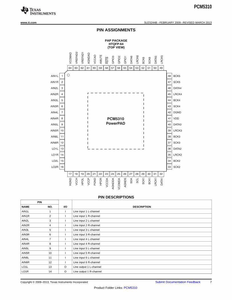
PIN ASSIGNMENTS
PAP PACKAGEHTQFP-64
(TOP VIEW)
PIN DESCRIPTIONSPIN
NAME NO. I/O DESCRIPTION
AIN1L 1 I Line input 1 L-channel
AIN1R 2 I Line input 1 R-channel
AIN2L 3 I Line input 2 L-channel
AIN2R 4 I Line input 2 R-channel
AIN3L 5 I Line input 3 L-channel
AIN3R 6 I Line input 3 R-channel
AIN4L 7 I Line input 4 L-channel
AIN4R 8 I Line input 4 R-channel
AIN5L 9 I Line input 5 L-channel
AIN5R 10 I Line input 5 R-channel
AIN6L 11 I Line input 6 L-channel
AIN6R 12 I Line input 6 R-channel
LO1L 13 O Line output 1 L-channel
LO1R 14 O Line output 1 R-channel
Copyright © 2009–2013, Texas Instruments Incorporated Submit Documentation Feedback 7
Product Folder Links: PCM5310

PCM5310
SLES244B –FEBRUARY 2009–REVISED MARCH 2013 www.ti.com
PIN DESCRIPTIONS (continued)PIN
NAME NO. I/O DESCRIPTION
LO2L 15 O Line output 2 L-channel
LO2R 16 O Line output 2 R-channel
HPOL 19 O Headphone output L-channel
HPOR 22 O Headphone output R-channel
VCOMDA 25 — Common voltage for DAC
VCOMAD 64 — Common voltage for ADC
VREFAD1 62 — Reference voltage 1 for ADC
VREFAD2 63 — Reference voltage 2 for ADC
VCCAD 60 — Power supply for ADC (3.3-V typical)
AGNDAD 61 — Ground for ADC
VCCDA 23 — Power supply for DAC (3.3-V typical)
AGNDDA 24 — Ground for DAC
VCCP 20 — Power supply for headphone (3.3-V typical)
PGND 21 — Ground for headphone
VDD 41 — Power supply for digital (3.3-V typical)
DGND 42 — Digital ground
VCCH 18 — Power supply for 2-VRMS driver (9.0-V typical)
HGND 17 — Ground for 2-VRMS driver
AGNDS 26 — Analog ground
SCK1 29 I/O PORT-1 system clock
BCK1 30 I/O PORT-1 serial bit clock
LRCK1 31 I/O PORT-1 left and right channel clock
DATA1 32 I/O PORT-1 serial audio data
SCK2 33 I/O PORT-2 system clock
BCK2 34 I/O PORT-2 serial bit clock
LRCK2 35 I/O PORT-2 left and right channel clock
DATA2 36 I/O PORT-2 serial audio data
SCK3 37 I/O PORT-3 system clock
BCK3 38 I/O PORT-3 serial bit clock
LRCK3 39 I/O PORT-3 left and right channel clock
DATA3 40 I/O PORT-3 serial audio data
SCK4 43 I/O PORT-4 system clock
BCK4 44 I/O PORT-4 serial bit clock
LRCK4 45 I/O PORT-4 left and right channel clock
DATA4 46 I/O PORT-4 serial audio data
SCK5 47 I/O PORT-5 system clock
BCK5 48 I/O PORT-5 serial bit clock
LRCK5 49 I/O PORT-5 left and right channel clock
DATA5 50 I/O PORT-5 serial audio data
SCK6 51 I/O PORT-6 system clock
BCK6 52 I/O PORT-6 serial bit clock
LRCK6 53 I/O PORT-6 left and right channel clock
DATA6 54 I/O PORT-6 serial audio data
SCL 28 I Clock for I2C interface
SDA 27 I/O Data for I2C interface
GPIO1 55 I/O General-purpose input and output 1
GPIO2 56 I/O General-purpose input and output 2
GPIO3 57 I/O General-purpose input and output 3
RSTB 58 I Reset (active low)
AMUTE 59 I Analog mute control for all analog outputs (active high)
8 Submit Documentation Feedback Copyright © 2009–2013, Texas Instruments Incorporated
Product Folder Links: PCM5310

Mux
Digital Audio Interface
with Mux and Bypass
VC
OM
VR
EF
AIN
1L
AIN
1R
AIN
2L
AIN
2R
AIN
3L
AIN
3R
AIN
4L
AIN
4R
AIN
5L
AIN
5R
AIN
6L
AIN
6R
Pow
er
Supp
ly
AGNDS
DGND
VDD
PGND
VCCP
HGND
VCCH
AGNDDA
VCCDA
AGNDAD
(VCCAD)
SC
K6
BC
K6
LR
CK
6
DA
TA
6
SC
K5
BC
K5
LR
CK
5
DA
TA
5
SC
K4
BC
K4
LR
CK
4
DA
TA
4
SC
K3
BC
K3
LR
CK
3
DA
TA
3
SC
K2
BC
K2
LR
CK
2
DA
TA
2
SC
K1
BC
K1
LR
CK
1
DA
TA
1
SC
L
SD
A
GP
IO1
GP
IO2
GP
IO3
RS
TB
AM
UT
E
Stereo
DAC
Mux
LO
1L
LO
1R
LO
2L
LO
2R
HP
OL
HP
OR
VC
OM
DA
VC
OM
AD
RE
FA
DN
RE
FA
DP
HP HP
I C
GPIO
2
Decimation Filter
and
High-Pass Filter (HPF)
Interpolation Filter
and
De-Emphasis
Stereo
DAC
Stereo
ADC
Stereo
ADC
PCM5310
www.ti.com SLES244B –FEBRUARY 2009–REVISED MARCH 2013
FUNCTIONAL BLOCK DIAGRAM
Copyright © 2009–2013, Texas Instruments Incorporated Submit Documentation Feedback 9
Product Folder Links: PCM5310

-2
-1
0
1
2
1 10 100 1 k 10 k 100 k
Frequency (Hz)
Am
plit
ude (
dB
)
-100
-80
-60
-40
-20
0
1 10010 10 k 100 k1 k 1 M 10 M
Frequency (Hz)
Am
plit
ude (
dB
)
-160
-140
-120
-100
-80
-60
-40
-20
0
0 1 2 3 4
Normalized Frequency (x f )S
Am
plit
ude (
dB
)
-0.5
-0.4
-0.3
-0.2
-0.1
0
0.1
0 0.1 0.2 0.3 0.4 0.5
Normalized Frequency (x f )S
Am
plit
ude (
dB
)
PCM5310
SLES244B –FEBRUARY 2009–REVISED MARCH 2013 www.ti.com
TYPICAL CHARACTERISTICS: Digital Filter (DAC) Sharp, SlowAll specifications at TA = +25°C, VDD = VCCAD = VCCDA = VCCP = 3.3 V, VCCH = 9 V, fS = 48 kHz, system clock = 256 fS, and 24-
bit data, unless otherwise noted.
FREQUENCY RESPONSE FREQUENCY RESPONSE, PASSBAND(0 fS to 4 fS) (0 fS to 0.5 fS)
Figure 1. Figure 2.
TYPICAL CHARACTERISTICS: Analog Filter (DAC)All specifications at TA = +25°C, VDD = VCCAD = VCCDA = VCCP = 3.3 V, VCCH = 9 V, fS = 48 kHz, system clock = 256 fS, and 24-
bit data, unless otherwise noted.
FREQUENCY RESPONSE FREQUENCY RESPONSE(0 Hz to 10 MHz) (0 Hz to 100 kHz)
Figure 3. Figure 4.
10 Submit Documentation Feedback Copyright © 2009–2013, Texas Instruments Incorporated
Product Folder Links: PCM5310

-50
-45
-40
-35
-30
-25
-20
-15
-10
-5
0
0 0.02 0.04 0.06 0.08 0.10
Normalized Frequency (x f )S
Am
plit
ude (
dB
)
-50
-45
-40
-35
-30
-25
-20
-15
-10
-5
0
0 0.1 0.2 0.3 0.4
Normalized Frequency (x f )S
Am
plit
ude (
dB
)
-160
-140
-120
-100
-80
-60
-40
-20
0
0 4 8 12 16 20 24 28 32
Normalized Frequency (x f )S
Am
plit
ude (
dB
)
-0.5
-0.4
-0.3
-0.2
-0.1
0
0.1
0 0.1 0.2 0.3 0.4 0.5
Normalized Frequency (x f )S
Am
plit
ude (
dB
)
PCM5310
www.ti.com SLES244B –FEBRUARY 2009–REVISED MARCH 2013
TYPICAL CHARACTERISTICS: Digital Filter (ADC)All specifications at TA = +25°C, VDD = VCCAD = VCCDA = VCCP = 3.3 V, VCCH = 9 V, fS = 48 kHz, system clock = 256 fS, and 24-
bit data, unless otherwise noted.
FREQUENCY RESPONSE FREQUENCY RESPONSE, PASSBAND(0 fS to 32 fS) (0 fS to 0.5 fS)
Figure 5. Figure 6.
HIGH-PASS FILTER RESPONSE HIGH-PASS FILTER RESPONSE(0 fS to 0.4 fS) (0 fS to 0.1 fS)
Figure 7. Figure 8.
Copyright © 2009–2013, Texas Instruments Incorporated Submit Documentation Feedback 11
Product Folder Links: PCM5310

0.001
0.01
0.1
-25 0 25 50 75 100
Temperature ( C)°
TH
D+
N (
%)
THD+N_48(%)
THD+N_96(%)
THD+N_192(%)
85
90
95
100
105
110
-25 0 25 50 75 100
Temperature ( C)°
SN
R,
DR
(d
B)
SNR_48(dB)
SNR_96(dB)
SNR_192(dB)
DR_48(dB)
DR_96(dB)
DR_192(dB)
0.001
0.01
0.1
3.0 3.3 3.6
V (V)CC
TH
D+
N (
%)
THD+N_48(%)
THD+N_96(%)
THD+N_192(%)
85
90
95
100
105
110
3.0 3.3 3.6S
NR
, D
R (
dB
)
SNR_48(dB)
SNR_96(dB)
SNR_192(dB)
DR_48(dB)
DR_96(dB)
DR_192(dB)
V (V)CC
PCM5310
SLES244B –FEBRUARY 2009–REVISED MARCH 2013 www.ti.com
TYPICAL CHARACTERISTICS: Analog Performance (DAC)All specifications at TA = +25°C, VDD = VCCAD = VCCDA = VCCP = 3.3 V, VCCH = 9 V, fS = 48 kHz, system clock = 256 fS, and 24-
bit data, unless otherwise noted.
TOTAL HARMONIC DISTORTION + NOISE SIGNAL-TO-NOISE RATIO AND DATA RATEvs vs
VCC SUPPLY VOLTAGE VCC SUPPLY VOLTAGE
Figure 9. Figure 10.
TOTAL HARMONIC DISTORTION + NOISE SIGNAL-TO-NOISE RATIO AND DATA RATEvs vs
TEMPERATURE TEMPERATURE
Figure 11. Figure 12.
12 Submit Documentation Feedback Copyright © 2009–2013, Texas Instruments Incorporated
Product Folder Links: PCM5310
0.001
0.01
0.1
-25 0 25 50 75 100
Temperature ( C)°
TH
D+
N (
%)
THD+N_48(%)
THD+N_96(%)
85
90
95
100
105
110
-25 0 25 50 75 100
Temperature ( C)°
SN
R, D
R (
dB
)
SNR_48(dB)
SNR_96(dB)
DR_48(dB)
DR_96(dB)
0.001
0.01
0.1
3.0 3.3 3.6
V (V)CC
THD+N_48(%)
THD+N_96(%)
TH
D+
N (
%)
85
90
95
100
105
110
3.0 3.3 3.6
V (V)CC
SN
R,
DR
(d
B)
SNR_48(dB)
SNR_96(dB)
DR_48(dB)
DR_96(dB)
PCM5310
www.ti.com SLES244B –FEBRUARY 2009–REVISED MARCH 2013
TYPICAL CHARACTERISTICS: Analog Performance (ADC)All specifications at TA = +25°C, VDD = VCCAD = VCCDA = VCCP = 3.3 V, VCCH = 9 V, fS = 48 kHz, system clock = 256 fS, and 24-
bit data, unless otherwise noted.
TOTAL HARMONIC DISTORTION + NOISE SIGNAL-TO-NOISE RATIO AND DATA RATEvs vs
VCC SUPPLY VOLTAGE VCC SUPPLY VOLTAGE
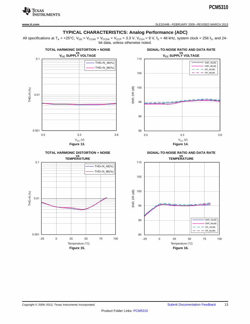
Figure 13. Figure 14.
TOTAL HARMONIC DISTORTION + NOISE SIGNAL-TO-NOISE RATIO AND DATA RATEvs vs
TEMPERATURE TEMPERATURE
Figure 15. Figure 16.
Copyright © 2009–2013, Texas Instruments Incorporated Submit Documentation Feedback 13
Product Folder Links: PCM5310

0.01
0.1
1
10
10 20 30 40 50 60 70
Output Power (mW)
TH
D+
N (
%)
THD+N_0dB(%)
THD+N_6dB(%)
THD+N_12dB(%)
0.01
0.1
1
10
10 15 20 25 30 35 40
Output Power (mW)
TH
D+
N (
%)
THD+N_0dB(%)
THD+N_6dB(%)
THD+N_12dB(%)
0.01
0.1
1
10
100
10 20 30 40 50 60 70 80 90 100
Output Power (mW)
TH
D+
N (
%)
THD+N_3V(%)
THD+N_3.3V(%)
THD+N_3.6V(%)
0.01
0.1
1
10
100
10 20 30 40 50 60
Output Power (mW)
TH
D+
N (
%)
THD+N_3V(%)
THD+N_3.3V(%)
THD+N_3.6V(%)
PCM5310
SLES244B –FEBRUARY 2009–REVISED MARCH 2013 www.ti.com
TYPICAL CHARACTERISTICS: Analog Performance (Headphone)All specifications at TA = +25°C, VDD = VCCAD = VCCDA = VCCP = 3.3 V, VCCH = 9 V, fS = 48 kHz, system clock = 256 fS, and 24-
bit data, unless otherwise noted.
TOTAL HARMONIC DISTORTION + NOISE TOTAL HARMONIC DISTORTION + NOISEvs vs
OUTPUT POWER OUTPUT POWER(48 kHz, 16 Ω) (48 kHz, 32 Ω)
Figure 17. Figure 18.
TOTAL HARMONIC DISTORTION + NOISE TOTAL HARMONIC DISTORTION + NOISEvs vs
OUTPUT POWER OUTPUT POWER(48 kHz, 0 dB, 6 dB, 12 dB, 16 Ω) (48 kHz, 0 dB, 6 dB, 12 dB, 32 Ω)
Figure 19. Figure 20.
14 Submit Documentation Feedback Copyright © 2009–2013, Texas Instruments Incorporated
Product Folder Links: PCM5310

-140
-120
-100
-80
-60
-40
-20
0
20
0 20 40 60 80 100 120
Frequency (kHz)
Am
plit
ude (
dB
)
-140
-120
-100
-80
-60
-40
-20
0
0 5 10 15 20
Frequency (kHz)
Am
plit
ude (
dB
)
-140
-120
-100
-80
-60
-40
-20
0
0 5 10 15 20
Frequency (kHz)
Am
plit
ude (
dB
)
-140
-120
-100
-80
-60
-40
-20
0
0 5 10 15 20
Frequency (kHz)
Am
plit
ude (
dB
)
PCM5310
www.ti.com SLES244B –FEBRUARY 2009–REVISED MARCH 2013
TYPICAL CHARACTERISTICS: Output Spectrum (DAC)All specifications at TA = +25°C, VDD = VCCAD = VCCDA = VCCP = 3.3 V, VCCH = 9 V, fS = 48 kHz, system clock = 256 fS, and 24-
bit data, unless otherwise noted.
AMPLITUDE AMPLITUDEvs vs
FREQUENCY FREQUENCY(0 dB, 0 kHz to 20 kHz) (–60 dB, 0 kHz to 20 kHz)
Figure 21. Figure 22.
AMPLITUDE AMPLITUDEvs vs
FREQUENCY FREQUENCY(Zero Data Input, 0 kHz to 20 kHz) (Zero Data Input, 0 kHz to 130 kHz)
Figure 23. Figure 24.
Copyright © 2009–2013, Texas Instruments Incorporated Submit Documentation Feedback 15
Product Folder Links: PCM5310

-140
-120
-100
-80
-60
-40
-20
0
20
0 5 10 15 20
Frequency (kHz)
Am
plit
ude (
dB
)
-140
-120
-100
-80
-60
-40
-20
0
20
0 5 10 15 20
Frequency (kHz)
Am
plit
ude (
dB
)-140
-120
-100
-80
-60
-40
-20
0
20
0 5 10 15 20
Frequency (kHz)
Am
plit
ude (
dB
)
PCM5310
SLES244B –FEBRUARY 2009–REVISED MARCH 2013 www.ti.com
TYPICAL CHARACTERISTICS: Output Spectrum (ADC)All specifications at TA = +25°C, VDD = VCCAD = VCCDA = VCCP = 3.3 V, VCCH = 9 V, fS = 48 kHz, system clock = 256 fS, and 24-
bit data, unless otherwise noted.
AMPLITUDE AMPLITUDEvs vs
FREQUENCY FREQUENCY(0 dB, 0 kHz to 20 kHz) (–60 dB, 0 kHz to 20 kHz)
Figure 25. Figure 26.
AMPLITUDEvs
FREQUENCY(Zero Data Input, 0 kHz to 20 kHz)
Figure 27.
16 Submit Documentation Feedback Copyright © 2009–2013, Texas Instruments Incorporated
Product Folder Links: PCM5310

1L-M
UX
1R
-MU
X2L-M
UX
2R
-MU
X
PGA-AD2L
PGA-AD1L
PGA-AD1R
PGA-AD2R
ADC-1L
ADC-1R
ADC-2L
ADC-2R
AIN1L
AIN2L
AIN3L
AIN4L
AIN5L
AIN6L
AIN1R
AIN2R
AIN3R
AIN4R
AIN5R
AIN6R
PCM5310
www.ti.com SLES244B –FEBRUARY 2009–REVISED MARCH 2013
DETAILED DESCRIPTION
ANALOG INPUTS
The PCM5310 includes a four-channel analog-to-digital converter (ADC) with a programmable gain amplifier(PGA) and six stereo analog inputs with a 2-VRMS input. Pins AIN1L/1R to AIN6L/6R are connected to the ADCleft (L) or right ®) channel through the analog multiplexer (mux) and PGA, as shown in Figure 28. If the analoginput voltage level is less than 2 VRMS, it can be amplified by using the PGA. The gain level can be set to 9 dB,6 dB, or 3 dB. The descriptions for the analog input registers are shown in Table 1.
Figure 28. Analog Inputs
Table 1. Analog Input Registers
REGISTER DESCRIPTION REGISTER NUMBER REGISTER BITS
Analog input mux selection for ADC1L/1R 20 AX1R[2:0], AX1L[2:0]
Analog input mux selection for ADC2L/2R 21 AX2R[2:0], AX2L[2:0]
Analog input gain control for ADC1L/1RW 22 AG1R[1:0], AG1L[1:0]
Analog input gain control for ADC2L/2R 23 AG2R[1:0], AG2L[1:0]
Copyright © 2009–2013, Texas Instruments Incorporated Submit Documentation Feedback 17
Product Folder Links: PCM5310
DAC-1L
MU
X-LO
1L
PGA-L01L
AIN1L
AIN2L
AIN3L
AIN4L
AIN5L
AIN6L
AIN1R
AIN2R
AIN3R
AIN4R
AIN5R
AIN6R
PGA-L01R
PGA-L02L
PGA-L02R
PGA-HPOL
PGA-HPOR
DAC-1R
DAC-2L
DAC-2R
HP
HP
MU
X-LO
1R
MU
X-LO
2L
MU
X-LO
2R
MU
X-H
PO
LM
UX
-HP
OR
PCM5310
SLES244B –FEBRUARY 2009–REVISED MARCH 2013 www.ti.com
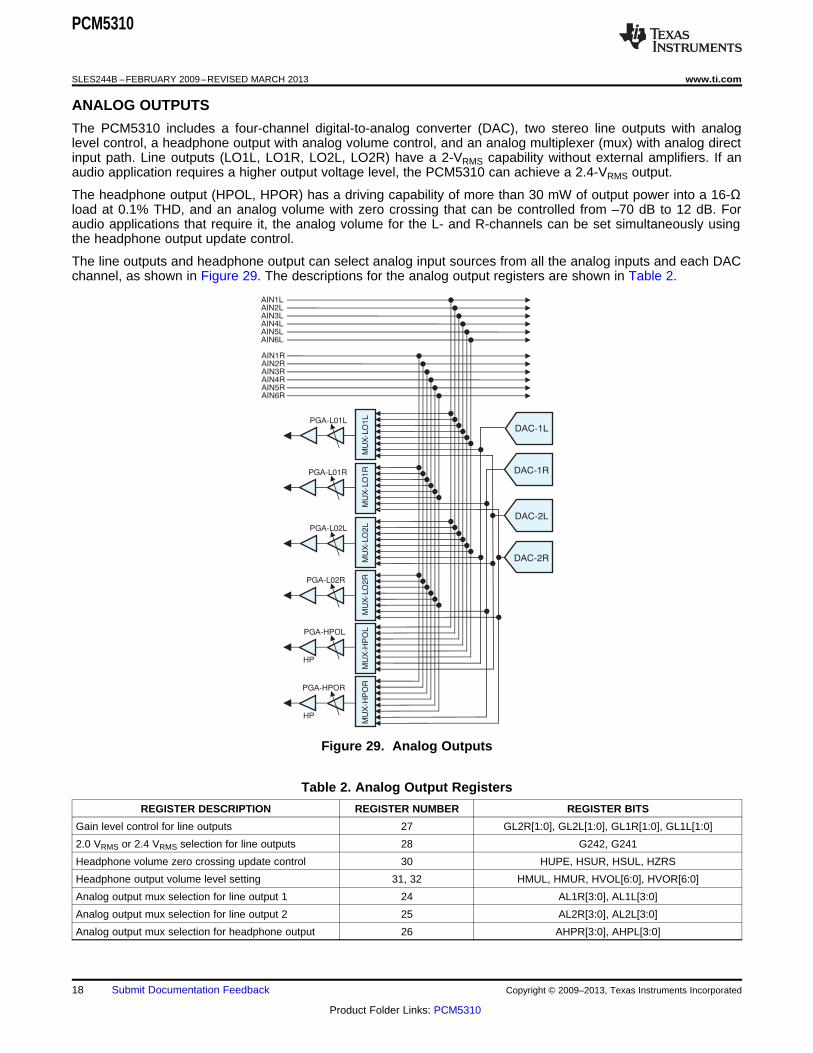
ANALOG OUTPUTS
The PCM5310 includes a four-channel digital-to-analog converter (DAC), two stereo line outputs with analoglevel control, a headphone output with analog volume control, and an analog multiplexer (mux) with analog directinput path. Line outputs (LO1L, LO1R, LO2L, LO2R) have a 2-VRMS capability without external amplifiers. If anaudio application requires a higher output voltage level, the PCM5310 can achieve a 2.4-VRMS output.
The headphone output (HPOL, HPOR) has a driving capability of more than 30 mW of output power into a 16-Ωload at 0.1% THD, and an analog volume with zero crossing that can be controlled from –70 dB to 12 dB. Foraudio applications that require it, the analog volume for the L- and R-channels can be set simultaneously usingthe headphone output update control.
The line outputs and headphone output can select analog input sources from all the analog inputs and each DACchannel, as shown in Figure 29. The descriptions for the analog output registers are shown in Table 2.
Figure 29. Analog Outputs
Table 2. Analog Output Registers
REGISTER DESCRIPTION REGISTER NUMBER REGISTER BITS
Gain level control for line outputs 27 GL2R[1:0], GL2L[1:0], GL1R[1:0], GL1L[1:0]
2.0 VRMS or 2.4 VRMS selection for line outputs 28 G242, G241
Headphone volume zero crossing update control 30 HUPE, HSUR, HSUL, HZRS
Headphone output volume level setting 31, 32 HMUL, HMUR, HVOL[6:0], HVOR[6:0]
Analog output mux selection for line output 1 24 AL1R[3:0], AL1L[3:0]
Analog output mux selection for line output 2 25 AL2R[3:0], AL2L[3:0]
Analog output mux selection for headphone output 26 AHPR[3:0], AHPL[3:0]
18 Submit Documentation Feedback Copyright © 2009–2013, Texas Instruments Incorporated
Product Folder Links: PCM5310

SCK1 to 6
Low
High
0.8 V
2.0 V
tSCL
tSCH
tSCY
PCM5310
www.ti.com SLES244B –FEBRUARY 2009–REVISED MARCH 2013
SYSTEM CLOCK INPUT, OUTPUT, AND fS AUTOMATIC DETECTION
The PCM5310 has six system clock input ports: SCK1, SCK2, SCK3, SCK4, SCK5, and SCK6. Each input portcan receive an independent clock at various frequencies. These ports are used for the internal clock of the digitalfilters and delta-sigma modulators, which are combined into a single common audio clock. The PCM5310automatically detects the input clock rate at 128 fS, 192 fS, 256 fS, 384 fS, 512 fS or 768 fS (where fS is the audiosampling rate); if necessary, automatic clock rate detection can be disabled. The descriptions for the systemclock input, output, and fS automatic detection registers are shown in Table 3. Table 4 shows the frequency ofthe common audio clock. Figure 30 and Table 5 shows the timing requirements for the system clock input.
Table 3. System Clock Input, Output, and fS Automatic Detection Registers
REGISTER DESCRIPTION REGISTER NUMBER REGISTER BITS
Master or slave with fS detection for DAC12 44 DMS12[3:0]
Audio interface format for DAC12 44 DFM12[1:0]
Master or slave with fS detection for DAC34 54 DMS34[3:0]
Audio interface format for DAC34 54 DFM34[1:0]
Master or slave with fS detection for ADC12 84 AMS12[3:0]
Audio interface format for ADC12 84 AFM12[1:0]
Master or slave with fS detection for ADC34 94 AMS34[3:0]
Audio interface format for ADC34 94 AFM34[1:0]
SCK6 clock output selection 07 PSC6[2:0]
Table 4. System Clock Frequencies for the Common Audio Clock
SAMPLING SYSTEM CLOCK FREQUENCY (MHz)FREQUENCY
(kHz) 128 fS(1) 192 fS
(1) 256 fS 384 fS 512 fS 768 fS
32 4.0960 6.1440 8.1920 12.2880 16.3840 24.5760
44.1 5.6488 8.4672 11.2896 16.9344 22.5792 33.8688
48 6.1440 9.2160 12.2880 18.4320 24.5760 36.8640
88.2 11.2896 16.9344 22.5792 33.8688 Not supported Not supported
96 12.2880 18.4320 24.5760 36.8640 Not supported Not supported
176.4 (1) 22.5792 33.8688 Not supported Not supported Not supported Not supported
192 (1) 24.5760 36.8640 Not supported Not supported Not supported Not supported
(1) This sampling frequency and system clock frequency are supported only for the DAC.
Figure 30. System Clock Input Timing
Table 5. Timing Characteristics for Figure 30
PARAMETER MIN MAX UNIT
tSCY System clock cycle time 25 ns
tSCH System clock high time 0.4 tSCY ns
tSCL System clock low time 0.4 tSCY ns
System clock duty cycle 40 60 %
Copyright © 2009–2013, Texas Instruments Incorporated Submit Documentation Feedback 19
Product Folder Links: PCM5310

VDD
Power-On Reset
2.2 V Typical
(1.6 V to 2.8 V)
0 s (min)RSTB
I C Setting2
1 ms (min)
Power-Up for ADCs and DACs(1)
SCKx
Internal Reset for
ADCs and DACs
Clock Input
1.6 V Typical
(1.0 V to 2.0 V)
Clock Input Clock Input
I C Setting is Effective2
1024 Clocks
PCM5310
SLES244B –FEBRUARY 2009–REVISED MARCH 2013 www.ti.com
POWER ON/OFF RESET
The power-on reset (POR) circuit generates a reset signal at typically 2.2 V; this circuit does not depend on theother power supplies: VCCDA, VCCAD, VCCH, and VCCP. The internal circuit is cleared to default status, then allanalog and digital outputs have no signal. It is recommended to turn the device on and off as shown in Figure 31,in order to avoid loud, audible pop noises when powering the device on or off.
(1) RSTB is active low. 100 ns (minimum) is needed for an effective reset to the internal circuit.
Figure 31. Power On/Off Reset
20 Submit Documentation Feedback Copyright © 2009–2013, Texas Instruments Incorporated
Product Folder Links: PCM5310
PCM5310
www.ti.com SLES244B –FEBRUARY 2009–REVISED MARCH 2013
REGISTER RESET AND SYSTEM RESET (Register 01)
Register reset (MRST) clears all register data to the default setting. The MRST register is automatically set to '1'after the reset.
System reset (SRST) clears all internal circuits, including all register data, to default status simultaneously. TheSRST register is automatically set to '1' after the reset.
Note that the PCM5310 may have audible pop noises on the analog and digital outputs when enabling MRSTand SRST.
The descriptions for the register reset and system reset registers are shown in Table 6.
Table 6. Reset Registers
REGISTER DESCRIPTION REGISTER NUMBER REGISTER BITS
Reset register data only 01 MRST
Reset for all circuits including register data 01 SRST
RSTB Control
Taking RSTB (pin 58) from high to low clears all internal circuits to default status. If an application does notrequire reset control, RSTB should be connected with an RC passive delay circuit to the digital power supply(VDD).
Note that the PCM5310 may have audible pop noises on the analog and digital outputs when enabling RSTB.
The RSTB control status descriptions are shown in Table 6.
Table 7. RSTB Control
RSTB (PIN 58) STATUS DESCRIPTION
Low Reset all circuits including register data
High Reset release
Copyright © 2009–2013, Texas Instruments Incorporated Submit Documentation Feedback 21
Product Folder Links: PCM5310

VDD, VCCP,
VCCAD, VCCDA
VCCH (9 V)
I C Register Setting2
Analog Output(1)
Digital Output
75 ms to 2000 ms(2)37.5 ms to 1000 ms
Half of
Power-Supply
Voltage
Recommended
Power-On
Sequence
Recommended
Power-Off
Sequence
PCM5310
SLES244B –FEBRUARY 2009–REVISED MARCH 2013 www.ti.com
POWER-SUPPLY SEQUENCE AND POWER ON/OFF SEQUENCE
In order to reduce audible pop noise, a register setting sequence is required after turning on all power suppliesand before turning off all power supplies. Any modules that are not used in the application or system should bepowered down after the recommended power-on sequence. Before the power-off sequence, all modules shouldbe in a power-on state. The recommended power-supply sequence is shown in Figure 32. The recommendedregister settings are shown in Table 8 and Table 9.
(1) Ramp up/down time for the analog output can be changed through the register setting (see Register 18, PDTM[2:0]).
(2) A 1.0-µF capacitor should be connected to the VCOMAD and VCOMDA pins.
Figure 32. Recommended Power On/Off Sequence
Table 8. Recommended Register Settings When Powered On
REGISTER SETTING
STEP ADDRESS DATA DESCRIPTION
1 — — Turn on all power supplies
2 11 00 Analog bias power up
3 1F 49 Headphone output L-channel mute disable and level (–42 dB) setting (1)
4 20 49 Headphone output R-channel mute disable and level (–42 dB) setting (1)
5 1E B0 Headphone volume update control
6 1B 00 Line output gain (0 dB) control from DAC (1)
7 1C 00 Line output 2 VRMS and 2.4 VRMS mode select
8 2A FF DAC12 L-channel digital attenuation level (0 dB) setting (1)
9 2B FF DAC12 R-channel digital attenuation level (0 dB) setting (1)
10 29 00 DAC12 digital mute setting and digital gain boost
11 28 B1 DAC12 digital attenuation/mute control and zero crossing enable
12 34 FF DAC34 L-channel digital attenuation level (0 dB) setting (1)
13 35 FF DAC34 R-channel digital attenuation level (0 dB) setting (1)
14 33 00 DAC34 digital mute setting and digital gain (0 dB) boost
15 32 B1 DAC34 digital attenuation/mute control and zero crossing enable
16 52 D5 ADC12 L-channel digital attenuation level (0 dB) setting (1)
17 53 D5 ADC12 R-channel digital attenuation level (0 dB) setting (1)
(1) Any level is acceptable for volume, gain, and attenuation. The level should be resumed by register data recorded when the systempowers off.
22 Submit Documentation Feedback Copyright © 2009–2013, Texas Instruments Incorporated
Product Folder Links: PCM5310

PCM5310
www.ti.com SLES244B –FEBRUARY 2009–REVISED MARCH 2013
Table 8. Recommended Register Settings When Powered On (continued)
REGISTER SETTING
STEP ADDRESS DATA DESCRIPTION
18 51 00 ADC12 digital mute disable
19 50 01 ADC12 digital attenuation/mute control and zero crossing enable
20 5C D7 ADC34 L-channel digital attenuation level (0 dB) setting (1)
21 5D D7 ADC34 R-channel digital attenuation level (0 dB) setting (1)
22 5B 00 ADC34 digital mute disable
23 5A 01 ADC34 digital attenuation/mute control and zero crossing enable
24 18 77 Line output 1 L-/R-channel mux select
25 19 00 Line output 2 L-/R-channel mux select
26 1A 88 Headphone output L-/R-channel mux select
27 14 11 ADC12 analog input mux select (AIN1L/R) (2)
28 15 22 ADC34 analog input mux select (AIN2L/R) (2)
29 16 00 ADC12 analog input gain level (0 dB) setting (1)
30 17 00 ADC34 analog input gain level (0 dB) setting (1)
31 65 98 Audio interface (LRCKx/BCKx) PORT-1 and PORT-2 setting (ADC12/34, master) (3)
32 66 98 Audio interface (DATAx) PORT-1 and PORT-2 setting (DATA output of ADC12/34) (3)
33 67 10 Audio interface (SCKx) PORT-1 and PORT-2 setting (input of SCK1/2) (4)
Audio interface (LRCKx/BCKx) PORT-3 and PORT-4 setting (input of LRCK3/4,34 68 32 BCK3/4) (4)
35 69 32 Audio interface (DATAx) PORT-3 and PORT-4 setting (input of DATA3/4) (4)
36 6A 32 Audio interface (SCKx) PORT-3 and PORT-4 setting (input of SCK3/4) (4)
Audio interface (LRCKx/BCKx) PORT-5 and PORT-6 setting (input of LRCK3/4,37 6B 54 BCK3/4) (4)
38 6C 54 Audio interface (DATAx) PORT-5 and PORT-6 setting (input of DATA5/6) (4)
39 6D 54 Audio interface (SCKx) PORT-5 and PORT-6 setting (input of SCK5/6) (4)
40 6E 43 DAC12 and DAC34 LRCK/BCK select (4)
41 6F 43 DAC12 and DAC34 DATA select (4)
42 70 43 DAC12 and DAC34 SCK select (4)
43 74 89 ADC12 and ADC34 LRCK/BCK select (ADC12/34, master) (4)
44 75 10 ADC12 and ADC34 SCK select (4)
45 76 76 GPIO control or GPIO1 and GPIO2 audio data select
46 2C 80 DAC12 audio interface and master/slave select (5)
47 36 80 DAC34 audio interface and master/slave select (5)
48 54 40 ADC12 audio interface and master/slave select (master, 256 fS) (5)
49 5E 40 ADC34 audio interface and master/slave select (master, 256 fS) (5)
50 12 11 Analog back-end and front-end power-up
51 2E 00 DAC12 power-up
52 38 00 DAC34 power-up
53 55 00 ADC12 power-up
54 5F 00 ADC34 power-up
55 12 01 Common voltage (VCOM) power-up and ramp up/down time setting
(2) Any input terminals are acceptable for input of ADC12 and ADC34.(3) These settings are not required if application does not use audio interface mux and bypass selection.(4) These settings are not required if application does not use audio interface mux and bypass selection.(5) These settings are not required if application uses slave mode for audio interface and SCK automatic fS detection.
Copyright © 2009–2013, Texas Instruments Incorporated Submit Documentation Feedback 23
Product Folder Links: PCM5310

PCM5310
SLES244B –FEBRUARY 2009–REVISED MARCH 2013 www.ti.com
Table 9. Recommended Register Setting When Powered Off
REGISTER SETTING
STEP ADDRESS DATA DESCRIPTION
1 18 00 Line output1 L- and R-channel mux select
2 19 00 Line output2 L- and R-channel mux select
3 1A 00 Headphone output L- and R-channel mux select
4 14 00 ADC12 analog input mux select
5 15 00 ADC34 analog input mux select
6 12 11 Common voltage (VCOM) power-down and ramp up/down time setting
7 55 80 ADC12 power-down
8 5F 80 ADC34 power-down
9 2E 80 DAC12 power-down
10 38 80 DAC34 power-down
11 12 71 Analog back-end and front-end power-down
12 11 80 Analog bias power-down
13 — — Turn off all power supplies
24 Submit Documentation Feedback Copyright © 2009–2013, Texas Instruments Incorporated
Product Folder Links: PCM5310

PCM5310
www.ti.com SLES244B –FEBRUARY 2009–REVISED MARCH 2013
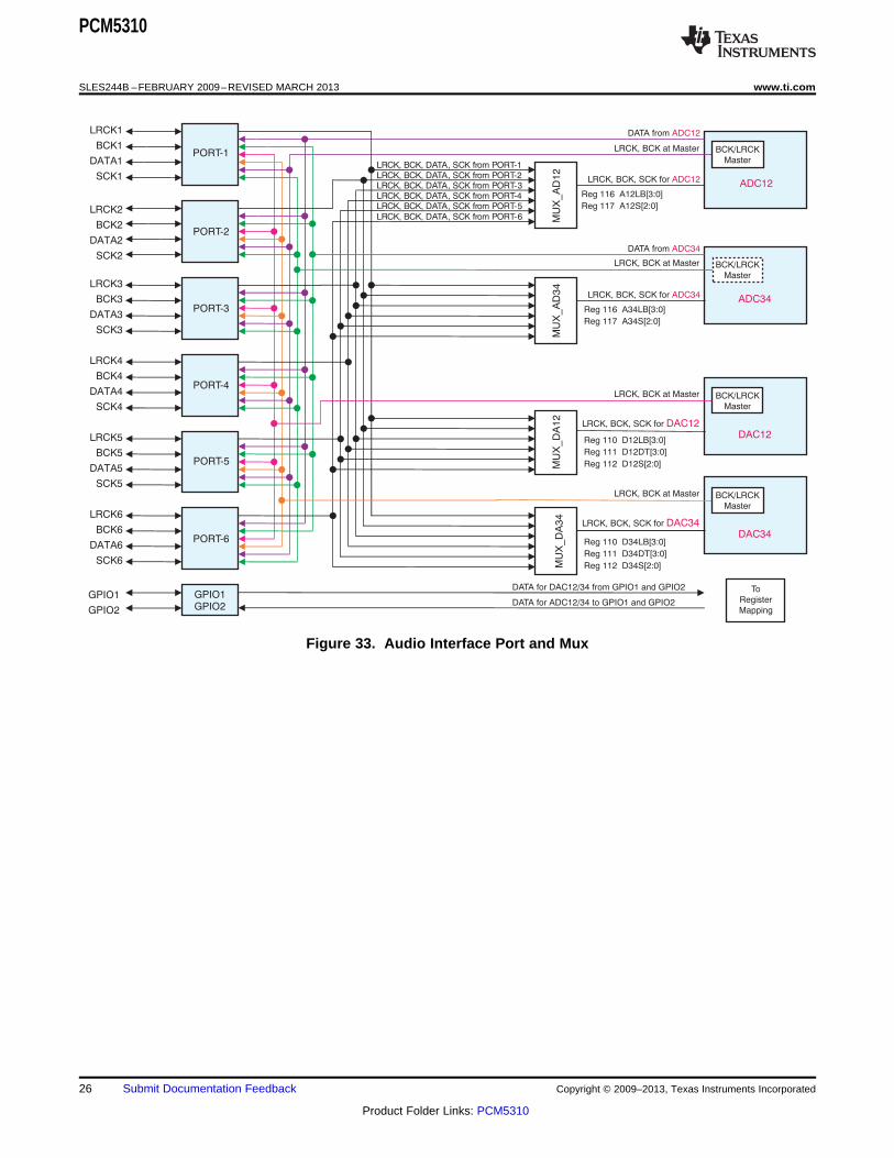
AUDIO SERIAL INTERFACE
The PCM5310 has six audio interface ports: SCKx, BCKx, LRCKx, and DATAx (bidirectional). Each port or signalcan be connected to any ADC or DAC. If an audio system application wants to bypass an audio signal, thePCM5310 can bypass from any port to any port. Refer to Figure 33 for a diagram of the of the audio interfaceport and mux. See Figure 47 to Figure 52 for detailed diagrams of PORT-1 to PORT-6.
The audio interface consists of LRCKs, BCKs, and DATAs. The sampling rate (fS), left channel and right channeldata are present on the LRCKs. The DATAs receive the serial audio data from the interpolation filter for the DAC,and the DATAs transmit the serial data to the decimation filter. The BCKs are used to receive and transmit theserial audio data on the DATAs by high-to-low transition. The BCKs and LRCKs should be synchronized with thesystem clocks, SCKs. The PCM5310 operates with the LRCKs/BCKs synchronized with the SCKs; however, thePCM5310 does not need a specific phase between the BCKs/LRCKs and the SCKs. Each audio interface portcan select either the master or slave mode, and generate the LRCKs and BCKs from the SCKs in master mode.The descriptions for the audio serial interface registers are shown in Table 6.
Table 10. Audio Serial Interface Registers
REGISTER DESCRIPTION REGISTER NUMBER REGISTER BITS
Master or slave with fS detection for DAC12 44 DMS12[3:0]
Audio interface format for DAC12 44 DFM12[1:0]
Master or slave with fS detection for DAC34 54 DMS34[3:0]
Audio interface format for DAC34 54 DFM34[1:0]
Master or slave with fS detection for ADC12 84 AMS12[3:0]
Audio interface format for ADC12 84 AFM12[1:0]
Master or slave with fS detection for ADC34 94 AMS34[3:0]
Audio interface format for ADC34 94 AFM34[1:0]
LRCK/BCK selection of PORT-1 and PORT-2 101 LBS2[3:0], LBS1[3:0]
DATA selection of PORT-1 and PORT-2 102 DTS2[3:0], DTS1[3:0]
SCK selection of PORT-1 and PORT-2 103 SCS2[2:0], SCS1[2:0]
LRCK/BCK selection of PORT-3 and PORT-4 104 LBS4[3:0], LBS3[3:0]
DATA selection of PORT-3 and PORT-4 105 DTS4[3:0], DTS3[3:0]
SCK selection of PORT-3 and PORT-4 106 SCS4[2:0], SCS3[2:0]
LRCK/BCK selection of PORT-5 and PORT-6 107 LBS6[3:0], LBS5[3:0]
DATA selection of PORT-5 and PORT-6 108 DTS6[3:0], DTS5[3:0]
SCK selection of PORT-5 and PORT-6 109 SCS6[2:0], SCS5[2:0]
LRCK/BCK selection of DAC12 and DAC34 110 D34LB[3:0], D12LB[3:0]
DATA selection of DAC12 and DAC34 111 D34DT[3:0], D12DT[3:0]
SCK selection of DAC12 and DAC34 112 D34S[2:0], D12S[2:0]
LRCK/BCK selection of ADC12 and ADC34 116 A34LB[3:0], A12LB[3:0]
SCK selection of ADC12 and ADC34 117 A34SC[2:0], A12SC[2:0]
GPIO-1 and GPIO-2 audio data selection 118 GP2S[3:0], GP1S[3:0]
Copyright © 2009–2013, Texas Instruments Incorporated Submit Documentation Feedback 25
Product Folder Links: PCM5310
ADC12
ADC34
MU
X_A
D12
PORT-1
LRCK1
BCK1
DATA1
SCK1
LRCK, BCK at Master
GPIO1
GPIO2
DATA for DAC12/34 from GPIO1 and GPIO2
ADC12DATA from
DATA for ADC12/34 to GPIO1 and GPIO2
MU
X_A
D34
MU
X_
DA
12
MU
X_
DA
34
Reg 116 A12LB[3:0]
Reg 117 A12S[2:0]
LRCK, BCK, DATA, SCK from PORT-1LRCK, BCK, DATA, SCK from PORT-2LRCK, BCK, DATA, SCK from PORT-3LRCK, BCK, DATA, SCK from PORT-4LRCK, BCK, DATA, SCK from PORT-5LRCK, BCK, DATA, SCK from PORT-6
LRCK2
BCK2
DATA2
SCK2
LRCK3
BCK3
DATA3
SCK3
LRCK4
BCK4
DATA4
SCK4
LRCK5
BCK5
DATA5
SCK5
LRCK6
BCK6
DATA6
SCK6
GPIO1GPIO2
Reg 116 A34LB[3:0]
Reg 117 A34S[2:0]
Reg 110 D12LB[3:0]
Reg 111 D12DT[3:0]
Reg 112 D12S[2:0]
PORT-2
PORT-3
PORT-4
PORT-5
PORT-6
ADC34DATA from
LRCK, BCK, SCK for ADC12
LRCK, BCK at Master
LRCK, BCK, SCK for ADC34
LRCK, BCK at Master
LRCK, BCK, SCK for DAC12
LRCK, BCK at Master
LRCK, BCK, SCK for DAC34
Reg 110 D34LB[3:0]
Reg 111 D34DT[3:0]
Reg 112 D34S[2:0]
DAC12
DAC34
ToRegisterMapping
BCK/LRCKMaster
BCK/LRCKMaster
BCK/LRCKMaster
BCK/LRCKMaster
PCM5310
SLES244B –FEBRUARY 2009–REVISED MARCH 2013 www.ti.com
Figure 33. Audio Interface Port and Mux
26 Submit Documentation Feedback Copyright © 2009–2013, Texas Instruments Incorporated
Product Folder Links: PCM5310

(a) Right-Justified Data Format; L-Channel = HIGH, R-Channel = LOW
LRCK
BCK
(= 32 f , 48 f , or 64 f )S S S
R-ChannelL-Channel
DATA
LRCK
BCK
(= 32 f , 48 f , or 64 f )S S S
DATA
LRCK
BCK
(= 32 f , 48 f , or 64 f )S S S
DATA
MSB LSB MSB LSB
1/fS
(b) I S Data Format; L-Channel = LOW, R-Channel = HIGH2
L-Channel
MSB LSB
R-Channel
MSB LSB
1/fS
(c) Left-Justified Data Format; L-Channel = HIGH, R-Channel = LOW
R-ChannelL-Channel
MSB LSB MSB LSB
1/fS
PCM5310
www.ti.com SLES244B –FEBRUARY 2009–REVISED MARCH 2013
AUDIO DATA FORMATS AND TIMING
The PCM5310 supports I2S, left-justified, and right-justified data formats with 32 fS, 48 fS, or 64 fS BCK rates fordigital input, and 48 fS or 64 fS BCK rates for the ADC. The data formats are shown in Figure 34 and can beselected through the I2C interface. All formats require binary twos complement, MSB first audio data. The defaultformat is 16- to 24-bits I2S. Figure 35 and Figure 36 show detailed timing diagrams. The descriptions for theaudio interface data format registers are shown in Table 11.
Table 11. Audio Interface Data Format Registers
REGISTER DESCRIPTION REGISTER NUMBER REGISTER BITS
Audio interface format for DAC12 44 DFM12[1:0]
Audio interface format for DAC34 54 DFM34[1:0]
Audio interface format for ADC12 84 AFM12[1:0]
Audio interface format for ADC34 94 AFM34[1:0]
Figure 34. Audio Data Input and Output Formats
Copyright © 2009–2013, Texas Instruments Incorporated Submit Documentation Feedback 27
Product Folder Links: PCM5310

DATAx(1)
(Output Mode) 0.5 VDD
1.4 VLRCKx
(Input)
BCKx
(Input) 1.4 V
DATAx
(Input Mode)1.4 V
tBCH tBCL
tBCY tLRH tLRS
tDIS tDIH
tDOD
PCM5310
SLES244B –FEBRUARY 2009–REVISED MARCH 2013 www.ti.com
(1) Load capacitance of output is 20 pF.
Figure 35. Audio Interface Timing (Slave Mode)
Table 12. Timing Requirements for Figure 35
PARAMETER MIN MAX UNIT
tBCY BCKx cycle time 75 ns
tBCH BCKx pulse width high 35 ns
tBCL BCKx pulse width low 35 ns
tLRS LRCKx set-up time to BCKx rising edge 15 ns
tLRH LRCKx hold time to BCKx rising edge 10 ns
tDIS DATAx setup time to BCKx rising edge 10 ns
tDIH DATAx hold time to BCKx rising edge 10 ns
tDOD DATAx delay time from BCKx falling edge 0 30 ns
28 Submit Documentation Feedback Copyright © 2009–2013, Texas Instruments Incorporated
Product Folder Links: PCM5310
0.5 VDD
0.5 VDD
LRCKx
(Output)
BCKx
(Output) 0.5 VDD
1.4 V
tBCH
tDOD
DATAx(1)
(Output Mode)
DATAx
(Input Mode)
tBCL
tBCY tLRD
tDIS tDIH
PCM5310
www.ti.com SLES244B –FEBRUARY 2009–REVISED MARCH 2013
(1) Load capacitance of output is 20 pF.
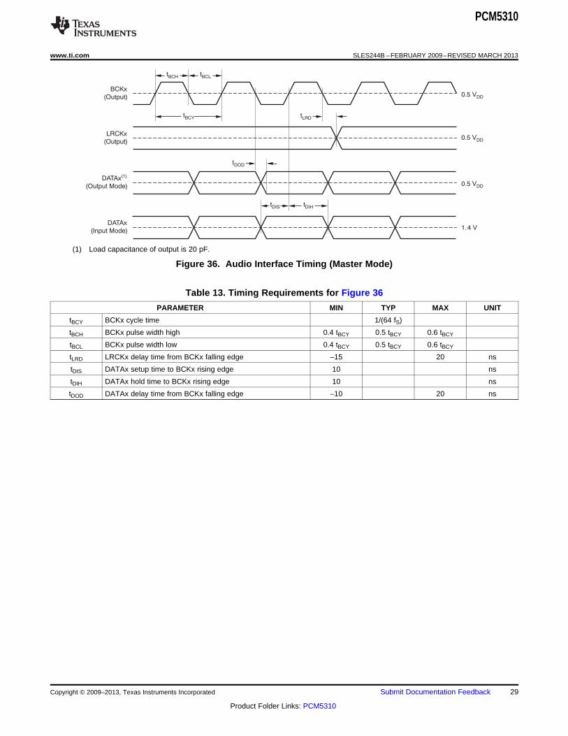
Figure 36. Audio Interface Timing (Master Mode)
Table 13. Timing Requirements for Figure 36
PARAMETER MIN TYP MAX UNIT
tBCY BCKx cycle time 1/(64 fS)
tBCH BCKx pulse width high 0.4 tBCY 0.5 tBCY 0.6 tBCY
tBCL BCKx pulse width low 0.4 tBCY 0.5 tBCY 0.6 tBCY
tLRD LRCKx delay time from BCKx falling edge –15 20 ns
tDIS DATAx setup time to BCKx rising edge 10 ns
tDIH DATAx hold time to BCKx rising edge 10 ns
tDOD DATAx delay time from BCKx falling edge –10 20 ns
Copyright © 2009–2013, Texas Instruments Incorporated Submit Documentation Feedback 29
Product Folder Links: PCM5310

ADC-1L
PGA-AD1L
Decimation
FilterHPF
ATT
MUTE
ADC-1R
PGA-AD1R
Decimation
FilterHPF
ATT
MUTE
ADC-2L
PGA-AD2L
Decimation
FilterHPF
ATT
MUTE
ADC-2R
PGA-AD2R
Decimation
FilterHPF
ATT
MUTE
PCM5310
SLES244B –FEBRUARY 2009–REVISED MARCH 2013 www.ti.com
ADC AND FILTER
The analog-to-digital converter (ADC) and digital filter include a delta-sigma modulator, decimation filter, high-pass filter (HPF), digital gain control, digital attenuation control, and digital soft mute, as shown in Figure 37. TheHPF eliminates dc offset of the ADC analog section with 0.91 Hz as the cutoff frequency at a 48-kHz samplingrate. The digital gain or attenuation control can be adjusted from 20 dB to –100 dB in 0.5-dB steps. Thedescriptions for the ADC and filter registers are shown in Table 14.
Figure 37. ADCs and Filters
Table 14. ADC and Filter Registers
REGISTER DESCRIPTION REGISTER NUMBER REGISTER BITS
Digital attenuation and gain update control for ADC12 80 A12E, AUC2, AUC1, AZ12
Digital soft mute setting for ADC12 81 AMU2, AMU1
Digital attenuation and gain level setting for ADC12 82, 83 AAT2[7:0], AAT1[7:0]
High-pass filter disable for ADC12 84 HF12
Digital attenuation and gain update control for ADC34 90 A34E, AUC4, AUC3, AZ34
Digital soft mute setting for ADC34 91 AMU4, AMU3
Digital attenuation and gain level setting for ADC34 92, 93 AAT4[7:0], AAT3[7:0]
High-pass filter disable for ADC34 94 HF34
30 Submit Documentation Feedback Copyright © 2009–2013, Texas Instruments Incorporated
Product Folder Links: PCM5310

DAC-1LInterpolation
FilterDEM
DAC-1RInterpolation
FilterDEM
DAC-2LInterpolation
FilterDEM
DAC-2RInterpolation
Filter
ATT
MUTE
GAIN
DEM
ATT
MUTE
GAIN
ATT
MUTE
GAIN
ATT
MUTE
GAIN
PCM5310
www.ti.com SLES244B –FEBRUARY 2009–REVISED MARCH 2013
DAC AND FILTER
The digital-to-analog converter (DAC) and digital filter include a delta-sigma modulator, interpolation filter, de-emphasis filter (DEM), digital gain control, digital attenuation control, digital soft mute, and digital gain boost, asshown in Figure 38. The digital gain or attenuation control can be adjusted from 20 dB to –100 dB in 0.5-dBsteps. To play back low-volume recorded audio data, the digital gain can be used with a boost of either 6 dB,12 dB, or 18 dB selected through the I2C interface. The descriptions for the DAC and filter registers are shown inTable 14.
Figure 38. DACs and Filters
Table 15. DAC and Filter Registers
REGISTER DESCRIPTION REGISTER NUMBER REGISTER BITS
Digital attenuation and gain update control for DAC12 40 D12E, DUC2, DUC1, DZ12
Digital soft mute and boost setting for DAC12 41 DMU2, DMU1, DB12[1:0]
Digital attenuation and gain level setting for DAC12 42, 43 DAT2[7:0], DAT1[7:0]
De-emphasis filter setting for DAC12 45 DM12, DF12[1:0]
Digital attenuation and gain update control for DAC34 50 D34E, DUC4, DUC3, DZ34
Digital soft mute setting for DAC34 51 DMU4, DMU3
Digital attenuation and gain level setting for DAC34 52, 53 DAT4[7:0], DAT3[7:0]
De-emphasis filter setting for DAC34 55 DM34, DF34[1:0]
Copyright © 2009–2013, Texas Instruments Incorporated Submit Documentation Feedback 31
Product Folder Links: PCM5310
GPIOControl
HP Insertion
HP Protection
Zero Flag
Register Out
Logic In/Out
Mu
x
Connect to Port
GPIO1GPIO2
GPIO3
GPIO2
GPIO3
GPIO1
PCM5310
SLES244B –FEBRUARY 2009–REVISED MARCH 2013 www.ti.com
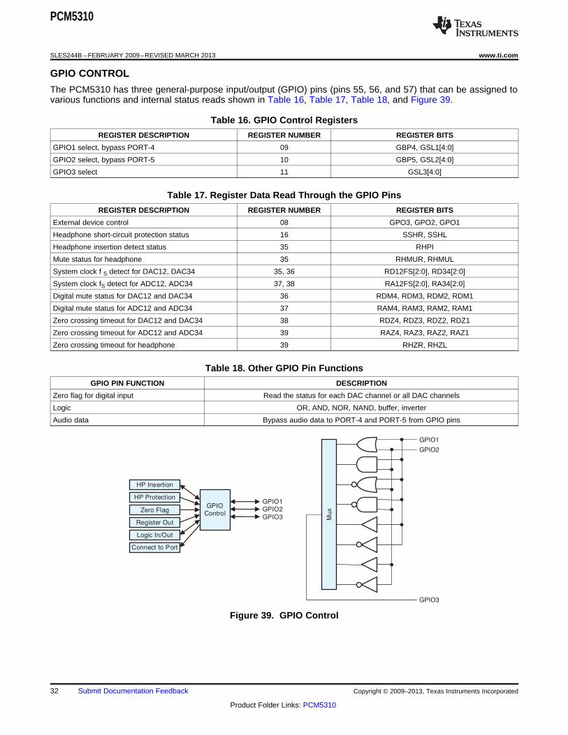
GPIO CONTROL
The PCM5310 has three general-purpose input/output (GPIO) pins (pins 55, 56, and 57) that can be assigned tovarious functions and internal status reads shown in Table 16, Table 17, Table 18, and Figure 39.
Table 16. GPIO Control Registers
REGISTER DESCRIPTION REGISTER NUMBER REGISTER BITS
GPIO1 select, bypass PORT-4 09 GBP4, GSL1[4:0]
GPIO2 select, bypass PORT-5 10 GBP5, GSL2[4:0]
GPIO3 select 11 GSL3[4:0]
Table 17. Register Data Read Through the GPIO Pins
REGISTER DESCRIPTION REGISTER NUMBER REGISTER BITS
External device control 08 GPO3, GPO2, GPO1
Headphone short-circuit protection status 16 SSHR, SSHL
Headphone insertion detect status 35 RHPI
Mute status for headphone 35 RHMUR, RHMUL
System clock f S detect for DAC12, DAC34 35, 36 RD12FS[2:0], RD34[2:0]
System clock fS detect for ADC12, ADC34 37, 38 RA12FS[2:0], RA34[2:0]
Digital mute status for DAC12 and DAC34 36 RDM4, RDM3, RDM2, RDM1
Digital mute status for ADC12 and ADC34 37 RAM4, RAM3, RAM2, RAM1
Zero crossing timeout for DAC12 and DAC34 38 RDZ4, RDZ3, RDZ2, RDZ1
Zero crossing timeout for ADC12 and ADC34 39 RAZ4, RAZ3, RAZ2, RAZ1
Zero crossing timeout for headphone 39 RHZR, RHZL
Table 18. Other GPIO Pin Functions
GPIO PIN FUNCTION DESCRIPTION
Zero flag for digital input Read the status for each DAC channel or all DAC channels
Logic OR, AND, NOR, NAND, buffer, inverter
Audio data Bypass audio data to PORT-4 and PORT-5 from GPIO pins
Figure 39. GPIO Control
32 Submit Documentation Feedback Copyright © 2009–2013, Texas Instruments Incorporated
Product Folder Links: PCM5310

Headphone Jack
HPOL or HPOR
Protection Resistor
Headphone
16 or 32W W
Current
Monitor
Increment
or
Decrement
Counter
Short
or Not
GPIO
Control
Headphone
Amplifier
Enable/Disable
Internal Clock
Internal Resistor
GPIO1, GPIO2, or GPIO3
Detect/Release Time
4096 f : 85.2 ms at f = 48 kHzS S
8192 fS S: 1704 ms at f = 48 kHz
16384 fS S: 340.8 ms at f = 48 kHz
32768 fS S: 681.6 ms at f = 48 kHz
PCM5310
www.ti.com SLES244B –FEBRUARY 2009–REVISED MARCH 2013
HEADPHONE SHORT-CIRCUIT PROTECTION
The PCM5310 has short-circuit protection for each headphone output. The short-circuit status can be read fromthe GPIO pins and the register data can be read through the I2C interface. The short-circuit detection time can beinternally adjusted to avoid the headphone amplifier shutting down when inserting or removing the headphonejack. The descriptions for the headphone and short-circuit protection registers are shown in Table 19. Theheadphone short-circuit protection sequence is shown in Figure 40.
Table 19. Headphone Short-Circuit Protection Registers
REGISTER DESCRIPTION REGISTER NUMBER REGISTER BITS
Headphone short-circuit protection enable/disable 13 SRCR, SHCR, SPDR, SRCL, SHCL, SPDL
Headphone short-circuit protection detect time 14 SDTR[1:0], SDTL[1:0]
Headphone short-circuit protection release time 15 SRTR[1:0], SRTL[1:0]
Headphone short-circuit protection status read 16 SSHR, SSHL
Figure 40. Headphone Short-Circuit Protection Sequence
When the short-circuit protection is enabled, it is recommended to insert a small protection resistor to limit over-current flow. Table 20 shows the headphone output power with a small resistor.
Table 20. Headphone Amplifier Output Power Load
RL = 32 Ω + PROTECTION RESISTOR 32 Ω + 4 Ω 32 Ω + 8 Ω 32 Ω + 16 Ω0.1% THD 28 mW 22 mW 16 mW
10% THD 37 mW 31 mW 22 mW
Copyright © 2009–2013, Texas Instruments Incorporated Submit Documentation Feedback 33
Product Folder Links: PCM5310

HPOR
PGND
Headphone
Jack
DSP
VDD
SDA
SCL
GPIO1, GPIO2, or GPIO3
HPOL
Headphone
Amplifier
GPIO
Control
I C
Register
2
PCM5310
SLES244B –FEBRUARY 2009–REVISED MARCH 2013 www.ti.com
HEADPHONE INSERTION DETECTION
The descriptions for the headphone insertion detection registers are shown in Table 21. The PCM5310 detectsthe insertion status of a headphone plug using the GPIO pins through the register setting and writes the status tothe register, which can be read by the I2C interface. The status can also output to the GPIO pins, as shown inFigure 41.
Table 21. Headphone Insertion Detection Registers
REGISTER DESCRIPTION REGISTER NUMBER REGISTER BITS
GPIO1 selection 09 GSL1[4:0]
GPIO2 selection 10 GSL2[4:0]
GPIO3 selection 11 GSL3[4:0]
Read status for headphone insertion 35 RIPI
Figure 41. Headphone Insertion Detection
34 Submit Documentation Feedback Copyright © 2009–2013, Texas Instruments Incorporated
Product Folder Links: PCM5310

LRCK4
BCK4
DATA4
LRCK5
BCK5
DATA5
PORT-4 DAC12
DAC34
Zero Data
or Not
Zero Data
or Not
Increment
Counter
GPIO Control
GPIO1
GPIO2
GPIO3
Increment
Counter
PORT-5
PCM5310
www.ti.com SLES244B –FEBRUARY 2009–REVISED MARCH 2013
ZERO FLAG DETECTION
The PCM5310 detects continuous zero data input to either DAC12, DAC34, or both DAC12 and DAC34. TheGPIO pins can output the status to an external device by the register setting. The flag changes from low to highwhen the L-and R-channel data are zero after 1024 fS. The descriptions for the zero flag detection registers areshown in Table 22. Figure 42 shows the zero flag detection operation.
Table 22. Zero Flag Registers
REGISTER DESCRIPTION REGISTER NUMBER REGISTER BITS
GPIO1 selection 09 GSL1[4:0]
GPIO2 selection 10 GSL2[4:0]
GPIO3 selection 11 GSL3[4:0]
Figure 42. Zero Flag Detection
AMUTE Control
The PCM5310 has an AMUTE pin (pin 59) that controls the digital and analog mute function linked to Register 19(13h). If these settings are disabled and the AMUTE pin goes from low to high, the PCM5310 holds the digitaland analog mute disabled. If these settings are enabled and the AMUTE pin goes from low to high, thePCM5310 enables digital and analog mute. The mute function set by the AMUTE pin is effective, regardless ofthe setting in Register 19.
Copyright © 2009–2013, Texas Instruments Incorporated Submit Documentation Feedback 35
Product Folder Links: PCM5310

I C Setting2
Clock Source B
Clock Source A
241 8 f (ADC)
1 f (DAC)
(1)
S
S
The digital and analog inputs should be zero data at first. Then use the following setting procedure:
a) Disable zero crossing detection.
b) Enable analog or digital output mute.
c) Change the clock source.
d) Disable the analog or digital mute.
NOTE:
35 f (ADC)
25 f (DAC)S
S
PCM5310
SLES244B –FEBRUARY 2009–REVISED MARCH 2013 www.ti.com
MUTE CONTROL TIMING DURING CLOCK CHANGES
The PCM5310 has six audio interface ports and can change from the current source to another source. However,the analog output or digital output may have an audible pop noise when changing or stopping clocks. It isrecommend to use the mute control with zero data input and waiting time to avoid pop noise and clean up theinternal circuit via I2C. Figure 43 illustrates the details.
Note that the digital and analog inputs should be zero data initially. After that, use the following steps:1. Disable zero crossing detection.2. Enable the analog or digital output mute.3. Change the clock source.4. Disable the analog or digital mute.
(1) Value depends on attenuation level setting in Registers 82, 83, 92, and 93.
Figure 43. Mute Control Timing During Clock Changes
36 Submit Documentation Feedback Copyright © 2009–2013, Texas Instruments Incorporated
Product Folder Links: PCM5310

(2)(1)
AIN1L
AIN2L
I C Setting2
ADC Output
(3)
(4) (4)
PCM5310
www.ti.com SLES244B –FEBRUARY 2009–REVISED MARCH 2013
ANALOG MUX CHANGING TO REDUCE AUDIBLE NOISE
The PCM5310 has an analog multiplexer (mux) that can select six stereo analog inputs. The ADC output mayhave audible noise when selecting without mute control via I2C. It is recommend to use digital soft mute beforechanging the analog input, as shown in Figure 44.
(1) Enable digital soft mute of ADC.
(2) Change analog input source.
(3) Disable digital soft mute of ADC.
(4) Maximum mute time is [241 × 8 fS] seconds; however, this time depends on the wave form if zero crossing isenabled. It is recommended to read the status of this mute from Register 35 to 39 via I2C. Then if the status is high,disable mute.
Figure 44. Analog Mux Changing to Reduce Audible Noise
Copyright © 2009–2013, Texas Instruments Incorporated Submit Documentation Feedback 37
Product Folder Links: PCM5310
SDA
SCL St 1-7
Slave Address
Start
Condition
Stop
Condition
R/W ACK DATA
8 9 1-8 9 1-8 9 Sp
ACK DATA ACK
R/ : Read operation if ‘1’; otherwise, write operation.
ACK: Acknowledgement of a byte if ‘0’.
DATA: 8 bits (1 byte).
W
PCM5310
SLES244B –FEBRUARY 2009–REVISED MARCH 2013 www.ti.com
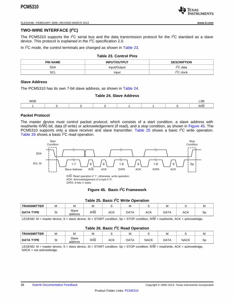
TWO-WIRE INTERFACE (I2C)
The PCM5310 supports the I2C serial bus and the data transmission protocol for the I2C standard as a slavedevice. This protocol is explained in the I2C specification 2.0.
In I2C mode, the control terminals are changed as shown in Table 23.
Table 23. Control Pins
PIN NAME INPUT/OUTPUT DESCRIPTION
SDA Input/Output I2C data
SCL Input I2C clock
Slave Address
The PCM5310 has its own 7-bit slave address, as shown in Table 24.
Table 24. Slave AddressMSB LSB
1 0 0 0 1 1 0 R/W
Packet Protocol
The master device must control packet protocol, which consists of a start condition, a slave address withread/write ®/W) bit, data (if write) or acknowledgement (if read), and a stop condition, as shown in Figure 45. ThePCM5310 supports only a slave receiver and slave transmitter. Table 25 shows a basic I2C write operation.Table 26 shows a basic I2C read operation.
Figure 45. Basic I2C Framework
Table 25. Basic I2C Write OperationTRANSMITTER M M M S M S M S M
SlaveDATA TYPE St R/W ACK DATA ACK DATA ACK Spaddress
LEGEND: M = master device, S = slave device, St = START condition, Sp = STOP condition, R/W = read/write, ACK = acknowledge.
Table 26. Basic I2C Read OperationTRANSMITTER M M M S M S M S M
SlaveDATA TYPE St R/W ACK DATA NACK DATA NACK Spaddress
LEGEND: M = master device, S = slave device, St = START condition, Sp = STOP condition, R/W = read/write, ACK = acknowledge,NACK = not acknowledge.
38 Submit Documentation Feedback Copyright © 2009–2013, Texas Instruments Incorporated
Product Folder Links: PCM5310

PCM5310
www.ti.com SLES244B –FEBRUARY 2009–REVISED MARCH 2013
Write Operation
The master can write to any PCM5310 register in a single access. The master sends a PCM5310 slave addresswith a write bit, a register address, and data. When undefined registers are accessed, the PCM5310 does notsend any acknowledgement. Table 27 shows the framework for a write operation.
Table 27. Framework for Write OperationTRANSMITTER M M M S M S M S M
Slave RegisterDATA TYPE St W ACK ACK Write data ACK Spaddress address
LEGEND: M = master device, S = slave device, St = start condition, Sp = stop condition, W = write, ACK = acknowledge.
Read Operation
The master can read any PCM5310 register. The value of the register address is stored in an indirect indexregister in advance. The master sends the PCM5310 slave address with a read bit after storing the registeraddress. The PCM5310 then transfers the data to the address specified by the index register. Table 28 showsthe framework for a read operation.
Table 28. Framework for Read OperationTRANSMITTER M M M S M S M M M S S M M
Slave Register Slave ReadDATA TYPE St W ACK ACK Sr R ACK NACK Spaddress address address data
LEGEND: M = master device, S = slave device, St = START condition, Sr = repeated START condition, Sp = STOP condition,W = write, R = read, ACK = acknowledge, NACK = not acknowledge.
Copyright © 2009–2013, Texas Instruments Incorporated Submit Documentation Feedback 39
Product Folder Links: PCM5310

SDA
SCL
t(BUF) t(D-SU) t(SDA-R) t(SDA-F) t(P-SU)
t(LOW)
t(D-HD)
t(S-HD)t(SCL-F)
t(SCL-R)
t(RS-SU)
t(RS-HD)
Stop
Condition
Start
Condition
t(SP)
t(HI)
PCM5310
SLES244B –FEBRUARY 2009–REVISED MARCH 2013 www.ti.com
I2C Timing Diagram
Figure 46. I2C Timing
Table 29. Timing Characteristics for Figure 46
PARAMETER I2C SPECIFICATION MIN MAX UNIT
fSCL SCL clock frequency Standard 100 kHz
t(BUF) Bus free time between STOP and START condition Standard 4.7 μs
t(LOW) SCL clock low period Standard 4.7 μs
t(HI) SCL clock high period Standard 4 μs
t(RS-SU) START condition setup time Standard 4.7 μs
t(S-HD) START condition hold time Standard 4 μs
t(D-SU) Data setup time Standard 250 ns
t(D-HD) Data hold time Standard 0 900 ns
t(SCL-R) SCL signal rise time Standard 20 + 0.1 CB 1000 ns
Rise time of SCL signal after a repeated STARTt(SCL-R1) Standard 20 + 0.1 CB 1000 nscondition and after an acknowledge bit
t(SCL-F) SCL signal fall time Standard 20 + 0.1 CB 1000 ns
t(SDA-R) SDA signal rise time Standard 20 + 0.1 CB 1000 ns
t(SDA-F) SDA signal fall time Standard 20 + 0.1 CB 1000 ns
t(P-SU) STOP condition setup time Standard 4 μs
CB Capacitive load for SDA and SCL line 400 pF
t(SP) Suppressed spike pulse duration 25 ns
40 Submit Documentation Feedback Copyright © 2009–2013, Texas Instruments Incorporated
Product Folder Links: PCM5310

PCM5310
www.ti.com SLES244B –FEBRUARY 2009–REVISED MARCH 2013
REGISTER MAP
The mode control register map is shown in Table 30. Each register includes an index (or address) indicated bythe IDX[6:0] bits.
Table 30. Mode Control Register Map
REG HEX DESCRIPTION B7 B6 B5 B4 B3 B2 B1 B0
01 01h Reset function MRST SRST RSV (1) RSV RSV RSV RSV RSV
08 08h GPIO pin output control RSV RSV RSV RSV RSV GPO3 GPO2 GPO1
09 09h GPIO PORT-1 selection RSV RSV RSV GSL1[4:0]
10 0Ah GPIO PORT-2 selection RSV RSV RSV GSL2[4:0]
11 0Bh GPIO PORT-3 selection RSV RSV RSV GSL3[4:0]
12 0Ch Not assigned RSV RSV RSV RSV RSV RSV RSV RSV
13 0Dh Headphone short-circuit protection enable/disable RSV SRCR SHCR SPDR RSV SRCL SHCL SPDL
14 0Eh Headphone short-circuit protection detect time RSV RSV SDTR[1:0] RSV RSV SDTL[1:0]
Headphone short-circuit protection release time, auto15 0Fh RSV SADR SRTR[1:0] RSV SADL SRTL[1:0]control
16 10h Headphone short-circuit protection status read RSV RSV RSV SSHR RSV RSV RSV SSHL
17 11h Power up/down (bias) PBIS RSV RSV RSV RSV PDCF[1:0] PDCS
18 12h Power up/down (analog), power up/down time RSV PABE PAFE PCOM RSV PDTM[2:0]
19 13h Mute control linked to AMUTE pin MD12 MD34 MHPR MHPL ML2R ML2L ML1R ML1L
20 14h Analog input mux selection for ADC12 RSV AX1R[2:0] RSV AX1L[2:0]
21 15h Analog input mux selection for ADC34 RSV AX2R[2:0] RSV AX2L[2:0]
22 16h Analog input gain control for ADC12 RSV RSV AG1R[1:0] RSV RSV AG1L[1:0]
23 17h Analog input gain control for ADC12 RSV RSV AG2R[1:0] RSV RSV AG2L[1:0]
24 18h Analog output mux selection for line output 1 AL1R[3:0] AL1L[3:0]
25 19h Analog output mux selection for line output 2 AL2R[3:0] AL2L[3:0]
26 1Ah Analog output mux selection for headphone output AHPR[3:0] AHPL[3:0]
27 1Bh Gain control for line output GL2R[1:0] GL2L[1:0] GL1R[1:0] GL1L[1:0]
28 1Ch 2.0 VRMS and 2.4 VRMS selection for line output RSV RSV RSV G242 RSV RSV RSV G241
29 1Dh Clock halt detection control RSV RSV RSV RSV RSV RSV ACTH CHDE
30 1Eh Headphone output volume control HUPE RSV HSUR HSUL RSV RSV RSV HZRS
Headphone mute and volume level setting for R-31 1Fh HMUL HVOL[6:0]channel
Headphone mute and volume level setting for L-32 20h HMUR HVOR[6:0]channel
33 21h System clock output disable RSV RSV SC6D SC5D SC4D RSV SC2D SC1D
34 22h LRCK and BCK output disable at master mode RSV RSV LB6D LB5D LB4D LB3D LB2D LB1D
35 23h Read internal flag RSV RD12FS[2:0] RHMR RHML RSV RHPI
36 24h Read internal flag RSV RD34FS[2:0] RDM4 RDM3 RDM2 RDM1
37 25h Read internal flag RSV RA12FS[2:0] RAM4 RAM3 RAM2 RAM1
38 26h Read internal flag RSV RA34FS[2:0] RDZ4 RDZ3 RDZ2 RDZ1
39 27h Read internal flag CGLD RSV RHZR RHZL RAZ4 RAZ3 RAZ2 RAZ1
40 28h Digital attenuation and mute control for DAC12 D12E RSV DUC2 DUC1 RSV RSV RSV DZ12
41 29h Digital gain boost and digital soft mute for DAC12 RSV RSV RSV RSV DB12[1:0] DMU2 DMU1
42 2Ah Digital attenuation level setting for DAC12 L-channel DAT1[7:0]
43 2Bh Digital attenuation level setting for DAC12 R-channel DAT2[7:0]
44 2Ch Master/slave interface format for DAC12 DMS12[3:0] RSV RSV DFM12[1:0]
45 2Dh De-emphasis filter control for DAC12 RSV RSV RSV RSV DM12 RSV DF12[1:0]
46 2Eh Power up/down, oversampling rate control for DAC12 PD12 RSV OV12[1:0] ZR12 RSV RSV RSV
(1) RSV = reserved (write '0' data).
Copyright © 2009–2013, Texas Instruments Incorporated Submit Documentation Feedback 41
Product Folder Links: PCM5310

PCM5310
SLES244B –FEBRUARY 2009–REVISED MARCH 2013 www.ti.com
Table 30. Mode Control Register Map (continued)
REG HEX DESCRIPTION B7 B6 B5 B4 B3 B2 B1 B0
50 32h Digital attenuation and mute control for DAC34 D34E RSV DUC4 DUC3 RSV RSV RSV DZ34
51 33h Digital gain boost and digital soft mute for DAC34 RSV RSV RSV RSV DB34[1:0] DMU4 DMU3
52 34h Digital attenuation level setting for DAC34 L-channel DAT3[7:0]
53 35h Digital attenuation level setting for DAC34 R-channel DAT4[7:0]
54 36h Master/slave interface format for DAC34 DMS34[3:0] RSV RSV DFM34[1:0]
55 37h De-emphasis filter control for DAC34 RSV RSV RSV RSV DM34 RSV DF34[1:0]
56 38h Power up/down, oversampling rate control for DAC34 PD34 RSV OV34[1:0] ZR34 RSV RSV RSV
80 50h Digital attenuation and mute control for ADC12 A12E RSV AUC2 AUC1 RSV RSV RSV AZ12
81 51h Digital soft mute for ADC12 RSV FS12 RSV RSV RSV RSV AMU2 AMU1
82 52h Digital attenuation level setting for ADC12 L-channel AAT1[7:0]
83 53h Digital attenuation level setting for ADC12 R-channel AAT2[7:0]
84 54h Master/slave interface format for ADC12 AMS12[3:0] HF12 RSV AFM12[1:0]
85 55h Power up/down for ADC12 PA12 RSV RSV RSV RSV RSV RSV RSV
90 5Ah Digital attenuation and mute control for ADC34 A34E RSV AUC4 AUC3 RSV RSV RSV AZ34
91 5Bh Digital soft mute for ADC34 RSV FS34 RSV RSV RSV RSV AMU4 AMU3
92 5Ch Digital attenuation level setting for ADC34 L-channel AAT3[7:0]
93 5Dh Digital attenuation level setting for ADC34 R-channel AAT4[7:0]
94 5Eh Master/slave, interface format for ADC34 AMS34[3:0] HF34 RSV AFM34[1:0]
95 5Fh Power up/down for ADC34 PA34 RSV RSV RSV RSV RSV RSV RSV
101 65h LRCK/BCK selection of PORT-1 and PORT-2 LBS2[3:0] LBS1[3:0]
102 66h DATA selection of PORT-1 and PORT-2 DTS2[3:0] DTS1[3:0]
103 67h SCK selection of PORT-1 and PORT-2 RSV SCS2[2:0] RSV SCS1[2:0]
104 68h LRCK/BCK selection of PORT-3 and PORT-4 LBS4[3:0] LBS3[3:0]
105 69h DATA selection of PORT-3 and PORT-4 DTS4[3:0] DTS3[3:0]
106 6Ah SCK selection of PORT-3 and PORT-4 RSV SCS4[2:0] RSV SCS3[2:0]
107 6Bh LRCK/BCK selection of PORT-5 and PORT-6 LBS6[3:0] LBS5[3:0]
108 6Ch DATA selection of PORT-5 and PORT-6 DTS6[3:0] DTS5[3:0]
109 6Dh SCK selection of PORT-5 and PORT-6 RSV SCS6[2:0] RSV SCS5[2:0]
110 6Eh LRCK/BCK selection of DAC12 and DAC34 D34LB[3:0] D12LB[3:0]
111 6Fh DATA selection of DAC12 and DAC34 D34DT[3:0] D12DT[3:0]
112 70h SCK selection of DAC12 and DAC34 RSV D34S[2:0] RSV D12S[2:0]
113 71h Not assigned RSV RSV RSV RSV RSV RSV RSV RSV
114 72h Not assigned RSV RSV RSV RSV RSV RSV RSV RSV
115 73h Not assigned RSV RSV RSV RSV RSV RSV RSV RSV
116 74h LRCK/BCK selection of ADC12 and ADC34 A34LB[3:0] A12LB[3:0]
117 75h SCK selection of ADC12 and ADC34 RSV A34SC[2:0] RSV A12SC[2:0]
118 76h GPIO1 and GPIO2 audio data selection GP2S[3:0] GP1S[3:0]
42 Submit Documentation Feedback Copyright © 2009–2013, Texas Instruments Incorporated
Product Folder Links: PCM5310
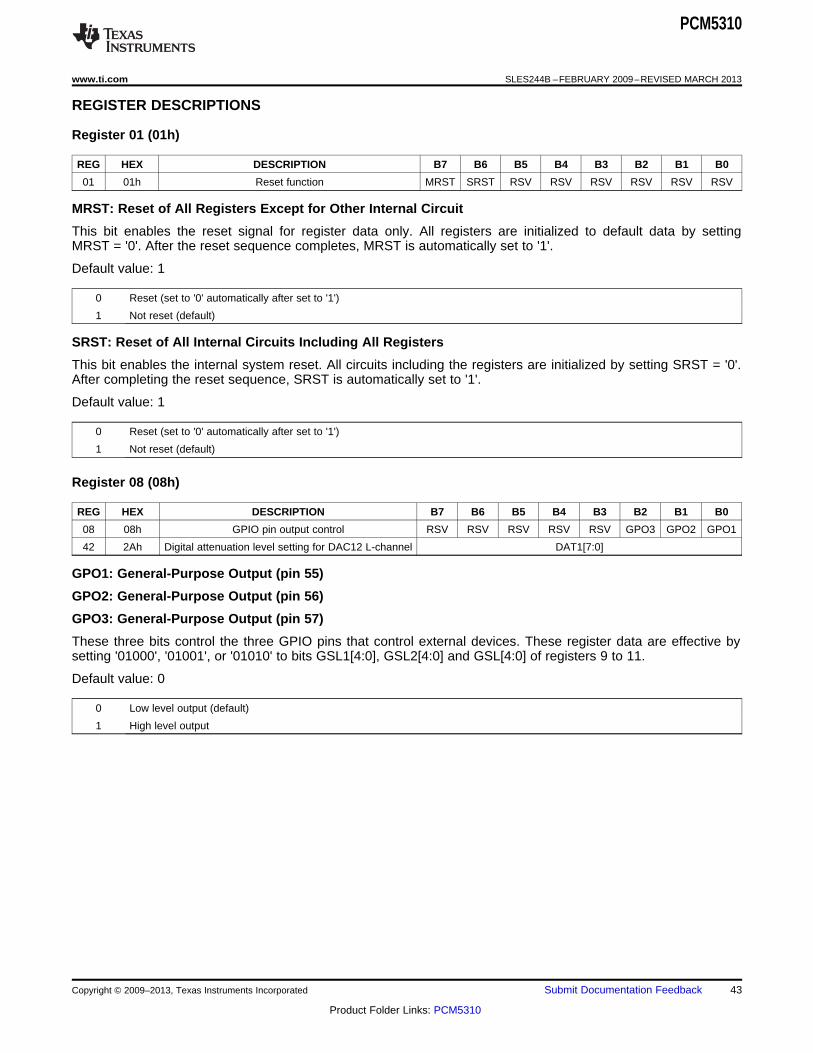
PCM5310
www.ti.com SLES244B –FEBRUARY 2009–REVISED MARCH 2013
REGISTER DESCRIPTIONS
Register 01 (01h)
REG HEX DESCRIPTION B7 B6 B5 B4 B3 B2 B1 B0
01 01h Reset function MRST SRST RSV RSV RSV RSV RSV RSV
MRST: Reset of All Registers Except for Other Internal Circuit
This bit enables the reset signal for register data only. All registers are initialized to default data by settingMRST = '0'. After the reset sequence completes, MRST is automatically set to '1'.
Default value: 1
0 Reset (set to '0' automatically after set to '1')
1 Not reset (default)
SRST: Reset of All Internal Circuits Including All Registers
This bit enables the internal system reset. All circuits including the registers are initialized by setting SRST = '0'.After completing the reset sequence, SRST is automatically set to '1'.
Default value: 1
0 Reset (set to '0' automatically after set to '1')
1 Not reset (default)
Register 08 (08h)
REG HEX DESCRIPTION B7 B6 B5 B4 B3 B2 B1 B0
08 08h GPIO pin output control RSV RSV RSV RSV RSV GPO3 GPO2 GPO1
42 2Ah Digital attenuation level setting for DAC12 L-channel DAT1[7:0]
GPO1: General-Purpose Output (pin 55)
GPO2: General-Purpose Output (pin 56)
GPO3: General-Purpose Output (pin 57)
These three bits control the three GPIO pins that control external devices. These register data are effective bysetting '01000', '01001', or '01010' to bits GSL1[4:0], GSL2[4:0] and GSL[4:0] of registers 9 to 11.
Default value: 0
0 Low level output (default)
1 High level output
Copyright © 2009–2013, Texas Instruments Incorporated Submit Documentation Feedback 43
Product Folder Links: PCM5310

PCM5310
SLES244B –FEBRUARY 2009–REVISED MARCH 2013 www.ti.com
Registers 09-12 (09h-0Ch)
REG HEX DESCRIPTION B7 B6 B5 B4 B3 B2 B1 B0
09 09h GPIO PORT-1 selection RSV RSV RSV GSL1[4:0]
10 0Ah GPIO PORT-2 selection RSV RSV RSV GSL2[4:0]
11 0Bh GPIO PORT-3 selection RSV RSV RSV GSL3[4:0]
12 0Ch Not assigned RSV RSV RSV RSV RSV RSV RSV RSV
GSL1[4:0]: GPO1 Function Selection (pin 55)
GSL2[4:0]: GPO2 Function Selection (pin 56)
GSL3[4:0]: GPO3 Function Selection (pin 57)
The three GPIO pins can be used as an input flag, output flag, and logic function, as shown in Table 31.
Default value: 00000
Table 31. GPIO Functions
GSL1-3[4:0] GSL1[4:0]/GPIO1 GSL2[4:0]/GPIO2 GSL3[4:0]/GPIO3
00000 No assigned and input mode (default) No assigned and input mode (default) No assigned and input mode (default)
00001 Headphone insertion detection input Headphone insertion detection input Headphone insertion detection input
00010 Headphone insertion detection output Headphone insertion detection output Headphone insertion detection output
00011 Headphone short detection status L-channel Headphone short detection status L-channel Headphone short detection status L-channel
00100 Headphone short detection status R-channel Headphone short detection status R-channel Headphone short detection status R-channel
00101 Zero flag output for digital input (DAC12) Zero flag output for digital input (DAC12) Zero flag output for digital input (DAC12)
00110 Zero flag output for digital input (DAC34) Zero flag output for digital input (DAC34) Zero flag output for digital input (DAC34)
00111 Zero flag output for digital input (DAC12 and Zero flag output for digital input (DAC12 and Zero flag output for digital input (DAC12 andDAC34) DAC34) DAC34)
01000 Output register data to GPIO1 pin Output register data to GPIO1 pin Output register data to GPIO1 pin
01001 Output register data to GPIO2 pin Output register data to GPIO2 pin Output register data to GPIO2 pin
01010 Output register data to GPIO3 pin Output register data to GPIO3 pin Output register data to GPIO3 pin
01011 AND logic (GPIO1 = output, GPIO2,3 = input) AND logic (GPIO2 = output, GPIO1,3 = input) AND logic (GPIO2 = output, GPIO1,3 = input)
01100 NAND logic (GPIO1 = output, GPIO2,3 = NAND logic (GPIO2 = output, GPIO1,3 = NAND logic (GPIO2 = output, GPIO1,3 =input) input) input)
01101 OR logic (GPIO1 = output, GPIO2,3 = input) OR logic (GPIO2 = output, GPIO1,3 = input) OR logic (GPIO2 = output, GPIO1,3 = input)
01110 NOR logic (GPIO1 = output, GPIO2,3 = input) NOR logic (GPIO2 = output, GPIO1,3 = input) NOR logic (GPIO2 = output, GPIO1,3 = input)
01111 Buffer logic (GPIO1 = output, GPIO2 = input) Buffer logic (GPIO2 = output, GPIO1 = input) Buffer logic (GPIO2 = output, GPIO1 = input)
10000 Buffer logic (GPIO1 = output, GPIO3 = input) Buffer logic (GPIO2 = output, GPIO3 = input) Buffer logic (GPIO2 = output, GPIO3 = input)
10001 Inverter logic (GPIO1 = output, GPIO2 = input) Inverter logic (GPIO2 = output, GPIO1 = input) Inverter logic (GPIO2 = output, GPIO1 = input)
10010 Inverter logic (GPIO1 = output, GPIO3 = input) Inverter logic (GPIO2 = output, GPIO3 = input) Inverter logic (GPIO2 = output, GPIO3 = input)
Others Reserved Reserved Reserved
44 Submit Documentation Feedback Copyright © 2009–2013, Texas Instruments Incorporated
Product Folder Links: PCM5310

PCM5310
www.ti.com SLES244B –FEBRUARY 2009–REVISED MARCH 2013
Registers 13-16 (0Dh-10h)
REG HEX DESCRIPTION B7 B6 B5 B4 B3 B2 B1 B0
13 0Dh Headphone short-circuit protection enable/disable RSV SRCR SHCR SPDR RSV SRCL SHCL SPDL
14 0Eh Headphone short-circuit protection detect time RSV RSV SDTR[1:0] RSV RSV SDTL[1:0]
Headphone short-circuit protection release time,15 0Fh RSV SADR SRTR[1:0] RSV SADL SRTL[1:0]auto control
16 10h Headphone short-circuit protection status read RSV RSV RSV SSHR RSV RSV RSV SSHL
SRCR: Reset Short-Circuit Protection for Headphone Output R-Channel
SRCL: Reset Short-Circuit Protection for Headphone Output L-Channel
These bits initialize the short-circuit protection for the headphone outputs by setting SRCR = SRCL = '1'. Aftercompleting the initialization, the data of both registers are automatically set to '1'.
Default value: 1
0 Reset (set to '1' automatically after set to '0')
1 Normal operation (default)
SPDR: Short-Circuit Protection Disable for Headphone Output R-Channel
SPDL: Short-Circuit Protection Disable for Headphone Output L-Channel
These bits disable the short-circuit protection for the headphone outputs.
Default value: 0
0 Enable (default)
1 Disable
SDTR[1:0]: Short-Circuit Protection Detect Time Control for Headphone Output R-Channel
SDTL[1:0]: Short-Circuit Protection Detect Time Control for Headphone Output L-Channel
These bits define the continuous time until a short-circuit is detected on the headphone outputs. If the short-circuit time does not reach the defined time, the PCM5310 does not enable short-circuit protection.
Default value: 11
00 4096 fS, 85.2 ms at fS = 48 kHz
01 8192 fS, 170.4 ms at fS = 48 kHz
10 16384 fS, 340.8 ms at fS = 48 kHz
11 32768 fS, 681.6 ms at fS = 48 kHz (default)
SRTR[1:0]: Short-Circuit Protection Release Time Control for Headphone Output R-Channel
SRTL[1:0]: Short-Circuit Protection Release Time Control for Headphone Output L-Channel
These bits define the time until the short-circuit protection is released after detecting a short-circuit.
Default value: 11
00 4096 fS, 85.2 ms at fS = 48 kHz
01 8192 fS, 170.4 ms at fS = 48 kHz
10 16384 fS, 340.8 ms at fS = 48 kHz
11 32768 fS, 681.6 ms at fS = 48 kHz (default)
Copyright © 2009–2013, Texas Instruments Incorporated Submit Documentation Feedback 45
Product Folder Links: PCM5310

PCM5310
SLES244B –FEBRUARY 2009–REVISED MARCH 2013 www.ti.com
SADR: Short-Circuit Protection Automatic Release Disable for Headphone Output R-Channel
SADL: Short-Circuit Protection Automatic Release Disable for Headphone Output L-Channel
These bits disable the automatic power down when a short-circuit is detected.
Default value: 0
0 Enable (default)
1 Disable
SSHR: Short-Circuit Status Read for Headphone Output R-Channel
SSHL: Short-Circuit Status Read for Headphone Output L-Channel
These bits are used to read the short-circuit status on the headphone through the I2C interface. If the status is '1',then the headphone output is in short-circuit.
Default value: 0
0 Not shorted (default)
1 Short-circuit
Registers 17 and 18 (11h and 12h)
REG HEX DESCRIPTION B7 B6 B5 B4 B3 B2 B1 B0
17 11h Power up/down (bias) PBIS RSV RSV RSV RSV PDCF[1:0] PDCS
18 12h Power up/down (analog), power up/down time RSV PABE PAFE PCOM RSV PDTM[2:0]
PBIS: Power Up/Down Control for Analog Bias Circuit
This bit is used to power up/down the analog bias circuit.
Default value: 1
0 Power up
1 Power down (default)
PDCF[1:0]: Power Up/Down Time Control
These bits set the power up/down time for each sampling rate. Set this register when the sampling rate is greaterthan 48 kHz at power up/down.
Default value: 00
00 x1 (default)
01 x1/2
10 x1/4
11 Reserved
PDCS: Power Up/Down Clock Selection
The PCM5310 has six clock inputs for the four DAC and four ADC channels. The power on/off sequence startsusing the DAC12 clock or the DAC34 clock. The appropriate clock source must be selected for the powerup/down sequence.
Default value: 0
0 Use the DAC12 clock for power up/down (default)
1 Use the DAC34 clock for power up/down
46 Submit Documentation Feedback Copyright © 2009–2013, Texas Instruments Incorporated
Product Folder Links: PCM5310
PCM5310
www.ti.com SLES244B –FEBRUARY 2009–REVISED MARCH 2013
PAFE: Power Up/Down Control for Input Mux and Gain Amplifier
This bit powers up/down the input mux and the gain amplifier.
Default value: 1
0 Power up
1 Power down (default)
PABE: Power Up/Down Control for Output Mux, Line Amp, and Headphone Amplifier
This bit powers up/down the output mux, the line amplifiers, and the headphone amplifier.
Default value: 1
0 Power up
1 Power down (default)
PCOM: Power Up/Down Control for Common Voltage Circuit
This bit powers up/down the common voltage circuit for the ADC and DAC channels.
Default value: 1
0 Power up
1 Power down (default)
PDTM[2:0]: Power Up/Down Time Control
The power-up time selection for the PCM5310 can be from ground level to common voltage for analog outputs.The power-down time selection can be from the common voltage to ground level for analog outputs at the poweron/off sequence. The time described in Figure 32 is defined for a 48-kHz sampling rate. Set bits PDCF[1:0] inRegister 17 when the sampling rate is more than 48 kHz at the power up/down sequence.
Default value: 001
PDTM[2:0] POWER-UP TIME POWER-DOWN TIME
000 37.5 ms 75 ms
001 75 ms (default) 150 ms
010 150 ms 300 ms
011 300 ms 600 ms
100 1000 ms 2000 ms
101 Reserved Reserved
110 Reserved Reserved
111 Reserved Reserved
Copyright © 2009–2013, Texas Instruments Incorporated Submit Documentation Feedback 47
Product Folder Links: PCM5310
PCM5310
SLES244B –FEBRUARY 2009–REVISED MARCH 2013 www.ti.com
Register 19 (13h)
REG HEX DESCRIPTION B7 B6 B5 B4 B3 B2 B1 B0
19 13h Mute control linked to the AMUTE pin MD12 MD34 MHPR MHPL ML2R ML2L ML1R ML1L
MD12: Mute Enable/Disable Linked to the AMUTE Pin for Digital Input (DAC12)
MD34: Mute Enable/Disable Linked to the AMUTE Pin for Digital Input (DAC34)
The PCM5310 has a mute control pin (AMUTE, 59 pin). When AMUTE = '1' and MD12 = '1' or MD34 = '1', thedigital soft mute of digital input data is enabled. When AMUTE = '0', mute is disabled.
Default value: 0
0 Mute disabled if the AMUTE pin is at a high or lo2w level (default)
1 Mute enabled if the AMUTE pin is at a high level
MHPR: Mute Enable/Disable Linked AMUTE Pin for Headphone Output, R-Channel
MHPL: Mute Enable/Disable Linked AMUTE Pin for Headphone Output, L-Channel
The PCM5310 has a mute control pin (AMUTE, 59 pin). When AMUTE = '1' and MHPR = '1' or MHPL = '1', theanalog mute for headphone outputs HPOL and HPOR is enabled. When AMUTE = '0', mute is disabled.
Default value: 1
0 Mute disabled if the AMUTE pin is at a high or low level
1 Mute enabled if the AMUTE pin is at a high level (default)
ML1R: Mute Enable/Disable Linked AMUTE Pin for Line Output 1, R-Channel
ML1L: Mute Enable/Disable Linked AMUTE Pin for Line Output 1, L-Channel
The PCM5310 has a mute control pin (AMUTE, 59 pin). When AMUTE = '1' and ML1R = '1' or ML1L = '1', theanalog mute for line outputs LO1L and LO1R are enabled. When AMUTE = '0', mute is disabled.
Default value: 1
0 Mute disabled if AMUTE pin is high or low level
1 Mute enabled if AMUTE pin is high level (default)
MML2R: Mute Enable/Disable Linked AMUTE Pin for Line Output 2, R-Channel
MML2L: Mute Enable/Disable Linked AMUTE Pin for Line Output 2, L-Channel
The PCM5310 has a mute control pin (AMUTE, 59 pin). When AMUTE = '1' and ML2R = '1' or ML2L = '1', theanalog mute for line outputs LO2L and LO2R are enabled. When AMUTE = '0', mute is disabled.
Default value: 1
0 Mute disabled if AMUTE pin is high or low level
1 Mute enabled if AMUTE pin is high level (default)
48 Submit Documentation Feedback Copyright © 2009–2013, Texas Instruments Incorporated
Product Folder Links: PCM5310

PCM5310
www.ti.com SLES244B –FEBRUARY 2009–REVISED MARCH 2013
Registers 20 and 21 (14h and 15h)
REG HEX DESCRIPTION B7 B6 B5 B4 B3 B2 B1 B0
20 14h Analog input mux selection for ADC12 RSV AX1R[2:0] RSV AX1L[2:0]
21 15h Analog input mux selection for ADC34 RSV AX2R[2:0] RSV AX2L[2:0]
AX1R[2:0]: Analog Input Mux Selection for ADC12, R-Channel
AX1L[2:0]: Analog Input Mux Selection for ADC12, L-Channel
AX2R[2:0]: Analog Input Mux Selection for ADC34, R-Channel
AX2L[2:0]: Analog Input Mux Selection for ADC34, L-Channel
The PCM5310 has six stereo inputs that can select one stereo input for each ADC. It is recommended to use thedigital soft mute to reduce audible noise when the analog inputs are changed; see Figure 44 for details.
Default value: 000
000 No connection (default)
001 AIN1L or AIN1R
010 AIN2L or AIN2R
011 AIN3L or AIN3R
100 AIN4L or AIN4R
101 AIN5L or AIN5R
110 AIN6L or AIN6R
Others Reserved
Registers 22 and 23 (16h and 17h)
REG HEX DESCRIPTION B7 B6 B5 B4 B3 B2 B1 B0
22 16h Analog input gain control for ADC12 RSV RSV AG1R[1:0] RSV RSV AG1L[1:0]
23 17h Analog input gain control for ADC34 RSV RSV AG2R[1:0] RSV RSV AG2L[1:0]
AG1R[1:0]: Analog Input Gain Control for ADC12, R-Channel
AG1L[1:0]: Analog Input Gain Control for ADC12, L-Channel
AG2R[1:0]: Analog Input Gain Control for ADC34, R-Channel
AG2L[1:0]: Analog Input Gain Control for ADC34, L-Channel
The PCM5310 has analog gain amplifiers in front of each ADC input that can be programmed to between 0 dB to+9 dB in 3-dB steps; refer to Figure 28 for details.
Default value: 00
00 0 dB (default)
01 3 dB
10 6 dB
11 9 dB
Copyright © 2009–2013, Texas Instruments Incorporated Submit Documentation Feedback 49
Product Folder Links: PCM5310

PCM5310
SLES244B –FEBRUARY 2009–REVISED MARCH 2013 www.ti.com
Registers 24-26 (18h-1Ah)
REG HEX DESCRIPTION B7 B6 B5 B4 B3 B2 B1 B0
24 18h Analog output mux selection for line output 1 AL1R[3:0] AL1L[3:0]
25 19h Analog output mux selection for line output 2 AL2R[3:0] AL2L[3:0]
26 1Ah Analog output mux selection for headphone output AHPR[3:0] AHPL[3:0]
AL1R[3:0]: Analog Output Mux Selection for Line Output 1, R-Channel
AL1L[3:0]: Analog Output Mux Selection for Line Output 1, L-Channel
AL2R[3:0]: Analog Output Mux Selection for Line Output 2, R-Channel
AL2L[3:0]: Analog Output Mux Selection for Line Output 2, L-Channel
AHPR[3:0]: Analog Output Mux Selection for Headphone Output, R-Channel
AHPL[3:0]: Analog Output Mux Selection for Headphone Output, L-Channel
Analog outputs LO1L/LO1R, LO2L/LO2R, and HPOL/HPOR can be selected as one of all the analog inputs andDAC outputs; see Figure 29 for details.
Default value: 0000
0000 No connection (default)
0001 AIN1L or AIN1R
0010 AIN2L or AIN2R
0011 AIN3L or AIN3R
0100 AIN4L or AIN4R
0101 AIN5L or AIN5R
0110 AIN6L or AIN6R
0111 DAC12-L-channel or DAC12-R-channel
1000 DAC34-L-channel or DAC34-R-channel
Others Reserved
Register 27 (1Bh)
REG HEX DESCRIPTION B7 B6 B5 B4 B3 B2 B1 B0
27 1Bh Gain control for line output GL2R[1:0] GL2L[1:0] GL1R[1:0] GL1L[1:0]
GL2R[1:0]: Gain Control for Line Output 2, R-Channel
GL2L[1:0]: Gain Control for Line Output 2, L-Channel
GL1R[1:0]: Gain Control for Line Output 1, R-Channel
GL1L[1:0]: Gain Control for Line Output 1, L-Channel
The gain level for line outputs LO1L, LO1R, LO2L, and LO2R can be each be selected as 0 dB, –0.5 dB, or –1.0dB.
Default value: 00
00 0 dB (default)
01 –0.5 dB
10 –1.0 dB
11 0 dB when selecting analog input to line output
50 Submit Documentation Feedback Copyright © 2009–2013, Texas Instruments Incorporated
Product Folder Links: PCM5310

PCM5310
www.ti.com SLES244B –FEBRUARY 2009–REVISED MARCH 2013
Register 28 (1Ch)
REG HEX DESCRIPTION B7 B6 B5 B4 B3 B2 B1 B0
28 1Ch 2.0 Vrms and 2.4 Vrms selection for line output RSV RSV RSV G242 RSV RSV RSV G241
G242: 2-VRMS or 2.4-VRMS Output Mode Selection for Line Output 2
G241: 2-VRMS or 2.4-VRMS Output Mode Selection for Line Output 1
The line outputs can drive a 2-VRMS or 2.4-VRMS output with 10 kΩ. The 2.4-VRMS setting is recommend for usewhen the equipment requires greater than 2-VRMS output.
Default value: 0
0 2 VRMS (default)
1 2.4 VRMS
Register 29 (1Dh)
REG HEX DESCRIPTION B7 B6 B5 B4 B3 B2 B1 B0
29 1Dh Clock halt detection control RSV RSV RSV RSV RSV RSV ACTH CHDE
ACTH: Activate Control for Clock Halt Detection
CHDE: Enable Clock Halt Detection
ACTH is used to control the power up/down for clock halt detection and CHDE is used to enable it. SettingACTH = CHDE = '1' activates and enables clock halt detection.
Clock halt detection can reduce audible noise. The analog outputs are muted when the clock input to DAC12 andDAC34 is suddenly stopped.
Default value: 0
ACTH = 0 Deactivate clock halt detection (default)
ACTH = 1 Activate clock halt detection
CHDE = 0 Clock halt detection disabled (default)
CHDE = 1 Clock halt detection enabled
Copyright © 2009–2013, Texas Instruments Incorporated Submit Documentation Feedback 51
Product Folder Links: PCM5310

PCM5310
SLES244B –FEBRUARY 2009–REVISED MARCH 2013 www.ti.com
Register 30 (1Eh)
REG HEX DESCRIPTION B7 B6 B5 B4 B3 B2 B1 B0
30 1Eh Headphone output volume control HUPE RSV HSUR HSUL RSV RSV RSV HZRS
HUPE: Headphone Volume Update Control Enable
HSUR: Headphone Volume Setting Update for Headphone Output, R-Channel
HSUL: Headphone Volume Setting Update for Headphone Output, L-Channel
HZRS: Headphone Volume Zero Cross Enable
The volume level of the headphone output can be changed independently to any level by setting HMUL/HMURand HVOL[6:0]/HVOR[6:0] when HUPE = '0'. When HUPE = '1', the volume level is changed to any level at thesame time when HSUR = '1' or HSUL = '1'. Both bits are automatically set to '0' after being set to '1'. HSUR andHSUL must be set to '1' for every volume level setting during HUPE = '1'.
Default value of HUPE and HZRS: 0. Default value of HSUR and HSUL: 0.
HUPE = 0 Headphone volume update control disable (default)
HUPE = 1 Headphone volume update control enable
HSUR, HSUL = 0 No update volume setting data (default)
HSUR, HSUL = 1 Update volume setting data (set to '0' automatically after setting to '1')
HZRS = 0 Headphone volume zero crossing disable (default)
HZRS = 1 Headphone volume zero crossing enable
Register 31 and 32 (1Fh and 20h)
REG HEX DESCRIPTION B7 B6 B5 B4 B3 B2 B1 B0
Headphone mute and volume level setting for R-31 1Fh HMUL HVOL[6:0]channel
Headphone mute and volume level setting for L-32 20h HMUR HVOR[6:0]channel
HMUL: Headphone Volume Mute Control for L-Channel
HMUR: Headphone Volume Mute Control for R-Channel
The headphone output can be independently muted to zero level when HMUL and HMUR = '1'. These settingstake precedence over volume level settings by HVOL and HVOR. The headphone output may have audiblezipper noise while changing levels. This noise can be reduced by selecting zero-crossing detection (Register 30,HZRS).
Default value: 0
0 Mute disabled (default)
1 Mute enabled
HVOL[6:0]: Headphone Volume Level Control for L-Channel
HVOR[6:0]: Headphone Volume Level Control for R-Channel
The headphone output can be independently programmed to between 12 dB to –70 dB in 1-dB steps. Theheadphone output may have audible zipper noise while changing levels. This noise can be reduced by selectingzero-crossing detection (Register 30, HZRS).
Default value: 010 1101
52 Submit Documentation Feedback Copyright © 2009–2013, Texas Instruments Incorporated
Product Folder Links: PCM5310
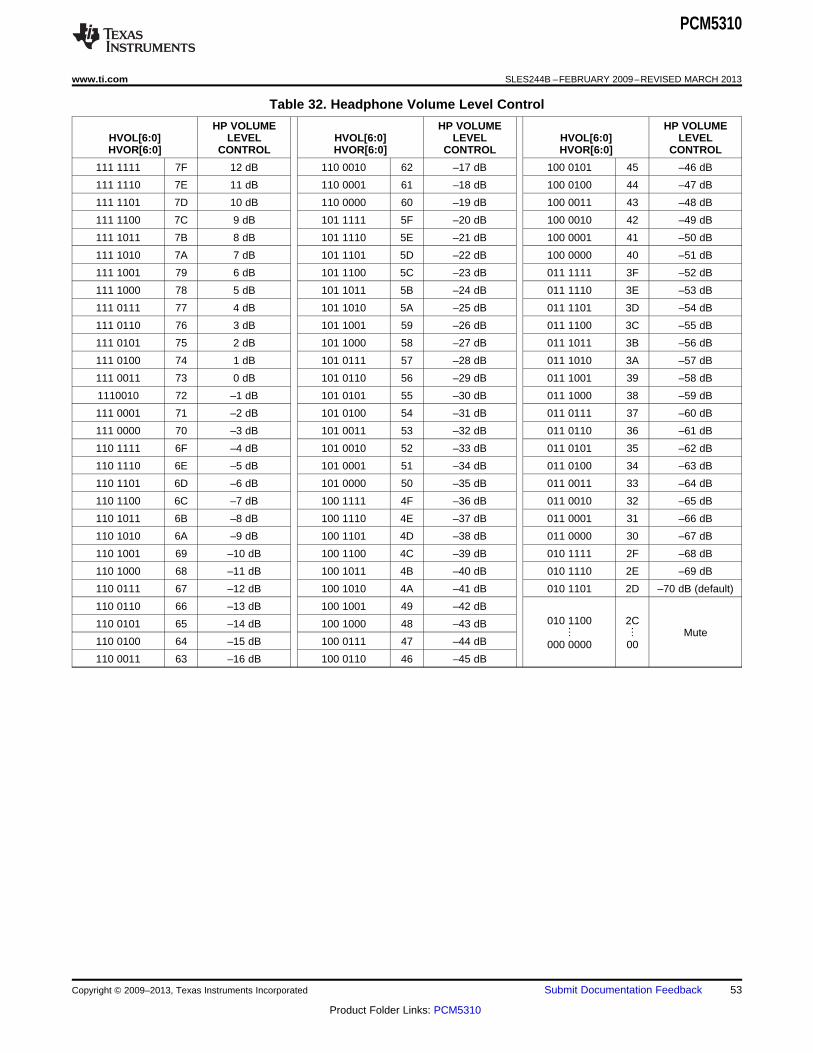
PCM5310
www.ti.com SLES244B –FEBRUARY 2009–REVISED MARCH 2013
Table 32. Headphone Volume Level Control
HP VOLUME HP VOLUME HP VOLUMEHVOL[6:0] LEVEL HVOL[6:0] LEVEL HVOL[6:0] LEVELHVOR[6:0] CONTROL HVOR[6:0] CONTROL HVOR[6:0] CONTROL
111 1111 7F 12 dB 110 0010 62 –17 dB 100 0101 45 –46 dB
111 1110 7E 11 dB 110 0001 61 –18 dB 100 0100 44 –47 dB
111 1101 7D 10 dB 110 0000 60 –19 dB 100 0011 43 –48 dB
111 1100 7C 9 dB 101 1111 5F –20 dB 100 0010 42 –49 dB
111 1011 7B 8 dB 101 1110 5E –21 dB 100 0001 41 –50 dB
111 1010 7A 7 dB 101 1101 5D –22 dB 100 0000 40 –51 dB
111 1001 79 6 dB 101 1100 5C –23 dB 011 1111 3F –52 dB
111 1000 78 5 dB 101 1011 5B –24 dB 011 1110 3E –53 dB
111 0111 77 4 dB 101 1010 5A –25 dB 011 1101 3D –54 dB
111 0110 76 3 dB 101 1001 59 –26 dB 011 1100 3C –55 dB
111 0101 75 2 dB 101 1000 58 –27 dB 011 1011 3B –56 dB
111 0100 74 1 dB 101 0111 57 –28 dB 011 1010 3A –57 dB
111 0011 73 0 dB 101 0110 56 –29 dB 011 1001 39 –58 dB
1110010 72 –1 dB 101 0101 55 –30 dB 011 1000 38 –59 dB
111 0001 71 –2 dB 101 0100 54 –31 dB 011 0111 37 –60 dB
111 0000 70 –3 dB 101 0011 53 –32 dB 011 0110 36 –61 dB
110 1111 6F –4 dB 101 0010 52 –33 dB 011 0101 35 –62 dB
110 1110 6E –5 dB 101 0001 51 –34 dB 011 0100 34 –63 dB
110 1101 6D –6 dB 101 0000 50 –35 dB 011 0011 33 –64 dB
110 1100 6C –7 dB 100 1111 4F –36 dB 011 0010 32 –65 dB
110 1011 6B –8 dB 100 1110 4E –37 dB 011 0001 31 –66 dB
110 1010 6A –9 dB 100 1101 4D –38 dB 011 0000 30 –67 dB
110 1001 69 –10 dB 100 1100 4C –39 dB 010 1111 2F –68 dB
110 1000 68 –11 dB 100 1011 4B –40 dB 010 1110 2E –69 dB
110 0111 67 –12 dB 100 1010 4A –41 dB 010 1101 2D –70 dB (default)
110 0110 66 –13 dB 100 1001 49 –42 dB010 1100 2C110 0101 65 –14 dB 100 1000 48 –43 dB
⋮ ⋮ Mute110 0100 64 –15 dB 100 0111 47 –44 dB 000 0000 00110 0011 63 –16 dB 100 0110 46 –45 dB
Copyright © 2009–2013, Texas Instruments Incorporated Submit Documentation Feedback 53
Product Folder Links: PCM5310
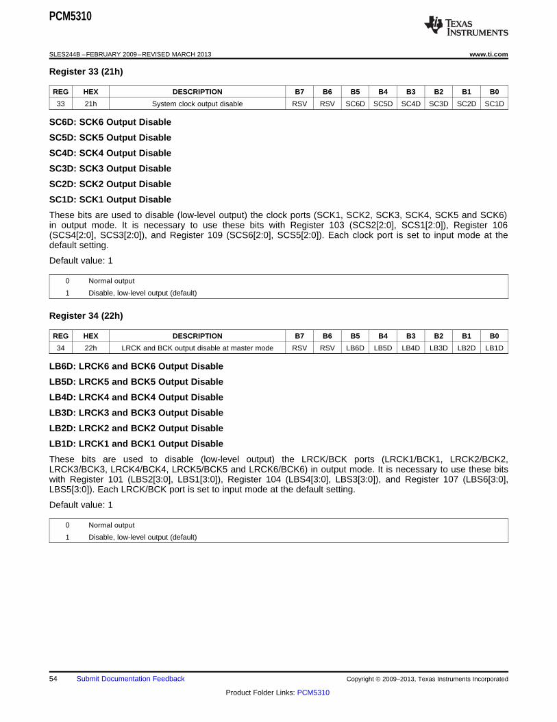
PCM5310
SLES244B –FEBRUARY 2009–REVISED MARCH 2013 www.ti.com
Register 33 (21h)
REG HEX DESCRIPTION B7 B6 B5 B4 B3 B2 B1 B0
33 21h System clock output disable RSV RSV SC6D SC5D SC4D SC3D SC2D SC1D
SC6D: SCK6 Output Disable
SC5D: SCK5 Output Disable
SC4D: SCK4 Output Disable
SC3D: SCK3 Output Disable
SC2D: SCK2 Output Disable
SC1D: SCK1 Output Disable
These bits are used to disable (low-level output) the clock ports (SCK1, SCK2, SCK3, SCK4, SCK5 and SCK6)in output mode. It is necessary to use these bits with Register 103 (SCS2[2:0], SCS1[2:0]), Register 106(SCS4[2:0], SCS3[2:0]), and Register 109 (SCS6[2:0], SCS5[2:0]). Each clock port is set to input mode at thedefault setting.
Default value: 1
0 Normal output
1 Disable, low-level output (default)
Register 34 (22h)
REG HEX DESCRIPTION B7 B6 B5 B4 B3 B2 B1 B0
34 22h LRCK and BCK output disable at master mode RSV RSV LB6D LB5D LB4D LB3D LB2D LB1D
LB6D: LRCK6 and BCK6 Output Disable
LB5D: LRCK5 and BCK5 Output Disable
LB4D: LRCK4 and BCK4 Output Disable
LB3D: LRCK3 and BCK3 Output Disable
LB2D: LRCK2 and BCK2 Output Disable
LB1D: LRCK1 and BCK1 Output Disable
These bits are used to disable (low-level output) the LRCK/BCK ports (LRCK1/BCK1, LRCK2/BCK2,LRCK3/BCK3, LRCK4/BCK4, LRCK5/BCK5 and LRCK6/BCK6) in output mode. It is necessary to use these bitswith Register 101 (LBS2[3:0], LBS1[3:0]), Register 104 (LBS4[3:0], LBS3[3:0]), and Register 107 (LBS6[3:0],LBS5[3:0]). Each LRCK/BCK port is set to input mode at the default setting.
Default value: 1
0 Normal output
1 Disable, low-level output (default)
54 Submit Documentation Feedback Copyright © 2009–2013, Texas Instruments Incorporated
Product Folder Links: PCM5310
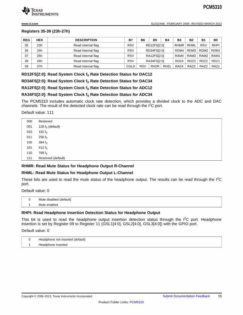
PCM5310
www.ti.com SLES244B –FEBRUARY 2009–REVISED MARCH 2013
Registers 35-39 (23h-27h)
REG HEX DESCRIPTION B7 B6 B5 B4 B3 B2 B1 B0
35 23h Read internal flag RSV RD12FS[2:0] RHMR RHML RSV RHPI
36 24h Read internal flag RSV RD34FS[2:0] RDM4 RDM3 RDM2 RDM1
37 25h Read internal flag RSV RA12FS[2:0] RAM4 RAM3 RAM2 RAM1
38 26h Read internal flag RSV RA34FS[2:0] RDZ4 RDZ3 RDZ2 RDZ1
39 27h Read internal flag CGLD RSV RHZR RHZL RAZ4 RAZ3 RAZ2 RAZ1
RD12FS[2:0]: Read System Clock fS Rate Detection Status for DAC12
RD34FS[2:0]: Read System Clock fS Rate Detection Status for DAC34
RA12FS[2:0]: Read System Clock fS Rate Detection Status for ADC12
RA34FS[2:0]: Read System Clock fS Rate Detection Status for ADC34
The PCM5310 includes automatic clock rate detection, which provides a divided clock to the ADC and DACchannels. The result of the detected clock rate can be read through the I2C port.
Default value: 111
000 Reserved
001 128 fS (default)
010 192 fS
011 256 fS
100 384 fS
101 512 fS
110 768 fS
111 Reserved (default)
RHMR: Read Mute Status for Headphone Output R-Channel
RHML: Read Mute Status for Headphone Output L-Channel
These bits are used to read the mute status of the headphone output. The results can be read through the I2Cport.
Default value: 0
0 Mute disabled (default)
1 Mute enabled
RHPI: Read Headphone Insertion Detection Status for Headphone Output
This bit is used to read the headphone output insertion detection status through the I2C port. Headphoneinsertion is set by Register 09 to Register 11 (GSL1[4:0], GSL2[4:0], GSL3[4:0]) with the GPIO port.
Default value: 0
0 Headphone not inserted (default)
1 Headphone inserted
Copyright © 2009–2013, Texas Instruments Incorporated Submit Documentation Feedback 55
Product Folder Links: PCM5310

PCM5310
SLES244B –FEBRUARY 2009–REVISED MARCH 2013 www.ti.com
RDM4: Read Digital Mute Status for DAC34, R-Channel
RDM3: Read Digital Mute Status for DAC34, L-Channel
RDM2: Read Digital Mute Status for DAC12, R-Channel
RDM1: Read Digital Mute Status for DAC12, L-Channel
These bits are used to read the digital soft mute status for each DAC channel through the I2C port.
Default value: 1
0 Mute disabled
1 Mute enabled (default)
RAM4: Read Digital Mute Status for ADC34, R-Channel
RAM3: Read Digital Mute Status for ADC34, L-Channel
RAM2: Read Digital Mute Status for ADC12, R-Channel
RAM1: Read Digital Mute Status for ADC12, L-Channel
These bits are used to read the digital soft mute status for each ADC channel through the I2C port.
Default value: 1
0 Mute disabled
1 Mute enabled (default)
RRHZR: Read Volume Zero Cross Time Out Status for Headphone, R-Channel
RHZL: Read Volume Zero Cross Time Out Status for Headphone, L-Channel
RDZ4: Read Digital Attenuation/Mute Zero Cross Timeout Status for DAC34, R-Channel
RDZ3: Read Digital Attenuation/Mute Zero Cross Timeout Status for DAC34, L-Channel
RDZ2: Read Digital Attenuation/Mute Zero Cross Timeout Status for DAC12, R-Channel
RDZ1: Read Digital Attenuation/Mute Zero Cross Timeout Status for DAC12, L-Channel
RAZ4: Read Digital Attenuation/Mute Zero Cross Timeout Status for ADC34, R-Channel
RAZ3: Read Digital Attenuation/Mute Zero Cross Timeout Status for ADC34, L-Channel
RAZ2: Read Digital Attenuation/Mute Zero Cross Timeout Status for ADC12, R-Channel
RAZ1: Read Digital Attenuation/Mute Zero Cross Timeout Status for ADC12, L-Channel
These bits are used to read the zero-crossing timeout status of digital soft mute and digital attenuation for eachADCs and DACs channel and for headphone output volume through the I2C port.
Default value: 0
0 not timed out (default)
1 Timed out
CGLD: Glitch Reduction Disable when Changing Clock Source
This bit disables the glitch reduction circuit, which reduces audible pop noise when changing the clock input fromany SCKx to SCKx.
Default value: 0
0 Enabled (default)
1 Disabled
56 Submit Documentation Feedback Copyright © 2009–2013, Texas Instruments Incorporated
Product Folder Links: PCM5310
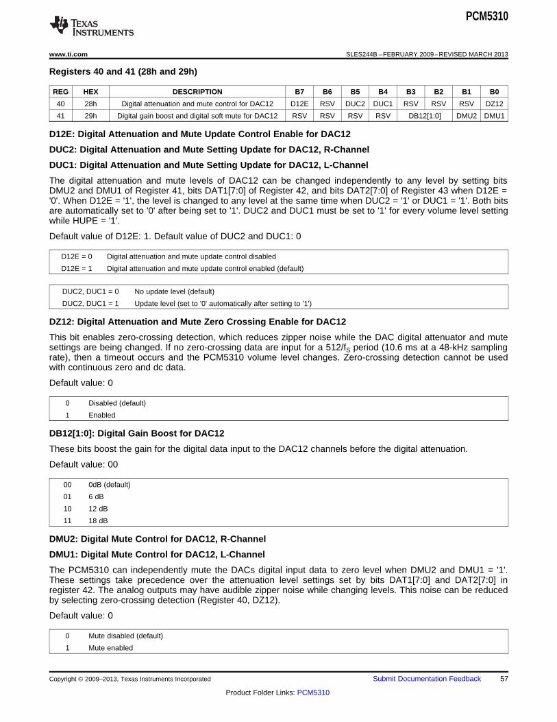
PCM5310
www.ti.com SLES244B –FEBRUARY 2009–REVISED MARCH 2013
Registers 40 and 41 (28h and 29h)
REG HEX DESCRIPTION B7 B6 B5 B4 B3 B2 B1 B0
40 28h Digital attenuation and mute control for DAC12 D12E RSV DUC2 DUC1 RSV RSV RSV DZ12
41 29h Digital gain boost and digital soft mute for DAC12 RSV RSV RSV RSV DB12[1:0] DMU2 DMU1
D12E: Digital Attenuation and Mute Update Control Enable for DAC12
DUC2: Digital Attenuation and Mute Setting Update for DAC12, R-Channel
DUC1: Digital Attenuation and Mute Setting Update for DAC12, L-Channel
The digital attenuation and mute levels of DAC12 can be changed independently to any level by setting bitsDMU2 and DMU1 of Register 41, bits DAT1[7:0] of Register 42, and bits DAT2[7:0] of Register 43 when D12E ='0'. When D12E = '1', the level is changed to any level at the same time when DUC2 = '1' or DUC1 = '1'. Both bitsare automatically set to '0' after being set to '1'. DUC2 and DUC1 must be set to '1' for every volume level settingwhile HUPE = '1'.
Default value of D12E: 1. Default value of DUC2 and DUC1: 0
D12E = 0 Digital attenuation and mute update control disabled
D12E = 1 Digital attenuation and mute update control enabled (default)
DUC2, DUC1 = 0 No update level (default)
DUC2, DUC1 = 1 Update level (set to '0' automatically after setting to '1')
DZ12: Digital Attenuation and Mute Zero Crossing Enable for DAC12
This bit enables zero-crossing detection, which reduces zipper noise while the DAC digital attenuator and mutesettings are being changed. If no zero-crossing data are input for a 512/fS period (10.6 ms at a 48-kHz samplingrate), then a timeout occurs and the PCM5310 volume level changes. Zero-crossing detection cannot be usedwith continuous zero and dc data.
Default value: 0
0 Disabled (default)
1 Enabled
DB12[1:0]: Digital Gain Boost for DAC12
These bits boost the gain for the digital data input to the DAC12 channels before the digital attenuation.
Default value: 00
00 0dB (default)
01 6 dB
10 12 dB
11 18 dB
DMU2: Digital Mute Control for DAC12, R-Channel
DMU1: Digital Mute Control for DAC12, L-Channel
The PCM5310 can independently mute the DACs digital input data to zero level when DMU2 and DMU1 = '1'.These settings take precedence over the attenuation level settings set by bits DAT1[7:0] and DAT2[7:0] inregister 42. The analog outputs may have audible zipper noise while changing levels. This noise can be reducedby selecting zero-crossing detection (Register 40, DZ12).
Default value: 0
0 Mute disabled (default)
1 Mute enabled
Copyright © 2009–2013, Texas Instruments Incorporated Submit Documentation Feedback 57
Product Folder Links: PCM5310

PCM5310
SLES244B –FEBRUARY 2009–REVISED MARCH 2013 www.ti.com
Registers 42 and 43 (2Ah and 2Bh)
REG HEX DESCRIPTION B7 B6 B5 B4 B3 B2 B1 B0
42 2Ah Digital attenuation level setting for DAC12 L-channel DAT1[7:0]
43 2Bh Digital attenuation level setting for DAC12 R-channel DAT2[7:0]
DAT1[7:0]: Digital Attenuation Setting for DAC12, L-Channel
DAT2[7:0]: Digital Attenuation Setting for DAC12, R-Channel
The digital attenuator of DAC12 can be independently set from 0 dB to –100 dB in 0.5-dB steps. The DAC12output may have audible zipper noise while changing levels. This noise can be reduced by selecting zerocrossing detection (Register 40, DZ12).
Default value : 1111 1111
Table 33. Digital Attenuation Level Setting for DAC12
DIGITAL ATT DIGITAL ATT DIGITAL ATT DIGITAL ATTDAT1[7:0] LEVEL DAT1[7:0] LEVEL DAT1[7:0] LEVEL DAT1[7:0] LEVELDAT2[7:0] SETTING DAT2[7:0] SETTING DAT2[7:0] SETTING DAT2[7:0] SETTING
1111 1111 FF 0 dB (default) 1100 1100 CC –25.5 dB 1001 1001 99 – 51 dB 0110 0110 66 –76.5 dB
1111 1110 FE –0.5 dB 1100 1011 CB –26 dB 1001 1000 98 –51.5 dB 0110 0101 65 –77 dB
1111 1101 FD –1 dB 1100 1010 CA –26.5 dB 1001 0111 97 –52 dB 0110 0100 64 –77.5 dB
1111 1100 FC –1.5 dB 1100 1001 C9 –27 dB 1001 0110 96 –52.5 dB 0110 0011 63 –78 dB
1111 1011 FB –2 dB 1100 1000 C8 –27.5 dB 1001 0101 95 –53 dB 0110 0010 62 –78.8 dB
1111 1010 FA –2.5 dB 1100 0111 C7 –28 dB 1001 0100 94 –53.5 dB 0110 0001 61 –79 dB
1111 1001 F9 –3 dB 1100 0110 C6 –28.5 dB 1001 0011 93 –54 dB 0110 0000 60 –79.5 dB
1111 1000 F8 –3.5 dB 1100 0101 C5 –29 dB 1001 0010 92 –54.5 dB 0101 1111 5F –80 dB
1111 0111 F7 –4 dB 1100 0100 C4 –29.5 dB 1001 0001 91 –55 dB 0101 1110 5E –80.5 dB
1111 0110 F6 –4.5 dB 1100 0011 C3 –30 dB 1001 0000 90 –55.5 dB 0101 1101 5D –81 dB
1111 0101 F5 –5 dB 1100 0010 C2 –30.5 dB 1000 1111 8F –56 dB 0101 1100 5C –81.5 dB
1111 0100 F4 –5.5 dB 1100 0001 C1 –31 dB 1000 1110 8E –56.5 dB 0101 1011 5B –82 dB
1111 0011 F3 –6 dB 1100 0000 C0 –31.5 dB 1000 1101 8D –57 dB 0101 1010 5A –82.5 dB
1111 0010 F2 –6.5 dB 1011 1111 BF –32 dB 1000 1100 8C –57.5 dB 0101 1001 59 –83 dB
1111 0001 F1 –7 dB 1011 1110 BE –32.5 dB 1000 1011 8B –58 dB 0101 1000 58 –83.5 dB
1111 0000 F0 –7.5 dB 1011 1101 BD –33 dB 1000 1010 8A –58.5 dB 0101 0111 57 –84 dB
1110 1111 EF –8 dB 1011 1100 BC –33.5 dB 1000 1001 89 –59 dB 0101 0110 56 –84.5 dB
1110 1110 EE –8.5 dB 1011 1011 BB –34 dB 1000 1000 88 –59.5 dB 0101 0101 55 –85 dB
1110 1101 ED –9 dB 1011 1010 BA –34.5 dB 1000 0111 87 –60 dB 0101 0100 54 –85.5 dB
1110 1100 EC –9.5 dB 1011 1001 B9 –35 dB 1000 0110 86 –60.5 dB 0101 0011 53 –86 dB
1110 1011 EB –10 dB 1011 1000 B8 –35.5 dB 1000 0101 85 –61 dB 0101 0010 52 –86.5 dB
1110 1010 EA –10.5 dB 1011 0111 B7 –36 dB 1000 0100 84 –61.5 dB 0101 0001 51 –87 dB
1110 1001 E9 –11 dB 1011 0110 B6 –36.5 dB 1000 0011 83 –62 dB 0101 0000 50 –87.5 dB
1110 1000 E8 –11.5 dB 1011 0101 B5 –37 dB 1000 0010 82 –62.5 dB 0100 1111 4F –88 dB
1110 0111 E7 –12 dB 1011 0100 B4 –37.5 dB 1000 0001 81 –63 dB 0100 1110 4E –88.5 dB
1110 0110 E6 –12.5 dB 1011 0011 B3 –38 dB 1000 0000 80 –63.5 dB 0100 1101 4D –89 dB
1110 0101 E5 –13 dB 1011 0010 B2 –38.5 dB 0111 1111 7F –64 dB 0100 1100 4C –89.5 dB
1110 0100 E4 –13.5 dB 1011 0001 B1 –39 dB 0111 1110 7E –64.5 dB 0100 1011 4B –90 dB
1110 0011 E3 –14 dB 1011 0000 B0 –39.5 dB 0111 1101 7D –65 dB 0100 1010 4A –90.5 dB
1110 0010 E2 –14.5 dB 1010 1111 AF –40 dB 0111 1100 7C –65.5 dB 0100 1001 49 –91 dB
1110 0001 E1 –15 dB 1010 1110 AE –40.5 dB 0111 1011 7B –66 dB 0100 1000 48 –91.5 dB
1110 0000 E0 –15.5 dB 1010 1101 AD –41 dB 0111 1010 7A –66.5 dB 0100 0111 47 –92 dB
1101 1111 DF –16 dB 1010 1100 AC –41.5 dB 0111 1001 79 –67 dB 0100 0110 46 –92.5 dB
1101 1110 DE –16.5 dB 1010 1011 AB –42 dB 0111 1000 78 –67.5 dB 0100 0101 45 –93 dB
58 Submit Documentation Feedback Copyright © 2009–2013, Texas Instruments Incorporated
Product Folder Links: PCM5310
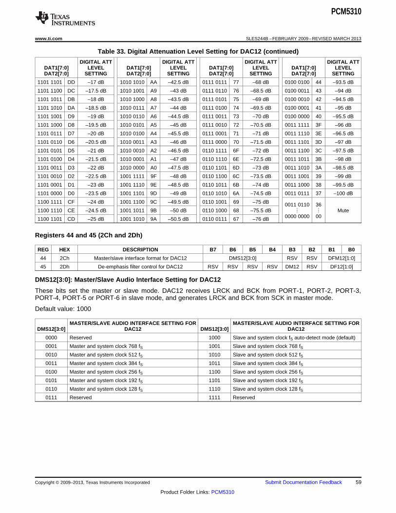
PCM5310
www.ti.com SLES244B –FEBRUARY 2009–REVISED MARCH 2013
Table 33. Digital Attenuation Level Setting for DAC12 (continued)
DIGITAL ATT DIGITAL ATT DIGITAL ATT DIGITAL ATTDAT1[7:0] LEVEL DAT1[7:0] LEVEL DAT1[7:0] LEVEL DAT1[7:0] LEVELDAT2[7:0] SETTING DAT2[7:0] SETTING DAT2[7:0] SETTING DAT2[7:0] SETTING
1101 1101 DD –17 dB 1010 1010 AA –42.5 dB 0111 0111 77 –68 dB 0100 0100 44 –93.5 dB
1101 1100 DC –17.5 dB 1010 1001 A9 –43 dB 0111 0110 76 –68.5 dB 0100 0011 43 –94 dB
1101 1011 DB –18 dB 1010 1000 A8 –43.5 dB 0111 0101 75 –69 dB 0100 0010 42 –94.5 dB
1101 1010 DA –18.5 dB 1010 0111 A7 –44 dB 0111 0100 74 –69.5 dB 0100 0001 41 –95 dB
1101 1001 D9 –19 dB 1010 0110 A6 –44.5 dB 0111 0011 73 –70 dB 0100 0000 40 –95.5 dB
1101 1000 D8 –19.5 dB 1010 0101 A5 –45 dB 0111 0010 72 –70.5 dB 0011 1111 3F –96 dB
1101 0111 D7 –20 dB 1010 0100 A4 –45.5 dB 0111 0001 71 –71 dB 0011 1110 3E –96.5 dB
1101 0110 D6 –20.5 dB 1010 0011 A3 –46 dB 0111 0000 70 –71.5 dB 0011 1101 3D –97 dB
1101 0101 D5 –21 dB 1010 0010 A2 –46.5 dB 0110 1111 6F –72 dB 0011 1100 3C –97.5 dB
1101 0100 D4 –21.5 dB 1010 0001 A1 –47 dB 0110 1110 6E –72.5 dB 0011 1011 3B –98 dB
1101 0011 D3 –22 dB 1010 0000 A0 –47.5 dB 0110 1101 6D –73 dB 0011 1010 3A –98.5 dB
1101 0010 D2 –22.5 dB 1001 1111 9F –48 dB 0110 1100 6C –73.5 dB 0011 1001 39 –99 dB
1101 0001 D1 –23 dB 1001 1110 9E –48.5 dB 0110 1011 6B –74 dB 0011 1000 38 –99.5 dB
1101 0000 D0 –23.5 dB 1001 1101 9D –49 dB 0110 1010 6A –74.5 dB 0011 0111 37 –100 dB
1100 1111 CF –24 dB 1001 1100 9C –49.5 dB 0110 1001 69 –75 dB 0011 0110 361100 1110 CE –24.5 dB 1001 1011 9B –50 dB 0110 1000 68 –75.5 dB ⋮ ⋮ Mute
0000 0000 001100 1101 CD –25 dB 1001 1010 9A –50.5 dB 0110 0111 67 –76 dB
Registers 44 and 45 (2Ch and 2Dh)
REG HEX DESCRIPTION B7 B6 B5 B4 B3 B2 B1 B0
44 2Ch Master/slave interface format for DAC12 DMS12[3:0] RSV RSV DFM12[1:0]
45 2Dh De-emphasis filter control for DAC12 RSV RSV RSV RSV DM12 RSV DF12[1:0]
DMS12[3:0]: Master/Slave Audio Interface Setting for DAC12
These bits set the master or slave mode. DAC12 receives LRCK and BCK from PORT-1, PORT-2, PORT-3,PORT-4, PORT-5 or PORT-6 in slave mode, and generates LRCK and BCK from SCK in master mode.
Default value: 1000
MASTER/SLAVE AUDIO INTERFACE SETTING FOR MASTER/SLAVE AUDIO INTERFACE SETTING FORDMS12[3:0] DAC12 DMS12[3:0] DAC12
0000 Reserved 1000 Slave and system clock fS auto-detect mode (default)
0001 Master and system clock 768 fS 1001 Slave and system clock 768 fS
0010 Master and system clock 512 fS 1010 Slave and system clock 512 fS
0011 Master and system clock 384 fS 1011 Slave and system clock 384 fS
0100 Master and system clock 256 fS 1100 Slave and system clock 256 fS
0101 Master and system clock 192 fS 1101 Slave and system clock 192 fS
0110 Master and system clock 128 fS 1110 Slave and system clock 128 fS
0111 Reserved 1111 Reserved
Copyright © 2009–2013, Texas Instruments Incorporated Submit Documentation Feedback 59
Product Folder Links: PCM5310

PCM5310
SLES244B –FEBRUARY 2009–REVISED MARCH 2013 www.ti.com
DFM12[1:0]: Audio Interface Format for DAC12
These bits select the DAC12 audio data format as I2S, right-justified, or left-justified.
Default value: 00
00 16 to 24 bits, I2S (default)
01 16 to 24 bits, left-justified
10 24 bits, right-justified
11 16 bits, right-justified
DM12: De-Emphasis Filter Enable for DAC12
This bit enables the DAC12 de-emphasis filter. The frequency can be selected by setting bits DF12[1:0] ofRegister 45.
Default value: 0
0 Disable (default)
1 Enable
DF12[1:0]: De-Emphasis Filter Sampling Rate Selection for DAC12
A digital de-emphasis filter is in front of the interpolation filter. One of three de-emphasis filters can be selectedcorresponding to the sampling rate: 32 kHz, 44.1 kHz, or 48 kHz.
Default value: 00
00 44.1 kHz (default)
01 48 kHz
10 32 kHz
11 Reserved
Register 46 (2Eh)
REG HEX DESCRIPTION B7 B6 B5 B4 B3 B2 B1 B0
46 2Eh Power up/down, oversampling rate control for DAC12 PD12 RSV OV12[1:0] ZR12 RSV RSV RSV
PD12: Power Up/Down Control for DAC12
This bit controls the power up/down for DAC12, including the interpolation filter.
Default value: 1
0 Power up
1 Power down (default)
OV12[1:0]: Oversampling Rate Control for DAC12
These bits are used to control the oversampling rate of the DAC12 delta-sigma modulator.
Default value: 01
SYSTEM CLOCK RATE
OV12 128 fS, 192 fS 256 fS, 384 fS 128 fS, 192 fS00 16 fS 32 fS 64 fS
01 (default) 32 fS 64 fS 128 fS
10 — —
11 32 fS 128 fS(1) 128 fS
(1)
(1) Less than fS = 48 kHz
60 Submit Documentation Feedback Copyright © 2009–2013, Texas Instruments Incorporated
Product Folder Links: PCM5310
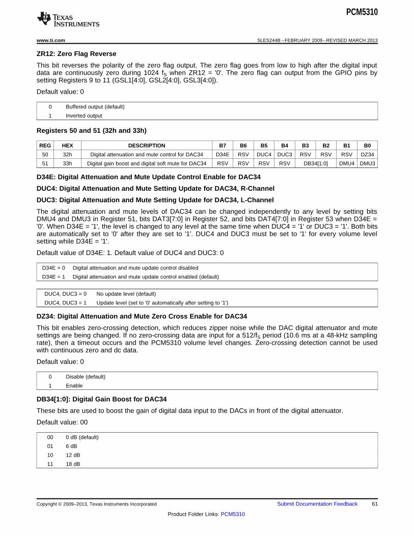
PCM5310
www.ti.com SLES244B –FEBRUARY 2009–REVISED MARCH 2013
ZR12: Zero Flag Reverse
This bit reverses the polarity of the zero flag output. The zero flag goes from low to high after the digital inputdata are continuously zero during 1024 fS when ZR12 = '0'. The zero flag can output from the GPIO pins bysetting Registers 9 to 11 (GSL1[4:0], GSL2[4:0], GSL3[4:0]).
Default value: 0
0 Buffered output (default)
1 Inverted output
Registers 50 and 51 (32h and 33h)
REG HEX DESCRIPTION B7 B6 B5 B4 B3 B2 B1 B0
50 32h Digital attenuation and mute control for DAC34 D34E RSV DUC4 DUC3 RSV RSV RSV DZ34
51 33h Digital gain boost and digital soft mute for DAC34 RSV RSV RSV RSV DB34[1:0] DMU4 DMU3
D34E: Digital Attenuation and Mute Update Control Enable for DAC34
DUC4: Digital Attenuation and Mute Setting Update for DAC34, R-Channel
DUC3: Digital Attenuation and Mute Setting Update for DAC34, L-Channel
The digital attenuation and mute levels of DAC34 can be changed independently to any level by setting bitsDMU4 and DMU3 in Register 51, bits DAT3[7:0] in Register 52, and bits DAT4[7:0] in Register 53 when D34E ='0'. When D34E = '1', the level is changed to any level at the same time when DUC4 = '1' or DUC3 = '1'. Both bitsare automatically set to '0' after they are set to '1'. DUC4 and DUC3 must be set to '1' for every volume levelsetting while D34E = '1'.
Default value of D34E: 1. Default value of DUC4 and DUC3: 0
D34E = 0 Digital attenuation and mute update control disabled
D34E = 1 Digital attenuation and mute update control enabled (default)
DUC4, DUC3 = 0 No update level (default)
DUC4, DUC3 = 1 Update level (set to '0' automatically after setting to '1')
DZ34: Digital Attenuation and Mute Zero Cross Enable for DAC34
This bit enables zero-crossing detection, which reduces zipper noise while the DAC digital attenuator and mutesettings are being changed. If no zero-crossing data are input for a 512/fS period (10.6 ms at a 48-kHz samplingrate), then a timeout occurs and the PCM5310 volume level changes. Zero-crossing detection cannot be usedwith continuous zero and dc data.
Default value: 0
0 Disable (default)
1 Enable
DB34[1:0]: Digital Gain Boost for DAC34
These bits are used to boost the gain of digital data input to the DACs in front of the digital attenuator.
Default value: 00
00 0 dB (default)
01 6 dB
10 12 dB
11 18 dB
Copyright © 2009–2013, Texas Instruments Incorporated Submit Documentation Feedback 61
Product Folder Links: PCM5310

PCM5310
SLES244B –FEBRUARY 2009–REVISED MARCH 2013 www.ti.com
DMU4: Digital Mute Control for DAC34, R-Channel
DMU3: Digital Mute Control for DAC34, L-Channel
The PCM5310 can independently mute the DAC digital input data to a zero level when DMU4 and DMU3 = '1'.These settings take precedence over the attenuation level settings of bits DAT3[7:0] and DAT4[7:0] in registers52 and 53. The analog outputs may have audible zipper noise while changing levels. This noise can be reducedby selecting zero-crossing detection (Register 50, DZ34).
Default value: 0
0 Mute disabled (default)
1 Mute enabled
Registers 52 and 53 (34h and 35h)
REG HEX DESCRIPTION B7 B6 B5 B4 B3 B2 B1 B0
52 34h Digital attenuation level setting for DAC34 L-channel DAT3[7:0]
53 35h Digital attenuation level setting for DAC34 R-channel DAT4[7:0]
DAT3[7:0]: Digital Attenuation Setting for DAC34, L-Channel
DAT4[7:0]: Digital Attenuation Setting for DAC34, R-Channel
The digital attenuator of DAC34 can be independently set from 0 dB to –100 dB in 0.5-dB steps. The DAC34output may have audible zipper noise while changing levels. This noise can be reduced by selecting zerocrossing detection (Register 50, DZ34).
Default value : 1111 1111
Table 34. Digital Attenuation Level Setting for DAC34
DIGITAL ATT DIGITAL ATT DIGITAL ATT DIGITAL ATTDAT3[7:0] LEVEL DAT3[7:0] LEVEL DAT3[7:0] LEVEL DAT3[7:0] LEVELDAT4[7:0] SETTING DAT4[7:0] SETTING DAT4[7:0] SETTING DAT4[7:0] SETTING
1111 1111 FF 0 dB (default) 1100 1100 CC –25.5 dB 1001 1001 99 – 51 dB 0110 0110 66 –76.5 dB
1111 1110 FE –0.5 dB 1100 1011 CB –26 dB 1001 1000 98 –51.5 dB 0110 0101 65 –77 dB
1111 1101 FD –1 dB 1100 1010 CA –26.5 dB 1001 0111 97 –52 dB 0110 0100 64 –77.5 dB
1111 1100 FC –1.5 dB 1100 1001 C9 –27 dB 1001 0110 96 –52.5 dB 0110 0011 63 –78 dB
1111 1011 FB –2 dB 1100 1000 C8 –27.5 dB 1001 0101 95 –53 dB 0110 0010 62 –78.8 dB
1111 1010 FA –2.5 dB 1100 0111 C7 –28 dB 1001 0100 94 –53.5 dB 0110 0001 61 –79 dB
1111 1001 F9 –3 dB 1100 0110 C6 –28.5 dB 1001 0011 93 –54 dB 0110 0000 60 –79.5 dB
1111 1000 F8 –3.5 dB 1100 0101 C5 –29 dB 1001 0010 92 –54.5 dB 0101 1111 5F –80 dB
1111 0111 F7 –4 dB 1100 0100 C4 –29.5 dB 1001 0001 91 –55 dB 0101 1110 5E –80.5 dB
1111 0110 F6 –4.5 dB 1100 0011 C3 –30 dB 1001 0000 90 –55.5 dB 0101 1101 5D –81 dB
1111 0101 F5 –5 dB 1100 0010 C2 –30.5 dB 1000 1111 8F –56 dB 0101 1100 5C –81.5 dB
1111 0100 F4 –5.5 dB 1100 0001 C1 –31 dB 1000 1110 8E –56.5 dB 0101 1011 5B –82 dB
1111 0011 F3 –6 dB 1100 0000 C0 –31.5 dB 1000 1101 8D –57 dB 0101 1010 5A –82.5 dB
1111 0010 F2 –6.5 dB 1011 1111 BF –32 dB 1000 1100 8C –57.5 dB 0101 1001 59 –83 dB
1111 0001 F1 –7 dB 1011 1110 BE –32.5 dB 1000 1011 8B –58 dB 0101 1000 58 –83.5 dB
1111 0000 F0 –7.5 dB 1011 1101 BD –33 dB 1000 1010 8A –58.5 dB 0101 0111 57 –84 dB
1110 1111 EF –8 dB 1011 1100 BC –33.5 dB 1000 1001 89 –59 dB 0101 0110 56 –84.5 dB
1110 1110 EE –8.5 dB 1011 1011 BB –34 dB 1000 1000 88 –59.5 dB 0101 0101 55 –85 dB
1110 1101 ED –9 dB 1011 1010 BA –34.5 dB 1000 0111 87 –60 dB 0101 0100 54 –85.5 dB
1110 1100 EC –9.5 dB 1011 1001 B9 –35 dB 1000 0110 86 –60.5 dB 0101 0011 53 –86 dB
1110 1011 EB –10 dB 1011 1000 B8 –35.5 dB 1000 0101 85 –61 dB 0101 0010 52 –86.5 dB
1110 1010 EA –10.5 dB 1011 0111 B7 –36 dB 1000 0100 84 –61.5 dB 0101 0001 51 –87 dB
1110 1001 E9 –11 dB 1011 0110 B6 –36.5 dB 1000 0011 83 –62 dB 0101 0000 50 –87.5 dB
62 Submit Documentation Feedback Copyright © 2009–2013, Texas Instruments Incorporated
Product Folder Links: PCM5310

PCM5310
www.ti.com SLES244B –FEBRUARY 2009–REVISED MARCH 2013
Table 34. Digital Attenuation Level Setting for DAC34 (continued)
DIGITAL ATT DIGITAL ATT DIGITAL ATT DIGITAL ATTDAT3[7:0] LEVEL DAT3[7:0] LEVEL DAT3[7:0] LEVEL DAT3[7:0] LEVELDAT4[7:0] SETTING DAT4[7:0] SETTING DAT4[7:0] SETTING DAT4[7:0] SETTING
1110 1000 E8 –11.5 dB 1011 0101 B5 –37 dB 1000 0010 82 –62.5 dB 0100 1111 4F –88 dB
1110 0111 E7 –12 dB 1011 0100 B4 –37.5 dB 1000 0001 81 –63 dB 0100 1110 4E –88.5 dB
1110 0110 E6 –12.5 dB 1011 0011 B3 –38 dB 1000 0000 80 –63.5 dB 0100 1101 4D –89 dB
1110 0101 E5 –13 dB 1011 0010 B2 –38.5 dB 0111 1111 7F –64 dB 0100 1100 4C –89.5 dB
1110 0100 E4 –13.5 dB 1011 0001 B1 –39 dB 0111 1110 7E –64.5 dB 0100 1011 4B –90 dB
1110 0011 E3 –14 dB 1011 0000 B0 –39.5 dB 0111 1101 7D –65 dB 0100 1010 4A –90.5 dB
1110 0010 E2 –14.5 dB 1010 1111 AF –40 dB 0111 1100 7C –65.5 dB 0100 1001 49 –91 dB
1110 0001 E1 –15 dB 1010 1110 AE –40.5 dB 0111 1011 7B –66 dB 0100 1000 48 –91.5 dB
1110 0000 E0 –15.5 dB 1010 1101 AD –41 dB 0111 1010 7A –66.5 dB 0100 0111 47 –92 dB
1101 1111 DF –16 dB 1010 1100 AC –41.5 dB 0111 1001 79 –67 dB 0100 0110 46 –92.5 dB
1101 1110 DE –16.5 dB 1010 1011 AB –42 dB 0111 1000 78 –67.5 dB 0100 0101 45 –93 dB
1101 1101 DD –17 dB 1010 1010 AA –42.5 dB 0111 0111 77 –68 dB 0100 0100 44 –93.5 dB
1101 1100 DC –17.5 dB 1010 1001 A9 –43 dB 0111 0110 76 –68.5 dB 0100 0011 43 –94 dB
1101 1011 DB –18 dB 1010 1000 A8 –43.5 dB 0111 0101 75 –69 dB 0100 0010 42 –94.5 dB
1101 1010 DA –18.5 dB 1010 0111 A7 –44 dB 0111 0100 74 –69.5 dB 0100 0001 41 –95 dB
1101 1001 D9 –19 dB 1010 0110 A6 –44.5 dB 0111 0011 73 –70 dB 0100 0000 40 –95.5 dB
1101 1000 D8 –19.5 dB 1010 0101 A5 –45 dB 0111 0010 72 –70.5 dB 0011 1111 3F –96 dB
1101 0111 D7 –20 dB 1010 0100 A4 –45.5 dB 0111 0001 71 –71 dB 0011 1110 3E –96.5 dB
1101 0110 D6 –20.5 dB 1010 0011 A3 –46 dB 0111 0000 70 –71.5 dB 0011 1101 3D –97 dB
1101 0101 D5 –21 dB 1010 0010 A2 –46.5 dB 0110 1111 6F –72 dB 0011 1100 3C –97.5 dB
1101 0100 D4 –21.5 dB 1010 0001 A1 –47 dB 0110 1110 6E –72.5 dB 0011 1011 3B –98 dB
1101 0011 D3 –22 dB 1010 0000 A0 –47.5 dB 0110 1101 6D –73 dB 0011 1010 3A –98.5 dB
1101 0010 D2 –22.5 dB 1001 1111 9F –48 dB 0110 1100 6C –73.5 dB 0011 1001 39 –99 dB
1101 0001 D1 –23 dB 1001 1110 9E –48.5 dB 0110 1011 6B –74 dB 0011 1000 38 –99.5 dB
1101 0000 D0 –23.5 dB 1001 1101 9D –49 dB 0110 1010 6A –74.5 dB 0011 0111 37 –100 dB
1100 1111 CF –24 dB 1001 1100 9C –49.5 dB 0110 1001 69 –75 dB 0011 0110 361100 1110 CE –24.5 dB 1001 1011 9B –50 dB 0110 1000 68 –75.5 dB ⋮ ⋮ Mute
0000 0000 001100 1101 CD –25 dB 1001 1010 9A –50.5 dB 0110 0111 67 –76 dB
Copyright © 2009–2013, Texas Instruments Incorporated Submit Documentation Feedback 63
Product Folder Links: PCM5310

PCM5310
SLES244B –FEBRUARY 2009–REVISED MARCH 2013 www.ti.com
Registers 54 and 55 (36h and 37h)
REG HEX DESCRIPTION B7 B6 B5 B4 B3 B2 B1 B0
54 36h Master/slave interface format for DAC34 DMS34[3:0] RSV RSV DFM34[1:0]
55 37h De-emphasis filter control for DAC34 RSV RSV RSV RSV DM34 RSV DF34[1:0]
DMS34[3:0]: Master/Slave Audio Interface Setting for DAC34
These bits set the master or slave mode. DAC34 receives LRCK and BCK from PORT-1, PORT-2, PORT-3,PORT-4, PORT-5 or PORT-6 in slave mode, and generates LRCK and BCK from SCK in master mode.
Default value: 1000
MASTER/SLAVE AUDIO INTERFACE SETTING FOR MASTER/SLAVE AUDIO INTERFACE SETTING FORDMS34[3:0] DAC34 DMS34[3:0] DAC34
0000 Reserved 1000 Slave and system clock fS auto-detect mode (default)
0001 Master and system clock 768 fS 1001 Slave and system clock 768 fS
0010 Master and system clock 512 fS 1010 Slave and system clock 512 fS
0011 Master and system clock 384 fS 1011 Slave and system clock 384 fS
0100 Master and system clock 256 fS 1100 Slave and system clock 256 fS
0101 Master and system clock 192 fS 1101 Slave and system clock 192 fS
0110 Master and system clock 128 fS 1110 Slave and system clock 128 fS
0111 Reserved 1111 Reserved
DFM34[1:0]: Audio Interface Format for DAC34
These bits select the DAC34 audio data format as I2S, right-justified, or left-justified.
Default value: 00
00 16 to 24 bits, I2S (default)
01 16 to 24 bits, left-justified
10 24 bits, right-justified
11 16 bits, right-justified
DM34: De-Emphasis Filter Enable for DAC34
This bit enables the DAC34 de-emphasis filter. The frequency can be selected by setting bits DF34[1:0] ofRegister 55.
Default value: 0
0 Disable (default)
1 Enable
DF34[1:0]: De-Emphasis Filter Sampling Rate Selection for DAC34
A digital de-emphasis filter is in front of the interpolation filter. One of three de-emphasis filters can be selectedcorresponding to the sampling rate: 32 kHz, 44.1 kHz, or 48 kHz.
Default value: 00
00 44.1 kHz (default)
01 48 kHz
10 32 kHz
11 Reserved
64 Submit Documentation Feedback Copyright © 2009–2013, Texas Instruments Incorporated
Product Folder Links: PCM5310

PCM5310
www.ti.com SLES244B –FEBRUARY 2009–REVISED MARCH 2013
Register 56 (38h)
REG HEX DESCRIPTION B7 B6 B5 B4 B3 B2 B1 B0
56 38h Power up/down, oversampling rate control for DAC34 PD34 RSV OV34[1:0] ZR34 RSV RSV RSV
PD34: Power Up/Down Control for DAC34
This bit controls the power up/down for DAC34, including the interpolation filter.
Default value: 1
0 Power up
1 Power down (default)
OV34[1:0]: Oversampling Rate Control for DAC34
These bits control the oversampling rate of the DAC34 delta-sigma modulator.
Default value: 01
SYSTEM CLOCK RATE
OV34 128 fS, 192 fS 256 fS, 384 fS 128 fS, 192 fS00 16 fS 32 fS 64 fS
01 (default) 32 fS 64 fS 128 fS
10 — —
11 32 fS 128 fS(1) 128 fS
(1)
(1) Less than fS = 48 kHz
ZR34: Zero Flag Reverse
This bit reverses the polarity of the zero flag output. The zero flag is high after input data are zero during 1024 fSwhen ZR34 = '0', and is set with the GPIO port by bits GSL1[4:0], GSL2[4:0], GSL3[4:0] in registers 09 to 11.
Default value: 0
0 Buffered output (default)
1 Inverted output
Copyright © 2009–2013, Texas Instruments Incorporated Submit Documentation Feedback 65
Product Folder Links: PCM5310
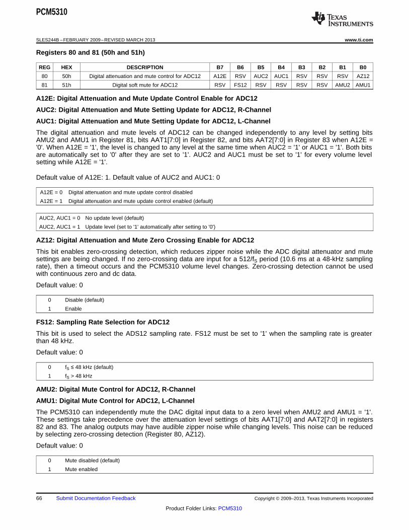
PCM5310
SLES244B –FEBRUARY 2009–REVISED MARCH 2013 www.ti.com
Registers 80 and 81 (50h and 51h)
REG HEX DESCRIPTION B7 B6 B5 B4 B3 B2 B1 B0
80 50h Digital attenuation and mute control for ADC12 A12E RSV AUC2 AUC1 RSV RSV RSV AZ12
81 51h Digital soft mute for ADC12 RSV FS12 RSV RSV RSV RSV AMU2 AMU1
A12E: Digital Attenuation and Mute Update Control Enable for ADC12
AUC2: Digital Attenuation and Mute Setting Update for ADC12, R-Channel
AUC1: Digital Attenuation and Mute Setting Update for ADC12, L-Channel
The digital attenuation and mute levels of ADC12 can be changed independently to any level by setting bitsAMU2 and AMU1 in Register 81, bits AAT1[7:0] in Register 82, and bits AAT2[7:0] in Register 83 when A12E ='0'. When A12E = '1', the level is changed to any level at the same time when AUC2 = '1' or AUC1 = '1'. Both bitsare automatically set to '0' after they are set to '1'. AUC2 and AUC1 must be set to '1' for every volume levelsetting while A12E = '1'.
Default value of A12E: 1. Default value of AUC2 and AUC1: 0
A12E = 0 Digital attenuation and mute update control disabled
A12E = 1 Digital attenuation and mute update control enabled (default)
AUC2, AUC1 = 0 No update level (default)
AUC2, AUC1 = 1 Update level (set to '1' automatically after setting to '0')
AZ12: Digital Attenuation and Mute Zero Crossing Enable for ADC12
This bit enables zero-crossing detection, which reduces zipper noise while the ADC digital attenuator and mutesettings are being changed. If no zero-crossing data are input for a 512/fS period (10.6 ms at a 48-kHz samplingrate), then a timeout occurs and the PCM5310 volume level changes. Zero-crossing detection cannot be usedwith continuous zero and dc data.
Default value: 0
0 Disable (default)
1 Enable
FS12: Sampling Rate Selection for ADC12
This bit is used to select the ADS12 sampling rate. FS12 must be set to '1' when the sampling rate is greaterthan 48 kHz.
Default value: 0
0 fS ≤ 48 kHz (default)
1 fS > 48 kHz
AMU2: Digital Mute Control for ADC12, R-Channel
AMU1: Digital Mute Control for ADC12, L-Channel
The PCM5310 can independently mute the DAC digital input data to a zero level when AMU2 and AMU1 = '1'.These settings take precedence over the attenuation level settings of bits AAT1[7:0] and AAT2[7:0] in registers82 and 83. The analog outputs may have audible zipper noise while changing levels. This noise can be reducedby selecting zero-crossing detection (Register 80, AZ12).
Default value: 0
0 Mute disabled (default)
1 Mute enabled
66 Submit Documentation Feedback Copyright © 2009–2013, Texas Instruments Incorporated
Product Folder Links: PCM5310

PCM5310
www.ti.com SLES244B –FEBRUARY 2009–REVISED MARCH 2013
Registers 82 and 83 (52h and 53h)
REG HEX DESCRIPTION B7 B6 B5 B4 B3 B2 B1 B0
82 52h Digital attenuation level setting for ADC12 L-channel AAT1[7:0]
83 53h Digital attenuation level setting for ADC12 R-channel AAT2[7:0]
AAT1[7:0]: Digital Attenuation Setting for ADC12, L-Channel
AAT2[7:0]: Digital Attenuation Setting for ADC12, R-Channel
The digital attenuator of ADC12 can be independently set from 20 dB to –100 dB in 0.5-dB steps. The ADC12output may have audible zipper noise while changing levels. This noise can be reduced by selecting zerocrossing detection (Register 80, AZ12).
Default value : 1101 0111
Table 35. Digital Attenuation Level Setting for ADC12
DIGITAL ATT DIGITAL ATT DIGITAL ATT DIGITAL ATTAAT1[7:0] LEVEL AAT1[7:0] LEVEL AAT1[7:0] LEVEL AAT1[7:0] LEVELAAT2[7:0] SETTING AAT2[7:0] SETTING AAT2[7:0] SETTING AAT2[7:0] SETTING
1111 1111 FF 20 dB 1100 0010 C2 –10.5 dB 1000 0101 85 –41 dB 0100 1000 48 –71.5 dB
1111 1110 FE 19.5 dB 1100 0001 C1 –11 dB 1000 0100 84 –41.5 dB 0100 0111 47 –72 dB
1111 1101 FD 19 dB 1100 0000 C0 –11.5 dB 1000 0011 83 –42 dB 0100 0110 46 –72.5 dB
1111 1100 FC 18.5 dB 1011 1111 BF –12 dB 1000 0010 82 –42.5 dB 0100 0101 45 –73 dB
1111 1011 FB 18 dB 1011 1110 BE –12.5 dB 1000 0001 81 –43 dB 0100 0100 44 –73.5 dB
1111 1010 FA 17.5 dB 1011 1101 BD –13 dB 1000 0000 80 –43.5 dB 0100 0011 43 –74 dB
1111 1001 F9 17 dB 1011 1100 BC –13.5 dB 0111 1111 7F –44 dB 0100 0010 42 –74.5 dB
1111 1000 F8 16.5 dB 1011 1011 BB –14 dB 0111 1110 7E –44.5 dB 0100 0001 41 –75 dB
1111 0111 F7 16 dB 1011 1010 BA –14.5 dB 0111 1101 7D –45 dB 0100 0000 40 –75.5 dB
1111 0110 F6 15.5 dB 1011 1001 B9 –15 dB 0111 1100 7C –45.5 dB 0011 1111 3F –76 dB
1111 0101 F5 15 dB 1011 1000 B8 –15.5 dB 0111 1011 7B –46 dB 0011 1110 3E –76.5 dB
1111 0100 F4 14.5 dB 1011 0111 B7 –16 dB 0111 1010 7A –46.5 dB 0011 1101 3D –77 dB
1111 0011 F3 14 dB 1011 0110 B6 –16.5 dB 0111 1001 79 –47 dB 0011 1100 3C –77.5 dB
1111 0010 F2 13.5 dB 1011 0101 B5 –17 dB 0111 1000 78 –47.5 dB 0011 1011 3B –78 dB
1111 0001 F1 13 dB 1011 0100 B4 –17.5 dB 0111 0111 77 –48 dB 0011 1010 3A –78.8 dB
1111 0000 F0 12.5 dB 1011 0011 B3 –18 dB 0111 0110 76 –48.5 dB 0011 1001 39 –79 dB
1110 1111 EF 12 dB 1011 0010 B2 –18.5 dB 0111 0101 75 –49 dB 0011 1000 38 –79.5 dB
1110 1110 EE 11.5 dB 1011 0001 B1 –19 dB 0111 0100 74 –49.5 dB 0011 0111 37 –80 dB
1110 1101 ED 11 dB 1011 0000 B0 –19.5 dB 0111 0011 73 –50 dB 0011 0110 36 –80.5 dB
1110 1100 EC 10.5 dB 1010 1111 AF –20 dB 0111 0010 72 –50.5 dB 0011 0101 35 –81 dB
1110 1011 EB 10 dB 1010 1110 AE –20.5 dB 0111 0001 71 – 51 dB 0011 0100 34 –81.5 dB
1110 1010 EA 9.5 dB 1010 1101 AD –21 dB 0111 0000 70 –51.5 dB 0011 0011 33 –82 dB
1110 1001 E9 9 dB 1010 1100 AC –21.5 dB 0110 1111 6F –52 dB 0011 0010 32 –82.5 dB
1110 1000 E8 8.5 dB 1010 1011 AB –22 dB 0110 1110 6E –52.5 dB 0011 0001 31 –83 dB
1110 0111 E7 8 dB 1010 1010 AA –22.5 dB 0110 1101 6D –53 dB 0011 0000 30 –83.5 dB
1110 0110 E6 7.5 dB 1010 1001 A9 –23 dB 0110 1100 6C –53.5 dB 0010 1111 2F –84 dB
1110 0101 E5 7 dB 1010 1000 A8 –23.5 dB 0110 1011 6B –54 dB 0010 1110 2E –84.5 dB
1110 0100 E4 6.5 dB 1010 0111 A7 –24 dB 0110 1010 6A –54.5 dB 0010 1101 2D –85 dB
1110 0011 E3 6 dB 1010 0110 A6 –24.5 dB 0110 1001 69 –55 dB 0010 1100 2C –85.5 dB
1110 0010 E2 5.5 dB 1010 0101 A5 –25 dB 0110 1000 68 –55.5 dB 0010 1011 2B –86 dB
1110 0001 E1 5 dB 1010 0100 A4 –25.5 dB 0110 0111 67 –56 dB 0010 1010 2A –86.5 dB
1110 0000 E0 4.5 dB 1010 0011 A3 –26 dB 0110 0110 66 –56.5 dB 0010 1001 29 –87 dB
1101 1111 DF 4 dB 1010 0010 A2 –26.5 dB 0110 0101 65 –57 dB 0010 1000 28 –87.5 dB
1101 1110 DE 3.5 dB 1010 0001 A1 –27 dB 0110 0100 64 –57.5 dB 0010 0111 27 –88 dB
Copyright © 2009–2013, Texas Instruments Incorporated Submit Documentation Feedback 67
Product Folder Links: PCM5310
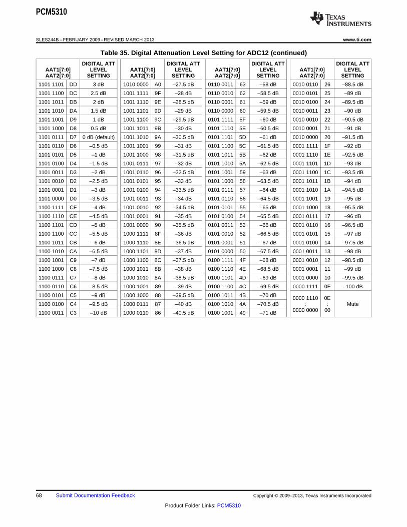
PCM5310
SLES244B –FEBRUARY 2009–REVISED MARCH 2013 www.ti.com
Table 35. Digital Attenuation Level Setting for ADC12 (continued)
DIGITAL ATT DIGITAL ATT DIGITAL ATT DIGITAL ATTAAT1[7:0] LEVEL AAT1[7:0] LEVEL AAT1[7:0] LEVEL AAT1[7:0] LEVELAAT2[7:0] SETTING AAT2[7:0] SETTING AAT2[7:0] SETTING AAT2[7:0] SETTING
1101 1101 DD 3 dB 1010 0000 A0 –27.5 dB 0110 0011 63 –58 dB 0010 0110 26 –88.5 dB
1101 1100 DC 2.5 dB 1001 1111 9F –28 dB 0110 0010 62 –58.5 dB 0010 0101 25 –89 dB
1101 1011 DB 2 dB 1001 1110 9E –28.5 dB 0110 0001 61 –59 dB 0010 0100 24 –89.5 dB
1101 1010 DA 1.5 dB 1001 1101 9D –29 dB 0110 0000 60 –59.5 dB 0010 0011 23 –90 dB
1101 1001 D9 1 dB 1001 1100 9C –29.5 dB 0101 1111 5F –60 dB 0010 0010 22 –90.5 dB
1101 1000 D8 0.5 dB 1001 1011 9B –30 dB 0101 1110 5E –60.5 dB 0010 0001 21 –91 dB
1101 0111 D7 0 dB (default) 1001 1010 9A –30.5 dB 0101 1101 5D –61 dB 0010 0000 20 –91.5 dB
1101 0110 D6 –0.5 dB 1001 1001 99 –31 dB 0101 1100 5C –61.5 dB 0001 1111 1F –92 dB
1101 0101 D5 –1 dB 1001 1000 98 –31.5 dB 0101 1011 5B –62 dB 0001 1110 1E –92.5 dB
1101 0100 D4 –1.5 dB 1001 0111 97 –32 dB 0101 1010 5A –62.5 dB 0001 1101 1D –93 dB
1101 0011 D3 –2 dB 1001 0110 96 –32.5 dB 0101 1001 59 –63 dB 0001 1100 1C –93.5 dB
1101 0010 D2 –2.5 dB 1001 0101 95 –33 dB 0101 1000 58 –63.5 dB 0001 1011 1B –94 dB
1101 0001 D1 –3 dB 1001 0100 94 –33.5 dB 0101 0111 57 –64 dB 0001 1010 1A –94.5 dB
1101 0000 D0 –3.5 dB 1001 0011 93 –34 dB 0101 0110 56 –64.5 dB 0001 1001 19 –95 dB
1100 1111 CF –4 dB 1001 0010 92 –34.5 dB 0101 0101 55 –65 dB 0001 1000 18 –95.5 dB
1100 1110 CE –4.5 dB 1001 0001 91 –35 dB 0101 0100 54 –65.5 dB 0001 0111 17 –96 dB
1100 1101 CD –5 dB 1001 0000 90 –35.5 dB 0101 0011 53 –66 dB 0001 0110 16 –96.5 dB
1100 1100 CC –5.5 dB 1000 1111 8F –36 dB 0101 0010 52 –66.5 dB 0001 0101 15 –97 dB
1100 1011 CB –6 dB 1000 1110 8E –36.5 dB 0101 0001 51 –67 dB 0001 0100 14 –97.5 dB
1100 1010 CA –6.5 dB 1000 1101 8D –37 dB 0101 0000 50 –67.5 dB 0001 0011 13 –98 dB
1100 1001 C9 –7 dB 1000 1100 8C –37.5 dB 0100 1111 4F –68 dB 0001 0010 12 –98.5 dB
1100 1000 C8 –7.5 dB 1000 1011 8B –38 dB 0100 1110 4E –68.5 dB 0001 0001 11 –99 dB
1100 0111 C7 –8 dB 1000 1010 8A –38.5 dB 0100 1101 4D –69 dB 0001 0000 10 –99.5 dB
1100 0110 C6 –8.5 dB 1000 1001 89 –39 dB 0100 1100 4C –69.5 dB 0000 1111 0F –100 dB
1100 0101 C5 –9 dB 1000 1000 88 –39.5 dB 0100 1011 4B –70 dB 0000 1110 0E1100 0100 C4 –9.5 dB 1000 0111 87 –40 dB 0100 1010 4A –70.5 dB ⋮ ⋮ Mute
0000 0000 001100 0011 C3 –10 dB 1000 0110 86 –40.5 dB 0100 1001 49 –71 dB
68 Submit Documentation Feedback Copyright © 2009–2013, Texas Instruments Incorporated
Product Folder Links: PCM5310

PCM5310
www.ti.com SLES244B –FEBRUARY 2009–REVISED MARCH 2013
Register 84 (54h)
REG HEX DESCRIPTION B7 B6 B5 B4 B3 B2 B1 B0
84 54h Master/slave interface format for ADC12 AMS12[3:0] HF12 RSV AFM12[1:0]
AMS12[3:0]: Master/Slave Audio Interface Setting for ADC12
These bits set the master or slave mode. ADC12 receives LRCK and BCK from PORT-1, PORT-2, PORT-3,PORT-4, PORT-5 or PORT-6 in slave mode, and generates LRCK and BCK from SCK in master mode.
Default value: 1000
MASTER/SLAVE AUDIO INTERFACE SETTING FOR MASTER/SLAVE AUDIO INTERFACE SETTING FORAMS12[3:0] ADC12 AMS12[3:0] ADC12
0000 Reserved 1000 Slave and system clock fS auto-detect mode (default)
0001 Master and system clock 768 fS 1001 Slave and system clock 768 fS
0010 Master and system clock 512 fS 1010 Slave and system clock 512 fS
0011 Master and system clock 384 fS 1011 Slave and system clock 384 fS
0100 Master and system clock 256 fS 1100 Slave and system clock 256 fS
0101 Reserved 1101 Reserved
0110 Reserved 1110 Reserved
0111 Reserved 1111 Reserved
HF12: High-Pass Filter Disable for ADC12
This bit disables the digital high-pass filter of ADC12.
Default value: 0
0 (0.019 fS/1000) Hz (default)
1 Off
AFM12[1:0]: Audio Interface Format for ADC12
These bits select the ADC12 audio data format as I2S, right-justified, or left-justified.
Default value: 00
00 16 to 24 bits, I2S (default)
01 16 to 24 bits, left-justified
10 24 bits, right-justified
11 16 bits, right-justified
Copyright © 2009–2013, Texas Instruments Incorporated Submit Documentation Feedback 69
Product Folder Links: PCM5310

PCM5310
SLES244B –FEBRUARY 2009–REVISED MARCH 2013 www.ti.com
Register 85 (55h)
REG HEX DESCRIPTION B7 B6 B5 B4 B3 B2 B1 B0
85 55h Power up/down for ADC12 PA12 RSV RSV RSV RSV RSV RSV RSV
PA12: Power Up/Down Control for ADC12
This bit controls the power up/down for ADC12, including the decimation filter.
Default value: 1
0 Power up
1 Power down (default)
Register 90 (5Ah)
REG HEX DESCRIPTION B7 B6 B5 B4 B3 B2 B1 B0
90 5Ah Digital attenuation and mute control for ADC34 A34E RSV AUC4 AUC3 RSV RSV RSV AZ34
A34E: Digital Attenuation and Mute Update Control Enable for ADC34
AUC4: Digital Attenuation and Mute Setting Update for ADC34, R-Channel
AUC3: Digital Attenuation and Mute Setting Update for ADC34, L-Channel
The digital attenuation and mute levels of ADC12 can be changed independently to any level by setting bitsAMU4 and AMU3 in Register 91, bits AAT3[7:0] in Register 92, and bits AAT4[7:0] in Register 93 whenA34E = '0'. When A34E = '1', the level is changed to any level at the same time when AUC4 = '1' or AUC3 = '1'.Both bits are automatically set to '0' after they are to '1'. AUC4 and AUC3 must be set to '1' for every volumelevel setting while A34E = '1'.
Default value of A34E: 1. Default value of AUC4 and AUC3: 0
A34E = 0 Digital attenuation and mute update control disabled
A34E = 1 Digital attenuation and mute update control enabled (default)
AUC4, AUC3 = 0 No update level (default)
AUC4, AUC3 = 1 Update level (set to '0' automatically after setting to '1')
AZ34: Digital Attenuation and Mute Zero Cross Enable for ADC34
This bit enables zero-crossing detection, which reduces zipper noise while the ADC digital attenuator and mutesettings are being changed. If no zero-crossing data are input for a 512/fS period (10.6 ms at a 48-kHz samplingrate), then a timeout occurs and the PCM5310 volume level changes. Zero-crossing detection cannot be usedwith continuous zero and dc data.
Default value: 0
0 Disable (default)
1 Enable
70 Submit Documentation Feedback Copyright © 2009–2013, Texas Instruments Incorporated
Product Folder Links: PCM5310
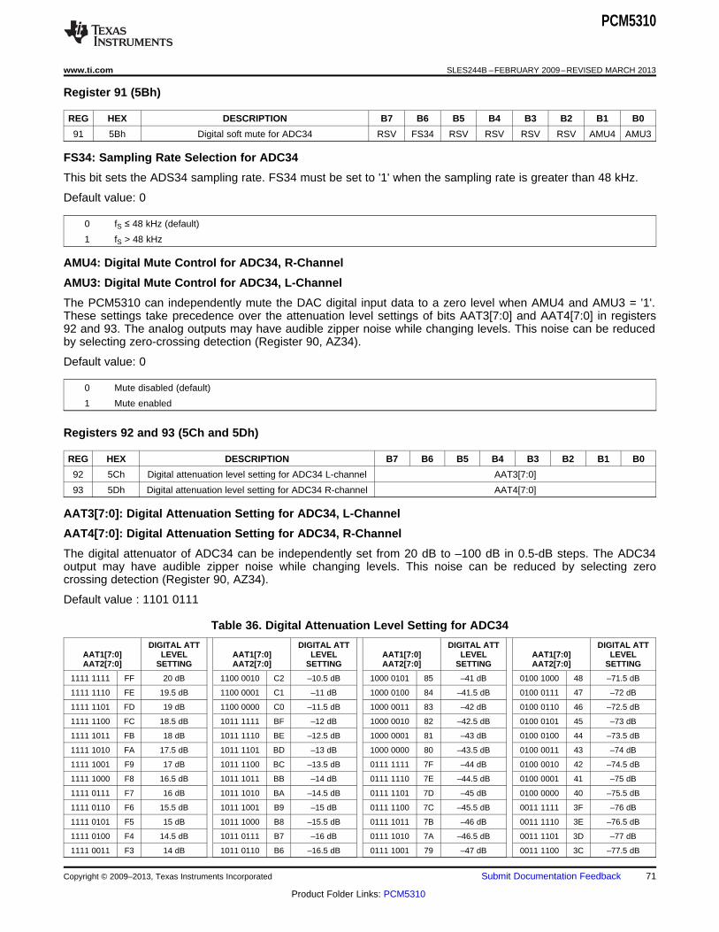
PCM5310
www.ti.com SLES244B –FEBRUARY 2009–REVISED MARCH 2013
Register 91 (5Bh)
REG HEX DESCRIPTION B7 B6 B5 B4 B3 B2 B1 B0
91 5Bh Digital soft mute for ADC34 RSV FS34 RSV RSV RSV RSV AMU4 AMU3
FS34: Sampling Rate Selection for ADC34
This bit sets the ADS34 sampling rate. FS34 must be set to '1' when the sampling rate is greater than 48 kHz.
Default value: 0
0 fS ≤ 48 kHz (default)
1 fS > 48 kHz
AMU4: Digital Mute Control for ADC34, R-Channel
AMU3: Digital Mute Control for ADC34, L-Channel
The PCM5310 can independently mute the DAC digital input data to a zero level when AMU4 and AMU3 = '1'.These settings take precedence over the attenuation level settings of bits AAT3[7:0] and AAT4[7:0] in registers92 and 93. The analog outputs may have audible zipper noise while changing levels. This noise can be reducedby selecting zero-crossing detection (Register 90, AZ34).
Default value: 0
0 Mute disabled (default)
1 Mute enabled
Registers 92 and 93 (5Ch and 5Dh)
REG HEX DESCRIPTION B7 B6 B5 B4 B3 B2 B1 B0
92 5Ch Digital attenuation level setting for ADC34 L-channel AAT3[7:0]
93 5Dh Digital attenuation level setting for ADC34 R-channel AAT4[7:0]
AAT3[7:0]: Digital Attenuation Setting for ADC34, L-Channel
AAT4[7:0]: Digital Attenuation Setting for ADC34, R-Channel
The digital attenuator of ADC34 can be independently set from 20 dB to –100 dB in 0.5-dB steps. The ADC34output may have audible zipper noise while changing levels. This noise can be reduced by selecting zerocrossing detection (Register 90, AZ34).
Default value : 1101 0111
Table 36. Digital Attenuation Level Setting for ADC34
DIGITAL ATT DIGITAL ATT DIGITAL ATT DIGITAL ATTAAT1[7:0] LEVEL AAT1[7:0] LEVEL AAT1[7:0] LEVEL AAT1[7:0] LEVELAAT2[7:0] SETTING AAT2[7:0] SETTING AAT2[7:0] SETTING AAT2[7:0] SETTING
1111 1111 FF 20 dB 1100 0010 C2 –10.5 dB 1000 0101 85 –41 dB 0100 1000 48 –71.5 dB
1111 1110 FE 19.5 dB 1100 0001 C1 –11 dB 1000 0100 84 –41.5 dB 0100 0111 47 –72 dB
1111 1101 FD 19 dB 1100 0000 C0 –11.5 dB 1000 0011 83 –42 dB 0100 0110 46 –72.5 dB
1111 1100 FC 18.5 dB 1011 1111 BF –12 dB 1000 0010 82 –42.5 dB 0100 0101 45 –73 dB
1111 1011 FB 18 dB 1011 1110 BE –12.5 dB 1000 0001 81 –43 dB 0100 0100 44 –73.5 dB
1111 1010 FA 17.5 dB 1011 1101 BD –13 dB 1000 0000 80 –43.5 dB 0100 0011 43 –74 dB
1111 1001 F9 17 dB 1011 1100 BC –13.5 dB 0111 1111 7F –44 dB 0100 0010 42 –74.5 dB
1111 1000 F8 16.5 dB 1011 1011 BB –14 dB 0111 1110 7E –44.5 dB 0100 0001 41 –75 dB
1111 0111 F7 16 dB 1011 1010 BA –14.5 dB 0111 1101 7D –45 dB 0100 0000 40 –75.5 dB
1111 0110 F6 15.5 dB 1011 1001 B9 –15 dB 0111 1100 7C –45.5 dB 0011 1111 3F –76 dB
1111 0101 F5 15 dB 1011 1000 B8 –15.5 dB 0111 1011 7B –46 dB 0011 1110 3E –76.5 dB
1111 0100 F4 14.5 dB 1011 0111 B7 –16 dB 0111 1010 7A –46.5 dB 0011 1101 3D –77 dB
1111 0011 F3 14 dB 1011 0110 B6 –16.5 dB 0111 1001 79 –47 dB 0011 1100 3C –77.5 dB
Copyright © 2009–2013, Texas Instruments Incorporated Submit Documentation Feedback 71
Product Folder Links: PCM5310

PCM5310
SLES244B –FEBRUARY 2009–REVISED MARCH 2013 www.ti.com
Table 36. Digital Attenuation Level Setting for ADC34 (continued)DIGITAL ATT DIGITAL ATT DIGITAL ATT DIGITAL ATT
AAT1[7:0] LEVEL AAT1[7:0] LEVEL AAT1[7:0] LEVEL AAT1[7:0] LEVELAAT2[7:0] SETTING AAT2[7:0] SETTING AAT2[7:0] SETTING AAT2[7:0] SETTING
1111 0010 F2 13.5 dB 1011 0101 B5 –17 dB 0111 1000 78 –47.5 dB 0011 1011 3B –78 dB
1111 0001 F1 13 dB 1011 0100 B4 –17.5 dB 0111 0111 77 –48 dB 0011 1010 3A –78.8 dB
1111 0000 F0 12.5 dB 1011 0011 B3 –18 dB 0111 0110 76 –48.5 dB 0011 1001 39 –79 dB
1110 1111 EF 12 dB 1011 0010 B2 –18.5 dB 0111 0101 75 –49 dB 0011 1000 38 –79.5 dB
1110 1110 EE 11.5 dB 1011 0001 B1 –19 dB 0111 0100 74 –49.5 dB 0011 0111 37 –80 dB
1110 1101 ED 11 dB 1011 0000 B0 –19.5 dB 0111 0011 73 –50 dB 0011 0110 36 –80.5 dB
1110 1100 EC 10.5 dB 1010 1111 AF –20 dB 0111 0010 72 –50.5 dB 0011 0101 35 –81 dB
1110 1011 EB 10 dB 1010 1110 AE –20.5 dB 0111 0001 71 – 51 dB 0011 0100 34 –81.5 dB
1110 1010 EA 9.5 dB 1010 1101 AD –21 dB 0111 0000 70 –51.5 dB 0011 0011 33 –82 dB
1110 1001 E9 9 dB 1010 1100 AC –21.5 dB 0110 1111 6F –52 dB 0011 0010 32 –82.5 dB
1110 1000 E8 8.5 dB 1010 1011 AB –22 dB 0110 1110 6E –52.5 dB 0011 0001 31 –83 dB
1110 0111 E7 8 dB 1010 1010 AA –22.5 dB 0110 1101 6D –53 dB 0011 0000 30 –83.5 dB
1110 0110 E6 7.5 dB 1010 1001 A9 –23 dB 0110 1100 6C –53.5 dB 0010 1111 2F –84 dB
1110 0101 E5 7 dB 1010 1000 A8 –23.5 dB 0110 1011 6B –54 dB 0010 1110 2E –84.5 dB
1110 0100 E4 6.5 dB 1010 0111 A7 –24 dB 0110 1010 6A –54.5 dB 0010 1101 2D –85 dB
1110 0011 E3 6 dB 1010 0110 A6 –24.5 dB 0110 1001 69 –55 dB 0010 1100 2C –85.5 dB
1110 0010 E2 5.5 dB 1010 0101 A5 –25 dB 0110 1000 68 –55.5 dB 0010 1011 2B –86 dB
1110 0001 E1 5 dB dB 1010 0100 A4 –25.5 dB 0110 0111 67 –56 dB 0010 1010 2A –86.5 dB
1110 0000 E0 4.5 dB 1010 0011 A3 –26 dB 0110 0110 66 –56.5 dB 0010 1001 29 –87 dB
1101 1111 DF 4 dB 1010 0010 A2 –26.5 dB 0110 0101 65 –57 dB 0010 1000 28 –87.5 dB
1101 1110 DE 3.5 dB 1010 0001 A1 –27 dB 0110 0100 64 –57.5 dB 0010 0111 27 –88 dB
1101 1101 DD 3 dB 1010 0000 A0 –27.5 dB 0110 0011 63 –58 dB 0010 0110 26 –88.5 dB
1101 1100 DC 2.5 dB 1001 1111 9F –28 dB 0110 0010 62 –58.5 dB 0010 0101 25 –89 dB
1101 1011 DB 2 dB 1001 1110 9E –28.5 dB 0110 0001 61 –59 dB 0010 0100 24 –89.5 dB
1101 1010 DA 1.5 dB 1001 1101 9D –29 dB 0110 0000 60 –59.5 dB 0010 0011 23 –90 dB
1101 1001 D9 1 dB 1001 1100 9C –29.5 dB 0101 1111 5F –60 dB 0010 0010 22 –90.5 dB
1101 1000 D8 0.5 dB 1001 1011 9B –30 dB 0101 1110 5E –60.5 dB 0010 0001 21 –91 dB
1101 0111 D7 0 dB (default) 1001 1010 9A –30.5 dB 0101 1101 5D –61 dB 0010 0000 20 –91.5 dB
1101 0110 D6 –0.5 dB 1001 1001 99 –31 dB 0101 1100 5C –61.5 dB 0001 1111 1F –92 dB
1101 0101 D5 –1 dB 1001 1000 98 –31.5 dB 0101 1011 5B –62 dB 0001 1110 1E –92.5 dB
1101 0100 D4 –1.5 dB 1001 0111 97 –32 dB 0101 1010 5A –62.5 dB 0001 1101 1D –93 dB
1101 0011 D3 –2 dB 1001 0110 96 –32.5 dB 0101 1001 59 –63 dB 0001 1100 1C –93.5 dB
1101 0010 D2 –2.5 dB 1001 0101 95 –33 dB 0101 1000 58 –63.5 dB 0001 1011 1B –94 dB
1101 0001 D1 –3 dB 1001 0100 94 –33.5 dB 0101 0111 57 –64 dB 0001 1010 1A –94.5 dB
1101 0000 D0 –3.5 dB 1001 0011 93 –34 dB 0101 0110 56 –64.5 dB 0001 1001 19 –95 dB
1100 1111 CF –4 dB 1001 0010 92 –34.5 dB 0101 0101 55 –65 dB 0001 1000 18 –95.5 dB
1100 1110 CE –4.5 dB 1001 0001 91 –35 dB 0101 0100 54 –65.5 dB 0001 0111 17 –96 dB
1100 1101 CD –5 dB 1001 0000 90 –35.5 dB 0101 0011 53 –66 dB 0001 0110 16 –96.5 dB
1100 1100 CC –5.5 dB 1000 1111 8F –36 dB 0101 0010 52 –66.5 dB 0001 0101 15 –97 dB
1100 1011 CB –6 dB 1000 1110 8E –36.5 dB 0101 0001 51 –67 dB 0001 0100 14 –97.5 dB
1100 1010 CA –6.5 dB 1000 1101 8D –37 dB 0101 0000 50 –67.5 dB 0001 0011 13 –98 dB
1100 1001 C9 –7 dB 1000 1100 8C –37.5 dB 0100 1111 4F –68 dB 0001 0010 12 –98.5 dB
1100 1000 C8 –7.5 dB 1000 1011 8B –38 dB 0100 1110 4E –68.5 dB 0001 0001 11 –99 dB
1100 0111 C7 –8 dB 1000 1010 8A –38.5 dB 0100 1101 4D –69 dB 0001 0000 10 –99.5 dB
1100 0110 C6 –8.5 dB 1000 1001 89 –39 dB 0100 1100 4C –69.5 dB 0000 1111 0F –100 dB
1100 0101 C5 –9 dB 1000 1000 88 –39.5 dB 0100 1011 4B –70 dB0000 1110 0E
1100 0100 C4 –9.5 dB 1000 0111 87 –40 dB 0100 1010 4A –70.5 dB ⋮ ⋮ Mute0000 0000 00
1100 0011 C3 –10 dB 1000 0110 86 –40.5 dB 0100 1001 49 –71 dB
72 Submit Documentation Feedback Copyright © 2009–2013, Texas Instruments Incorporated
Product Folder Links: PCM5310
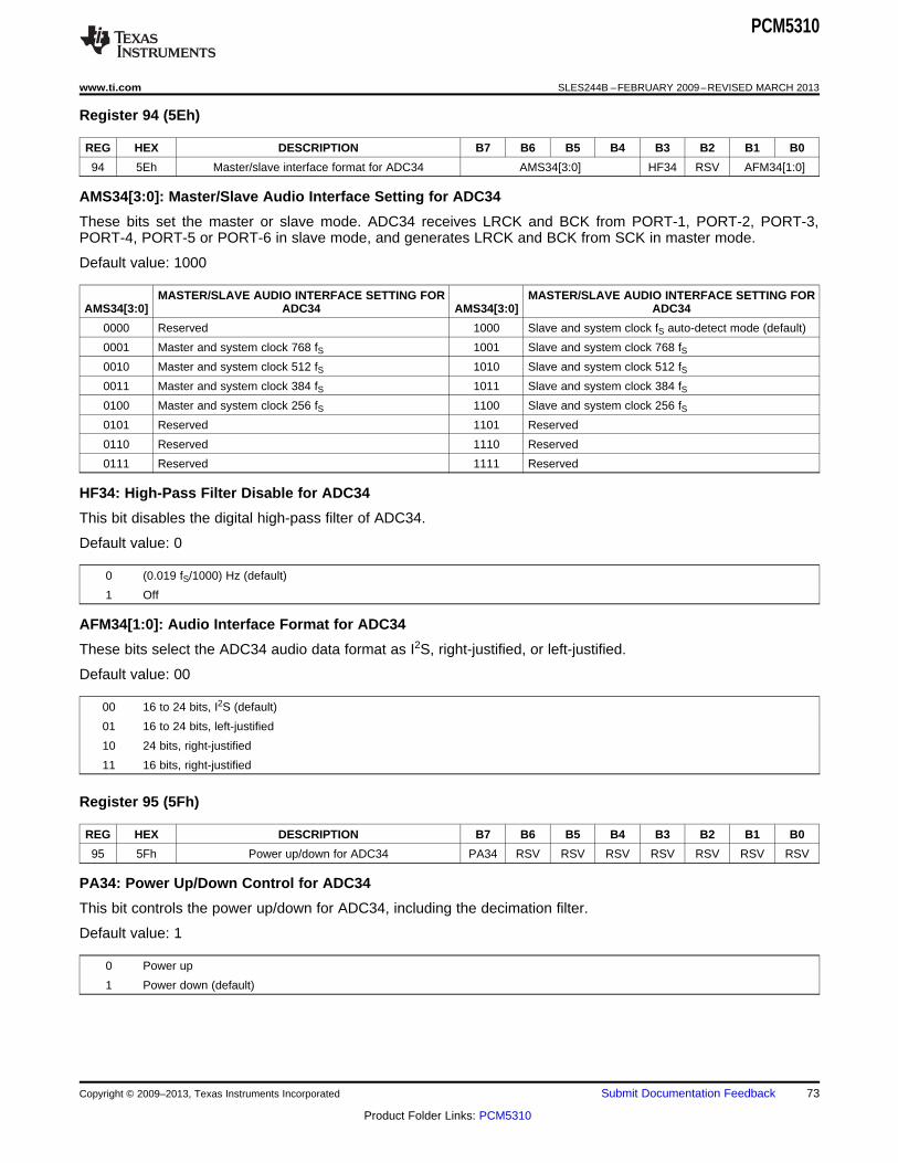
PCM5310
www.ti.com SLES244B –FEBRUARY 2009–REVISED MARCH 2013
Register 94 (5Eh)
REG HEX DESCRIPTION B7 B6 B5 B4 B3 B2 B1 B0
94 5Eh Master/slave interface format for ADC34 AMS34[3:0] HF34 RSV AFM34[1:0]
AMS34[3:0]: Master/Slave Audio Interface Setting for ADC34
These bits set the master or slave mode. ADC34 receives LRCK and BCK from PORT-1, PORT-2, PORT-3,PORT-4, PORT-5 or PORT-6 in slave mode, and generates LRCK and BCK from SCK in master mode.
Default value: 1000
MASTER/SLAVE AUDIO INTERFACE SETTING FOR MASTER/SLAVE AUDIO INTERFACE SETTING FORAMS34[3:0] ADC34 AMS34[3:0] ADC34
0000 Reserved 1000 Slave and system clock fS auto-detect mode (default)
0001 Master and system clock 768 fS 1001 Slave and system clock 768 fS
0010 Master and system clock 512 fS 1010 Slave and system clock 512 fS
0011 Master and system clock 384 fS 1011 Slave and system clock 384 fS
0100 Master and system clock 256 fS 1100 Slave and system clock 256 fS
0101 Reserved 1101 Reserved
0110 Reserved 1110 Reserved
0111 Reserved 1111 Reserved
HF34: High-Pass Filter Disable for ADC34
This bit disables the digital high-pass filter of ADC34.
Default value: 0
0 (0.019 fS/1000) Hz (default)
1 Off
AFM34[1:0]: Audio Interface Format for ADC34
These bits select the ADC34 audio data format as I2S, right-justified, or left-justified.
Default value: 00
00 16 to 24 bits, I2S (default)
01 16 to 24 bits, left-justified
10 24 bits, right-justified
11 16 bits, right-justified
Register 95 (5Fh)
REG HEX DESCRIPTION B7 B6 B5 B4 B3 B2 B1 B0
95 5Fh Power up/down for ADC34 PA34 RSV RSV RSV RSV RSV RSV RSV
PA34: Power Up/Down Control for ADC34
This bit controls the power up/down for ADC34, including the decimation filter.
Default value: 1
0 Power up
1 Power down (default)
Copyright © 2009–2013, Texas Instruments Incorporated Submit Documentation Feedback 73
Product Folder Links: PCM5310

LRCK2
BCK2
LRCK1BCK1
LRCK3BCK3
LRCK4BCK4
LRCK, BCK from ADC12 at MasterLRCK, BCK from ADC34 at MasterLRCK, BCK from DAC12 at Master
DATA from GPIO1
DATA from ADC12
LRCK, BCK from DAC34 at Master
DATA from GPIO2
DATA from ADC34
SCK2
SCK1SCK3SCK4
DATA2
DATA1DATA3DATA4
LRCK/BCK to MUX_ADCxx and MUXDACxx
SCK to MUX_ADCxx and MUXDACxx
DATA to MUXDACxx
LRCK5BCK5
LRCK6BCK6
SCK5SCK6
DATA5DATA6
MU
X-P
2B
LM
UX
-P2S
CM
UX
-P2D
T
Register 102DTS2[3:0]
Register 103SCS2[2:0]
Register 101LBS2[3:0]
PORT-2
PCM5310
SLES244B –FEBRUARY 2009–REVISED MARCH 2013 www.ti.com
Register 101 (65h)
REG HEX DESCRIPTION B7 B6 B5 B4 B3 B2 B1 B0
101 65h LRCK/BCK selection of PORT-1 and PORT-2 LBS2[3:0] LBS1[3:0]
LBS2[3:0]: LRCK/BCK Selection of PORT-2 (MUX_P2BL)
These bits are used for routing LRCK and BCK of PORT-2. Any combination of LRCK1/BCK1 to LRCK6/BCK6and LRCK/BCK of ADCs/DACs in master mode can be connected to PORT-2. Figure 47 shows a detaileddiagram of PORT-2.
Default value: 0001
0000 Output LRCK1 and BCK1
0001 Input LRCK2 and BCK2 (default)
0010 Output LRCK3 and BCK3
0011 Output LRCK4 and BCK4
0100 Output LRCK5 and BCK5
0101 Output LRCK6 and BCK6
0110 Output LRCK and BCK from DAC12 in master mode
0111 Output LRCK and BCK from DAC34 in master mode
1000 Output LRCK and BCK from ADC12 in master mode
1001 Output LRCK and BCK from ADC34 in master mode
Others Reserved
Figure 47. Detailed Diagram of PORT-2
74 Submit Documentation Feedback Copyright © 2009–2013, Texas Instruments Incorporated
Product Folder Links: PCM5310

MU
X-P
1B
L
LRCK, BCK from ADC12 at Master
LRCK, BCK from ADC34 at Master
LRCK, BCK from DAC12 at Master
LRCK, BCK from DAC34 at Master
DATA from ADC12
DATA from ADC34
LRCK/BCK to MUX_ADCxx and MUXDACxx
PORT-1
SCK to MUX_ADCxx and MUXDACxx
DATA to MUXDACxx
DATA from GPIO1
DATA from GPIO2
Register 101
LBS1[3:0]
Register 103
SCS1[2:0]
Register 102
DTS1[3:0]
LRCK1BCK1
LRCK2BCK2
LRCK3BCK3
LRCK4BCK4
LRCK5BCK5
LRCK6BCK6
SCK1
SCK2
SCK3
SCK4
SCK5
SCK6
DATA1
DATA2
DATA3
DATA4
DATA5
DATA6
MU
X-P
1S
CM
UX
-P1
DT
PCM5310
www.ti.com SLES244B –FEBRUARY 2009–REVISED MARCH 2013
LBS1[3:0]: LRCK/BCK Selection of PORT-1 (MUX_P2BL)
These bits are used for routing LRCK and BCK of PORT-1. Any combination of LRCK1/BCK1 to LRCK6/BCK6and LRCK/BCK of ADCs/DACs in master mode can be connected to PORT-1. Figure 48 shows a detaileddiagram of PORT-1.
Default value: 0000
0000 Input LRCK1 and BCK1 (default)
0001 Output LRCK2 and BCK2
0010 Output LRCK3 and BCK3
0011 Output LRCK4 and BCK4
0100 Output LRCK5 and BCK5
0101 Output LRCK6 and BCK6
0110 Output LRCK and BCK from DAC12 in master mode
0111 Output LRCK and BCK from DAC34 in master mode
1000 Output LRCK and BCK from ADC12 in master mode
1001 Output LRCK and BCK from ADC34 in master mode
Others Reserved
Figure 48. Detailed Diagram of PORT-1
Copyright © 2009–2013, Texas Instruments Incorporated Submit Documentation Feedback 75
Product Folder Links: PCM5310

PCM5310
SLES244B –FEBRUARY 2009–REVISED MARCH 2013 www.ti.com
Register 102 (66h)
REG HEX DESCRIPTION B7 B6 B5 B4 B3 B2 B1 B0
102 66h DATA selection of PORT-1 and PORT-2 DTS2[3:0] DTS1[3:0]
DTS2[3:0]: DATA Selection of PORT-2 (MUX_P2DT)
These bits are used for routing DATA of PORT-2. Any combination of DATA1 to DATA6 and DATA of ADCs inmaster mode can be connected to PORT-2. Refer to Figure 47 for more details.
Default value: 0001
0000 Output DATA1
0001 Input DATA2 (default)
0010 Output DATA3
0011 Output DATA4
0100 Output DATA5
0101 Output DATA6
0110 Output GPIO1
0111 Output GPIO2
1000 Output DATA from ADC12
1001 Output DATA from ADC34
Others Reserved
DTS1[3:0]: DATA Selection of PORT-1 (MUX_P1DT)
These bits are used for routing DATA of PORT-1. Any combination of DATA1 to DATA6 and DATA of ADCs inmaster mode can be connected to PORT-1. Refer to Figure 48 for more details.
Default value: 0000
0000 Input DATA1 (default)
0001 Output DATA2
0010 Output DATA3
0011 Output DATA4
0100 Output DATA5
0101 Output DATA6
0110 Output GPIO1
0111 Output GPIO2
1000 Output DATA from ADC12
1001 Output DATA from ADC34
Others Reserved
76 Submit Documentation Feedback Copyright © 2009–2013, Texas Instruments Incorporated
Product Folder Links: PCM5310
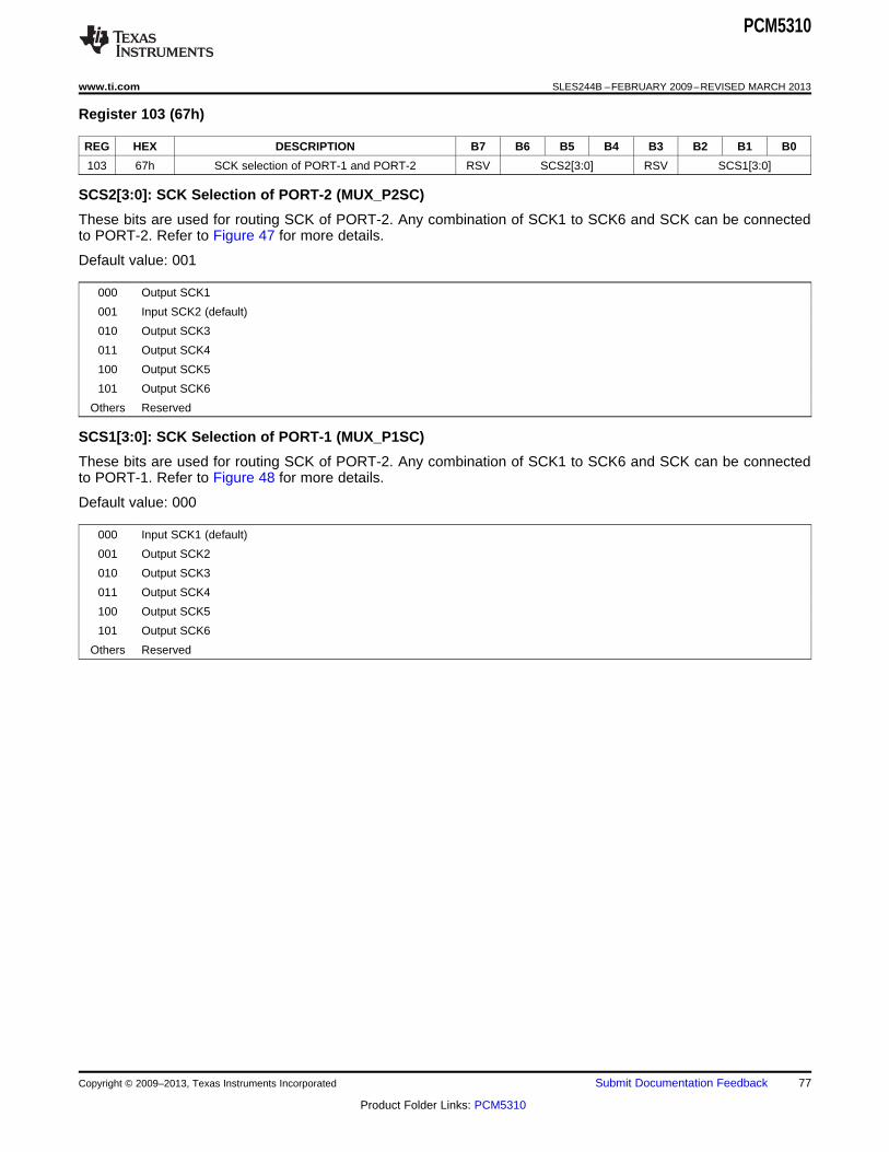
PCM5310
www.ti.com SLES244B –FEBRUARY 2009–REVISED MARCH 2013
Register 103 (67h)
REG HEX DESCRIPTION B7 B6 B5 B4 B3 B2 B1 B0
103 67h SCK selection of PORT-1 and PORT-2 RSV SCS2[3:0] RSV SCS1[3:0]
SCS2[3:0]: SCK Selection of PORT-2 (MUX_P2SC)
These bits are used for routing SCK of PORT-2. Any combination of SCK1 to SCK6 and SCK can be connectedto PORT-2. Refer to Figure 47 for more details.
Default value: 001
000 Output SCK1
001 Input SCK2 (default)
010 Output SCK3
011 Output SCK4
100 Output SCK5
101 Output SCK6
Others Reserved
SCS1[3:0]: SCK Selection of PORT-1 (MUX_P1SC)
These bits are used for routing SCK of PORT-2. Any combination of SCK1 to SCK6 and SCK can be connectedto PORT-1. Refer to Figure 48 for more details.
Default value: 000
000 Input SCK1 (default)
001 Output SCK2
010 Output SCK3
011 Output SCK4
100 Output SCK5
101 Output SCK6
Others Reserved
Copyright © 2009–2013, Texas Instruments Incorporated Submit Documentation Feedback 77
Product Folder Links: PCM5310

LRCK4
BCK4
LRCK1BCK1
LRCK2BCK2
LRCK3BCK3
LRCK, BCK from ADC12 at MasterLRCK, BCK from ADC34 at MasterLRCK, BCK from DAC12 at Master
DATA from GPIO1
DATA from ADC12
LRCK, BCK from DAC34 at Master
DATA from GPIO2
DATA from ADC34
SCK4
SCK1SCK2SCK3
DATA4
DATA1DATA2DATA3
LRCK/BCK to MUX_ADCxx and MUXDACxx
SCK to MUX_ADCxx and MUXDACxx
DATA to MUXDACxx
LRCK5BCK5
LRCK6BCK6
SCK5SCK6
DATA5DATA6
MU
X-P
4B
LM
UX
-P4S
CM
UX
-P4D
T
Register 105DTS4[3:0]
Register 106SCS1[2:0]
Register 104LBS4[3:0]
PORT-4
PCM5310
SLES244B –FEBRUARY 2009–REVISED MARCH 2013 www.ti.com
Register 104 (68h)
REG HEX DESCRIPTION B7 B6 B5 B4 B3 B2 B1 B0
104 68h LRCK/BCK selection of PORT-3 and PORT-4 LBS4[3:0] LBS3[3:0]
LBS4[3:0]: LRCK/BCK Selection of PORT-4 (MUX_P4BL)
These bits are used for routing LRCK and BCK of PORT-4. Any combination of LRCK1/BCK1 to LRCK6/BCK6and LRCK/BCK of ADCs/DACs in master mode can be connected to PORT-4. Figure 49 shows a detaileddiagram of PORT-4.
Default value: 0011
0000 Output LRCK1 and BCK1
0001 Output LRCK2 and BCK2
0010 Output LRCK3 and BCK3
0011 Input LRCK4 and BCK4 (default)
0100 Output LRCK5 and BCK5
0101 Output LRCK6 and BCK6
0110 Output LRCK and BCK from DAC12 in master mode
0111 Output LRCK and BCK from DAC34 in master mode
1000 Output LRCK and BCK from ADC12 in master mode
1001 Output LRCK and BCK from ADC34 in master mode
Others Reserved
Figure 49. Detailed Diagram of PORT-4
78 Submit Documentation Feedback Copyright © 2009–2013, Texas Instruments Incorporated
Product Folder Links: PCM5310

LRCK3
BCK3
LRCK1BCK1
LRCK2BCK2
LRCK4BCK4
LRCK, BCK from ADC12 at MasterLRCK, BCK from ADC34 at MasterLRCK, BCK from DAC12 at Master
DATA from GPIO1
DATA from ADC12
LRCK, BCK from DAC34 at Master
DATA from GPIO2
DATA from ADC34
SCK3
SCK1SCK2SCK4
DATA3
DATA1DATA2DATA4
LRCK/BCK to MUX_ADCxx and MUXDACxx
SCK to MUX_ADCxx and MUXDACxx
DATA to MUXDACxx
LRCK5BCK5
LRCK6BCK6
SCK5SCK6
DATA5DATA6
MU
X-P
4B
LM
UX
-P3S
CM
UX
-P3D
T
Register 105DTS3[3:0]
Register 106SCS3[2:0]
Register 104LBS3[3:0]
PORT-3
PCM5310
www.ti.com SLES244B –FEBRUARY 2009–REVISED MARCH 2013
LBS3[3:0]: LRCK/BCK Selection of PORT-3 (MUX_P3BL)
These bits are used for routing LRCK and BCK of PORT-3. Any combination of LRCK1/BCK1 to LRCK6/BCK6and LRCK/BCK of ADCs/DACs in master mode can be connected to PORT-3. Figure 50 shows a detaileddiagram of PORT-3.
Default value: 0010
0000 Output LRCK1 and BCK1
0001 Output LRCK2 and BCK2
0010 Input LRCK3 and BCK3 (default)
0011 Output LRCK4 and BCK4
0100 Output LRCK5 and BCK5
0101 Output LRCK6 and BCK6
0110 Output LRCK and BCK from DAC12 in master mode
0111 Output LRCK and BCK from DAC34 in master mode
1000 Output LRCK and BCK from ADC12 in master mode
1001 Output LRCK and BCK from ADC34 in master mode
Others Reserved
Figure 50. Detailed Diagram of PORT-3
Copyright © 2009–2013, Texas Instruments Incorporated Submit Documentation Feedback 79
Product Folder Links: PCM5310

PCM5310
SLES244B –FEBRUARY 2009–REVISED MARCH 2013 www.ti.com
Register 105 (69h)
REG HEX DESCRIPTION B7 B6 B5 B4 B3 B2 B1 B0
105 69h DATA selection of PORT-3 and PORT-4 DTS4[3:0] DTS3[3:0]
DTS4[3:0]: DATA Selection of PORT-4 (MUX_P4DT)
These bits are used for routing DATA of PORT-4. Any combination of DATA1 to DATA6 and DATA of ADCs inmaster mode can be connected to PORT-4. Refer to Figure 49 for more details.
Default value: 0011
0000 Output DATA1
0001 Output DATA2
0010 Output DATA3
0011 Input DATA4 (default)
0100 Output DATA5
0101 Output DATA6
0110 Output GPIO1
0111 Output GPIO2
1000 Output DATA from ADC12
1001 Output DATA from ADC34
Others Reserved
DTS3[3:0]: DATA Selection of PORT-3 (MUX_P3DT)
These bits are used for routing DATA of PORT-3. Any combination of DATA1 to DATA6 and DATA of ADCs inmaster mode can be connected to PORT-3. Refer to Figure 50 for more details.
Default value: 0010
0000 Output DATA1
0001 Output DATA2
0010 Input DATA3 (default)
0011 Output DATA4
0100 Output DATA5
0101 Output DATA6
0110 Output GPIO1
0111 Output GPIO2
1000 Output DATA from ADC12
1001 Output DATA from ADC34
Others Reserved
80 Submit Documentation Feedback Copyright © 2009–2013, Texas Instruments Incorporated
Product Folder Links: PCM5310

PCM5310
www.ti.com SLES244B –FEBRUARY 2009–REVISED MARCH 2013
Register 106 (6Ah)
REG HEX DESCRIPTION B7 B6 B5 B4 B3 B2 B1 B0
106 6Ah SCK selection of PORT-3 and PORT-4 RSV SCS4[3:0] RSV SCS3[3:0]
SCS4[3:0]: SCK Selection of PORT-4 (MUX_P4SC)
These bits are used for routing SCK of PORT-4. Any combination of SCK1 to SCK6 and SCK can be connectedto PORT-4. Refer to Figure 49 for more details.
Default value: 011
000 Output SCK1
001 Output SCK2
010 Output SCK3
011 Input SCK4 (default)
100 Output SCK5
101 Output SCK6
Others Reserved
SCS3[3:0]: SCK Selection of PORT-3 (MUX_P3SC)
These bits are used for routing SCK of PORT-3. Any combination of SCK1 to SCK6 and SCK can be connectedto PORT-3. Refer to Figure 50 for more details.
Default value: 010
000 Output SCK1
001 Output SCK2
010 Input SCK3 (default)
011 Output SCK4
100 Output SCK5
101 Output SCK6
Others Reserved
Copyright © 2009–2013, Texas Instruments Incorporated Submit Documentation Feedback 81
Product Folder Links: PCM5310

LRCK6
BCK6
LRCK1BCK1
LRCK2BCK2
LRCK3BCK3
LRCK, BCK from ADC12 at MasterLRCK, BCK from ADC34 at MasterLRCK, BCK from DAC12 at Master
DATA from GPIO1
DATA from ADC12
LRCK, BCK from DAC34 at Master
DATA from GPIO2
DATA from ADC34
SCK6
SCK1SCK2SCK3
DATA6
DATA1DATA2DATA3
LRCK/BCK to MUX_ADCxx and MUXDACxx
SCK to MUX_ADCxx and MUXDACxx
DATA to MUXDACxx
LRCK4BCK4
LRCK5BCK5
SCK4SCK5
DATA4DATA5
MU
X-P
6B
LM
UX
-P6S
CM
UX
-P6D
T
Register 108DTS6[3:0]
Register 109SCS6[2:0]
Register 107LBS6[3:0]
PORT-6
PCM5310
SLES244B –FEBRUARY 2009–REVISED MARCH 2013 www.ti.com
Register 107 (6Bh)
REG HEX DESCRIPTION B7 B6 B5 B4 B3 B2 B1 B0
107 6Bh LRCK/BCK selection of PORT-5 and PORT-6 LBS6[3:0] LBS5[3:0]
LBS6[3:0]: LRCK/BCK Selection of PORT-6 (MUX_P6BL)
These bits are used for routing LRCK and BCK of PORT-6. Any combination of LRCK1/BCK1 to LRCK6/BCK6and LRCK/BCK of ADCs/DACs in master mode can be connected to PORT-6. Figure 51 shows a detaileddiagram of PORT-6.
Default value: 0101
0000 Output LRCK1 and BCK1
0001 Output LRCK2 and BCK2
0010 Output LRCK3 and BCK3
0011 Output LRCK4 and BCK4
0100 Output LRCK5 and BCK5
0101 Input LRCK6 and BCK6 (default)
0110 Output LRCK and BCK from DAC12 in master mode
0111 Output LRCK and BCK from DAC34 in master mode
1000 Output LRCK and BCK from ADC12 in master mode
1001 Output LRCK and BCK from ADC34 in master mode
Others Reserved
Figure 51. Detailed Diagram of PORT-6
82 Submit Documentation Feedback Copyright © 2009–2013, Texas Instruments Incorporated
Product Folder Links: PCM5310

LRCK5
BCK5
LRCK1BCK1
LRCK2BCK2
LRCK3BCK3
LRCK, BCK from ADC12 at MasterLRCK, BCK from ADC34 at MasterLRCK, BCK from DAC12 at Master
DATA from GPIO1
DATA from ADC12
LRCK, BCK from DAC34 at Master
DATA from GPIO2
DATA from ADC34
SCK5
SCK1SCK2SCK3
DATA5
DATA1DATA2DATA3
LRCK/BCK to MUX_ADCxx and MUXDACxx
SCK to MUX_ADCxx and MUXDACxx
DATA to MUXDACxx
LRCK4BCK4
LRCK6BCK6
SCK4SCK6
DATA4DATA6
MU
X-P
5B
LM
UX
-P5S
CM
UX
-P5D
T
Register 108DTS5[3:0]
Register 109SCS5[2:0]
Register 107LBS5[3:0]
PORT-5
PCM5310
www.ti.com SLES244B –FEBRUARY 2009–REVISED MARCH 2013
LBS5[3:0]: LRCK/BCK Selection of PORT-5 (MUX_P5BL)
These bits are used for routing LRCK and BCK of PORT-5. Any combination of LRCK1/BCK1 to LRCK6/BCK6and LRCK/BCK of ADCs/DACs in master mode can be connected to PORT-5. Figure 52 shows a detaileddiagram of PORT-5.
Default value: 0100
0000 Output LRCK1 and BCK1
0001 Output LRCK2 and BCK2
0010 Output LRCK3 and BCK3
0011 Output LRCK4 and BCK4
0100 Input LRCK5 and BCK5 (default)
0101 Output LRCK6 and BCK6
0110 Output LRCK and BCK from DAC12 in master mode
0111 Output LRCK and BCK from DAC34 in master mode
1000 Output LRCK and BCK from ADC12 in master mode
1001 Output LRCK and BCK from ADC34 in master mode
Others Reserved
Figure 52. Detailed Diagram of PORT-5
Copyright © 2009–2013, Texas Instruments Incorporated Submit Documentation Feedback 83
Product Folder Links: PCM5310
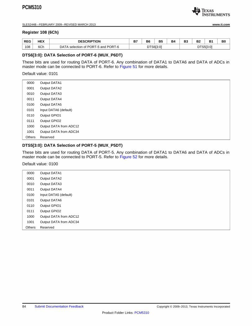
PCM5310
SLES244B –FEBRUARY 2009–REVISED MARCH 2013 www.ti.com
Register 108 (6Ch)
REG HEX DESCRIPTION B7 B6 B5 B4 B3 B2 B1 B0
108 6Ch DATA selection of PORT-5 and PORT-6 DTS6[3:0] DTS5[3:0]
DTS6[3:0]: DATA Selection of PORT-6 (MUX_P6DT)
These bits are used for routing DATA of PORT-6. Any combination of DATA1 to DATA6 and DATA of ADCs inmaster mode can be connected to PORT-6. Refer to Figure 51 for more details.
Default value: 0101
0000 Output DATA1
0001 Output DATA2
0010 Output DATA3
0011 Output DATA4
0100 Output DATA5
0101 Input DATA6 (default)
0110 Output GPIO1
0111 Output GPIO2
1000 Output DATA from ADC12
1001 Output DATA from ADC34
Others Reserved
DTS5[3:0]: DATA Selection of PORT-5 (MUX_P5DT)
These bits are used for routing DATA of PORT-5. Any combination of DATA1 to DATA6 and DATA of ADCs inmaster mode can be connected to PORT-5. Refer to Figure 52 for more details.
Default value: 0100
0000 Output DATA1
0001 Output DATA2
0010 Output DATA3
0011 Output DATA4
0100 Input DATA5 (default)
0101 Output DATA6
0110 Output GPIO1
0111 Output GPIO2
1000 Output DATA from ADC12
1001 Output DATA from ADC34
Others Reserved
84 Submit Documentation Feedback Copyright © 2009–2013, Texas Instruments Incorporated
Product Folder Links: PCM5310

PCM5310
www.ti.com SLES244B –FEBRUARY 2009–REVISED MARCH 2013
Register 109 (6Dh)
REG HEX DESCRIPTION B7 B6 B5 B4 B3 B2 B1 B0
109 6Dh SCK selection of PORT-5 and PORT-6 RSV SCS6[3:0] RSV SCS5[3:0]
SCS6[3:0]: SCK Selection of PORT-6 (MUX_P6SC)
These bits are used for routing SCK of PORT-6. Any combination of SCK1 to SCK6 and SCK can be connectedto PORT-6. Refer to Figure 51 for more details.
Default value: 101
000 Output SCK1
001 Output SCK2
010 Output SCK3
011 Output SCK4
100 Output SCK5
101 Input SCK6 (default)
Others Reserved
SCS5[3:0]: SCK Selection of PORT-5 (MUX_P5SC)
These bits are used for routing SCK of PORT-5. Any combination of SCK1 to SCK6 and SCK can be connectedto PORT-5. Refer to Figure 52 for more details.
Default value: 100
000 Output SCK1
001 Output SCK2
010 Output SCK3
011 Output SCK4
100 Input SCK5 (default)
101 Output SCK6
Others Reserved
Copyright © 2009–2013, Texas Instruments Incorporated Submit Documentation Feedback 85
Product Folder Links: PCM5310

PCM5310
SLES244B –FEBRUARY 2009–REVISED MARCH 2013 www.ti.com
Register 110 (6Eh)
REG HEX DESCRIPTION B7 B6 B5 B4 B3 B2 B1 B0
110 6Eh LRCK/BCK selection of DAC12 and DAC34 D34LB[3:0] D12LB[3:0]
D34LB[3:0]: LRCK/BCK Selection of DAC34 (MUX_DA34)
These bits are used for routing LRCK and BCK from each audio interface port to DAC34, or routing LRCK andBCK from DACs/ADCs to each audio interface port in master mode. Refer to Figure 33 for more details.
Default value: 0100
0000 Select LRCK and BCK from PORT-1
0001 Select LRCK and BCK from PORT-2
0010 Select LRCK and BCK from PORT-3
0011 Select LRCK and BCK from PORT-4
0100 Select LRCK and BCK from PORT-5 (default)
0101 Select LRCK and BCK from PORT-6
0110 Select LRCK and BCK from DAC12 in master mode
0111 Select LRCK and BCK from DAC34 in master mode
1000 Select LRCK and BCK from ADC12 in master mode
1001 Select LRCK and BCK from ADC34 in master mode
Others Reserved
D12LB[3:0] LRCK/BCK Selection of DAC12 (MUX_DA12)
These bits are used for routing LRCK and BCK from each audio interface port to DAC12, or routing LRCK andBCK from DACs/ADCs to each audio interface port in master mode. Refer to Figure 33 for more details.
Default value: 0011
0000 Select LRCK and BCK from PORT-1
0001 Select LRCK and BCK from PORT-2
0010 Select LRCK and BCK from PORT-3
0011 Select LRCK and BCK from PORT-4 (default)
0100 Select LRCK and BCK from PORT-5
0101 Select LRCK and BCK from PORT-6
0110 Select LRCK and BCK from DAC12 in master mode
0111 Select LRCK and BCK from DAC34 in master mode
1000 Select LRCK and BCK from ADC12 in master mode
1001 Select LRCK and BCK from ADC34 in master mode
Others Reserved
86 Submit Documentation Feedback Copyright © 2009–2013, Texas Instruments Incorporated
Product Folder Links: PCM5310
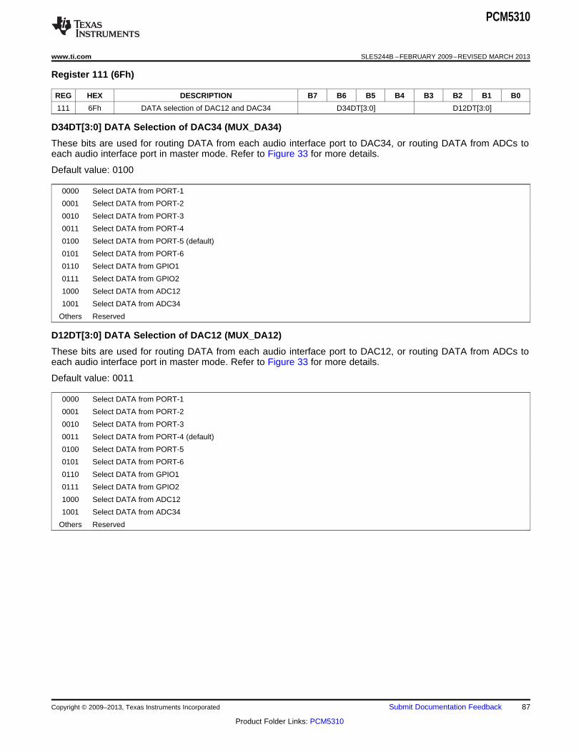
PCM5310
www.ti.com SLES244B –FEBRUARY 2009–REVISED MARCH 2013
Register 111 (6Fh)
REG HEX DESCRIPTION B7 B6 B5 B4 B3 B2 B1 B0
111 6Fh DATA selection of DAC12 and DAC34 D34DT[3:0] D12DT[3:0]
D34DT[3:0] DATA Selection of DAC34 (MUX_DA34)
These bits are used for routing DATA from each audio interface port to DAC34, or routing DATA from ADCs toeach audio interface port in master mode. Refer to Figure 33 for more details.
Default value: 0100
0000 Select DATA from PORT-1
0001 Select DATA from PORT-2
0010 Select DATA from PORT-3
0011 Select DATA from PORT-4
0100 Select DATA from PORT-5 (default)
0101 Select DATA from PORT-6
0110 Select DATA from GPIO1
0111 Select DATA from GPIO2
1000 Select DATA from ADC12
1001 Select DATA from ADC34
Others Reserved
D12DT[3:0] DATA Selection of DAC12 (MUX_DA12)
These bits are used for routing DATA from each audio interface port to DAC12, or routing DATA from ADCs toeach audio interface port in master mode. Refer to Figure 33 for more details.
Default value: 0011
0000 Select DATA from PORT-1
0001 Select DATA from PORT-2
0010 Select DATA from PORT-3
0011 Select DATA from PORT-4 (default)
0100 Select DATA from PORT-5
0101 Select DATA from PORT-6
0110 Select DATA from GPIO1
0111 Select DATA from GPIO2
1000 Select DATA from ADC12
1001 Select DATA from ADC34
Others Reserved
Copyright © 2009–2013, Texas Instruments Incorporated Submit Documentation Feedback 87
Product Folder Links: PCM5310

PCM5310
SLES244B –FEBRUARY 2009–REVISED MARCH 2013 www.ti.com
Register 112 (70h)
REG HEX DESCRIPTION B7 B6 B5 B4 B3 B2 B1 B0
112 70h SCK selection of DAC12 and DAC34 RSV D34SC[3:0] RSV D12SC[3:0]
D34SC[2:0] SCK Selection of DAC34 (MUX_DA34)
These bits are used for routing SCK from each audio interface port to DAC34. Refer to Figure 33 for moredetails.
Default value: 100
000 Select SCK from PORT-1
001 Select SCK from PORT-2
010 Select SCK from PORT-3
011 Select SCK from PORT-4
100 Select SCK from PORT-5 (default)
101 Select SCK from PORT-6
Others Reserved
D12SC[2:0] SCK Selection of DAC12 (MUX_DA12)
These bits are used for routing SCK from each audio interface port to DAC12. Refer to Figure 33 for moredetails.
Default value: 011
000 Select SCK from PORT-1
001 Select SCK from PORT-2
010 Select SCK from PORT-3
011 Select SCK from PORT-4 (default)
100 Select SCK from PORT-5
101 Select SCK from PORT-6
Others Reserved
88 Submit Documentation Feedback Copyright © 2009–2013, Texas Instruments Incorporated
Product Folder Links: PCM5310

PCM5310
www.ti.com SLES244B –FEBRUARY 2009–REVISED MARCH 2013
Register 116 (74h)
REG HEX DESCRIPTION B7 B6 B5 B4 B3 B2 B1 B0
116 74h LRCK/BCK selection of ADC12 and ADC34 A34LB[3:0] A12LB[3:0]
A34LB[3:0]: LRCK/BCK Selection of ADC34 (MUX_AD34)
These bits are used for routing LRCK and BCK from each audio interface port to ADC34, or routing LRCK andBCK from DACs/ADCs to each audio interface port in master mode. Refer to Figure 33 for more details.
Default value: 0001
0000 Select LRCK and BCK from PORT-1
0001 Select LRCK and BCK from PORT-2 (default)
0010 Select LRCK and BCK from PORT-3
0011 Select LRCK and BCK from PORT-4
0100 Select LRCK and BCK from PORT-5
0101 Select LRCK and BCK from PORT-6
0110 Select LRCK and BCK from DAC12 in master mode
0111 Select LRCK and BCK from DAC34 in master mode
1000 Select LRCK and BCK from ADC12 in master mode
1001 Select LRCK and BCK from ADC34 in master mode
Others Reserved
A12LB[3:0] LRCK/BCK Selection of ADC12 (MUX_AD12)
These bits are used for routing LRCK and BCK from each audio interface port to ADC12, or routing LRCK andBCK from DACs/ADCs to each audio interface port in master mode. Refer to Figure 33 for more details.
Default value: 0000
0000 Select LRCK and BCK from PORT-1 (default)
0001 Select LRCK and BCK from PORT-2
0010 Select LRCK and BCK from PORT-3
0011 Select LRCK and BCK from PORT-4
0100 Select LRCK and BCK from PORT-5
0101 Select LRCK and BCK from PORT-6
0110 Select LRCK and BCK from DAC12 in master mode
0111 Select LRCK and BCK from DAC34 in master mode
1000 Select LRCK and BCK from ADC12 in master mode
1001 Select LRCK and BCK from ADC34 in master mode
Others Reserved
Copyright © 2009–2013, Texas Instruments Incorporated Submit Documentation Feedback 89
Product Folder Links: PCM5310

PCM5310
SLES244B –FEBRUARY 2009–REVISED MARCH 2013 www.ti.com
Register 117 (75h)
REG HEX DESCRIPTION B7 B6 B5 B4 B3 B2 B1 B0
117 75h SCK selection of ADC12 and ADC34 RSV A34SC[3:0] RSV A12SC[3:0]
A34SC[2:0] SCK Selection of ADC34 (MUX_AD34)
These bits are used for routing SCK from each audio interface port to ADC34. Refer to Figure 33 for moredetails.
Default value: 001
000 Select SCK from PORT-1
001 Select SCK from PORT-2 (default)
010 Select SCK from PORT-3
011 Select SCK from PORT-4
100 Select SCK from PORT-5
101 Select SCK from PORT-6
Others Reserved
A12SC[2:0] SCK Selection of ADC12 (MUX_AD12)
These bits are used for routing SCK from each audio interface port to ADC12. Refer to Figure 33 for moredetails.
Default value: 000
000 Select SCK from PORT-1 (default)
001 Select SCK from PORT-2
010 Select SCK from PORT-3
011 Select SCK from PORT-4
100 Select SCK from PORT-5
101 Select SCK from PORT-6
Others Reserved
90 Submit Documentation Feedback Copyright © 2009–2013, Texas Instruments Incorporated
Product Folder Links: PCM5310
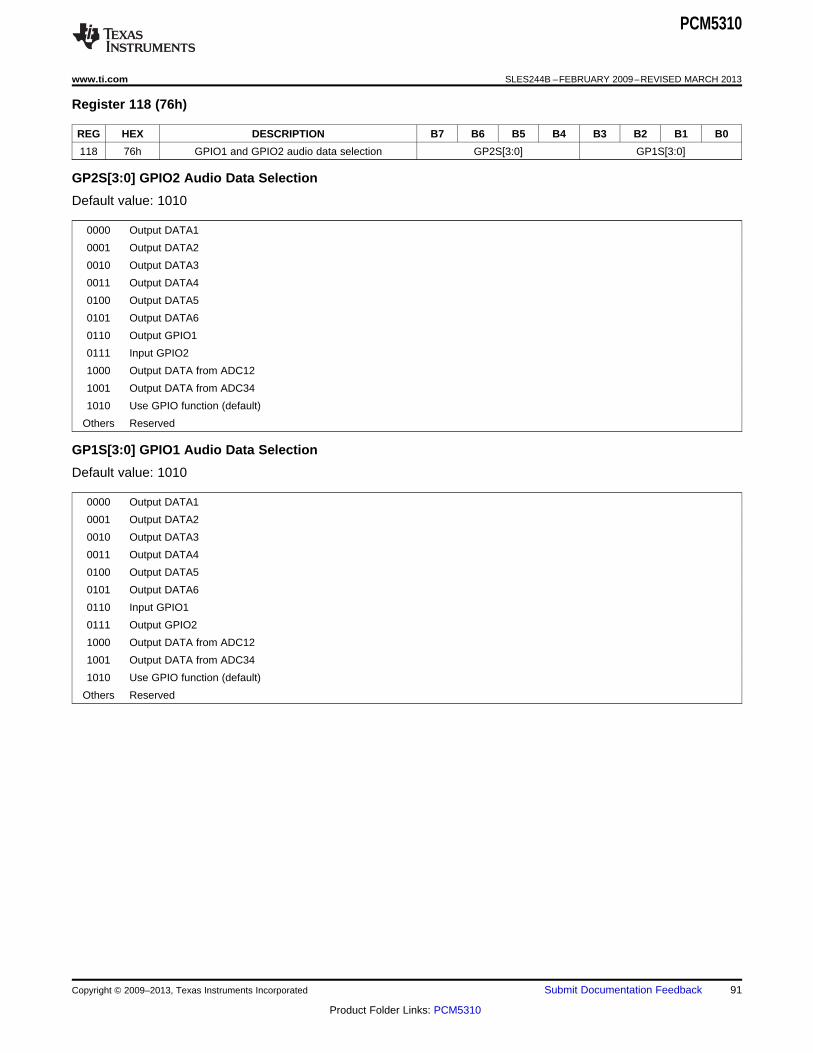
PCM5310
www.ti.com SLES244B –FEBRUARY 2009–REVISED MARCH 2013
Register 118 (76h)
REG HEX DESCRIPTION B7 B6 B5 B4 B3 B2 B1 B0
118 76h GPIO1 and GPIO2 audio data selection GP2S[3:0] GP1S[3:0]
GP2S[3:0] GPIO2 Audio Data Selection
Default value: 1010
0000 Output DATA1
0001 Output DATA2
0010 Output DATA3
0011 Output DATA4
0100 Output DATA5
0101 Output DATA6
0110 Output GPIO1
0111 Input GPIO2
1000 Output DATA from ADC12
1001 Output DATA from ADC34
1010 Use GPIO function (default)
Others Reserved
GP1S[3:0] GPIO1 Audio Data Selection
Default value: 1010
0000 Output DATA1
0001 Output DATA2
0010 Output DATA3
0011 Output DATA4
0100 Output DATA5
0101 Output DATA6
0110 Input GPIO1
0111 Output GPIO2
1000 Output DATA from ADC12
1001 Output DATA from ADC34
1010 Use GPIO function (default)
Others Reserved
Copyright © 2009–2013, Texas Instruments Incorporated Submit Documentation Feedback 91
Product Folder Links: PCM5310

AIN1L (1)
AIN1R (2)
AIN2L (3)
AIN2R (4)
AIN3L (5)
AIN3R (6)
AIN4L (7)
AIN4R (8)
AIN5L (9)
AIN5R (10)
AIN6L (11)
AIN6R (12)
(13) LO1L
(14) LO1R
(15) LO2L
(16) LO2R
(19) HPOL
(22) HPOR
(25) VCOMDA
(64) VCOMAD
(62) VREFAD1
(63) VREFAD2
(58) RSTB
(59) AMUTE
(27) SDA
(28) SCL
(55) GPIO1
(26) GPIO2
(27) GPIO3
(26) AGNDS
SCK1 (29)
BCK1 (30)
LRCK1 (31)
DATA1 (32)
SCK2 (33)
BCK2 (34)
LRCK2 (35)
DATA2 (36)
SCK3 (37)
BCK3 (38)
LRCK3 (39)
DATA3 (40)
SCK4 (43)
BCK4 (44)
LRCK4 (45)
DATA4 (46)
SCK5 (47)
BCK5 (48)
LRCK5 (49)
DATA5 (50)
SCK6 (51)
BCK6 (52)
LRCK6 (53)
DATA6 (54)
22 to 100W W
External Circuit
External Circuit
External Circuit
External Circuit
External Circuit
External Circuit
External Circuit
External Circuit
External Circuit
External Circuit
External Circuit
Line
Input
Control
Interface
Audio Interface
and Clocks
(1) (2)
External Circuit
External Circuit
External Circuit
External Circuit
External Circuit
+ 1.0 Fm+ 1.0 Fm
+ 1.0 Fm
(41) VDD
(42) DGND
(23) VCCDA
(24) AGNDDA
(60) VCCAD
(61) AGNDAD
(20) VCCP
(21) PGND
(18) VCCH
(17) HGND
+
+
+
+
+
3.3 V
9.0 V
> 4.7 Fm
> 4.7 Fm
> 4.7 Fm
> 4.7 Fm
> 4.7 Fm
Power
Supply
Reference
Voltage
(3)
Line
Output
Headphone
Output
External Circuit
External Circuit
PCM5310
SLES244B –FEBRUARY 2009–REVISED MARCH 2013 www.ti.com
BASIC CONNECTION DIAGRAMS
(1) See Figure 54 for the line input.
(2) See Figure 55 for the line output.
(3) See Figure 56 for the headphone output.
Figure 53. Basic Connections
92 Submit Documentation Feedback Copyright © 2009–2013, Texas Instruments Incorporated
Product Folder Links: PCM5310

+
47 k (typ)W
R1
R3C1
C3 To ADC47 k (typ)W
AINL (1)
+
47 k (typ)W
R2
R4C2
C4 To ADC47 k (typ)W
AINR (2)
(a) External Circuit for Line Input with Low-Pass Filter
+
47 k (typ)W
C5
To ADC47 k (typ)W
AINL (1)
+
47 k (typ)W
C6
To ADC47 k (typ)W
AINR (2)
(b) External Circuit for Line Input without Low-Pass Filter
47 k (typ)W
C7
To ADC47 k (typ)W
AINL (1)
47 k (typ)W
To ADC47 k (typ)W
AINR (2)
(c) External Circuit for not using Analog Input
PCM5310
www.ti.com SLES244B –FEBRUARY 2009–REVISED MARCH 2013
R1, R2: Greater than 100 kΩR3, R4: 100 Ω to 1 kΩC1, C2, C5, C6: 1 μF to 47 μFC3, C4: 0.01 μF to 0.001 μFC7: Less than 0.1 μF
Figure 54. External Circuit for the Line Input
Copyright © 2009–2013, Texas Instruments Incorporated Submit Documentation Feedback 93
Product Folder Links: PCM5310

+From DAC
C1 R1
C3
Mute
Circuit
HPOL (19)
R3
+
From DACC2 R2
C4
Mute
Circuit
HPOR (20)
R4
+
From DACC5
C7
Mute
Circuit
HPOL (19)
R5
+
From DACC6
C8
Mute
Circuit
HPOR (20)
R6
(a) External Circuit with Short-Circuit protection Resistor (b) External Circuit without Short-Circuit Protection Resistor
(a) External Circuit for Line Output with Low-Pass Filter (b) External Circuit for Line Output with Low-Pass Filter
+
R3
R1
C3
From DACC1
Mute
Circuit
LO1L (13)
+
R4
R2
C4
From DACC2
Mute
Circuit
LO1R (14)
f = 85 kHzC
+ R5
From DACC5
C7
Mute
Circuit
LO1L (13)
+From DAC
LO1R (14)
f = 85 kHzC
R7
R6C6
C8
Mute
Circuit
R8
PCM5310
SLES244B –FEBRUARY 2009–REVISED MARCH 2013 www.ti.com
R1, R2, R5, R6: 270 ΩR3, R4, R7: > 100 kΩC1, C2, C5, C6: 1 μF to 47 μFC3, C4, C7, C8: 6800 pF
Figure 55. External Circuit for the Line Output
R1, R2 : 4 Ω to 16 ΩR3, R4, R5, R6 : 22 ΩC1, C2, C5, C6: 47 μF to 220 μFC3, C4, C7, C8 : 0.022 μF
Figure 56. External Circuit for the Headphone Output
94 Submit Documentation Feedback Copyright © 2009–2013, Texas Instruments Incorporated
Product Folder Links: PCM5310
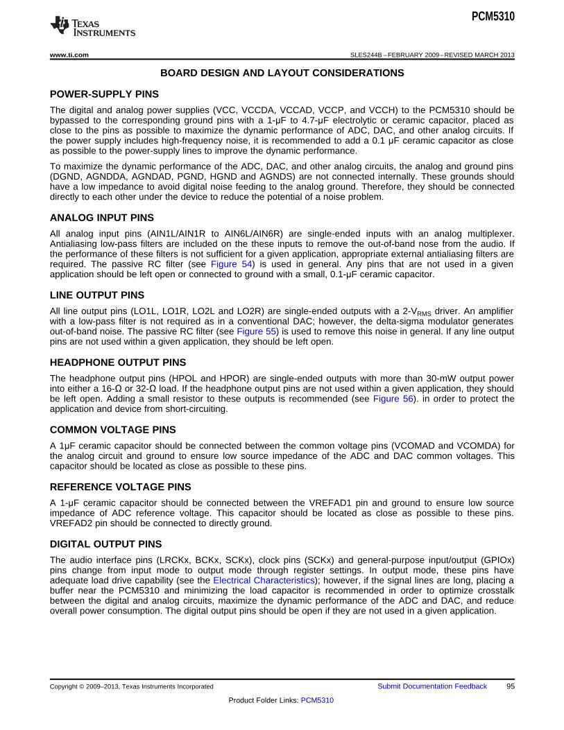
PCM5310
www.ti.com SLES244B –FEBRUARY 2009–REVISED MARCH 2013
BOARD DESIGN AND LAYOUT CONSIDERATIONS
POWER-SUPPLY PINS
The digital and analog power supplies (VCC, VCCDA, VCCAD, VCCP, and VCCH) to the PCM5310 should bebypassed to the corresponding ground pins with a 1-μF to 4.7-μF electrolytic or ceramic capacitor, placed asclose to the pins as possible to maximize the dynamic performance of ADC, DAC, and other analog circuits. Ifthe power supply includes high-frequency noise, it is recommended to add a 0.1 μF ceramic capacitor as closeas possible to the power-supply lines to improve the dynamic performance.
To maximize the dynamic performance of the ADC, DAC, and other analog circuits, the analog and ground pins(DGND, AGNDDA, AGNDAD, PGND, HGND and AGNDS) are not connected internally. These grounds shouldhave a low impedance to avoid digital noise feeding to the analog ground. Therefore, they should be connecteddirectly to each other under the device to reduce the potential of a noise problem.
ANALOG INPUT PINS
All analog input pins (AIN1L/AIN1R to AIN6L/AIN6R) are single-ended inputs with an analog multiplexer.Antialiasing low-pass filters are included on the these inputs to remove the out-of-band nose from the audio. Ifthe performance of these filters is not sufficient for a given application, appropriate external antialiasing filters arerequired. The passive RC filter (see Figure 54) is used in general. Any pins that are not used in a givenapplication should be left open or connected to ground with a small, 0.1-μF ceramic capacitor.
LINE OUTPUT PINS
All line output pins (LO1L, LO1R, LO2L and LO2R) are single-ended outputs with a 2-VRMS driver. An amplifierwith a low-pass filter is not required as in a conventional DAC; however, the delta-sigma modulator generatesout-of-band noise. The passive RC filter (see Figure 55) is used to remove this noise in general. If any line outputpins are not used within a given application, they should be left open.
HEADPHONE OUTPUT PINS
The headphone output pins (HPOL and HPOR) are single-ended outputs with more than 30-mW output powerinto either a 16-Ω or 32-Ω load. If the headphone output pins are not used within a given application, they shouldbe left open. Adding a small resistor to these outputs is recommended (see Figure 56). in order to protect theapplication and device from short-circuiting.
COMMON VOLTAGE PINS
A 1μF ceramic capacitor should be connected between the common voltage pins (VCOMAD and VCOMDA) forthe analog circuit and ground to ensure low source impedance of the ADC and DAC common voltages. Thiscapacitor should be located as close as possible to these pins.
REFERENCE VOLTAGE PINS
A 1-μF ceramic capacitor should be connected between the VREFAD1 pin and ground to ensure low sourceimpedance of ADC reference voltage. This capacitor should be located as close as possible to these pins.VREFAD2 pin should be connected to directly ground.
DIGITAL OUTPUT PINS
The audio interface pins (LRCKx, BCKx, SCKx), clock pins (SCKx) and general-purpose input/output (GPIOx)pins change from input mode to output mode through register settings. In output mode, these pins haveadequate load drive capability (see the Electrical Characteristics); however, if the signal lines are long, placing abuffer near the PCM5310 and minimizing the load capacitor is recommended in order to optimize crosstalkbetween the digital and analog circuits, maximize the dynamic performance of the ADC and DAC, and reduceoverall power consumption. The digital output pins should be open if they are not used in a given application.
Copyright © 2009–2013, Texas Instruments Incorporated Submit Documentation Feedback 95
Product Folder Links: PCM5310

PCM5310
SLES244B –FEBRUARY 2009–REVISED MARCH 2013 www.ti.com
DIGITAL INPUT PINS
Series resistors (ranging from 22 Ω to 100 Ω) are recommended for the SCKx, LRCKx, BCKx, and DATAx pins.These series resistors combine with the stray printed circuit board (PCB) and device input capacitance to form alow-pass filter that removes high-frequency noise from the digital signal, thus reducing high-frequency emissions.All digital input pins should be connected to ground if they are not used in a given application.
PowerPAD (THERMAL PAD)
The PCM5310 is available in an HTQFP-64 PowerPAD package. The PowerPAD is a heatsink, which is exposedmetal at the bottom of the package. The PowerPAD works to conduct heat away from the silicon through thermalvias located at the bottom of the PowerPAD.
The PowerPAD does not need to be soldered onto an exposed metal area of the PCB because the device workswithin the absolute maximum rating (junction temperature = +150°C) without soldering the PowerPAD.
Refer to application note SLMA002, PowerPAD Thermally Enhanced Package, when considering whether tosolder the PowerPAD in order to reduce more heat from the device.
96 Submit Documentation Feedback Copyright © 2009–2013, Texas Instruments Incorporated
Product Folder Links: PCM5310

PCM5310
www.ti.com SLES244B –FEBRUARY 2009–REVISED MARCH 2013
REVISION HISTORY
NOTE: Page numbers for previous revisions may differ from page numbers in the current version.
Changes from Revision A (January 2010) to Revision B Page
• Changed HUPE and HZRS default values in Register 30 .................................................................................................. 52
• Changed DZ12 default value in Registers 40 and 41 ......................................................................................................... 57
• Changed DZ34 default value in Registers 50 and 51 ......................................................................................................... 61
• Changed AZ12 default value in Registers 80 and 81 ......................................................................................................... 66
• Changed AZ43 default value in Register 90 ....................................................................................................................... 70
• Changed GP2S[3:0] and GP1S[3:0] default values in Register 118 .................................................................................. 91
Changes from Original (February, 2009) to Revision A Page
• Changed document to format to meet current standards ..................................................................................................... 1
• Deleted contents of the Slave Address subsection except for first sentence ..................................................................... 38
Copyright © 2009–2013, Texas Instruments Incorporated Submit Documentation Feedback 97
Product Folder Links: PCM5310

PACKAGE OPTION ADDENDUM
www.ti.com 11-Apr-2013
Addendum-Page 1
PACKAGING INFORMATION
Orderable Device Status(1)
Package Type PackageDrawing
Pins PackageQty
Eco Plan(2)
Lead/Ball Finish MSL Peak Temp(3)
Op Temp (°C) Top-Side Markings(4)
Samples
PCM5310PAP ACTIVE HTQFP PAP 64 160 Green (RoHS& no Sb/Br)
CU NIPDAU Level-3-260C-168 HR -25 to 85 PCM5310
PCM5310PAPR ACTIVE HTQFP PAP 64 1000 Green (RoHS& no Sb/Br)
CU NIPDAU Level-3-260C-168 HR -25 to 85 PCM5310
(1) The marketing status values are defined as follows:ACTIVE: Product device recommended for new designs.LIFEBUY: TI has announced that the device will be discontinued, and a lifetime-buy period is in effect.NRND: Not recommended for new designs. Device is in production to support existing customers, but TI does not recommend using this part in a new design.PREVIEW: Device has been announced but is not in production. Samples may or may not be available.OBSOLETE: TI has discontinued the production of the device.
(2) Eco Plan - The planned eco-friendly classification: Pb-Free (RoHS), Pb-Free (RoHS Exempt), or Green (RoHS & no Sb/Br) - please check http://www.ti.com/productcontent for the latest availabilityinformation and additional product content details.TBD: The Pb-Free/Green conversion plan has not been defined.Pb-Free (RoHS): TI's terms "Lead-Free" or "Pb-Free" mean semiconductor products that are compatible with the current RoHS requirements for all 6 substances, including the requirement thatlead not exceed 0.1% by weight in homogeneous materials. Where designed to be soldered at high temperatures, TI Pb-Free products are suitable for use in specified lead-free processes.Pb-Free (RoHS Exempt): This component has a RoHS exemption for either 1) lead-based flip-chip solder bumps used between the die and package, or 2) lead-based die adhesive used betweenthe die and leadframe. The component is otherwise considered Pb-Free (RoHS compatible) as defined above.Green (RoHS & no Sb/Br): TI defines "Green" to mean Pb-Free (RoHS compatible), and free of Bromine (Br) and Antimony (Sb) based flame retardants (Br or Sb do not exceed 0.1% by weightin homogeneous material)
(3) MSL, Peak Temp. -- The Moisture Sensitivity Level rating according to the JEDEC industry standard classifications, and peak solder temperature.
(4) Multiple Top-Side Markings will be inside parentheses. Only one Top-Side Marking contained in parentheses and separated by a "~" will appear on a device. If a line is indented then it is acontinuation of the previous line and the two combined represent the entire Top-Side Marking for that device.
Important Information and Disclaimer:The information provided on this page represents TI's knowledge and belief as of the date that it is provided. TI bases its knowledge and belief on informationprovided by third parties, and makes no representation or warranty as to the accuracy of such information. Efforts are underway to better integrate information from third parties. TI has taken andcontinues to take reasonable steps to provide representative and accurate information but may not have conducted destructive testing or chemical analysis on incoming materials and chemicals.TI and TI suppliers consider certain information to be proprietary, and thus CAS numbers and other limited information may not be available for release.
In no event shall TI's liability arising out of such information exceed the total purchase price of the TI part(s) at issue in this document sold by TI to Customer on an annual basis.

TAPE AND REEL INFORMATION
*All dimensions are nominal
Device PackageType
PackageDrawing
Pins SPQ ReelDiameter
(mm)
ReelWidth
W1 (mm)
A0(mm)
B0(mm)
K0(mm)
P1(mm)
W(mm)
Pin1Quadrant
PCM5310PAPR HTQFP PAP 64 1000 330.0 24.4 13.0 13.0 1.5 16.0 24.0 Q2
PACKAGE MATERIALS INFORMATION
www.ti.com 21-Mar-2013
Pack Materials-Page 1

*All dimensions are nominal
Device Package Type Package Drawing Pins SPQ Length (mm) Width (mm) Height (mm)
PCM5310PAPR HTQFP PAP 64 1000 367.0 367.0 45.0
PACKAGE MATERIALS INFORMATION
www.ti.com 21-Mar-2013
Pack Materials-Page 2


IMPORTANT NOTICE
Texas Instruments Incorporated and its subsidiaries (TI) reserve the right to make corrections, enhancements, improvements and otherchanges to its semiconductor products and services per JESD46, latest issue, and to discontinue any product or service per JESD48, latestissue. Buyers should obtain the latest relevant information before placing orders and should verify that such information is current andcomplete. All semiconductor products (also referred to herein as “components”) are sold subject to TI’s terms and conditions of salesupplied at the time of order acknowledgment.TI warrants performance of its components to the specifications applicable at the time of sale, in accordance with the warranty in TI’s termsand conditions of sale of semiconductor products. Testing and other quality control techniques are used to the extent TI deems necessaryto support this warranty. Except where mandated by applicable law, testing of all parameters of each component is not necessarilyperformed.TI assumes no liability for applications assistance or the design of Buyers’ products. Buyers are responsible for their products andapplications using TI components. To minimize the risks associated with Buyers’ products and applications, Buyers should provideadequate design and operating safeguards.TI does not warrant or represent that any license, either express or implied, is granted under any patent right, copyright, mask work right, orother intellectual property right relating to any combination, machine, or process in which TI components or services are used. Informationpublished by TI regarding third-party products or services does not constitute a license to use such products or services or a warranty orendorsement thereof. Use of such information may require a license from a third party under the patents or other intellectual property of thethird party, or a license from TI under the patents or other intellectual property of TI.Reproduction of significant portions of TI information in TI data books or data sheets is permissible only if reproduction is without alterationand is accompanied by all associated warranties, conditions, limitations, and notices. TI is not responsible or liable for such altereddocumentation. Information of third parties may be subject to additional restrictions.Resale of TI components or services with statements different from or beyond the parameters stated by TI for that component or servicevoids all express and any implied warranties for the associated TI component or service and is an unfair and deceptive business practice.TI is not responsible or liable for any such statements.Buyer acknowledges and agrees that it is solely responsible for compliance with all legal, regulatory and safety-related requirementsconcerning its products, and any use of TI components in its applications, notwithstanding any applications-related information or supportthat may be provided by TI. Buyer represents and agrees that it has all the necessary expertise to create and implement safeguards whichanticipate dangerous consequences of failures, monitor failures and their consequences, lessen the likelihood of failures that might causeharm and take appropriate remedial actions. Buyer will fully indemnify TI and its representatives against any damages arising out of the useof any TI components in safety-critical applications.In some cases, TI components may be promoted specifically to facilitate safety-related applications. With such components, TI’s goal is tohelp enable customers to design and create their own end-product solutions that meet applicable functional safety standards andrequirements. Nonetheless, such components are subject to these terms.No TI components are authorized for use in FDA Class III (or similar life-critical medical equipment) unless authorized officers of the partieshave executed a special agreement specifically governing such use.Only those TI components which TI has specifically designated as military grade or “enhanced plastic” are designed and intended for use inmilitary/aerospace applications or environments. Buyer acknowledges and agrees that any military or aerospace use of TI componentswhich have not been so designated is solely at the Buyer's risk, and that Buyer is solely responsible for compliance with all legal andregulatory requirements in connection with such use.TI has specifically designated certain components as meeting ISO/TS16949 requirements, mainly for automotive use. In any case of use ofnon-designated products, TI will not be responsible for any failure to meet ISO/TS16949.
Products ApplicationsAudio www.ti.com/audio Automotive and Transportation www.ti.com/automotiveAmplifiers amplifier.ti.com Communications and Telecom www.ti.com/communicationsData Converters dataconverter.ti.com Computers and Peripherals www.ti.com/computersDLP® Products www.dlp.com Consumer Electronics www.ti.com/consumer-appsDSP dsp.ti.com Energy and Lighting www.ti.com/energyClocks and Timers www.ti.com/clocks Industrial www.ti.com/industrialInterface interface.ti.com Medical www.ti.com/medicalLogic logic.ti.com Security www.ti.com/securityPower Mgmt power.ti.com Space, Avionics and Defense www.ti.com/space-avionics-defenseMicrocontrollers microcontroller.ti.com Video and Imaging www.ti.com/videoRFID www.ti-rfid.comOMAP Applications Processors www.ti.com/omap TI E2E Community e2e.ti.comWireless Connectivity www.ti.com/wirelessconnectivity
Mailing Address: Texas Instruments, Post Office Box 655303, Dallas, Texas 75265Copyright © 2016, Texas Instruments Incorporated