Size-Dependent Properties of Nanomaterials and ...sci.tanta.edu.eg/files/Electronic-Optical...
43
Size-Dependent Properties of Nanomaterials and Applications (1) Prof. Tarek A. Fayed Chemistry Department Faculty of Science - Tanta University
Transcript of Size-Dependent Properties of Nanomaterials and ...sci.tanta.edu.eg/files/Electronic-Optical...
Size-Dependent Properties of
Nanomaterials and Applications
(1)
Prof. Tarek A. Fayed
Chemistry Department
Faculty of Science - Tanta University
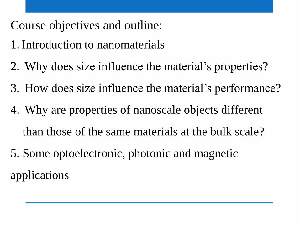
Course objectives and outline:
1. Introduction to nanomaterials
2. Why does size influence the material’s properties?
3. How does size influence the material’s performance?
4. Why are properties of nanoscale objects different
than those of the same materials at the bulk scale?
5. Some optoelectronic, photonic and magnetic
applications
3
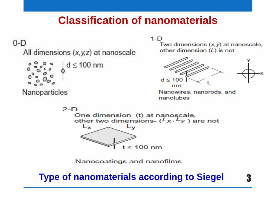
Classification of nanomaterials
Type of nanomaterials according to Siegel
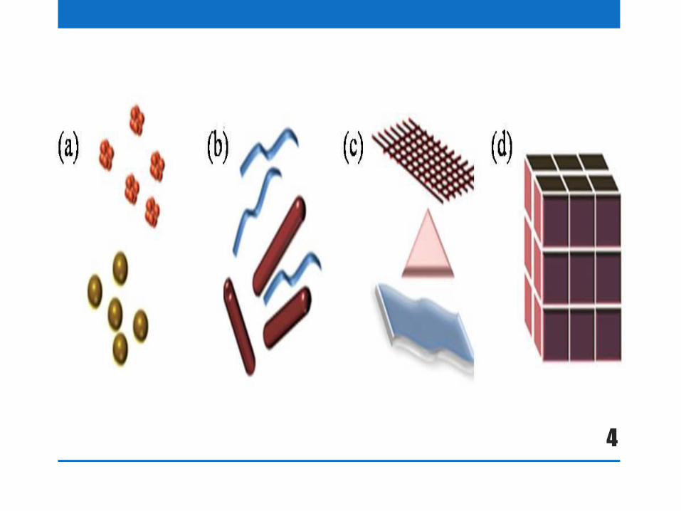
4
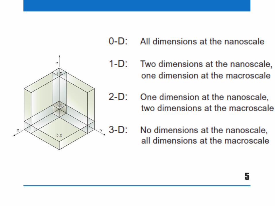
5
6
Number of papers on nanosciences published since their
discovery. Data is taken from Google Scholar
7
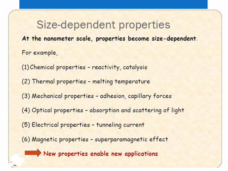
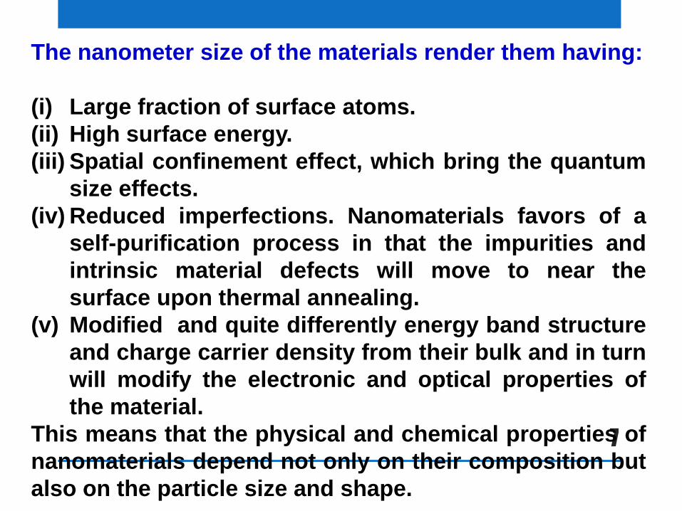
The nanometer size of the materials render them having:
(i) Large fraction of surface atoms.
(ii) High surface energy.
(iii) Spatial confinement effect, which bring the quantum
size effects.
(iv) Reduced imperfections. Nanomaterials favors of a
self-purification process in that the impurities and
intrinsic material defects will move to near the
surface upon thermal annealing.
(v) Modified and quite differently energy band structure
and charge carrier density from their bulk and in turn
will modify the electronic and optical properties of
the material.
This means that the physical and chemical properties of
nanomaterials depend not only on their composition but
also on the particle size and shape.
8
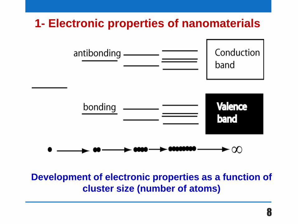
1- Electronic properties of nanomaterials
Development of electronic properties as a function of
cluster size (number of atoms)
9
• When several atoms are brought together into a
molecule, their atomic orbitals split and produces a
number of molecular orbitals proportional to the
number of atoms.
• In solids, there are so many atoms, the difference in
energy between them becomes very small, so that
forming bands of energy rather than the discrete
energy levels, that is to say form nearly continuous
bands of states.
• Each band has a width that reflects the interaction
between atoms, with a bandgap between the
conduction and the valence bands that reflects the
original separation of the bonding and antibonding
states.
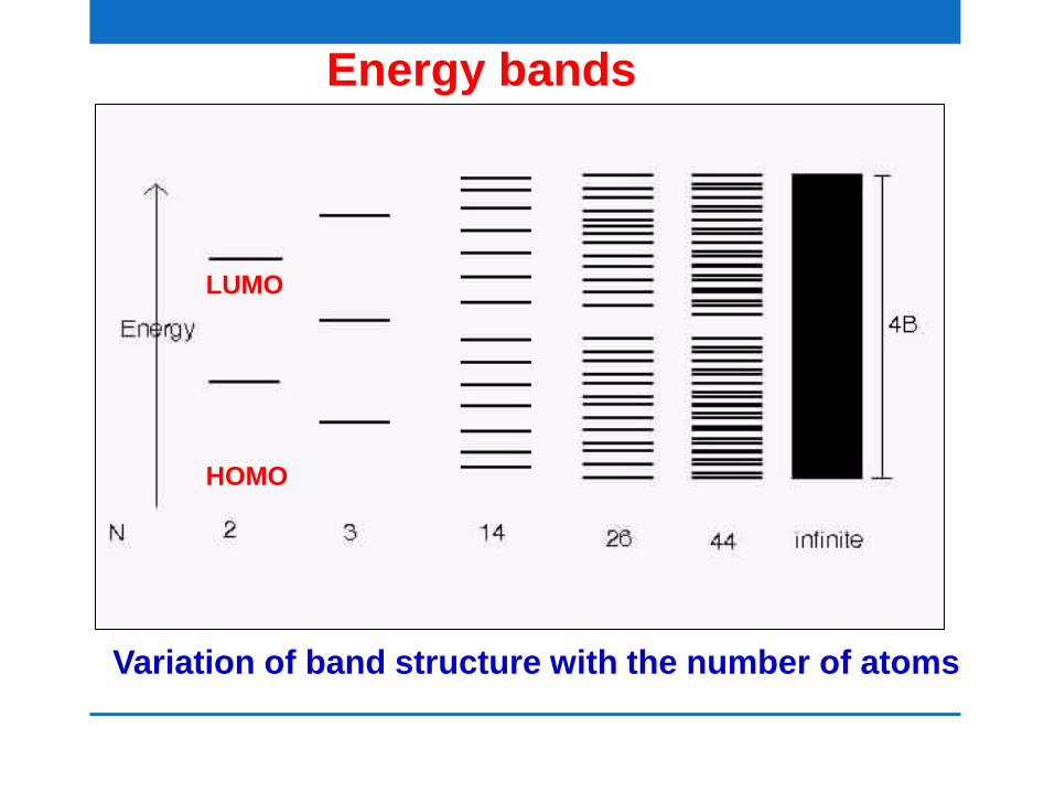
Energy bands
LUMO
HOMO
Variation of band structure with the number of atoms
11
1.1- Quantum confinement (size) effect
• Quantum Confinement is the spatial confinement of
electron-hole pairs (excitons) in one or more dimensions
within the material.
• This is due to changes in the atomic structure as a result of
ultra-small length scale on the energy band structure.
• Quantum confinement is more prominent in
semiconductors because they have an energy gap. Metals
do not have a bandgap.
• The regime of quantum confinement length scale ranges
from 2 to 25 nm for typical semiconductor groups of IV, III-
V and II-VI.
• These “geometrical” constraints, electrons “feel” the
presence of the particle boundaries and respond to
changes in particle size by adjusting their energy.
This phenomenon is known as the quantum-size effect.
12
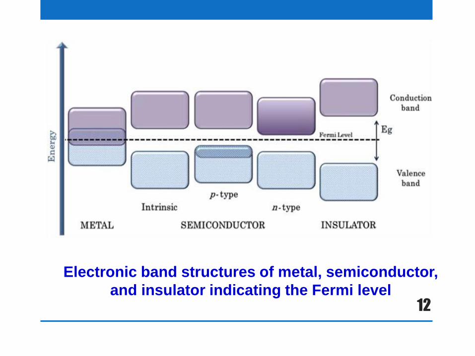
Electronic band structures of metal, semiconductor,
and insulator indicating the Fermi level
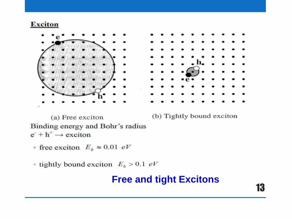
13 Free and tight Excitons
14
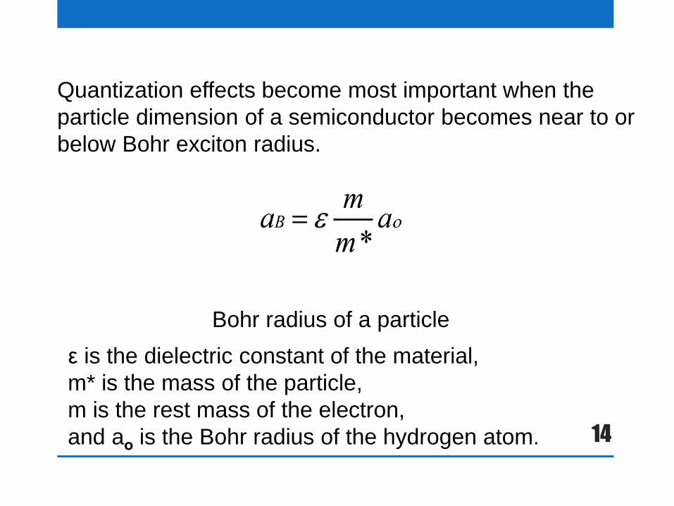
Quantization effects become most important when the
particle dimension of a semiconductor becomes near to or
below Bohr exciton radius.
Bohr radius of a particle
ε is the dielectric constant of the material,
m* is the mass of the particle,
m is the rest mass of the electron,
and aо is the Bohr radius of the hydrogen atom.
Quantum Confinement in Nanostructures
Electrons Confined in 1 Direction:
Quantum Wells (thin films):
Electrons can easily move in
2 Dimensions.
Electrons Confined in 2 Directions:
Quantum Wires:
Electrons can easily move in
1 Dimension.
Electrons Confined in 3 Directions:
Quantum Dots:
Electrons can easily move in
0 Dimensions.
kx
nz
ny
ny
nz
nx
kx
ky
nz 1 Dimensional
Quantization
2 Dimensional
Quantization
3 Dimensional
Quantization
16
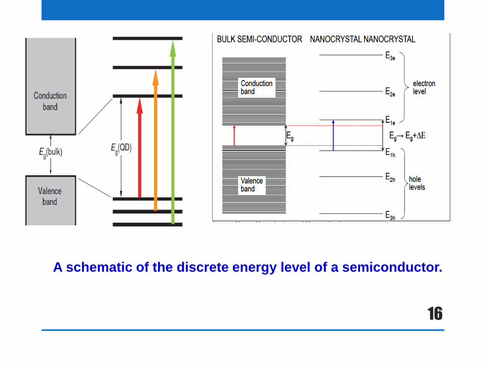
A schematic of the discrete energy level of a semiconductor.
17
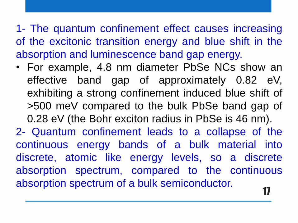
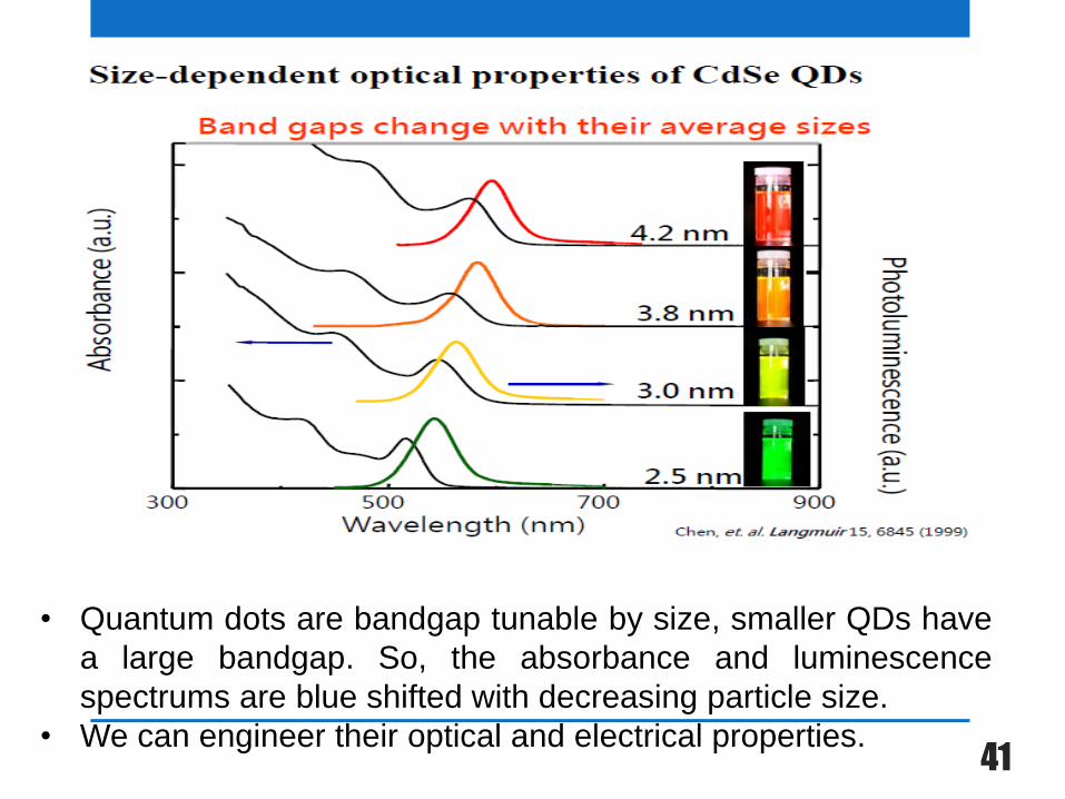
1- The quantum confinement effect causes increasing
of the excitonic transition energy and blue shift in the
absorption and luminescence band gap energy.
• For example, 4.8 nm diameter PbSe NCs show an
effective band gap of approximately 0.82 eV,
exhibiting a strong confinement induced blue shift of
>500 meV compared to the bulk PbSe band gap of
0.28 eV (the Bohr exciton radius in PbSe is 46 nm).
2- Quantum confinement leads to a collapse of the
continuous energy bands of a bulk material into
discrete, atomic like energy levels, so a discrete
absorption spectrum, compared to the continuous
absorption spectrum of a bulk semiconductor.
18
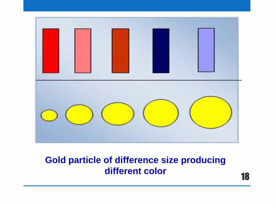
Gold particle of difference size producing
different color
19
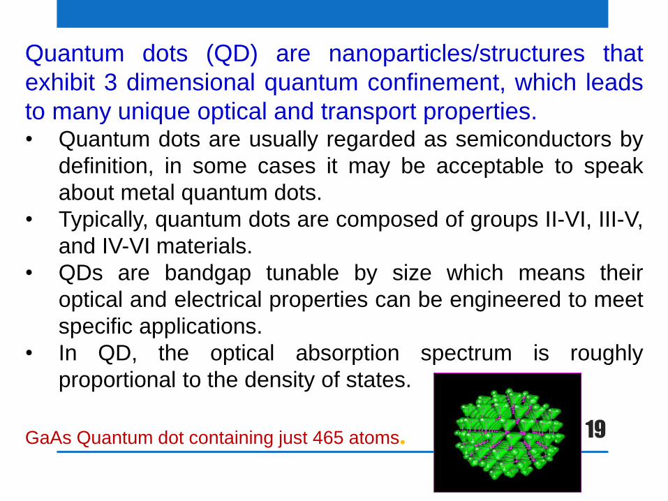
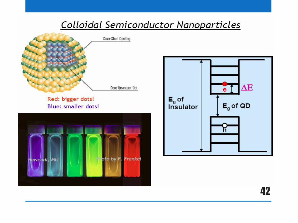
Quantum dots (QD) are nanoparticles/structures that
exhibit 3 dimensional quantum confinement, which leads
to many unique optical and transport properties. • Quantum dots are usually regarded as semiconductors by
definition, in some cases it may be acceptable to speak
about metal quantum dots.
• Typically, quantum dots are composed of groups II-VI, III-V,
and IV-VI materials.
• QDs are bandgap tunable by size which means their
optical and electrical properties can be engineered to meet
specific applications.
• In QD, the optical absorption spectrum is roughly
proportional to the density of states.
GaAs Quantum dot containing just 465 atoms.
20
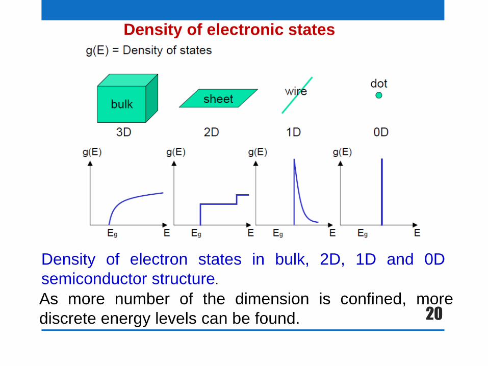
As more number of the dimension is confined, more
discrete energy levels can be found.
Density of electron states in bulk, 2D, 1D and 0D
semiconductor structure.
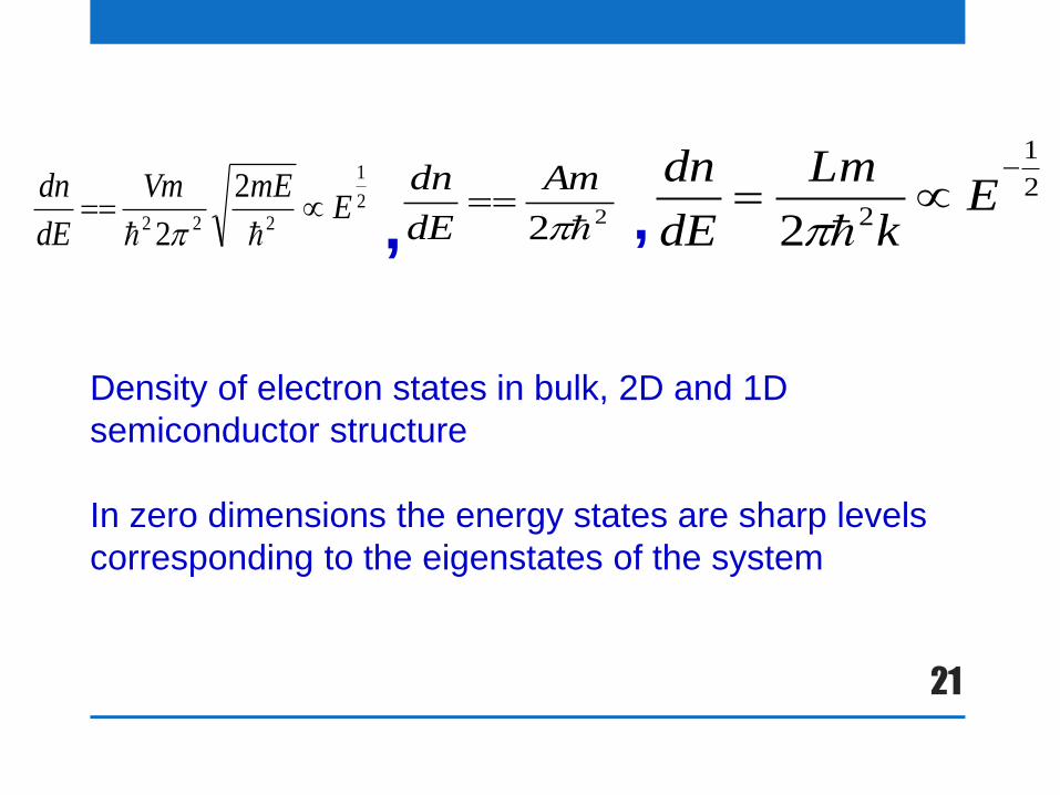
Density of electronic states
21
22
Am
dE
dn2
1
222
2
2E
mEVm
dE
dn
2
1
22
Ek
Lm
dE
dn
Density of electron states in bulk, 2D and 1D
semiconductor structure
In zero dimensions the energy states are sharp levels
corresponding to the eigenstates of the system
, ,
22
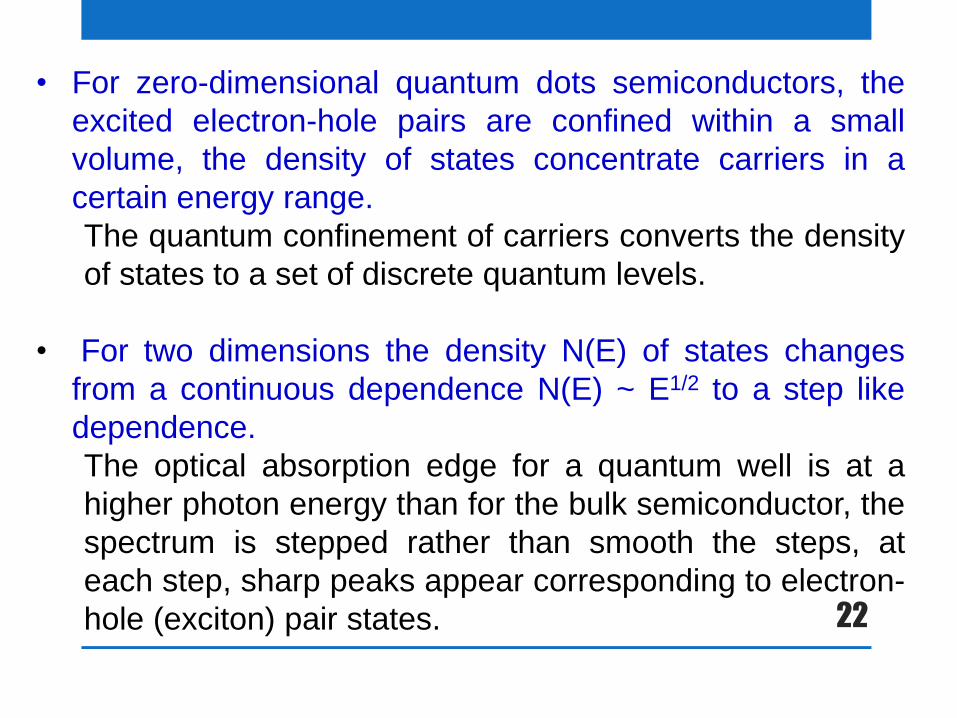
• For zero-dimensional quantum dots semiconductors, the
excited electron-hole pairs are confined within a small
volume, the density of states concentrate carriers in a
certain energy range.
The quantum confinement of carriers converts the density
of states to a set of discrete quantum levels.
• For two dimensions the density N(E) of states changes
from a continuous dependence N(E) ~ E1/2 to a step like
dependence.
The optical absorption edge for a quantum well is at a
higher photon energy than for the bulk semiconductor, the
spectrum is stepped rather than smooth the steps, at
each step, sharp peaks appear corresponding to electron-
hole (exciton) pair states.
23
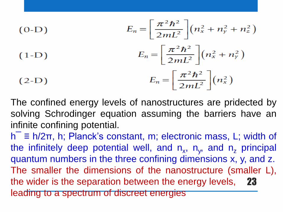
The confined energy levels of nanostructures are pridected by
solving Schrodinger equation assuming the barriers have an
infinite confining potential.
h¯ ≡ h/2π, h; Planck’s constant, m; electronic mass, L; width of
the infinitely deep potential well, and nx, ny, and nz principal
quantum numbers in the three confining dimensions x, y, and z.
The smaller the dimensions of the nanostructure (smaller L),
the wider is the separation between the energy levels,
leading to a spectrum of discreet energies
24
Weak confinement regime
• This regime is applicable to the case where the particle size
is small but still a few times larger than the exciton Bohr
diameter.
• The Coulomb energy is much larger than the confinement
energy resulting in the quantization of exciton center-of-
mass motion.
Strong confinement regime
• This regime is applicable to the case where the particle size
is much smaller than the exciton Bohr diameter.
• The Coulomb energy cannot be taken into consideration as
it is negligible with respect to confinement energy.
• The movement of both electron and hole is independent
and their confinements occur separately in the infinite
spherical potential.
25
1.2- Quantum well structures and its properties
• A quantum well (QW) is a particular kind of
heterostructure in which a single layer of material A
(layer thickness L), sandwiched between 2
macroscopically large layers of material B (usually, the
bandgaps satisfy: EgA < EgB).
• Both electrons and holes see lower energy in the "well"
layer, hence the name by analogy with a "potential well".
• The layer in which both electrons and holes are
confined, is so thin (typically about 100 Å or about 40
atomic layers) that we cannot neglect the fact that the
electron and hole are both waves.
• only particular waves are standing waves, the system is
quantized, hence the name "quantum well".
26
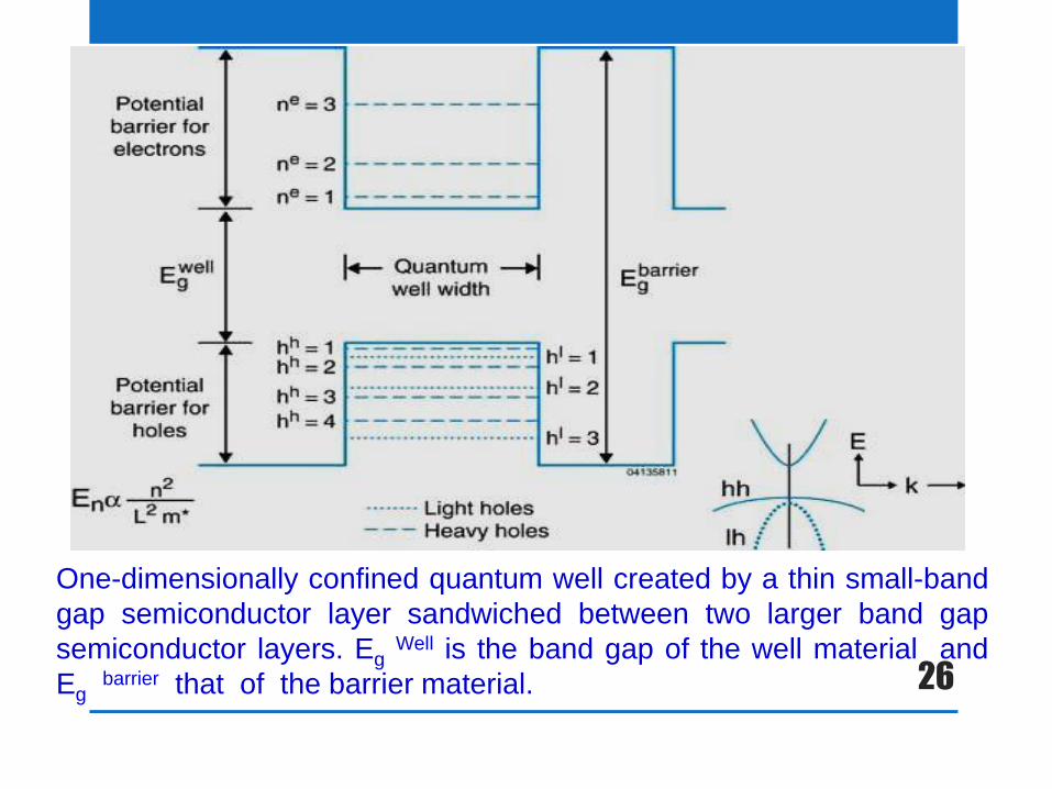
One-dimensionally confined quantum well created by a thin small-band
gap semiconductor layer sandwiched between two larger band gap
semiconductor layers. Eg Well is the band gap of the well material and
Eg barrier that of the barrier material.
27
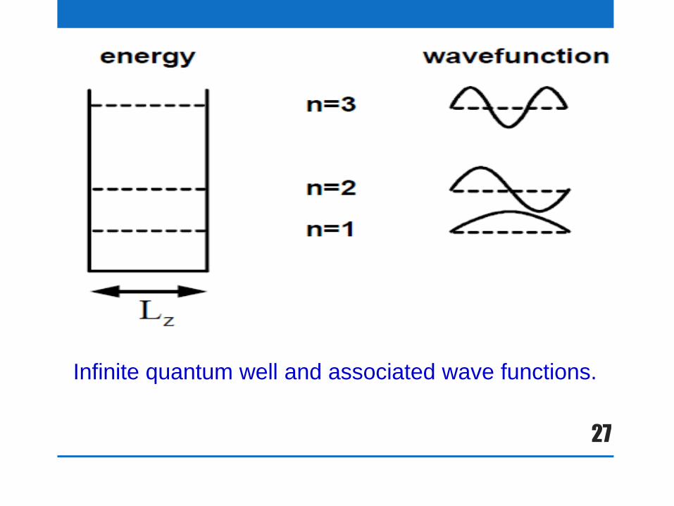
Infinite quantum well and associated wave functions.
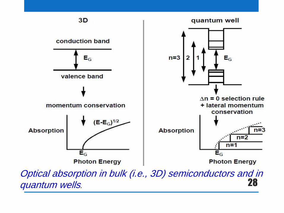
28 Optical absorption in bulk (i.e., 3D) semiconductors and in quantum wells.
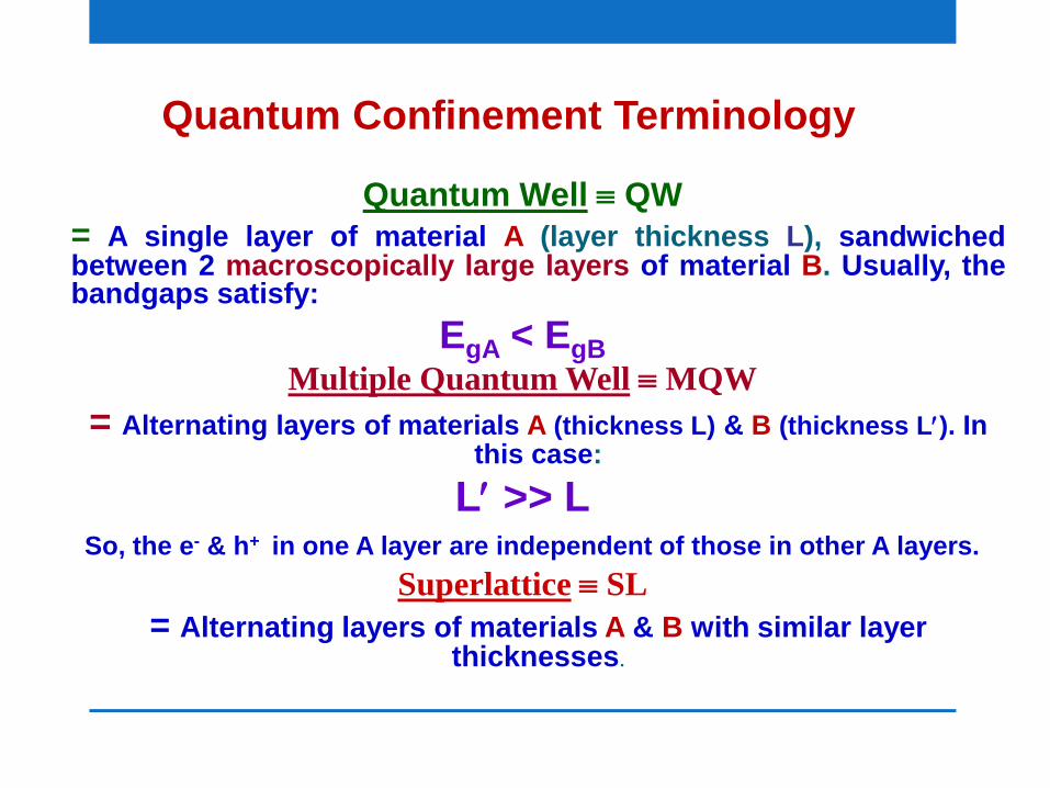
Quantum Well QW
= A single layer of material A (layer thickness L), sandwiched between 2 macroscopically large layers of material B. Usually, the bandgaps satisfy:
EgA < EgB
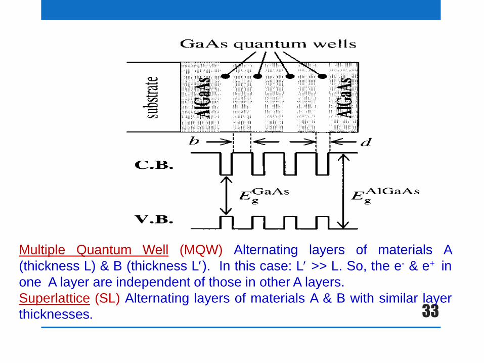
Multiple Quantum Well MQW
= Alternating layers of materials A (thickness L) & B (thickness L). In this case:
L >> L So, the e- & h+ in one A layer are independent of those in other A layers.
Superlattice SL
= Alternating layers of materials A & B with similar layer thicknesses.
Quantum Confinement Terminology
30
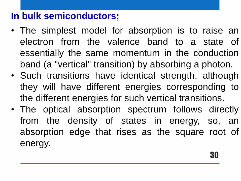
In bulk semiconductors;
• The simplest model for absorption is to raise an
electron from the valence band to a state of
essentially the same momentum in the conduction
band (a "vertical" transition) by absorbing a photon.
• Such transitions have identical strength, although
they will have different energies corresponding to
the different energies for such vertical transitions.
• The optical absorption spectrum follows directly
from the density of states in energy, so, an
absorption edge that rises as the square root of
energy.
31
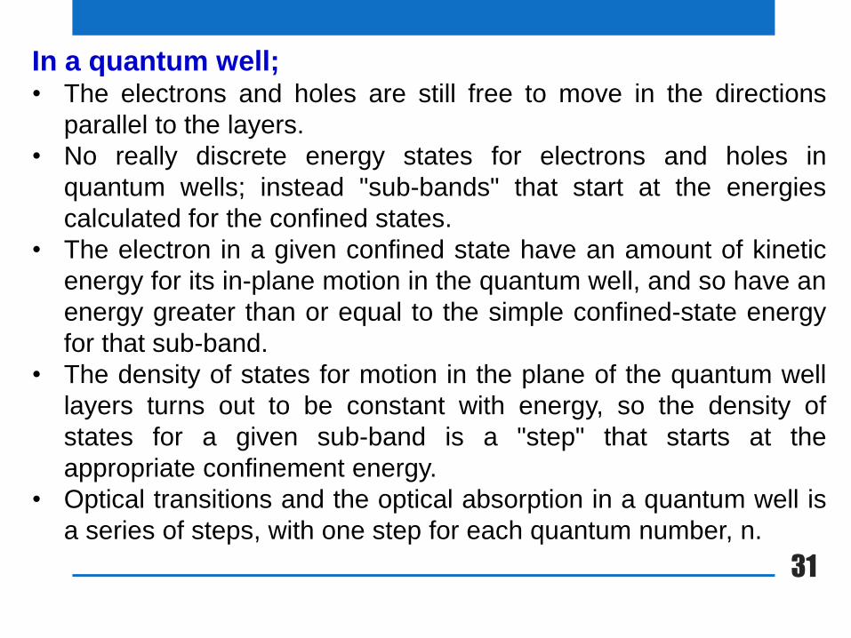
In a quantum well; • The electrons and holes are still free to move in the directions
parallel to the layers.
• No really discrete energy states for electrons and holes in
quantum wells; instead "sub-bands" that start at the energies
calculated for the confined states.
• The electron in a given confined state have an amount of kinetic
energy for its in-plane motion in the quantum well, and so have an
energy greater than or equal to the simple confined-state energy
for that sub-band.
• The density of states for motion in the plane of the quantum well
layers turns out to be constant with energy, so the density of
states for a given sub-band is a "step" that starts at the
appropriate confinement energy.
• Optical transitions and the optical absorption in a quantum well is
a series of steps, with one step for each quantum number, n.
32
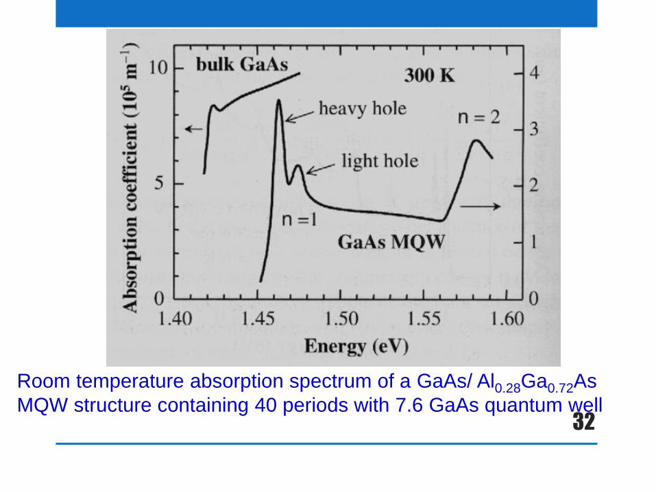
Room temperature absorption spectrum of a GaAs/ Al0.28Ga0.72As
MQW structure containing 40 periods with 7.6 GaAs quantum well
33
Multiple Quantum Well (MQW) Alternating layers of materials A
(thickness L) & B (thickness L). In this case: L >> L. So, the e- & e+ in
one A layer are independent of those in other A layers.
Superlattice (SL) Alternating layers of materials A & B with similar layer
thicknesses.
34
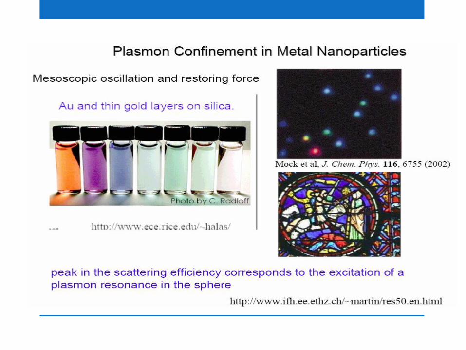
Surface Plasmons Resonance is;
• The oscillations of free electrons that are the consequence
of the formation of a dipole in the material due to
electromagnetic waves.
• The electrons migrate in the material to restore its initial
state, however, light in resonance causes the free-electrons
in the metal to oscillate. As the wave front of the light
passes, the electron density in the particle is polarized to
one surface and oscillates in resonance with the light’s
frequency causing a standing oscillation.
• This is referred to as the surface plasmon resonance, since
it is located at the surface.
2- Optical properties of nanomaterials
2.1- Origin of Surface Plasmon Resonance and
Coloring in Metal nanoparticles
35
<<
Nanoparticle
9
d
d
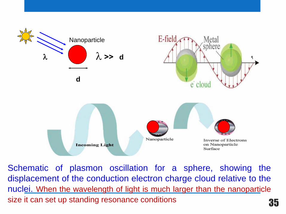
Schematic of plasmon oscillation for a sphere, showing the
displacement of the conduction electron charge cloud relative to the
nuclei. When the wavelength of light is much larger than the nanoparticle
size it can set up standing resonance conditions
36
• The resonance condition is determined from absorption
and scattering spectroscopy and is found to depend on the
shape, size, and dielectric constants of both the metal and
the surrounding material.
• As the shape or size of the nanoparticle changes, the
surface geometry changes, causing a shift in the electric
field density on the surface. This causes a change in the
oscillation frequency of the electrons, generating different
cross-sections for the optical properties including
absorption and scattering.
• The free electrons in the metal (d electrons in silver and
gold) are free to travel through the material. The mean free
path in gold and silver is ~50 nm, therefore in particles
smaller than this, no scattering is expected from the bulk.
37
The reduction of materials' dimension has
pronounced effects on the optical properties.
The size dependence can be generally
classified into two groups;
• One is due to the increased energy level
spacing as the system becomes more
confined,
• and the other is related to surface plasmon
resonance.
38
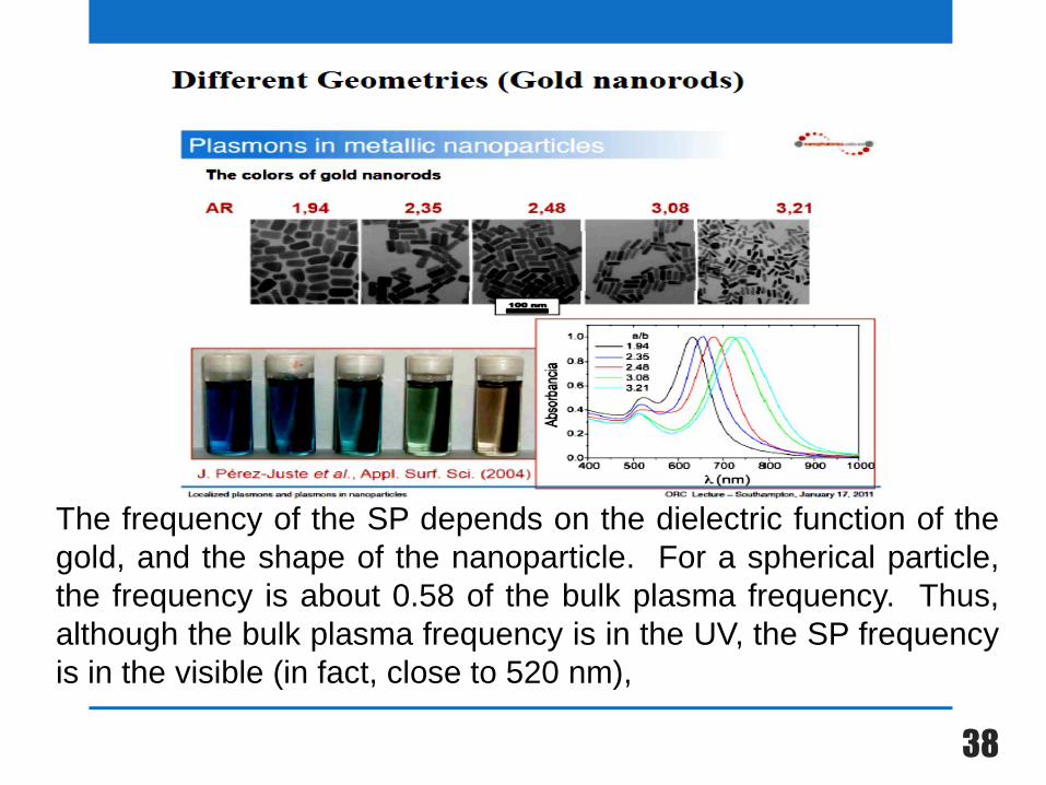
The frequency of the SP depends on the dielectric function of the
gold, and the shape of the nanoparticle. For a spherical particle,
the frequency is about 0.58 of the bulk plasma frequency. Thus,
although the bulk plasma frequency is in the UV, the SP frequency
is in the visible (in fact, close to 520 nm),
39
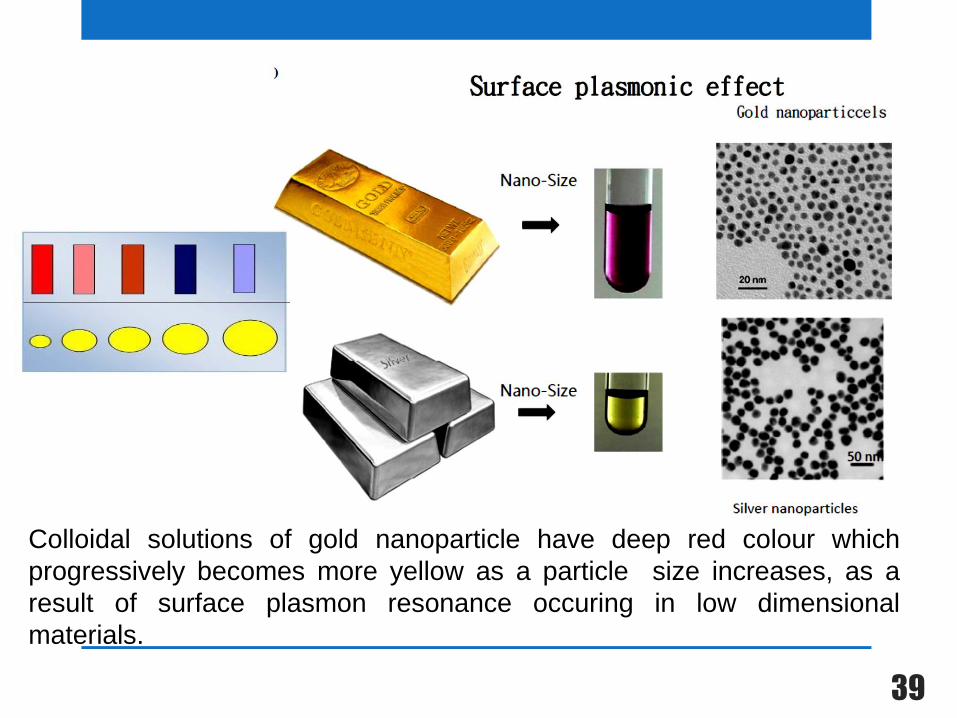
Colloidal solutions of gold nanoparticle have deep red colour which
progressively becomes more yellow as a particle size increases, as a
result of surface plasmon resonance occuring in low dimensional
materials.
40
41
• Quantum dots are bandgap tunable by size, smaller QDs have
a large bandgap. So, the absorbance and luminescence
spectrums are blue shifted with decreasing particle size.
• We can engineer their optical and electrical properties.
42
43


![Research Article Understanding the Formation of the Self ......Journal of Nanomaterials great interest because of the control of their optoelectronic properties[ ]. e growing interest](https://static.fdocuments.in/doc/165x107/601912c2d6c1ef375456df83/research-article-understanding-the-formation-of-the-self-journal-of-nanomaterials.jpg)