Sitronix ST7063C Controller Datasheet
12
ST Sitronix ST7063C 80CH Segment Driver for Dot Matrix LCD V1.3b 2005/11/08 1/12 n Functions l Dot matrix LCD driver with two 40 channel outputs l Bias voltage (V1 ~ V4) l input/output signals n Input : Serial display data and control pulse from controller IC n Output : 40 X 2 channels waveform for LCD driving n Features l Display driving bias : static to 1/5 l Power supply for logic : 2.7V ~ 5.5V l Power supply for LCD voltage (V DD ~V EE ) : 3V ~ 11V 100 Pin QFP package and bare chip available n Description ST7063C is a segment driver for dot matrix type LCD display. It features 80 channels with 40 X 2 bits bi-directional shift registers, data latches, LCD drivers and logic control circuits. It is fabricated by high voltage CMOS process with low current consumption. The ST7063C can convert serial data received from an LCD controller, such as ST7066U, into parallel data and send out LCD driving waveforms to the LCD panel. The ST7063C is designed for general purpose LCD drivers. It can drive both static and dynamic drive LCD. The LSI can be used as segment driver. The ST7063C has pin function compatibility with the KS0063(B) that allows the user to easily replace it with an ST7063C.
Transcript of Sitronix ST7063C Controller Datasheet
ST Sitronix ST7063C
80CH Segment Driver for Dot Matrix LCD
V1.3b 2005/11/08 1/12
n Functions
l Dot matrix LCD driver with two 40 channel
outputs
l Bias voltage (V1 ~ V4)
l input/output signals
n Input : Serial display data and control
pulse from controller IC
n Output : 40 X 2 channels waveform for
LCD driving
n Features
l Display driving bias : static to 1/5
l Power supply for logic : 2.7V ~ 5.5V
l Power supply for LCD voltage (VDD~VEE) :
3V ~ 11V
100 Pin QFP package and bare chip available
n Description
ST7063C is a segment driver for dot matrix type
LCD display. It features 80 channels with 40 X 2
bits bi-directional shift registers, data latches,
LCD drivers and logic control circuits. It is
fabricated by high voltage CMOS process with
low current consumption.
The ST7063C can convert serial data received
from an LCD controller, such as ST7066U, into
parallel data and send out LCD driving
waveforms to the LCD panel. The ST7063C is
designed for general purpose LCD drivers. It can
drive both static and dynamic drive LCD. The LSI
can be used as segment driver.
The ST7063C has pin function compatibility with
the KS0063(B) that allows the user to easily
replace it with an ST7063C.
ST7063C
V1.3b 2005/11/08 2/12
ST7063C Specification Revision History
Version Date Description
1.1 2000/07/31 First Edition
1.2 2000/11/14 Added QFP Pad Configuration(Page 6)
1.2a 2001/02/26 Changed Application Circuit(Page 11)
1.3 2001/05/04 1. ST7063 Transition to ST7063C 2. Moved QFP Package Dimensions Page 12 to Page 5
1.3a 2001/08/29 Added “Substrate connect to VDD”(Page 4)
1.3b 2005/11/08 Update temperature range

ST7063C
V1.3b 2005/11/08 3/12
n Functional Block Diagram
SEGMENT DRIVER SEGMENT DRIVER
BIDIRECTIONALSHIFTER(40bits)
BIDIRECTIONALSHIFTER(40bits)
DATA LATCH(40bits) DATA LATCH(40bits)
CONTOL
V1V2V3V4
CL2CL1M
DL1 SHL1 DR1 DL2 SHL2 DR2
VDD
VSS
VEE
S1...............................S40 S41...............................S80

ST7063C
V1.3b 2005/11/08 4/12
n Pad Arrangement
7877
7675
7473
7271
7069
6867
6665
6463
6261
6059
5857
5655
5453
5251
5049
95 94 93 92 91 90 89 88 87 86 85 84 83 82 81 80 7996
32 33 34 35 36 37 38 39 40 41 42 43 44 45 46 47 4831
12
34
56
78
910
1112
1314
1516
1718
1920
2122
2324
2526
2728
2930
Size : 3800x2600μ
m
Coordinate : center
Min. P
AD
Pitch : 120μ
m
PA
D S
ize : 90x90μm
(0,0)
Circle here to find the first P
AD
G793E
"G793E
" Marking : E
asy to find the PA
D
Substrate connect to VDD.

ST7063C
V1.3b 2005/11/08 5/12
n Package Dimensions
ST7063C
V1.3b 2005/11/08 6/12
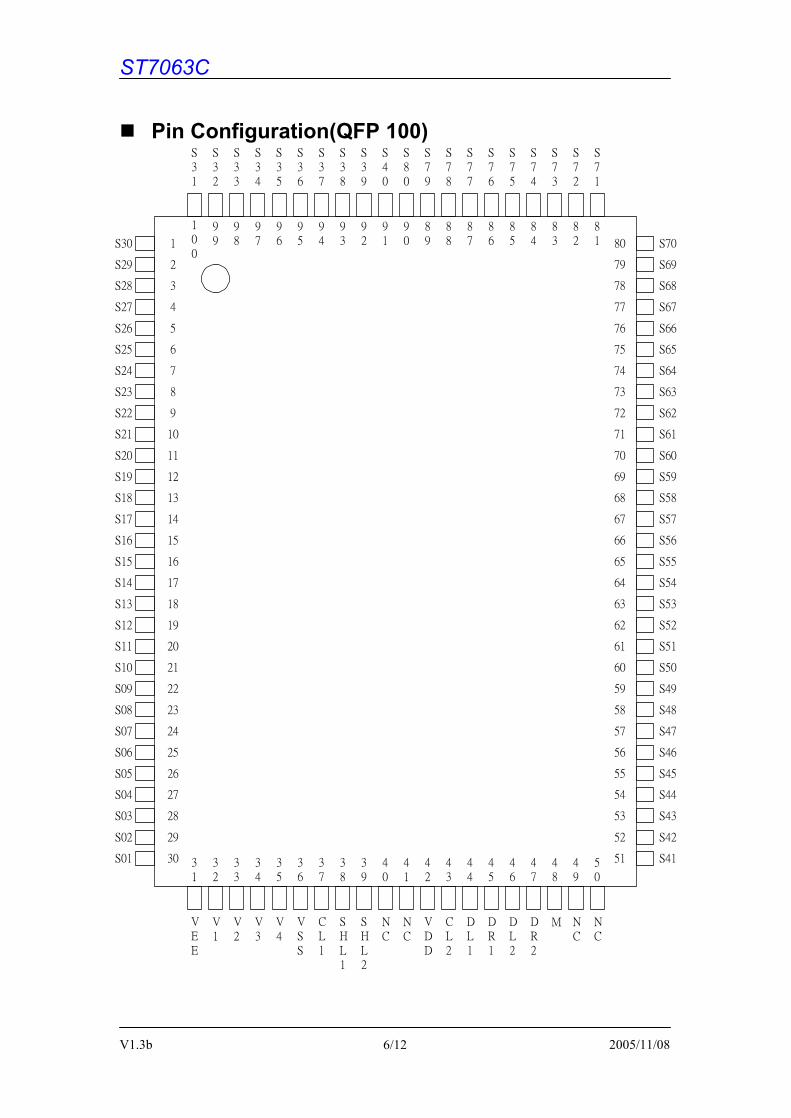
n Pin Configuration(QFP 100)
S30
S29
S28
S27
S26
S25
S24
S23
S22
S21
S20
S19
S18
S17
S16
S15
S14
S13
S12
S11
S10
S09
S08
S07
S06
S05
S04
S03
S02
S01
S70
S69
S68
S67
S66
S65
S64
S63
S62
S61
S60
S59
S58
S57
S56
S55
S54
S53
S52
S51
S50
S49
S48
S47
S46
S45
S44
S43
S42
S41
S31
S32
S33
S34
S35
S36
S37
S38
S39
S40
S80
S79
S78
S77
S76
S75
S74
S73
S72
S71
VEE
V1
V2
V3
V4
VSS
CL1
SHL1
SHL2
NC
NC
VDD
CL2
DL1
DR1
DL2
DR2
M NC
NC
1
2
3
4
5
6
7
8
9
10
11
12
13
14
15
16
17
18
19
20
21
22
23
24
25
26
27
28
29
30
80
79
78
77
76
75
74
73
72
71
70
69
68
67
66
65
64
63
62
61
60
59
58
57
56
55
54
53
52
51
100
99
98
97
96
95
94
93
92
91
90
89
88
86
85
84
83
82
81
87
31
32
33
34
35
36
37
38
39
40
41
42
43
45
46
47
48
49
50
44

ST7063C
V1.3b 2005/11/08 7/12
n Pad Name and Coordinates
Pad No. Pad Name X Y Pad No. Pad
Name X Y Pad No. Pad Name X Y
1 S42 -1760 -1160 33 S74 1760 -780 65 S15 -180 1160
2 S43 -1630 -1160 34 S75 1760 -660 66 S14 -300 1160
3 S44 -1500 -1160 35 S76 1760 -540 67 S13 -420 1160
4 S45 -1380 -1160 36 S77 1760 -420 68 S12 -540 1160
5 S46 -1260 -1160 37 S78 1760 -300 69 S11 -660 1160
6 S47 -1140 -1160 38 S79 1760 -180 70 S10 -780 1160
7 S48 -1020 -1160 39 S80 1760 -60 71 S9 -900 1160
8 S49 -900 -1160 40 S40 1760 60 72 S8 -1020 1160
9 S50 -780 -1160 41 S39 1760 180 73 S7 -1140 1160
10 S51 -660 -1160 42 S38 1760 300 74 S6 -1260 1160
11 S52 -540 -1160 43 S37 1760 420 75 S5 -1380 1160
12 S53 -420 -1160 44 S36 1760 540 76 S4 -1500 1160
13 S54 -300 -1160 45 S35 1760 660 77 S3 -1630 1160
14 S55 -180 -1160 46 S34 1760 780 78 S2 -1760 1160
15 S56 -60 -1160 47 S33 1760 900 79 S1 -1760 1030
16 S57 60 -1160 48 S32 1760 1030 80 VEE -1760 900
17 S58 180 -1160 49 S31 1760 1160 81 V1 -1760 780
18 S59 300 -1160 50 S30 1630 1160 82 V2 -1760 660
19 S60 420 -1160 51 S29 1500 1160 83 V3 -1760 540
20 S61 540 -1160 52 S28 1380 1160 84 V4 -1760 420
21 S62 660 -1160 53 S27 1260 1160 85 VSS -1760 300
22 S63 780 -1160 54 S26 1140 1160 86 CL1 -1760 180
23 S64 900 -1160 55 S25 1020 1160 87 SHL1 -1760 60
24 S65 1020 -1160 56 S24 900 1160 88 SHL2 -1760 -60
25 S66 1140 -1160 57 S23 780 1160 89 VDD -1760 -180
26 S67 1260 -1160 58 S22 660 1160 90 CL2 -1760 -300
27 S68 1380 -1160 59 S21 540 1160 91 DL1 -1760 -420
28 S69 1500 -1160 60 S20 420 1160 92 DR1 -1760 -540
29 S70 1630 -1160 61 S19 300 1160 93 DL2 -1760 -660
30 S71 1760 -1160 62 S18 180 1160 94 DR2 -1760 -780
31 S72 1760 -1030 63 S17 60 1160 95 M -1760 -900
32 S73 1760 -900 64 S16 -60 1160 96 S41 -1760 -1030

ST7063C
V1.3b 2005/11/08 8/12
n Pin Description
Pin Name Purpose Description I/O
VDD POWER for logic N/A
VSS GROUND for logic N/A
VEE LCD GND for LCD driving voltage N/A
V1 V2 LCD output used as select voltage level I
V3 V4 LCD output used as non select voltage level I
S1-S40 segment LCD driver output for part 1 O
SHL1 direction direction control for part 1 segments I
DL1, DR1 data in /out If SHL1 = 1 then DL1=out, DR1=in If SHL1 = 0 then DL1=in, DR1=out I/O
S41-S80 segment LCD driver output for part 2 O
SHL2 direction direction control for part 2 segments I
DL2, DR2 data in/out If SHL2 = 1 then DL2=out, DR2=in If SHL2 = 0 then DL2=in, DR2=out I/O
M alternation Alternate the LCD driving waveform I
CL1 latch clock latch the data after shift is completed I
CL2 shift clock shift the data into the segments I

ST7063C
V1.3b 2005/11/08 9/12
n Functional Description Clock
The CL1 is the clock to latch data on the falling edge. It latches the data input from
the bi-directional shift register at the falling edge of CL1 and transfers its outputs to
the LCD driver circuit. The CL2 is the clock to shift data on the falling edge. It shifts
the serial data at the falling of CL2 and transfers the output of each bit of the register
to the latch circuit.
Shift Registers And Data I/O
The ST7063C supplies two sets of 40-bit shift register, which controls the shift
direction by SHL1 & SHL2. The SHL1 controls the 1st 40-bit shift register, and SHL2
controls the 2nd 40-bit shift register. When SHL1 is connected to VDD, the 1st shift
direction is from S40 to S1; when SHL1 is connected to VSS, the shift direction
changes from S1 to S40. When SHL2 is connected to VDD, the 2nd shift direction is
from S80 to S41; when SHL2 is connected to VSS, the shift direction changes from
S41 to S80.
The DL1, DR1, DL2, DR2 are data input or output option function.
Shift Direction of Channel 1
SHL1 Shift Direction DL1 DR1
0 S1 à S40 IN OUT
1 S40 à S1 OUT IN
Shift Direction of Channel 2
SHL2 Shift Direction DL2 DR2
0 S41 à S80 IN OUT
1 S80 à S41 OUT IN

ST7063C
V1.3b 2005/11/08 10/12
n LCD Output Waveforms
n Timing Characteristics
Output of LATCH (DATA)
M
Output (S1 ~ S80)
V1 V1
V2
V3
V4
V2
V3
V4
CL2
Data in (DL1, DL2) (DR1, DR2)
Data out (DL1, DL2) (DR1, DR2)
CL1
M
VIH VIL
TR
TWCKH TF
TWCKL
TDH
TSU
TD
VOH VOL
TSL
TLS TLS
TWCKH
TR TSU

ST7063C
V1.3b 2005/11/08 11/12
n D.C Characteristics
Symbol Parameter Test Condition Min. Typ. Max. Unit Applicable pin
VDD Operating Voltage - 2.7 - 5.5 V -
VLCD Driver Supply Voltage VDD-VEE 3 - 11 V -
VIH Input High Voltage - 0.7 VDD - VDD V
VIL Input Low Voltage - 0 - 0.3 VDD V
ILKG Input Leakage Current VIN =0 ~ VDD -5 - 5 uA
CL1,CL2,M,SHL1,SHL2
DL1,DL2,DR1,DR2
VOH Output High Voltage IOH = -0.4mA VDD -0.4 - - V
VOL Output Low Voltage IOL = +0.4mA - - 0.4 V
DL1,DL2,DR1,DR2 V1~V4, S1~S80
IDD Operating Current FCL2 = 400KHZ - 100 300 uA VDD,VEE
IV Leakage Current VIN =VDD ~ VEE -10 - 10 uA V1 ~ V4
n A.C Characteristics
Symbol Parameter Test Condition Min. Max. Unit Applicable pin
FCL Data Shift Frequency - - 400 KHZ CL2
TWCKH Clock High Level Width - 800 - ns CL1,CL2
TWCKL Clock Low Level Width - 800 - ns CL2
TSL Clock Set-up Time CL2 à CL1 500 - ns CL1,CL2 TLS Clock Set-up Time CL1 à CL2 500 - ns CL1,CL2
TR/TF Clock Rise/Fall Time - - 200 ns CL1,CL2
TSU Data Set-up Time - 300 - ns DL1,DL2,DR1,DR2
TDH Data Hold Time - 300 - ns DL1,DL2,DR1,DR2
TD Data Delay Time CL = 15 PF - 500 ns DL1,DL2,DR1,DR2
n Maximum Absolute Ratings
Symbol Parameters Min. Max. Unit
VDD Supply Voltage -0.3 7 V
TOPR Operating Temperature -30 85 ℃
TSTG Storage Temperature -65 150 ℃

ST7063C
V1.3b 2005/11/08 12/12
n Application Circuit : (2Line x 40Word)
ST
7066U
ST
7063CS
T7063C
Dot M
atrix LC
D P
anel
-V or G
ND
Vcc(+
5V)
Regsister
Regsister
Regsister
Regsister
Regsister
VR
DB
0-DB
7
To M
PU
V5
V4
V3
V2
V1 M
CL
1
CL
2
GN
D
VC
C
Seg 1-40
Com
1-16
VE
E
VSS
SH
L2
SH
L1
VD
D
DL
1
V1
V2
V3
V4
V1
V2
V3
V4
VE
E
VSS
SH
L2
SH
L1
VD
D
DL
1
M
CL
2
CL
1
DR
1
DL
2
DR
2
M
CL
2
CL
1
DR
1
DL
2
DR
2Seg 1-80
Seg 1-80
Note:R
egsister=2.2K
~10K
ohm
VR
=10K
~30K
ohm
D