
Site control and optical characterization of InAs quantum …€¦ · · 2014-01-28Site control...
135
Site control and optical characterization of InAs quantum dots grown in GaAs nanoholes DISSERTATION zur Erlangung des Grades „Doktor der Naturwissenschafen“ an der Fakultät für Physik und Astronomie der Ruhr-Universität Bochum von Yu-Ying Hu aus New Taipei, Taiwan Bochum 2013
Transcript of Site control and optical characterization of InAs quantum …€¦ · · 2014-01-28Site control...

Site control and optical characterization of
InAs quantum dots grown in GaAs nanoholes
DISSERTATION
zur
Erlangung des Grades
„Doktor der Naturwissenschafen“
an der Fakultät für Physik und Astronomie
der Ruhr-Universität Bochum
von
Yu-Ying Hu
aus
New Taipei, Taiwan
Bochum 2013

1. Gutachter Prof. Dr. Andreas D. Wieck
2. Gutachter Prof. Dr. Ulrich Köhler
Datum der Disputation 19.11.2013


I
Contents
Contents ..................................................................................................................................... I
List of Abbreviations .............................................................................................................. III
List of Symbols........................................................................................................................ V
Chapter 1 Introduction ......................................................................................................... 1
Chapter 2 Semiconductor Quantum Dots ............................................................................ 5
2.1 Low-Dimensional Structures ..................................................................................... 5
2.2 Characterizations of Quantum Dots ........................................................................... 8
2.3 Energy Level Structure of Quantum Dots ................................................................ 10
Chapter 3 Epitaxial Growth of III-V Semiconductor Nanostructures ............................... 13
3.1 III-V Semiconductor Properties ............................................................................... 13
3.2 Growth Modes in Heteroepitaxy .............................................................................. 16
3.3 Molecular Beam Epitaxy System ............................................................................. 18
3.3.1 Solid source cells and shutters .......................................................................... 22
3.3.2 Substrate heating and manipulation .................................................................. 23
3.3.3 Growth parameters ............................................................................................ 23
3.3.4 Reflection high-energy electron diffraction ...................................................... 25
3.4 Self-Assembled 3D Nanostructures ......................................................................... 26
3.4.1 Strain-induced quantum dots (SK) ................................................................... 26
3.4.2 Nanostructures by droplet epitaxy (VW) .......................................................... 29
Chapter 4 Surface Patterning Techniques for Site-Selective Growth ............................... 33
4.1 Introduction to Site-Selective Growth ..................................................................... 33
4.2 Self-Assembled Nanohole Patterning ...................................................................... 36
4.3 Focused Ion Beam Patterning .................................................................................. 39
4.3.1 Equipment ......................................................................................................... 40
4.3.2 Process .............................................................................................................. 42
4.3.3 Patterning parameters ....................................................................................... 45

II
Chapter 5 Experimental Details and Characterization Methods ....................................... 49
5.1 Sample Fabrication ................................................................................................... 49
5.2 Scanning Electron Microscopy ................................................................................ 53
5.3 Atomic Force Microscopy ........................................................................................ 55
5.4 Photoluminescence Spectroscopy ............................................................................ 57
Chapter 6 Characterizations of Self-assembled/Self-patterned GaAs Nanoholes ............. 61
6.1 Randomly-distributed Nanoholes ............................................................................. 61
6.2 Arrayed Nanoholes ................................................................................................... 67
Chapter 7 Characterizations of Site-selected InAs Quantum Dots in GaAs Nanoholes ... 79
7.1 Topography .............................................................................................................. 79
7.1.1 Quantum dots in randomly-distributed nanoholes ............................................ 79
7.1.2 Quantum dots in arrayed nanoholes .................................................................. 84
7.2 Optical Properties of Quantum Dots in Randomly-distributed Nanoholes .............. 88
7.2.1 Quantum dot ensembles .................................................................................... 88
7.2.2 Single quantum dots .......................................................................................... 95
7.3 Optical properties of Quantum Dots in Arrayed Nanoholes .................................. 100
7.3.1 Quantum dot ensembles .................................................................................. 100
7.3.2 Single quantum dots ........................................................................................ 103
Chapter 8 Summary ......................................................................................................... 107
Bibliography ......................................................................................................................... 111
Appendix............................................................................................................................... 119
A.1 Index for Sample Number .......................................................................................... 119
A.2 Mask for Photolithography ........................................................................................ 120
A.3 Ion fluence for Planes and Lines ................................................................................ 121
Acknowledgements............................................................................................................... 123
Curriculum Vitae .................................................................................................................. 125

III
List of Abbreviations
1D, 2D and 3D One-, Two- and Three- Dimensional
2DEG Two-Dimensional Electron Gas
AFM Atomic Force Microscopy
BEP Beam Equivalent Pressure
BSE Backscattered Electron
CB Conduction Band
CL Cathodoluminescence
CVD Chemical Vapor Deposition
DE Droplet Epitaxy
DOS Density of States
EDX Energy Dispersive X-ray spectroscopy
FIB Focused Ion Beam
FM Frank-van der Merwe
FWHM Full Width at Half Maximum
IC Integrated Circuits
K-cell Knudsen effusion cell
LED Light Emitting Diode
LMIS Liquid Metal Ion Source
LPE Liquid Phase Epitaxy
MBE Molecular Beam Epitaxy
MEMS Micro-Electro-Mechanical System
ML Monolayer
MOCVD Metal-Organic Chemical Vapor Deposition
MOVPE Metal-Organic Vapor Phase Epitaxy
NH Nanohole
PBN Pyrolytic Boron Nitride
PL Photoluminescence
QD Quantum Dot
QDk Quantum Disk
QDM Quantum Dot Molecule
QR Quantum Ring
QW Quantum Well
QWR Quantum Wire

IV
RHEED Reflection High-Energy Electron Diffraction
SAQD Self-assembled Quantum Dot
SE Secondary Electron
SEM Scanning Electron Microscopy
SK Stranski-Krastanov
SNOM Scanning Near Field Optical Microscopy
SPM Scanning Probe Microscope
SRIM Stopping and Range of Ions in Matter
STM Scanning Tunneling Microscopy
TEM Transmission Electron Microscope
UHV Ultra-High Vacuum
VB Valence Band
VPE Vapor Phase Epitaxy
VW Volmer-Weber
WL Wetting Layer
AFP Lehrstuhl für Angewandte Festkörperphysik
MPI Max Planck Institute

V
List of Symbols
ao lattice constant
exciton Bohr radius
B magnetic field
C0 ion concentration
D ion dose
d thickness
E electrical field
e electron charge
E energy
Eg band gaps
ħ Dirac constant
h Planck’s constant
I ion beam current
J current density
k (kx, ky, kz) wave vector
kB Boltzmann’s constant
l, m, n quantum numbers
li width of facet
lspot spacing of FIB spots
Lx, Ly, Lz quantum confining dimensions
m*
effective mass
m0 free electron mass
p momentum
P vapor pressure
Q amount of deposited material
r (x, y) in-plane dimension
r radius
R⊥ perpendicular range
rn probability of single, double, or multiple nanoholes
Rp projected range
rsum occupancy rate of FIB spots by nanoholes
Tc congruent evaporation temperature
U voltage

VI
potential distribution
δ (x) Dirac function
ε eigen energy
εr permittivity
θ monolayer coverage
θ (x) Heaviside function
λdB de Broglie wavelength
μ chemical potential
µ*
reduced effective mass
ρ density
ρ(E) density of states
ρFIB nominal density of GaAs nanoholes
Φ ion fluence
φ lateral component of wavefunction Ψ
ψ vertical component of wavefunction Ψ
Ψ wavefunction
angular frequency

1
Chapter 1 Introduction
In semiconductor physics, low-dimensional heterostructures have been intensively studied in
the past decades, e.g. quantum wells (QW), quantum wires (QWR) and quantum dots (QD). The
major motivation for these studies originates from the quantum confinement effect in such low-
dimensional systems allowing the devices to represent interesting physical properties. Among
these low-dimensional heterostructures, QDs provide a complete three-dimensional (3D)
confinement for the charge carriers resulting in discrete densities of states which are in analogy
with atoms. Therefore, QDs are also known as “artificial atoms”. Due to their remarkable atom-
like properties, QDs are interesting to fundamental research and as well as applied technologies
[1, 2].
The tasks of QD studies and applications are mainly involved with the fabrication,
characterization and manipulation of the systems at a nanometer level. The common methods
for manufacturing semiconductor QDs are chemical synthesis [3, 4], lithography [5] and self-
assembly [6, 7]. The self-assembly method is carried out by an epitaxial growth, e.g., molecular
beam epitaxy (MBE), which has been considered as a promising technique to implement QDs
into atomic level semiconductor devices through a simple and effective process. For self-
assembled quantum dots (SAQD), InAs/GaAs system is one of the most widely studied material
systems due to its outstanding physical properties in points of preparations and applications. The
strain caused by the lattice mismatch between these two materials leads to the formation of 3D
islands, i.e., strain-induced QDs, over the surface of a 2D wetting layer on a substrate in a
Stranski-Krastanov (SK) growth mode [8–10]. Typically, strain-induced QDs have a defect-free
crystal quality, similar shapes, small sizes and narrow size-distributions. The line-up band gaps of
InAs and GaAs lead to a large potential well for both electrons and holes, which make the system
a good optical emitter with the wavelength in the near infrared range [11, 12]. Besides, the direct
band gap of InAs allows efficient optical transitions between the confined states of QDs [13].
Due to these advantages, InAs/GaAs SAQDs have become one of the most feasible objects for
exploring the fundamental physics and manipulating the applied devices of 3D quantum confined
systems.
With a conventional SK growth on a planar substrate, a great quantity of SAQDs can be
generated with a high density above the order of 1010
cm-2
which is required for the efficient
optoelectronic devices such as QD lasers, light emitting diodes (LED) and high performance

2
infrared photodetectors [14–16]. QD lasers using QDs as an active medium in the light emitting
region have the superior properties of lower threshold current and better temperature insensitivity
than bulk or QW lasers. Semiconductor QDs are also desirable for the novel quantum devices
used for transferring and processing information, i.e., quantum information processing. In
particular, single QDs and QD molecules have been considered as the potential candidates for the
implementation of single photon sources for quantum cryptography [17, 18] and the building
blocks for quantum computers, such as qubits and quantum gates [19, 20]. Using quantum-
mechanical phenomena, solid-state quantum computers which are scalable up to a large number
of qubits, are expected to comprehend massive data processing of special algorithmic calculations
with a higher resulting efficiency than digital computers [21]. However, with conventional strain-
induced QDs, the high density and random distribution make it difficult to address QDs
individually for the prospect single QD appliances. In addition, the size variety of strain-induced
QDs is restricted due to the self-limiting growth which narrows the range of the emission
wavelength for possible applications [22]. Therefore, the art of the site and size control with
SAQDs becomes one of the challenges for single QD researches.
Recently, an alternative self-assembly method with MBE has been developed, called droplet
epitaxy (DE). Droplet epitaxy is a two-steps growth method with the formation of metal droplets
by Volmer-Weber (VW) growth and the subsequent crystallization of the metal droplets [23].
Contrary to the approach of SK growth, DE provides a way with more flexibility in respect of
material systems, spatial densities and nanostructure configurations. For example, apart from
lattice-mismatched systems, lattice-matched systems are allowed with DE, e.g., GaAs/AlGaAs
for heteroepitaxy and GaAs/GaAs for homoepitaxy, because strains are not essential for VW
growth. Moreover, the densities can be altered from the order of 108 cm
-2 down to 10
6 cm
-2 which
are suitable for the study of single nanostructure spectroscopy. However, the crystal quality of
droplet epitaxy grown QDs is generally lower than that of SK grown QDs, which is affected by
the process of crystallization. In addition to QDs, various productions such as quantum rings
(QR), double quantum rings and nanoholes (NH) are also possible by DE [24–39]. Besides being
major studies, the ring-like structures and nanoholes formed by droplet epitaxy have been used
for nano-scale self-patterning in order to modulate the properties of overgrown nanostructures.
For example, they are useful to produce low-density QDs for single QD investigation by refilling
them with proper materials [40–46].
Owed to the progress of epitaxial growth techniques, the foundation of quantum hetero-
structure realization has been established in a more controllable and creative way. This thesis
presents a successful development combining the advantages of SK growth and droplet epitaxy to
fabricate high-quality InAs QDs inside low-density GaAs nanoholes via a site-selective growth
by MBE. With this development, GaAs nanoholes are self-patterned on GaAs (100) substrates by
droplet epitaxy, which can provide preferential nucleation sites for the overgrown InAs QDs
through a SK growth mode. The spatial distribution of the preferentially grown QDs, i.e., site-
selected QDs, is therefore determined by that of the nanoholes controlled by the formation of
metal droplets. This development provides an in-situ process to achieve a site-selective growth
3
without additional treatments since the SK growth for QDs and the droplet epitaxy for nanoholes
are fully compatible with MBE. Nevertheless, the locations of the site-selected QDs are randomly
distributed over the surface due to the nature of self-assembled nanoholes formed by droplet
epitaxy. In order to enhance the potential of the site-selected QDs grown in self-assembled
nanoholes for novel quantum devices which require QDs being integrated into intentional
positions, an artificial surface pre-patterning technique is commonly introduced. In this thesis, an
in-situ focused ion beam (FIB) patterning is used to overcome the random distribution of self-
assembled nanoholes into arbitrarily designed orders under an ultra-high vacuum (UHV)
environment. The FIB pre-patterning technique can locally modify a substrate surface so that
the overgrown nanostructures can be carried out in a site-controlled manner according to the
arrangement of designed patterns [47–50]. Therefore, positioned self-assembled nanoholes can be
produced by combining FIB pre-patterning and droplet epitaxy, which can be further used as
templates for the re-growth of QDs. Finally, with FIB-positioned GaAs nanoholes, the site-
control of InAs QDs can be obtained with a planned arrangement via a subsequent MBE growth.
The structure of this thesis after the present introduction is as follows. In chapter 2, the
fundamental background about semiconductor QDs is introduced. It starts with the theoretical
background and the physical properties of low-dimensional quantum confined structures. Then,
the important characteristics and different fabrication methods of semiconductor QDs are
described. A theoretical model used to deduce the energy level structure of self-assembled QDs is
also explained. Chapter 3 regarding the epitaxial growth begins with a brief overview of
the physical properties of III-V compound semiconductors which are commonly used for the
realization of low-dimensional systems. The typical crystal growth modes are described in the
second section including the general mechanisms and also that in practical cases of epitaxial
growth. Then, a description about the MBE system used in this work is addressed in detail.
Finally, the formation mechanisms of various self-assembled 3D nanostructures by two MBE
growth methods are described, especially in the cases of strain-induced InAs QDs and GaAs
nanoholes formed by droplet epitaxy. In chapter 4, the surface patterning techniques used for the
complementation of a site-selective growth are addressed. First, a literature survey about the site-
selective growth of SAQDs is described. Then, the particular approach to site-selected InAs QDs
applied in this work is introduced and explained, which is developed with self-patterned GaAs
nanoholes combining with or without FIB pre-patterning. A detailed description of the in-situ FIB
system and the patterning parameters used in this work are given in the last section of this chapter.
The details about sample fabrication and experimental characterization methods are opened and
described in chapter 5. The sample fabrication is provided with MBE growth, FIB pre-patterning
and sample processing. The structural characterizations are studied by scanning electron
microscopy (SEM) and atomic force microscopy (AFM), while the optical characterizations are
measured by photoluminescence (PL) spectroscopy and scanning near field optical microscopy
(SNOM). The experimental results and discussions are shown in chapter 6 and chapter 7. In
chapter 6, the results concerning the self-assembled/self-patterned GaAs nanoholes generated by
droplet epitaxy are reported along with the studies of their structures and distributions on a bare

4
GaAs surface (without FIB pre-patterning) and on a FIB-patterned GaAs surface. In the cases of
FIB pre-patterning, Ga+ and In
+ focused beams are applied to create square arrays of spots on a
nanometer scale prior to the fabrication of GaAs nanoholes. The influence of the FIB-patterning
parameters including ion fluence and spot spacing are studied experimentally to achieve the
optimum conditions for positioning the self-assembled nanoholes. On the other hand, the results
regarding the site-selected InAs QDs in the self-assembled GaAs nanoholes on a bare GaAs
surface and on a FIB-patterned GaAs surface are reported in chapter 7. This includes the growth
evolution of QDs with various amounts of InAs coverage and the influence of different FIB-
patterning parameters on the variation of sizes and densities. The optical properties of the QDs
are also addressed in this chapter for ensembles and single ones. In the end, a summary of the
results and concluding remarks of this work are given in chapter 8.

5
Chapter 2 Semiconductor Quantum Dots
The main purpose behind this work is to study the characteristics and the optical properties of the
semiconductor quantum dots (QDs). In this chapter, the general concepts related to QDs are
described. It starts with the theoretical background of quantum confinement in low-dimensional
semiconductor structures with respect to their physical properties. Then, the basic physical
properties and the fabrication methods of semiconductor quantum dots are addressed in particular.
In order to gain an insight of the optical properties, an adiabatic approximation employed to
deduce the energy level structure of the QDs is explained in the last section.
2.1 Low-Dimensional Structures
Charge carriers, i.e., electrons and holes, behave like free carriers in a bulk semiconductor
material where all three dimensions are much larger than the wavelength of their wavefunction,
i.e., de Broglie wavelength. If any of the dimensions is reduced to the order of the wavelength,
the charge carriers are squeezed with their motions confined in the corresponding direction
resulting in quantum confinement effect [51]. In general, the de Broglie wavelength of the charge
carriers is on the nanometer scale for semiconductors.
When quantum confinement is introduced in one, two or three dimensions, the energy band
structures and the density of states (DOS) of the charge carriers can deviate substantially from
that of a bulk semiconductor. As a result, the electronic and optical properties of the materials can
change dramatically. The carrier energy levels in semiconductors can be determined by solving
the Schrödinger equation in the effective mass approximation [52]:
* ħ
( )+Ψ ( ) Ψ ( ) .
where Ψ ( ) is the carrier wavefunction, * is the effective mass of the carrier, ħ is the Dirac
constant, ( ) is the potential distribution, and E is the energy of the system. Considering
the simple case of an infinitely deep, rectangular potential well, the Schrödinger equation can be
solved by the separation of variables method giving the confinement energies for one-, two- and
three- dimensional (1D, 2D and 3D) confinement.
In a bulk where there is no potential confinement for the carriers, i.e., 0D confinement, the
energy is quadratic in the wave vector ( ) as in the case of free particles:

6
u ħ
.
For 1D confinement, one dimension of the system, e.g., Lz, is strongly reduced. Therefore, the
carriers are confined in the direction z while they can move in a plane of (x, y). This kind of 1D
confinement can be realized by heterostructures in semiconductor called quantum wells (QW)
with the energy:
ħ
**
(
)
+ .
With 2D confinement, the system is confined along two directions, e.g., y and z, with the
dimensions of and as small as the de Broglie wavelengths. The carriers are allowed to move
only along one dimension of the structure which is known as a quantum wire (QWR). Its energy
has the form:
ħ
[
(
)
(
)
] .
In the case of 3D confinement, all three dimensions of , and are reduced so that there are
no free carries in the system. The carriers are confined to a box, called a quantum dot (QD). The
energy of a QD is written as:
ħ
[(
)
(
)
(
)
] .
In the above expressions of the energies, 1, 2, … are the quantum numbers. The
structures, QW, QWR and QD, are also known as 2D, 1D and 0D potential wells, respectively.
The corresponding density of states ρ( ) as a function of the energy is represented as
ρ u
( *)
⁄
ħ ⁄ .
ρ
ħ
∑ θ
( ) .
ρ
( )
⁄
∑( )
- ⁄
.
ρ
∑ δ
( ) .
where θ( ) is the Heaviside function with θ( ) as , and θ( ) as , and
δ( ) is the Dirac function.
With a decrease of the confining dimensional degree from 3D to 0D, the confinement
potential changes the density of states tremendously. According to the equations described above,
the density of states and the confinement energy of the electronic carriers can be plotted as
Figure 2.1 with respect to the confined and unconfined structures. The unconfined bulk material
has a continuous density of states in a proportion to √ . Quantum wells have a step-like density

7
of states. In quantum wires, the density of states has a relationship inversely proportional to √ .
Finally, quantum dots have discrete energy levels. These discrete energy levels can hold electrons
or holes of opposite spin direction following Pauli’s exclusion principle. These levels can be
filled sequentially starting from the lowest levels, i.e., the ground state, equivalently to the shell
filling in the orbitals of atoms [53]. Because of the analogies to the real atoms, the quantum dots
are often referred to as “artificia atoms” [1, 2]. However, the confinement potential of real atoms
is due to the Coulomb interaction between electrons and nucleus. Furthermore, the size of the
quantum dots is typically in the range of nanometers which is much larger than real atoms, e.g.,
0.53 Å for the Bohr radius of a hydrogen atom. Thus, the features of quantum dots in energy level
structures and optical properties are qualitatively different from those of atoms [54]. The
experimental results on different types of quantum dots revealed that the inter-subband energies
of QDs are of the order of several tens of meV. Compared to these value, the inter-subband
energies of atoms are three orders magnitude higher. Due to this fact, quantum dots are very
sensitive to temperature fluctuations, e.g., at room temperature kBT ≈ 26 meV. Therefore, we
need low temperatures to resolve the energy splitting of QDs.
Figure 2.1 The illustration for three-, two-, one-, and zero-dimensional
quantum confined structures and their corresponding densities of states ρ( ) as
a function of energy E. (courtesy of F. Tinjod [55])

8
2.2 Characterizations of Quantum Dots
As described in the previous section, a quantum dot is a nanostructure that confines the
motion of the charge carriers in all three spatial directions leading to discrete quantized energy
levels due to quantum confinement effects. The first experimental evidence and theoretical
description of 3D quantum confinement was published in the early 1980s with semiconductor
nanocrystals [56, 57]. The confinement in this case is formed by the presence of the interface
between different semiconductor materials. The semiconductor quantum dot is buried in another
semiconductor matrix while the band gap of the matrix material is larger than that of the quantum
dot material. Consequently, the electron energy level and the heavy-hole energy level are
quantized and lifted relative to the band edge of the bulk material [58]. Here, the heavy-hole
energy level is considered because it is the lowest level in the valence band in most common
semiconductors used for the realization of quantum dots. A quantum dot has electronic properties
intermediate between those of bulk materials and discrete molecules. The energy quantization of
both electrons and heavy holes depends on the size, shape and composition of QDs, as well as the
intrinsic properties of QD and matrix materials. In particular, the energy band gap of QDs is size-
dependent.
For an ideal quantum dot, the quantum confining dimensions Lx, Ly and Lz should be
comparable to the de Broglie wavelengths, λ , of carriers which depends on the effective mass
m* and temperature T following the relation of
λ
√ * .
where h is Planck’s constant and kB is Boltzmann’s constant. Comparing with the mass of a free
electron m0, the effective masses of electrons and holes in semiconductor materials are typically
smaller, e.g., a s* = 0.067 m0 and hh a s
* = 0.5 m0. As a result, the de Broglie wavelengths are
in the order of 10 nm to 100 nm for semiconductors at low temperatures. However, the de Broglie
wavelength is a soft criterion. The quantization effects are for example smeared out by thermal
broadening (~ kBT) resulting in fluctuations in the potential dimensions. If the thermal energy kBT
is smaller than the binding energy resulted from Coulomb attraction between the electron and the
hole confined in a QD, the bound electron-hole pair can be described as a quasi-particle, i.e., an
exciton. The spatial extension of an exciton is defined by the exciton Bohr radius, * .
*
ε
μ* .
where εr is the permittivity of the material, µ* is the reduced effective mass ( *⁄
*⁄
hh*⁄ ) and e is the electron charge of 1.602 × 10
-19 C. In typical semiconductor materials with
large εr and small µ*, the exciton Bohr radius is usually much larger than the hydrogen Bohr
radius and the lattice constant of the host material as well. Therefore, the corresponding
wavefunctions are spatially localized within the quantum dot, and extend over many periods of

9
the crystal lattice. Alternatively, the exciton Bohr radius is a convenient parameter to describe the
dimension of the QD instead of the de Broglie wavelength which has to be considered for
electrons and holes separately [58]. For example, the exciton Bohr radius for InAs is about 35 nm
[59]. Depending on the coupling degree between the electron and the hole in an exciton, there can
be strong or weak confinements which result in different energy state equations [60, 61].
There are many different ways to obtain 3D confinement, which results in different types of
semiconductor quantum dots. Here, three different types of QDs will be described in the
following. The first one is called colloidal quantum dots, which has been demonstrated since the
mid-1980s. Colloidal quantum dots are fabricated by chemical synthesis allowing manufactures
with large quantities and different sizes of quantum dots [3, 4]. Due to their special optical
properties, these quantum dots have been widely used as biological imaging tags [62] and also as
emitters in light emitting diodes (LED) [63]. The colloidal synthesis method is a low-cost and fast
technique to fabricate quantum dots. The second type of quantum dots is realized by lateral
electrostatic potential confinement of electrons in a two-dimensional electron gas (2DEG) or by
lateral lithographic patterning of a quantum well with vertical etching [5]. The method with
patterning has attracted much attention since the end of 1980s due to its many advantages. For
example, the quantum dots can be fabricated with various lateral shapes depending on the
resolution of lithographic techniques, e.g., photolithography, electron beam or focused ion beam
(FIB) lithography and scanning tunneling microscopy (STM). The etching techniques are reliable,
while some of them are easily available. Especially, it is compatible with large-scale modern
integrated semiconductor technology [1]. The fabrication for the third type of QDs is a self-
assembly process with a heteroepitaxial growth by molecular beam epitaxy (MBE) or metal-
organic chemical vapor deposition (MOCVD). This type of QDs is called self-assembled
quantum dots (SAQD) which are widely used in quantum research nowadays. With MBE,
SAQDs can be realized either in the Stranski-Krastanov (SK) growth mode or by droplet epitaxy
(DE) inherited by Volmer-Weber (VW) growth [6, 7]. In general, SAQDs have small and
uniform sizes and similar shapes. The size is usually a few tens of nanometers for the base
diameter and a few nanometers for the height, which can result in pronounced quantum size
effects. This method can easily integrate quantum dots into semiconductor heterostructures
without complicated and time-consuming patterning steps for QD devices, e.g., quantum dot
lasers with ensembles of QDs and single photon sources based on single QDs. For QD lasers, SK
grown QD ensembles have shown a good performance with high densities of the order from
109 to 10
11 cm
-2 [11, 14]. On the other hand, DE grown QDs representing low densities of the
order of 108 cm
-2 or lower, have become promising objects for single QD spectroscopy [17, 18].
Self-assembly also allows the generation of vertical quantum dot molecules (QDMs) by the
stacking of QD layers [5], or lateral QDMs by droplet epitaxy under specific growth conditions
[24]. Several heteroepitaxy material systems have been successfully employed, such as
InAs/GaAs, InAs/InP, InAlAs/AlGaAs, InP/GaAs, Ge/Si, GaN/AlGaN for strained systems and
GaAs/AlGaAs and GaAs/AlAs for un-strained systems [1, 7]. Among them, the most studied one

10
is InAs/GaAs system which is also used in this work. More details related to InAs/GaAs QDs will
be described in the next chapter.
2.3 Energy Level Structure of Quantum Dots
An artificial atom, i.e., a quantum dot, contains a finite number of conduction band electrons
and valence band holes or excitons of the order of 1 to 100, which means a finite number of
elementary electric charges. Because of this fact, the properties of quantum dots will be changed
even with the addition or removal of only one single electron. Small quantum dots like colloidal
semiconductor nanocrystals can be as small as 2 nm to 10 nm which corresponds to 10 to
50 atoms in diameter and a total number of 100 to 100,000 atoms within the volume of a QD. For
self-assembled quantum dots, the size is typically between 10 nm and 100 nm corresponding to
approximately 1,000 to 1,000,000 lattice atoms [64].
In order to study the properties of the quantum dots composed of a certain amount of atoms,
different theoretical models have been used to deduce their energy level structure [65, 66]. The
simplest model used to realize the energy eigenstates in a quantum dot is the calculation of a
particle in a sphere potential considering the case of an infinite barrier and a finite barrier with
different inner and outer materials (different masses). This model is mostly sufficient for a large
class of dots with the shape close to a spherical form [67]. However, depending on different
growth methods and parameters, QDs with different shapes have been reported, such as lens
shape [10], facets [68] and pyramidal shape [6]. For those QDs with the shapes different from
spherical, the potential is not separable and the Schrödinger equation has to be solved
numerically in most of the cases. However, there is a semi-classical approach including the
effective mass approximation which has been applied for such QD systems [66, 69]. In this work,
the lens-shaped dots are studied which are usually considered in self-assembled quantum dots.
Lens-shaped dots were first reported by D. Leonard et al., which are described as a part of a
sphere with a given base and a height with the ratio of 1/2 to the base diameter [10, 70]. Based on
the geometry, it is suggested that the carrier confinement in the growth-direction (vertical-,
z-direction) is stronger than that in the lateral directions (in-plane-, x, y-direction). In an adiabatic
approximation, the single particle wavefunction was derived in the envelope function formalism
by effective mass approximation [71]. With this approximation, the vertical ψ( ) component of
the wavefunction can be separated from the lateral φ( ) one. Therefore, the wavefunction can
be represented as
Ψ( ) φ( ) ψ( ) φ( ) ψ( ) .
which obeys the following time-independent 3D Schrödinger wave equation:
[ ( )
]Ψ Ψ , wh r ( ) .
The potential ( ) can be decomposed into two parts:
( ) ( ) ( ) .

11
where ( ) corresponds to the potential at the center of the dot with respect to x-y plane and
is the potential difference.
Due to the strong confinement in vertical direction for lens-shaped quantum dots, the vertical
component ψ( ) can be approximated by ψ ( ) of the 1D Schrödinger wave equation at the
lateral center, :
[ ( )
] ψ ( ) ε
ψ ( ) .
Because higher excited states (n > 0) are only weakly bound and their eigen energies are larger
compared with the observed quantum dot states, the mixing of such states is not taken into
account. Within the adiabatic approximation, the ground state energy ε can be identified with the
undisturbed sub-band edge while the perturbation is constituted by the potential difference of
( ).
A 2D Schrödinger wave equation for the lateral component φ( ) can be obtained by
inserting equations 2.12, 2.14 and 2.15 into 2.13:
[⟨ψ | |ψ
⟩
] φ ( ) ( ε
) φ ( ) .
The “undisturbed sub-band edge” ε can be considered as the “zero energy” for these states. The
integral term ⟨ψ | |ψ
⟩ can be referred to as a lateral effective potential, ( ):
( ) ⟨ψ | |ψ
⟩ ∫ψ
( ) ψ
*( , ) ( , ) .
In a semiclassical approach, this potential ( ) describes the lateral modulation of sub-band
edges. Applying an adiabatic approximation, the local sub-band edge ε ( ) depending on the
lateral position (the ground state eigen energy value of the 1D Schrödinger wave equation solved
at position r = (x,y)) can be assumed as a lateral effective potential:
( ) ε ( ) .
A scheme representing the adiabatic approximation for electrons in a lens-shaped dot is
shown in Figure 2.2. In this case, the xy-dependent ground state energy with respect to the
z-quantization determines the lateral confinement potential. For such a confinement, the 2D
harmonic oscillator potential is a good approximation as the example of a particle with the
effective mass of * bound laterally in a quantum well (in x-y plane) by a parabolic potential of
( )
( ) .
The quantum level energies can then be approximated by the simple formula:
ħ ( ) .
where is the angular frequency. ħ is represented as the lateral confinement energy. n and l
are the quantum numbers corresponding to the eigenstates of a 2D harmonic oscillator [72]. In
analogy to atomic physics, the energy levels of a QD with their quantum number adding up to
2n + l = 0, 1, 2…. correspond to the s, p, d shells, respectively. On the other hand, the vertical

12
potential ( ) can also be considered as a 1D-harmonic oscillator potential used for describing
the structure of spherical quantum dots [73]:
( )
*
.
The quantum energy levels of a 1D-harmonic oscillator potential can be represented as:
ħ (
) .
where and n are the angular frequency and the quantum number corresponding to the 1D
harmonic oscillator, respectively. ħ is represented as the vertical confinement energy. However,
the observable level structure of lens-shaped QDs is mainly determined by the in-plane
confinement [53]. The energy eigen states for a 3D lens-shaped quantum dot has been computed
by A. Wojs et al. [69]. With a finite potential barrier in an effective mass approximation, the
resulting particle for such dots resembles well to the case of a 2D harmonic oscillator.
The above approach shows the characteristic quantization of the energy levels resulting from
the lateral confinement, and also the dependency of these energy levels on the effective mass of
carriers and the size of dots. In other words, the properties of quantum dots can be controlled by
changing the size and/or the shape of the fabricated potential [74]. Many experimental electronic
and optical properties of self-assembled InAs quantum dots had been explained based on the
theoretical model of 2D harmonic oscillators [75, 76]. The detailed knowledge of the energy level
structure helps for determining the physical properties of quantum dots, which is very interesting
from a fundamental point of view as well as to possible applications. However, it is important to
note that the approach considers only single quantum dots. For QD ensembles containing dots
with various radii, the size distribution has to be considered. The optical resonance energies
strongly depend on the radius of QDs. This leads to a resonance distribution which manifests
itself as an inhomogeneous broadening in optical spectra [77].
Figure 2.2 Schematic illustration of the adiabatic approximation for electrons in a lens-
shaped quantum dot. Assuming that the vertical confinement (along z) is so strong that only
the ground state is occupied, the ground state energy can be assumed as the lateral effective
potential resulting in the lateral confinement of the quantum dot being parabolic. The
widths of the potential wells of vertical confinement are the same with the heights of the
quantum dot, z1, z2 and z3, with respect to the position of (x,y).

13
Chapter 3 Epitaxial Growth of III-V Semiconductor
Nanostructures
Owed to the development of molecular beam epitaxy in the 1970s, the quantized properties of
low-dimensional nanostructures have been largely investigated and manipulated. This chapter
begins with an introduction of III-V compound semiconductors which are widely used for the
realization of such quantum confined structures due to their unique properties. These properties
determine the electric and optical properties of the semiconductor devices as well as whether
an epitaxial growth is allowed with the materials. Three different crystal growth modes are
introduced in the second section, including the general mechanisms and also those in the practical
cases of epitaxy. The molecular beam epitaxy system used in this work and its working principle
are described in the third section. In the end, two different MBE growth methods for 3D self-
assembled nanostructures are introduced and described in detail.
3.1 III-V Semiconductor Properties
It has been proposed in the beginning of the 1950s that the semiconducting properties of
III-V compounds are obtained by combining group III elements, essentially Al, Ga and In, with
group V elements, essentially N, P, As and Sb, in the periodic table [78]. These III-V compound
semiconductors crystallize either in a zinc-blende lattice structure (GaAs, AlAs, InAs, GaSb,
InSb, GaP and InP) or in a wurtzite lattice structure (GaN, AlN and InN). A zinc-blende structure
is made up of two interpenetrating face centered cubic sub-lattices, while a wurtzite structure is
based on hexagonal lattices. Both of them have partly ionic and covalent bonding characters [79].
In the following, the properties of zinc-blende III-V compound semiconductors will be stressed,
especially GaAs and InAs, which are the materials used for the quantum dot structures in this
work. A scheme of the zinc-blende lattice structure is shown in Figure 3.1(a).
One of the most important properties of III-V compound semiconductors is the energy band
gap Eg, an energy interval without allowed states for the charge carriers. It is defined as the
smallest energetic distance between the top of the valence band and the bottom of the conduction
band. Figure 3.1 (b) shows a simplified band diagram for GaAs or InAs. The minimum of
the conduction band and the maximum of the valence band are both at the Γ-point (k = 0)
in reciprocal space. Semiconductors with this feature are referred to as direct bandgap

14
semiconductors. A direct band gap is essential for optical applications like light emitting diodes
(LED), because the exciton, i.e., the electron-hole pair can recombine to emit a photon directly
without requiring phonon interaction to ensure momentum conservation. It makes the generation
of light faster and more effective, since only then electrons and holes meet simultaneously in real
and in momentum space in the same moment. In this context, the recombination wavelength
defined by the band gap is an important property for specific applications. For example, in the
case of telecommunication applications, the commonly used wavelength of 1.55 µm is highly
desired because the losses of optical glass fibers are minimal at this wavelength. The most
commonly used III-V semiconductors have a direct band gap, e.g., GaAs, InAs, GaN and InP.
The band gap is often plotted versus the lattice constant ao as shown in Figure 3.2 because these
two are the most important parameters to determine the optoelectronic properties and the
fabrication processes of these III-V compound semiconductor devices. Both band gap energies
and lattice constants are temperature dependent. The lattice constant increases with increasing
temperature due to inharmonicity of the binding potential, while the band gap decreases because
of the atomic vibrations. The relations of temperature dependence for GaAs and InAs are listed in
Table 3.1. At 300 K, the direct band gaps are Eg,GaAs = 1.42 eV and Eg,InAs = 0.35 eV, and the
lattice constants are ao,GaAs = 5.6533 Å and ao,InAs = 6.0583 Å for GaAs and InAs, respectively.
III-V semiconductors can completely dissolve into each other. Therefore, the lines in
Figure 3.2 connecting the circles of specific binary compounds represent the energy band gaps
and lattice constants for ternary alloys depending on the mole fractions of the materials, e.g.,
AlxGa1-xAs, with x ranging continuously from 0 to 1. Furthermore, quaternary alloys are also
possible, e.g., GaxIn1-xAsyP1-y, with x and y ranging continuously from 0 to 1. Due to this fact, it
is possible to tailor the properties of the compounds for the desired applications by choosing
different elements and their compositions in a certain arbitrary ratio. This technique is referred to
as band gap engineering or band gap tailoring which makes III-V compound semiconductors
technically more flexible than elemental semiconductors like Si or Ge. Nowadays, a wide range
of bulk III-V compound semiconductors like GaAs and AlxGa1-xAs is used for traditional
semiconductor devices like transistors and lasers. However, due to the advances of epitaxial
techniques such as MBE [80, 81], liquid phase epitaxy (LPE) [82], metal-organic vapor phase
epitaxy (MOVPE) [83] and chemical vapor deposition (CVD) [84], III-V compound
semiconductors are being employed in new science and technology fields in the recent decades.
In other words, III-V compound semiconductors can be carried out not only for novel
optoelectronic devices with layered structures of different materials, but also for fundamental
investigation of low-dimensional solid-state nanostructures. More details about the epitaxial
techniques and the growth methods will be discussed in the next sections.
15
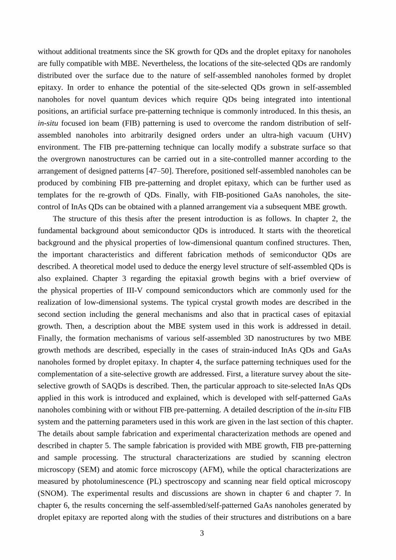
Temperature
dependency GaAs InAs
lattice constant
ao (Å) ao = 5.65325 + 3.88×10
-5·(T - 300) ao = 6.0583 + 2.74×10
-5·(T - 300)
direct band gap
Eg(Γ) (eV)
Eg = 1.519 - 5.405×10⁻⁴
·T 2
/ ( T + 204 )
(0 < T (K) < 103)
Eg = 0.415 - 2.76×10⁻⁴
·T 2
/ ( T + 83 )
(0 < T (K) < 300)
Table 3.1 Temperature dependences for the lattice constants and direct band gaps of GaAs and
InAs [13, 85].
(a) (b)
Figure 3.1 (a) The zinc-blende structure of the III-V compound semiconductor, GaAs. Dark
spheres correspond to Ga atoms. Light spheres correspond to As atoms. The lattice constant ao is
defined by the edge length of the cube. (b) The band structure of GaAs or InAs with a direct band
gap Eg at the Γ-point with k = 0. At 300 K, the band gaps are 1.42 eV for GaAs and 0.35 eV for
InAs, respectively [86].
Figure 3.2 Band gap energy versus lattice constant for zinc-blende III-V
compound semiconductors at room temperature. (courtesy of P. Tien [87])

16
3.2 Growth Modes in Heteroepitaxy
Th wor “ pitaxy” consists of two Greek words, “έπι” (epi) and “τάξ” (taxis), which mean
“on” an “arrang m nt”, r sp ctiv y. Epitaxial growth refers to a crystalline layer arranged on a
crystalline substrate in a way that one or more preferred orientations of the layer are aligned with
respect to the substrate. These kind of well-ordered layers are called epitaxial layers or epitaxial
films. In epitaxy, there are two different types of growth depending on the material systems. One
is homoepitaxy, where the substrate and the deposited materials are the same, e.g., the deposition
of Si on Si substrates or GaAs on GaAs substrates, which can be used to produce a highly pure
epitaxial layer based on the substrate. The other one is heteroepitaxy, where different materials
are deposited on the substrate, e.g., AlAs on GaAs substrates, which allows the fabrication of
heterostructures like quantum wells, quantum wires and quantum dots with the technique of band
structure engineering [88].
Generally, there are three crystal growth modes as shown in the schematic illustration of
Figure 3.3. The first one, (1) Frank-van der Merwe (FM) growth, is also called layer by layer
growth where adatoms are more strongly bound to the substrate than to each other. The adatoms
initially condense to form a complete monolayer on the substrate. The first layer is then covered
by the second layer which is a little less tightly bound. This kind of mode is observed in some
metal on metal systems, and also in semiconductor on semiconductor systems, e.g., GaAs on
GaAs or AlxGa1-xAs on GaAs. The second, (2) Volmer-Weber (VW) growth, is also named island
growth where adatom-adatom interactions are stronger than those of adatom-substrate. Therefore,
the adatoms are preferentially bound to each other rather than to the substrate, leading to the
formation of three-dimensional clusters [89]. These clusters which are nucleated directly on the
surface merge into each other forming an island of the condensed phase. This mode is displayed
by many systems of metal on insulators, including alkali halides, graphite and mica. The last one,
(3) Stranski-Krastanov (SK) growth, is an intermediate case of the two growth modes above.
Therefore, it is also known as layer plus island growth. After forming the first monolayer or a few
monolayers, subsequent layer growth is unfavorable and islands are formed on top of this
intermediate layer. This kind of heteroepitaxy growth is observed in the case with strained
systems containing small interface energies, e.g., InAs/GaAs, In(Ga)As/InP, SiGe/Si and
CdSe/ZnSe.
The heterostructures embedded in the samples of this work consist of layers with different
III-V semiconductor materials such as GaAs, AlAs and InAs. The different materials with
different structures and chemical properties at the growth interface lead to different growth
modes. An important factor for the growth in heteroepitaxy is the lattice mismatch between two
materials, i.e., the difference in their lattice constants, which determines whether layers of
different alloys can be grown epitaxially. The presence of lattice mismatch gives rise to internal
strains so that only limited combinations of materials can form strain-free heterostructures.

17
However, if the thin layers in heterostructures are allowed to contain strain, a much wider range
of materials becomes available. For instance, the lattice constants of GaAs, InAs and AlAs are
5.6533 Å, 6.0583Å and 5.6611 Å, respectively. The lattice mismatch between GaAs and InAs is
about 7 %, while that between GaAs and AlAs is only 0.1 %. Therefore, AlAs can be grown
epitaxially on GaAs even in thick layers. On the contrary, only thin epitaxial InAs strained layers
can be grown on GaAs. Strains resulting from lattice mismatches contribute to the interface
energy as a key parameter for determining the growth mode in an epitaxial growth. However, the
surface free energies for the substrate and deposited materials also influence the growth mode. In
the case of strained epitaxial layer systems, the initial growth may occur layer by layer. The sum
of the layer surface energy and the interface energy must be less than the surface energy of the
substrate in order to make wetting occur. Therefore, the FM growth is expected if +
,
where and
are the surface energies of the adsorbate and the substrate respectively, and
is
the interface energy which depends on the strain and the strength of chemical interactions
between the adsorbate and substrate at the interface [90]. This layer-by-layer growth becomes
favorable if the surface energy of the substrate increases. However, the strain energy is a term
within , which increases linearly with the number of strained layers. At certain thickness,
exceeds and the growth mode transforms from FM to SK resulting in 3D islands formed on the
2D layer. Alternatively, may be sufficiently in excess of
such that the equation
is no longer fulfilled even for a strong attractive interaction between the adsorbate and the
substrate along with a little strain. In this case, 3D islands nucleate from the onset of a VW
growth, while
[91].
Figure 3.3 Schematic representation for the three primary modes of thin-film growth.
(1) Frank-van der Merwe (FM), (2) Volmer-Weber (VW) and (3) Stranski-Krastanov
(SK). Every mode is shown with different amounts of surface overage θ.

18
3.3 Molecular Beam Epitaxy System
Molecular beam epitaxy (MBE) was developed in the late 1960s at Bell Telephone
Laboratories by J. Arthur and A. Cho [92, 93], primarily for the growth of semiconductor
compounds, such as GaAs and GaAs/AlxGa1-xAs structures [94]. Subsequently, it has been
widely extended to a variety of fields including metal, insulator, and superconductor materials
[95]. Compared with other epitaxial deposition techniques, MBE has its unique advantages, such
as the precise control of the growth in atomic monolayer dimensions, producing high quality
epitaxial structures with tailored compositions and doping, monitoring the growth dynamically in
real time and providing predictable and reproducible growth processes. Because of these
outstanding features, MBE is often called “the king discipline in epitaxy” which has become a
valuable tool in developing sophisticated electronic and optoelectronic structures in both research
and industry [96, 97].
The principle of the MBE process is based on the fact that the thermal-driven (by
evaporation or sublimation) atoms or molecules of constituent elements for the epitaxial layer
react on a heated crystalline substrate to form an ordered overlayer in ultra-high vacuum
conditions (UHV). The reaction is governed mainly by the kinetics of the surface process via
mass transfer from the impinging atomic or molecular constituents to the outermost atomic layers
of the substrate crystal. In contrast, the growth of LPE and VPE is most frequently controlled by
diffusion processes under the condition near a thermodynamic equilibrium [81]. The elemental
constituents in vapor phases generated by heating the solid sources are termed as atomic or
molecular beams. Due to the long mean free paths under UHV conditions, the atoms and
molecules do not interact with each other or with background impurities before they reach the
substrate. The composition of the epitaxial overlayer depends on the arrival ratio of the
constituent elements at the substrate, which in turn depends on the fluxes of the respective atomic
and molecular beams.
The most important aspect of MBE is the precision in the range of single atomic layers,
which is attributed to a very slow epitaxial process with growth rates typically in the order of
1 μm/h, i.e., ~1 monolayer (ML)/s, or even lower. The atomically abrupt feature of different
layers can be achieved by combining the small beam fluxes, modulated by the evaporation or
sublimation conditions of the constitute elements, together with the physical interruption of the
beams executed by rapid-action mechanical shutters. Slow growth rates also ensure an epitaxial
growth of the crystal. Because of the slow growth rates, the atoms or molecules have enough time
for diffusion to take on the crystalline orientation of the substrate. To maintain high purity and
integrity of the deposition, stringent vacuum conditions are needed to minimize contaminations
that lead to undesired background doping and impurities. Especially under such low deposition
rates with MBE, a better vacuum is required in order to achieve the same quality levels of other
deposition techniques. Furthermore, the UHV growth environment in MBE makes it possible to
study the growth process using in-situ diagnosis and analysis techniques. Concluding the above,

19
an extreme control regarding the dimensionality, composition and impurity incorporation can be
achievable by an MBE system [98].
A Riber Epineat III-V solid source MBE (SS MBE) system, equipped at the laboratory of
Lehrstuhl für Angewandte Festkörperphysik (AFP), Bochum, is used to fabricate the samples in
this work. It consists of a growth chamber, a transfer chamber (also known as a buffer chamber)
and a load-lock chamber. The growth chamber is the main chamber for MBE where the epitaxial
growth takes place. The transfer chamber is used to place or store samples and transfer samples to
neighboring chambers. The load-lock chamber is used to load or unload samples between the air
and the vacuum environment without disturbing the vacuum condition of the other chambers. In
addition, this MBE system is directly connected to a focused ion beam system and a hydrogen
cleaning chamber via a sample rotation chamber. This is a unique feature that allows additional
in-situ processing and structuring of the epitaxy grown samples all in UHV conditions. In the
following, this system is also named as MBE-FIB system. In the rotation chamber, it is possible
to flip a sample by 180° to face upwards for FIB structuring or downwards for MBE growth. A
detailed description of the FIB system will be given in section 4.3. A scheme of the MBE system
combined with the FIB system is shown in Figure 3.4. Each chamber is made of stainless steel,
connected with separate primary pumping stacks and isolated by gate valves. Transfer rods are
used to take, transport and deposit samples in and between the chambers. All components
withstand baking temperatures up to 250 °C in order to remove the physisorbed water-rich layer
and chemisorbed gases on the surface after exposure to atmospheric air [96]. The load-lock
chamber is evacuated by a turbo molecular pump and an ion getter pump for the working pressure
of 1 × 10⁻⁸
Torr. All the other chambers are under a UHV in the order of 1 × 10⁻¹⁰
Torr. The UHV
in the growth chamber is maintained by the combination of two ion getter pumps, a titanium
sublimation pump and liquid-nitrogen cooled cryo-shroud [99]. A schematic diagram of the
growth chamber is presented in Figure 3.5. Reduced to its essentials, the MBE growth chamber
comprises three parts as following. A UHV system allows to keep the undesired residual
impurities as low as possible so that there is no gas reaction before the constituent beams reach
the substrate. Solid source cells with shutters can provide atomic or molecular beams with a
precise control. A substrate heating support is used to heat up and maintain the substrate
temperature and also to keep a steady rotation speed during growth. Commonly, a reflection high-
energy electron diffraction (RHEED) system and a mass spectrometer are additionally fitted in.
RHEED is applied for diagnosis and analysis of the growth process. A quadrupole mass
spectrometer is used as a true element-specific detector for monitoring the background gas
composition, analyzing the species emerging from the sources, and checking for an eventual air
leak of the system [80].

20
Figure 3.4 Scheme of the MBE-FIB system at AFP. The MBE system consists of a
growth chamber, a transfer chamber and a load-lock chamber. It is furthermore
connected to a hydrogen cleaning chamber and a FIB chamber through a sample
rotation chamber. The transfer rods are used for transporting samples from one
chamber to a neighboring one. Each chamber contains vacuum and is separated by
gate valves.

21
Figure 3.5 Scheme of the III-V SS MBE growth chamber. It is fitted with thermal
effusion cells and an e-beam evaporator with rapid-action shutters to alter the flux of
the atomic or molecular beams. The substrate is placed with its face towards the cells
on a substrate rotation support, and heated up by a substrate heater closely above. An
incident high-energy electron beam to the sample surface with a glancing angle
smaller than 3° generates RHEED patterns on the screen at the opposite side.
22
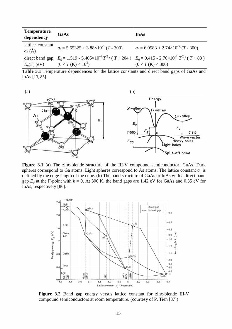
3.3.1 Solid source cells and shutters
The solid source MBE is equipped with Al, Ga and In cells of group III elements, C and Si
cells of group IV elements, and an As valved-cracker cell of group V elements. The cells are used
to produce directed atomic beams, or a molecular beam in the case of arsenic (which give rise to
the name “mo cu ar” am pitaxy). Th group IV m nts ar us for oping, i.e., the C cell
for p-type doping and the Si cell for n-type doping. The C cell is made of an electron beam
evaporator with a pyrolytic graphite bar heated directly from its side by an accelerated electron
beam [100]. All the other cells are Knudsen effusion cells (K-cells) made of pyrolytic boron
nitride (PBN) crucibles, filled with ultra-pure ingots or pellets of desired materials inside. Each
K-cells is heated by a meander shaped tungsten filament. The operation temperature for K-cells is
in the range of 200 °C to 1400 °C. The temperatures of the cells are measured by thermocouples,
and the heating power is regulated by a PID-feedback loop according to the readout data from the
thermocouples. Every solid source is independently heated until the desired beam flux is reached
for growth.
However, the evaporation of the materials should ideally take place when the condensed
phase and its vapor are in thermodynamic equilibrium. The flux is mainly regulated by the vapor
pressure which essentially increases exponentially with the temperature of the cell. Therefore, the
flux basically follows Arrhenius’ law in a thermodynamic process with an activation energy Ea:
⁄
where P is the vapor pressure of the source material, P0 is a constant of the vapor pressure, kB is
the Boltzmann constant and T is the temperature of the cell. Usually, the group III elements are
supplied as monomers, while the group V elements are generated as tetramers or dimers. The As
valved-cracker cell has a two-zones furnace called cracker zone to dissociate As4 into As2, and
also a valve to control the flux [80]. The flux is monitored by measuring the beam equivalent
pressures (BEP) of constituent elements by a moveable ionization gauge. A Bayard-Alpert
ionization gauge is used in this case with a measuring range down to 1 × 10-11
Torr. The ion
gauge can be moved mechanically either to the position close to the substrate for measuring the
BEP directly from the cell towards the substrate, or outside of the beam to determine the
background pressure.
Every cell is equipped with a computer controlled shutter positioned in front of it which
allows for switching the supply of the beam toward the substrate on and off within a fraction of
one second (about 300 ms). Thus, together with the beam impinging rate about 1 ML/s on the
substrate, the growth control with a monolayer precision is achieved. The temperature of the cells
and the switching of the shutters are both controlled by the Riber Crystal Eyes software which is
also capable of programming growth recipes.

23
3.3.2 Substrate heating and manipulation
Quartered GaAs (100) epi-ready wafers of 3 inches in diameter are used as substrates for
epitaxial growth in this work. Before loading to the growth chamber, a substrate is first degassed
at 150 °C for 45 minutes in the load-lock chamber under vacuum. After that, it is transferred into
the growth chamber via the transfer chamber using a magnetically coupled transfer rod as shown
in Figure 3.4. The substrate is placed onto a rotatable support in the close proximity (a few
millimeters) of a heater, facing the effusion cells. The substrate is heated during growth to
increase the mobility of adatoms or molecules on the surface and consequently reducing the
formation of lattice defects. The substrate is heated only by radiation. The heater is made of a
meandered tantalum filament with a PBN diffusor. The substrate support is made of refractory
materials, such as Mo and Ta, which do not decompose or give out gas impurities even when
heated up to 1,400 °C.
A thermocouple measures from the back side of the heater while the heating current is
regulated by a feedback loop. From the construction, the heater is not set in direct contact with
the substrate so there is a difference between the set temperature of the heater and the actual
substrate temperature. To be sure about the precise substrate temperature, an infrared pyrometer
is used to measure indirectly through a view port of a transparent window. A dual wavelength,
emissivity-independent pyrometer is the best option for this purpose [96]. In the following, the
thermocouple temperature and the pyrometer temperatures are registered as Tset and Tpyro,
respectively. For producing uniform and reproducible layers, it is very important to maintain
uniform temperature across the substrate with a maximum deviation of 5 °C. The substrate is thus
kept rotating by a rotation assembly during the growth process in order to have a high degree of
temperature uniformity on the substrate, which is also beneficial for the homogeneous growth of
the layer sequences as all the cells are tilted with respect to the substrate normal direction by the
same angle about 20°.
3.3.3 Growth parameters
During the epitaxial growth, there are numerous competing processes for the growth kinetics
of adatoms on a heated substrate as shown schematically in Figure 3.6. The adatoms or
molecules impinging on the substrate surface can be adsorbed on the surface. They can then
migrate on the surface until they incorporate into either the crystal surface lattice of the substrate
or the overgrown epitaxial layer. They can also aggregate with other adatoms to form nucleation
seeds which can grow further into islands or layers. Meanwhile, the interdiffusion or intermixing
can occur inside the crystal lattice. However, when the substrate temperature is sufficiently high,
the thermally desorbed atoms will not be incorporated into the crystal lattice. In the case of III-V
semiconductor compounds, group V elements are preferentially desorbed above the congruent
evaporation temperature Tc [96]. On the other hand, group III elements also tend to evaporate at
even higher temperatures. In order to avoid the re-evaporation, the substrate temperature should

24
not exceed a certain temperature. The congruent temperatures of different compounds are listed
below in Table 3.2.
With the temperature and surface conditions for MBE growth in this work, the sticking
coefficient of the group III elements, i.e., Al, Ga and In, on a GaAs substrate surface is unity,
which means that all the atoms stick onto the surface. In contrast, the sticking coefficient of the
group V elements, As4 and As2, all alone is zero. As4 or As2 can be incorporated on the surface
only if the adatoms of group III elements are present. This gives the advantage that the
stoichiometry is self-regulated as long as the system is under arsenic-rich conditions. For this
reason, the growth rate is then controlled by the flux of group III elements when an arsenic
overpressure is maintained during the growth. For GaAs growth, the ratio of III/V elements is
about 1/30, while for InAs growth, the ratio is about 1/190. These flux ratios are determined by
the BEPs measured from the ionization gauge multiplied with the gauge sensitivity factor for the
elements as listed in Table 3.3.
Figure 3.6 Schematic illustration
of the surface processes occurring
during the growth by MBE [97].
III-V Compound AlAs GaAs InAs AlP GaP InP
Tc (°C) 850 650 380 700 670 363
Table 3.2 List of approximate congruent sublimation temperature (Tc) for Langmuir
evaporation of III-V semiconductor compounds [96].
Element Al Ga In As
Sensitivity factor 0.92 1.68 2.44 1.76
Table 3.3 The ion gauge sensitivity factors for different elements [99]

25
3.3.4 Reflection high-energy electron diffraction
The surface crystallography and growth kinetics are monitored by reflection high-energy
electron diffraction (RHEED) [101]. In practical, it can be used to ensure the reproducibility of
growth, to calculate the growth rate, and also to determine the surface crystal structure,
cleanliness and smoothness. This technique employs a high-energy electron beam (up to 25 keV
with this system) emitted from an electron beam source directed onto the substrate surface at a
glancing angle of about 0.5° to 2°. The image of the diffraction pattern is shown on a fluorescent
screen symmetrically placed opposite the electron beam source. Due to the small glancing
incident angle, RHEED is very surface-sensitive as the electron beam is only scattered in the
first few atomic layers, not in the bulk crystal. The scattering results in diffraction patterns
which can be used to monitor the surface reconstruction. In the case of GaAs, numerous surface
reconstructions exist depending on the arsenic pressure and the substrate temperature [98]. The
appearance of the diffraction patterns can be used to provide qualitative feedback on the surface
morphology. If the sample surface is smooth, the diffraction pattern appears streaky, i.e.,
elongated spots. With increasing surface roughness, the diffraction pattern becomes more and
more hazy.
RHEED can provide an accurate, quick and direct method to determine the growth rate by
monitoring the intensity of the pattern by a camera from the screen. During layer by layer growth,
the intensity of the RHEED pattern, most prominently the specular spots, oscillates because the
roughness of the newly forming layers is larger than that of the closed ones. Each period of the
oscillations corresponds to the time needed for the growth of one monolayer. A scheme of the
relation between different monolayer growth stages and RHEED intensity oscillations is shown in
Figure 3.7. Furthermore, with RHEED patterns, it is also possible to identify the growth
transition from layer to island structures like quantum dots when the pattern changes from streaky
to spotty.
Figure 3.7 RHEED intensity
oscillations with the period of
the growth of one monolayer on
a GaAs (001) surface [102]. The
signal assumes a maximum for
the surface coverage = 0 and
= 1, e.g., a completed Ga plane
or a completed As plane for the
growth of GaAs layers.

26
3.4 Self-Assembled 3D Nanostructures
Self-assembled semiconductor nanostructures have been the focus for rigorous research
efforts in terms of basic physics and solid-state devices due to their unique optoelectronic- and
physical properties. As already discussed in the previous section, 3D islands can occur if the
growth system obeys the relation of
for either strained or unstrained systems by SK
or VW growth mode, respectively. In the following, two different self-assembly growth methods
to generate 3D nanostructures with lattice-mismatch and lattice-match will be discussed. The first
approach based on SK growth mode can result in strain-induced quantum dots. The second one
following VW growth is called droplet epitaxy (DE) which allows both strained and unstrained
systems to produce various nanostructures such as QDs, quantum rings (QR) and nanoholes (NH).
3.4.1 Strain-induced quantum dots (SK)
The SK growth mode used for producing quantum dots takes the advantage from the natural
tendency of strained systems, e.g., InAs/GaAs, InAs/InP, InAlAs/AlGaAs, InP/GaAs, Ge/Si,
GaN/AlGaN and GaAs/AlGaAs [1]. As illustrated in Figure 3.8, the basic mechanism is
presented for an InAs/GaAs system with a quite considerable lattice mismatch of 7 % which
leads to the formation of InAs QDs on a GaAs (100) substrate. (a) The GaAs substrate has a
lattice constant of aGaAs ~ 5.66 Å. (b) The initial InAs growth occurs layer by layer on the GaAs
substrate because of the small interface energy between the substrate and the grown material.
However, due to the lattice mismatch, the strain energy will increase with the InAs layer
thickness d. At a certain thickness, the strain energy is beyond the limit that the system can afford
to remain in the 2D growth mode. Thus, it will be energetically favorable to release the strain by
forming the subsequent InAs into 3D islands on the already-grown 2D layer. This process is also
known as lattice relaxation. The thickness at which this occurs is defined as the critical layer
thickness dc, and the underlying layer is called the wetting layer (WL) following the GaAs lattice
constants, i.e., epitaxially. The InAs islands form randomly in an attempt to recover the bulk InAs
lattice constants of aInAs ~ 6.06 Å. These self-assembled quantum dots grown by an SK approach
are therefore referred to as the strain-induced quantum dots.
During the SK growth, the strain relaxation is elastic and free of dislocations, leading to the
formation of an ensemble of coherent (defect-free) 3D islands. The growth mechanism
responsible for the coherent islands has been theoretically analyzed in the strained system [103].
A phase diagram corresponding to the analysis results is shown in Figure 3.9. Λ is the ratio of
the energy of the dislocated interface to the change of the surface energy. According to this phase
diagram, the formation of the coherent islands occurs with a sufficient amount of material while
the ratio Λ is larger than a critical value of Λ0, i.e., a small change of the surface energy or a large
energy of the dislocated interface. Meanwhile, such considerations indicate that a coherent 3D
island is in thermodynamic equilibrium when it is smaller than a certain size. Moreover, in such
semiconductor systems, one remarkable property is that these strained 3D islands do not undergo

27
Ostwald ripening (small islands rearranged into few large islands) after being formed, and display
a narrow size distribution. Thus, in principle, an ensemble of coherent islands is energetically
more favorable than a single large island in the system.
Figure 3.8 Schematic drawing showing the growth of the InAs quantum dots by the
SK growth method. (a) GaAs substrate (orange color); (b) growth of the strained InAs
(blue color) wetting layer on GaAs (100); (c) with increasing InAs coverage above a
critical thickness, the strained layer relaxes to minimize the surface energy by the
spontaneous formation of randomly distributed islands. (courtesy of R. Roescu [104])
Figure 3.9 A phase diagram for three
different morphologies. UF: Uniform Film,
CI: Coherent Island, DI: Dislocated Island,
Q: the amount of the deposited material, Λ:
the ratio between the energy of dislocated
interfaces and the change of the surface
energy. (adapted from [8, 103])

28
The phenomena of the island density, size distribution and the absence of ripening have been
explained by theoretical kinetic and thermodynamic models. In the kinetic models, the evolution
of island growth is predicted by various processes such as diffusion, deposition, attachment and
detachment under strong non-equilibrium conditions, which result in self-limiting growth to the
size and density of the coherent islands with respect to the growth rate and coverage [22]. For
example, a preferential migration of adatoms towards smaller islands due to kinetic barriers limits
the attachment to the strained islands [105], while the competition between the bonding energy
and the strain energy leads to the enhancement of adatom detachment from large islands [106]. In
the thermodynamic models, an ensemble of 3D islands with ordered size, shape and relative
arrangement is described as a new class of equilibrium surface structures [107]. When the
formation of a single 3D island is introduced on such surface structures, the total energy of the
system will be changed. According to this change, there exists an optimum island size
corresponding to the absolute minimum of the energy for the mismatched systems. In this model,
the change of the surface energy is mainly due to the appearance of side facets and the
disappearance of certain areas of the wetting layer. The shape and size of the islands then appear
to be strongly interdependent. However, there is no driving force for ripening in this case.
According to the thermodynamic and kinetic mechanisms, the growth parameters appear
crucial in the final surface morphology of the 3D islands. Experimentally, the dependence of the
density ρ
of islands has been described as a function of the deposited amount by the relation
similar to a first order phase transition as ρ ρ
( )
, where d > dc. dc is the critical
thickness. is the exponent. ρ
is the normalization density of islands. Processing the
experimental data, the fitting parameters = 1.76, ρ = 2 × 10
11 cm
-2, and dc = 1.5 ML has been
found for the InAs islands deposited on GaAs (100) at a substrate temperature of 530 °C [70].
However, the value of the critical thickness strongly depends on the growth conditions.
From previous works, the value of dc for InAs/GaAs system is found to be 1.5 ML to 1.8 ML
[68, 108–110]. Moreover, when the thickness exceeds another feature thickness dd, dislocations
start to emerge in the structure, i.e., dislocated islands, while the quality of the QDs reduces. In
order to obtain high quality QDs, it is therefore important to keep the layer thickness d within a
range dc < d < dd, which has been suggested to be in the interval of 1.7 ML < d < 3.0 ML [111]. If
further materials are deposited, the system can have a tendency to ripening which would induce
certain disadvantages for the quantum dot fabrication such as reducing the density, broadening
the size distribution and resulting in defects in the large islands [112].

29
3.4.2 Nanostructures by droplet epitaxy (VW)
Contrary to the SK growth mode, another self-assembly method for 3D nanostructures called
droplet epitaxy (DE) has emerged recently. This method was first proposed by N. Koguchi and
K. Ishige used for the growth of GaAs microcrystals on an S/GaAs substrate [23]. Subsequently,
self-assembled GaAs quantum dots were successfully fabricated on an AlGaAs surface using
droplet epitaxy [7]. In MBE growth, droplet epitaxy is an alternative method which can make up
the deficiency of the SK approach to fabricate various self-assembled nanostructures. For
example, the SK growth method is limited by the presence of lattice mismatch, which is not
essential in droplet epitaxy. Therefore, DE allows the growth of lattice-matched systems, e.g.,
GaAs/GaAs, inefficient lattice-mismatched systems, e.g., GaAs/AlxGa1-xAs, as well as lattice-
mismatched systems. Furthermore, droplet epitaxy can offer a higher degree of freedom in
controlling the size and density of nanostructures because the transition process of liquid phase
metal droplets into solid semiconductors is not limited to the native strain or the material system.
Additionally, for the study of single nanostructures, either a super-low density or a subsequent
process to focus on only one singular nanostructure is required. A DE approach can provide a low
density of the order of 105 to 10
7 cm
-2 which is several orders of magnitude lower compared to
that of the SK method [27].
Droplet epitaxy is based on the incorporation of group V elements into the group III element
droplets formed on the substrate to obtain the growth of III-V nanocrystals [23]. In practical, the
growth of droplet epitaxy contains two processes which are the metal droplet formation and the
crystallization. For example, in the case of a GaAs/AlGaAs heterostructure, Ga is supplied on an
AlGaAs substrate with the absence or the presence of only small quantities of arsenic flux. After
the deposition of Ga atoms on the AlGaAs surface, a part of the deposited Ga atoms will combine
with the remaining arsenic atoms on the AlGaAs surface and the rest will form Ga droplets by
atomic migration. The formation of droplets is based on the VW growth mode because the
binding energy of Ga adatoms is larger than that between Ga adatoms and the AlGaAs surface
atoms. This process is subject to the phenomenon of Ostwald ripening (the small droplets
incorporate into the large ones) when the amount of the deposition material is sufficiently high
[112]. The size and density of droplets depend on the substrate temperature applied in this
process, e.g., smaller droplets with a high density are obtained at a lower temperature. On the
other hand, the size of the droplets can simply be changed by the coverage of the deposited metal
material, i.e., a higher monolayer coverage leads to larger droplets [113].
After forming Ga metal droplets, an As flux is applied to crystallize the droplets into
semiconductor nanostructures, i.e., GaAs. In general, crystallization is immediately executed after
the formation of droplets in order to prevent further Ostwald ripening. Because of the high
surface energy density of the metal droplets, the crystallization starts at the interface of three
phases, i.e., the skirt of the droplet (the circular line of the interface between Ga droplets and the
AlGaAs substrate), as shown in Figure 3.10 (a) [114–116]. Therefore, the crystalline

30
nanostructures are pinned on the substrate surface with their density basically consistent with that
of the droplets. Meanwhile, the growth process of the crystalline nanostructures is determined by
the atomic diffusion of Ga atoms and the incorporation of As atoms which can be changed under
different growth conditions. In other words, higher temperature leads to higher Ga atomic
mobility on the substrate surface, while higher arsenic flux enhances the crystallization resulting
in a reduction of the diffusion regions of the Ga atoms (Ga atoms are captured by arsenic atoms).
Therefore, the final morphology of the crystalline nanostructures can be controlled by the
substrate temperature and the arsenic flux applied in the process of crystallization. For example,
at a low temperature (200 °C ~ 300 °C), the metal droplets will be crystallized into
semiconductor quantum dots under a high arsenic pressure (~10-4
Torr) [30] when the region of
the Ga atomic migration is smaller than the dimension of the droplets as shown in Figure 3.10 (b).
Alternatively, single QRs or double QRs will be obtained under a medium arsenic pressure
(~8×10⁻⁶
Torr) [29] or a low arsenic pressure (~2×10⁻⁶
Torr) [37], when the Ga atomic diffusion
region is comparable with or larger than the droplet dimensions as shown in Figure 3.10 (c) and
(d), respectively. Furthermore, at a high temperature (~ 500 °C), the droplets can generate deep
nanoholes by the thermal solution of the crystalline substrate underneath the liquid droplets. This
process is also called local droplet etching or nanodrilling [34, 36]. More unique nanostructures
have been created in different conditions, such as quantum dot molecules and ensembles,
transition structures between single and double quantum rings, and QDs with ultra-low density
[24–27, 44–46]. All in all, owed to the flexibility of liquid phase metal droplets in droplet epitaxy,
the realization of these various self-assembled nanostructures becomes possible.
Two kinds of productions, shallow and deep nanoholes, are fabricated with low As pressure
and high substrate temperature in this work. Figure 3.11 illustrates the mechanisms regarding the
crystallization processes for nanohole structures with a GaAs/GaAs system under these growth
conditions. After a Ga droplet is formed on a GaAs surface by VW growth, a low As flux is
supplied on the Ga droplet. Ga atoms of the droplet react with arsenic atoms into GaAs molecules.
Meanwhile, thermal etching takes place at the GaAs surface in a contact with the Ga liquid where
there is a Ga-rich condition at high temperature [34]. The Ga liquid droplet solves the GaAs
crystalline substrate into GaAs molecules. Due to the driving force induced by the surface energy
differences at the interfaces of three phases, the nucleation of GaAs crystals first starts at the skirt
of the droplet and then along the edge of the droplet. The crystal growth is carried out by the
thermal diffusion of the GaAs molecules from the internal thermal solution and from the
external arsenic-flux reaction toward the edges of the droplet resulting in a downhill material
transportation [33]. After all, the crystallization is effective at the droplet edge leading to the
formation of a circular nanostructure, i.e., a ring-like structure [42]. During the crystallization, the
amount of Ga atoms in the droplet decreases as does the droplet size. Finally, all the Ga atoms are
solidified, i.e., fixed in the crystal. A nanohole is then left on the surface. The shallow nanohole is
constructed by the ring-like crystalline structure. On the other hand, the deep nanohole is formed
with a significant thermal etching. In general, a larger and deeper nanohole can be developed
with a larger droplet due to sufficient materials for growing and etching [34, 39].
31
Figure 3.10 Schematic illustration of the morphology evolution during the crystallization of the
Ga droplets under different sizes of the Ga diffusion region [115]. (a) The preferential
crystallization occurs at the skirt of the droplet. The formation process for (b) QD, (c) QR and
(d) double QR. The red and green hemispheres represent the Ga droplet and the GaAs
nanostructure. The red and blue spheres represent the Ga atoms and the As atoms. The orange
arrows point to the Ga diffusion region boundary.
Figure 3.11 The crystallization process for a nanohole structure by droplet epitaxy
(adapted from [39]). (a) the formation of a Ga droplet (b) the material transportation
of the GaAs molecules originated partly from the reaction between Ga droplet and As
flux, and partly from the solution of the GaAs substrate towards the edge of the
droplet (c) the growth of the ring-like structure at the edge of the droplet with the
reduction of the droplet volume (d) a nanohole structure formed after the
solidification


33
Chapter 4 Surface Patterning Techniques for Site-
Selective Growth
This chapter begins with an introduction which includes the concept related to the site-selective
growth of strain-induced QDs and a review of previous works with various patterning approaches.
The site-selective growth is mostly obtained with the help of templates which can provide
preferential nucleation sites. In this work, the templates were made of self-patterned GaAs
nanoholes generated by droplet epitaxy for the site-control of QDs. The GaAs nanohole templates
can be realized with either a random distribution or an organized arrangement. The randomly-
distributed GaAs nanoholes on a GaAs surface are formed due to the nature of droplet epitaxy.
On the other hand, the achievement of arranged GaAs nanoholes relies on the pre-patterning of a
GaAs surface with an in-situ focused ion beam (FIB) in the way that Ga droplets can nucleate
preferentially depending on the patterns and then be transformed into GaAs nanoholes through
crystallization. The ideas of using self-patterned nanohole templates for the site-selective growth
of QDs, and combining a FIB pre-patterning technique to control the sites of self-patterned
nanoholes, are explained and demonstrated in the second section. A detailed description of the
focused ion beam system used in this work is shown in the last section, including the features,
working principle and the equipment. The essential FIB parameters and the pattern design applied
for pre-patterning in this work are given in this part as well.
4.1 Introduction to Site-Selective Growth
0D semiconductor quantum dots with a sharper density of states have superior transport and
optical properties with respect to higher dimensional structures. Therefore, intense research with
the subject of semiconductor quantum dots has been done for their possible use. The ensembles
of self-assembled quantum dots have been used in optoelectronic devices such as quantum dot
lasers [11, 14]. On the other hand, single semiconductor quantum dots have attracted a lot of
interests for their applications in future novel nanoelectronic devices used for solid-state quantum
information processing, e.g., single photon sources for quantum cryptography [17, 18, 117] and
the building blocks for quantum computing [19, 20, 118]. In particular, the success of all these
new quantum devices based on single QDs or QDMs requires the ability to fabricate
nanostructures with control of size and spatial location. However, the growth of self-assembled
QDs, by either Stranski-Krastanov growth mode or droplet epitaxy, tends to cover the surface in a

34
near-random fashion with some preferences for nucleation at underlying step edges [9]. This
random nucleation makes it difficult to address each individual self-assembled QD separately.
Therefore, it is necessary to combine strategies that would permit the precise location of
nanostructures carrying high optical quality, i.e., the site-control and the site-selective growth of
QDs.
For the purpose of a site-selective growth, a commonly utilized strategy to overcome the
random positioning of self-assembled nanostructures is based on the pre-patterning of substrates.
The aim of pre-patterning is to create templates with well-ordered arrays of preferential
nucleation sites for island overgrowth. Through a re-growth on such templates, the site-selective
growth of self-assembled quantum dots can then be achieved. The preferential nucleation sites are
derived from the atomic diffusion differences between different faceted surfaces on the template.
For example, the selective nucleation of InGaAs QDs was found at or near the multistep edge of
the GaAs epilayer grown on GaAs (001) substrates with a misorientation of 2° along the [010],
[110] and [1 0] directions, resulting in the self-alignment of quantum dots along the step edges
by MOCVD [119]. Another example of the self-alignment of self-assembled InAs islands was
achieved by using wet chemical etching with grating pitches from 0.28 µm to 5 µm on GaAs
surface with MBE [120]. It was observed on the samples with the smallest pitch of 0.28 µm that
the islands are located at the sidewalls or at the bottom of the valleys. However, with larger
spacings, island nucleation occurred at the sidewalls of the ridges along the [ ] direction, while
the islands were found on the (100) planes and at the foot of the mesa-structure with the ridges
along the [ ] direction. The preferential nucleation of self-assembled QDs has been found at
multistep edges, on top of ridges, in the bottom of valleys and at the sidewall of mesa-structures
where there are different faceted surfaces. It is suggested that the surface with appropriate
modification can provide an influence to QD positioning [120].
In terms of surface pre-patterning, except creating preferential nucleation sites, it also
ensures the reproducibility of those nucleation sites with an exact position control. For instance, a
lateral site-control of strain-induced InAs QDs in arrays has been established using lithography
combined with etching. Trenches patterned on the GaAs (100) surface were employed as
preferential nucleation sites for the InAs QDs to grow in chains by chemical beam epitaxy [121].
Later, the selectively grown InAs QDs on the top of the (100) faceted mesa stripes of the GaAs
substrate have also been demonstrated [122, 123]. Extended from the pre-patterning method, an
idea of surface strain engineering was obtained through the combination of stressors with
patterning, which created a lattice of nucleation sites for QDs [124, 125]. During an MBE
re-growth of InAs, the thermodynamic and diffusion kinetics of the In atoms were modified by
the sub-surface strain fields introduced by growing a strained In(Ga)As film below the surface.
As a result, the InAs layers grow more rapidly on the top of the mesas, forming a preferential
growth of InAs islands on the top of sub-surface stressors.
In order to address single dots individually, it is important to reduce the field of preferential
nucleation sites allowing limited number of QDs grown within demanded dimension. For
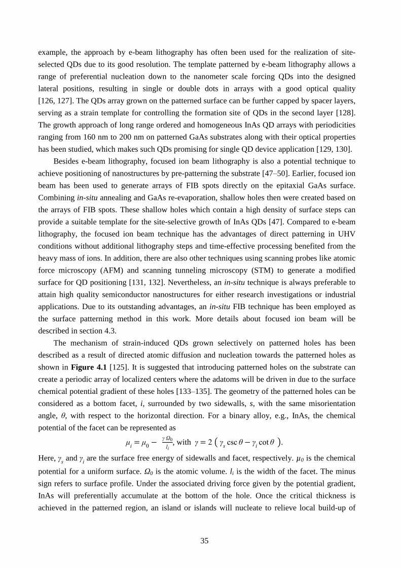
35
example, the approach by e-beam lithography has often been used for the realization of site-
selected QDs due to its good resolution. The template patterned by e-beam lithography allows a
range of preferential nucleation down to the nanometer scale forcing QDs into the designed
lateral positions, resulting in single or double dots in arrays with a good optical quality
[126, 127]. The QDs array grown on the patterned surface can be further capped by spacer layers,
serving as a strain template for controlling the formation site of QDs in the second layer [128].
The growth approach of long range ordered and homogeneous InAs QD arrays with periodicities
ranging from 160 nm to 200 nm on patterned GaAs substrates along with their optical properties
has been studied, which makes such QDs promising for single QD device application [129, 130].
Besides e-beam lithography, focused ion beam lithography is also a potential technique to
achieve positioning of nanostructures by pre-patterning the substrate [47–50]. Earlier, focused ion
beam has been used to generate arrays of FIB spots directly on the epitaxial GaAs surface.
Combining in-situ annealing and GaAs re-evaporation, shallow holes then were created based on
the arrays of FIB spots. These shallow holes which contain a high density of surface steps can
provide a suitable template for the site-selective growth of InAs QDs [47]. Compared to e-beam
lithography, the focused ion beam technique has the advantages of direct patterning in UHV
conditions without additional lithography steps and time-effective processing benefited from the
heavy mass of ions. In addition, there are also other techniques using scanning probes like atomic
force microscopy (AFM) and scanning tunneling microscopy (STM) to generate a modified
surface for QD positioning [131, 132]. Nevertheless, an in-situ technique is always preferable to
attain high quality semiconductor nanostructures for either research investigations or industrial
applications. Due to its outstanding advantages, an in-situ FIB technique has been employed as
the surface patterning method in this work. More details about focused ion beam will be
described in section 4.3.
The mechanism of strain-induced QDs grown selectively on patterned holes has been
described as a result of directed atomic diffusion and nucleation towards the patterned holes as
shown in Figure 4.1 [125]. It is suggested that introducing patterned holes on the substrate can
create a periodic array of localized centers where the adatoms will be driven in due to the surface
chemical potential gradient of these holes [133–135]. The geometry of the patterned holes can be
considered as a bottom facet, i, surrounded by two sidewalls, s, with the same misorientation
angle, θ, with respect to the horizontal direction. For a binary alloy, e.g., InAs, the chemical
potential of the facet can be represented as
μ μ
, with (
csc θ
cot θ ).
Here, and
are the surface free energy of sidewalls and facet, respectively. µ0 is the chemical
potential for a uniform surface. 0 is the atomic volume. li is the width of the facet. The minus
sign refers to surface profile. Under the associated driving force given by the potential gradient,
InAs will preferentially accumulate at the bottom of the hole. Once the critical thickness is
achieved in the patterned region, an island or islands will nucleate to relieve local build-up of

36
strain according to the SK growth mode. As a result, the site-control of self-assembled QDs is
obtained.
Figure 4.1 Schematic of the periodic surface patterning process using electron beam
lithography for producing site-selected strain-induced QDs [125]. (A) Developing
patterns by electron-beam lithography on a GaAs substrate (B) Transferring patterns
using wet chemical etching. (C) Introducing the patterned GaAs substrate into the
MBE chamber for re-growth of a GaAs epitaxial buffer layer followed by InAs
deposition. (D) InAs QDs are formed in the hole after the critical thickness for 3D
islands growth is reached in the depression following the SK growth mode.
4.2 Self-Assembled Nanohole Patterning
Alternative to artificial pre-patterning, self-assembly patterning (self-patterning) by droplet
epitaxy has been revealed as a potential technique to produce nanoholes as templates for the site-
selective growth of QDs without the need of any lithographic steps [40–46]. In this work, the
self-patterned nanohole templates were developed in GaAs/GaAs systems by droplet epitaxy. The
description about droplet epitaxy can be found in subsection 3.4.2. These nanoholes fabricated by
droplet epitaxy having high densities of monolayer steps (high-index surface) can provide
preferential nucleation sites for the further nucleation of deposited InAs, resulting in the
formation of strain-induced InAs QDs following the SK growth within the same series of MBE
growth, i.e., an in-situ process. The density of these strain-induced QDs is therefore
corresponding to that of the GaAs nanoholes formed by droplet epitaxy so that the value possible
to be obtained is as low as 107
cm−2
[38]. The size of the QDs is related to the amount of InAs
deposited in the GaAs nanoholes with the independence of their density, which is opposed to the
QD formation by the SK growth method [43]. This fact is especially interesting for the
applications based on single QDs. Particularly, a different number of QDs per nanohole can also
be obtained resulting in QD pairs or QDMs, which is coincidentally the same with other
37
lithographic techniques [41, 136]. Moreover, in the self-assembly growth, the strain-induced
approach can provide defect-free QDs whose crystal qualities are generally better than that of the
QDs carried out by the crystallization in droplet epitaxy. Combining the advantages from droplet
epitaxy and the strain-induced approach in the MBE growth, this technique is therefore becoming
a promising method to achieve site-selected QDs or QDMs with low densities and high optical
qualities for their potential applications e.g., single QD devices. In this work, this combination
was used for realizing the site-selective growth with InAs QDs in GaAs nanoholes.
Nevertheless, the nanoholes formed by droplet epitaxy are randomly distributed, which in
turn leads to randomly-distributed QDs on the sample. In order to further control the location as
well as to design the arrangement of the quantum dots arbitrarily, an in-situ focused ion beam
pre-patterning was applied before the fabrication of self-assembled/self-patterned nanoholes in
this work. It has been found that using the FIB technique can locally modify the surface in a way
that the site-selective growth of crystals can be achieved based on the FIB patterns with various
FIB parameters [137]. In addition, due to the difference of surface energies on the FIB modified
surface, the preferential nucleation of metal droplets is expected via a site-selective growth by the
VW growth mode [138]. With crystallization under certain growth conditions by droplet epitaxy,
these site-selected metal droplets can be transformed into crystalline nanoholes resulting in well-
organized self-assembled nanoholes on the surface depending on the FIB patterning parameters.
By using these FIB-arranged nanoholes as templates, the arrayed QDs with an arbitrarily defined
distribution can then be realized via a site-selective growth by MBE. This serial approach,
involving two subsequent site-selective growths with two different surface patterning techniques,
can be developed by the MBE-FIB system at AFP via an in-situ process. For the two subsequent
site-selective growths, first, the Ga droplets are preferentially nucleated on the FIB-patterned
surface, which can be crystallized into GaAs nanoholes through droplet epitaxy. Secondly, the
strain-induced InAs QDs are preferentially formed in these GaAs nanoholes which are self-
patterned on the FIB-patterned surface. In other words, the droplet epitaxy method plays a role in
the site-selective growth as well as in the surface patterning, in a self-assembly way. The
schematic illustration shown in Figure 4.2 serves to explain the development processes used in
this work.
At beginning, the growth of the GaAs epitaxial layer was carried out by MBE with a GaAs
substrate. Then, the sample is transferred into the FIB system under the vacuum conditions. An
in-situ focused ion beam is employed to generate several FIB-patterned areas on the GaAs
surface. The applied patterns in this work are designed with square arrays of spots within an area
of 60 × 60 μm2. According to this pattern design, several small locally modified spots of the order
of nanometers are therefore generated on the surface by a focused beam, which are called the
“FIB spots”. Each FIB-patterned area, consisting of the square arrays of FIB spots, can be created
with different FIB parameters which will be given in subsection 4.3.3. After FIB patterning, the
surface modified sample is transferred back into MBE for the fabrications of self-patterned
nanoholes and strain-induced QDs in sequence.

38
Figure 4.2 Schematic illustration of the site-selective growth processes for QDs grown in GaAs
nanoholes with or without FIB pre-patterning by a MBE-FIB system (not in scale). (a) Using
MBE, a GaAs layer is grown on a GaAs (100) substrate. Then, the sample is transferred to the
FIB system under vacuum conditions. (b) in-situ FIB patterning is carried out by a Ga+ or an In
+
ion beam to create FIB spots on the surface. The sample containing the FIB-patterned area and
the bare GaAs surface (without FIB-patterning) is then transferred back to the MBE system under
vacuum conditions. (c) MBE re-growth is executed for the formation of GaAs nanoholes by
droplet epitaxy and InAs QDs by SK growth in sequence. GaAs nanoholes are formed on the
FIB-patterned area and also on the bare GaAs surface, resulting in arrayed or randomly-
distributed nanoholes. Then, the deposited InAs is preferentially nucleated inside both types of
GaAs nanoholes resulting in site-selected QDs with an arrayed arrangement or a random
distribution embedded in the sample.
GaAs nanoholes self-assembly by droplet epitaxy via homoepitaxy are generated with the
conditions of a low As pressure and a high substrate temperature for this work. The mechanism
of the nanoholes generated by droplet epitaxy can be found in subsection 3.4.2. Due to the nature
of self-assembly, GaAs nanoholes are spread all over the sample, i.e., on the FIB-patterned areas
and also on the bare GaAs surface outside the FIB-patterned areas at the same time. However, on
the FIB-patterned areas, the GaAs nanoholes are formed site-selectively due to the surface energy
difference induced by FIB pre-patterning represented as well-arranged “arrayed nanoholes”
depending on the arrays of FIB spots. On the other hand, the formation of the GaAs nanoholes on
the bare GaAs surface without FIB pre-patterning does not occur site-selectively but in a
randomly-distributed manner resulting in “randomly-distributed nanoholes”. The deposition of
InAs is then executed in the MBE system directly after the formation of the nanoholes. Due to the
chemical potential gradients as a result of the high-index surfaces of the nanoholes, the nucleation
of the InAs deposition will occur preferentially in these nanoholes (both arrayed and randomly-
distributed ones). When the critical thickness of the deposited InAs inside the GaAs nanoholes is
reached for the 2D-3D transition, the strain-induced InAs QDs are then formed by SK growth
with site-selection. These site-selected QDs follow the distribution of GaAs nanoholes resulting
in arrayed or randomly-distributed QDs generated on the FIB-patterned area or the bare GaAs
surface, respectively. The growth mechanism of strain-induced QDs by SK growth is addressed

39
in subsection 3.4.1. Finally, the in-situ site-selective growth of QDs with a controllable
distribution is therefore demonstrated owed to the combination of two compatible MBE growths,
FIB direct writing techniques, as well as the facility of the MBE-FIB system. More details about
the parameters and process of FIB patterning will be given in subsection 4.3.3. The sample
fabrication concerning the details of MBE growth will be given in section 5.1.
4.3 Focused Ion Beam Patterning
The technique of focused ion beam (FIB) is particularly used for the fabrication of
nanostructures in semiconductor industries and material science researches, which was mainly
developed during the late 1970s and the early 1980s. With the increasing circuit density and
decreasing feature dimensions in the semiconductor industry during that time, this technology has
been used as offline equipment for repairing masks, modifying and analyzing electronic devices,
debugging integrated circuits (IC) and preparing the transmission electron microscope (TEM)
specimens [139, 140]. Since the increasing demand for micro- and nano-structures in the 1990s,
FIB has been used in research as a powerful tool allowing the fabrication of high quality and high
precision nanostructures which can be applied for micro-electro-mechanical systems (MEMS),
photonic devices and sensors, scanning probe microscope (SPM) tips, magneto resistive head
trimming and micro-tools [141–144].
The art of using FI for nanofa rication is a so ca “ ir ct writing”, which transfers
patterns by removing or adding materials using a small FIB spot directly impinging on the
substrate, offering a maskless process [48]. The approaches to remove and add materials include
milling, ion-assisted etching, implantation, and ion-induced deposition, based on the phenomena
resulting from the ion-solid interactions. The key to the direct-writing technology is the ability of
FIB to operate a fine beam size with proper current and energy which is used to remove or add a
required amount of material with high precision in two dimensions. These FIB features are
enabled due to the invention of the liquid metal ion source (LMIS) which provides high current
density and a variety of ion species [145]. Due to the heavier masses of ions compared to those of
electrons or photons, larger energies and shorter wavelengths allow direct writing on hard
materials (such as semiconductors, metals or ceramics) without major forward and backward
scattering resulting in shorter penetration length in solid [146]. Thus, the feature size of the
pattern is only dictated largely by the beam size and the interaction of the beam with the target
material. In contrast, electrons or photons can mainly be applied for writing on soft materials
(such as polymers or resists) and the corresponding feature sizes are determined by the proximity
of backscattered electrons (BSE) or the wave diffraction limit [147]. Moreover, the lateral
straggling of the implanted ions in FIB technology is very low. Therefore, the proximity effect

40
can be reduced [148]. By controlling these well-focused ion beams, nanoscale patterning on
target materials with a high accuracy and complicated 3D structures can be achieved.
4.3.1 Equipment
The basic components of a FIB system consist of an ion source, an ion optics column, a
substrate stage, and a vacuum chamber in the range of UHV. An Orsay Canion 31 Plus FIB
column is used to define the pattern for site-selected QDs in this work. The FIB column is
interconnected to an MBE system as shown in Figure 3.4. A schematic diagram of the FIB ion
column is shown in Figure 4.3 which serves to introduce the basics of the FIB system.
Figure 4.3 The schematic diagram of a focused ion beam column.
(courtesy of S. Shvarkov)
The basic components of the ion optics column consist of an extraction electrode, condenser
lenses, an E × B filter, a beam blanker, a Faraday cup, a scanning and stigmation octupole,
objective lenses, two sets of selection apertures and a mechanical vacuum separation valve to
isolate the source chamber from the column (for changing LMIS). The lenses are made of biased
ring or cylinder shaped metal plates. Their focal length can be adjusted by varying the
electrostatic potentials. After extracted from a LMIS, ions are accelerated through the column by
the acceleration voltage, Uacc, which is adjustable between 5 kV and 30 kV with intervals of 5 kV.
These ions are focused and collimated into a parallel or crossover beam by the condenser lens.
Then, the ion beam is passed through a mass separator called an E × B filter or a Wien-filter. A
Wien filter is only used when the system is equipped with an alloy source. It is used to separate

41
the ion species emitted from the alloy source by applying an electrical field (E) and a magnetic
field (B). Both fields are orthogonal to the ion beam and to each other, so that the Coulomb and
Lorentz forces are anti-parallel. These two opposite forces acting on the accelerated ions
compensate each other only if the velocity of the ions is equivalent to the ratio of E/B. Because of
different mass to charge ratios, only the selected ions can pass through the mass selection
apertures toward the target while the other unwanted species are filtered out. Below the E × B
filter, there is the deflection and stigmator octupole. The deflector is capable of controlling the
final trajectory of the ions as well as performing the scanning of the beam over the sample. The
stigmator is used for correcting astigmatism and collimation to eliminate the ions that are not
directed vertically. The objective lens located below the stigmator helps to reduce the beam size
and also to improve the focusing of the beam. With a two-lens optical system, the diverging mode
has an advantage to form a small beam size at any beam currents among the four typical beam
operation modes, i.e., the crossover mode, the diverging mode, the parallel mode and the
converging mode [149]. The current selection apertures are applied to regulate the beam current
in a range from few nA to the order of pA. The beam blanker permits quickly switching off the
beam or deflecting the beam into an internal Faraday cup by which the beam current can be
measured. With this system, the ion beam can scan within a working area of 505 by 505 μm2, and
thereby write patterns via the lithography system called “Elitha”. These patterns are designed and
generated by a computer aided design program, e.g., AutoCad. A sample is placed on a computer
controlled x-y table which allows the displacement up to 50 mm in both directions perpendicular
to the FIB column. In this way, more than one area can be operated by step-and-repeat within the
quarter of a 3-inches wafer used in this work.
Liquid metal ion sources (LMIS) are the most common source for FIB techniques. They are
high brightness ion sources, which generate a beam of ions by the use of field emission. The ion
beam can then be focused to a nano-spot with an adequate current density for FIB direct writing
or imaging. These sources are made of metals which have relatively low melting temperatures
and low reactivity [150]. Currently, the available elements of LMIS made by the AFP group
include As, Au, B, Be, Bi, C, Co, Cr, Cu, Dy, Er, Fe, Ga, Ge, Gd, Ho, In, Mn, Ni, P, Pd, Pt, Si,
Sn and Tb [151]. In order to lower the melting point and to control the reactivity or to have
alternative elements from one LMIS, the elements are often prepared in a eutectic alloy, e.g.,
AuSiBe, AuErSi or GaIn. However, Bi, Ga, In and Sn can be prepared either in alloys or in
elemental LMIS. Among these elements, As, B, Be, P and Si are important for III-V
semiconductor technology because they are potential dopant elements. Ga- and In-LMIS are easy
in handling because of the low melting temperatures (29.8 °C for Ga and 156.6 °C for In), low
volatility and their long lifetime. Due to their high beam stability, good focusing properties
together with small energy spread and enough mass for high milling rates, Ga- and In-LMIS have
been used in FIB very frequently. For this work, Ga- and In-LMIS are employed for direct
writing in the nanoscale regime on the GaAs surfaces in order to locally modify the surface such
that the GaAs nanoholes can preferentially be formed along the FIB patterns by droplet epitaxy.
These FIB-arranged nanoholes can then serve as templates to establish site-selected InAs QDs

42
spatially following the pattern design. Moreover, Ga and In ions have the properties of high
sputter yield, small longitudinal ion range and that they are electrically almost neutral in GaAs,
which makes them suitable for patterning on GaAs surfaces [137].
A typical LMIS consists of a cylindrical spiral with a tungsten needle through it and a
tungsten filament, as shown in Figure 4.4. The spiral tube acts as a reservoir for the metal or
eutectic alloy. The spiral reservoir can be heated up through the filament to melt the metal or
alloy, and then feed the liquid metal to the tip of the needle. To extract the ions from the LMIS, a
high positive voltage of a few kV is applied to the needle relative to the extraction electrode,
which causes an electrostatic force at the tip. Depending on the balance between the electrostatic
force and the surface tension of the liquid metal at the tip, a sharp peaked cone called the Taylor
cone is formed [152]. Due to the extremely small radius at the apex of the Taylor cone (about
2 nm), a huge electric field (above 1 × 10⁸ V/cm) is formed by the extraction voltage resulting in
ionization and thermally assisted field emission of metal atoms in the vapor phase. Finally, the
positively charged ions are accelerated towards the extraction electrode with typical operation ion
currents about 2 µA to 10 µA. Most of the ions that run into the electrode are lost. Only a small
fraction transverses the central electrode aperture hole along or close to the optical axis of the ion
column. These extracted ions can then be condensed into a focused beam by the lens and ground
electrodes in the ion optics column.
(a) (b)
Figure 4.4 (a) An emitting HoNi alloyed
LMIS. (photo by A. Melnikov) (b) A Ga
LMIS consists of a spiral tube, a tungsten
needle and a tungsten filament.
4.3.2 Process
When ions hit a target material, they will collide with both the nuclei and electrons of the
target. The ion-solid interactions can be classified in two main distinct processes. One is the
elastic interactions with nuclei, which cause the displacement of lattice atoms, surface sputtering
and the generation of defects. Another one is the inelastic interactions with electrons, which
produce secondary electrons, X-rays and optical photon emission. Therefore, when ions strike on
a solid material, the events of sputtering, implantation, surface amorphization, swelling,
deposition, backscattering and nuclear reactions can take place [150, 153]. The trajectory of ions
is only changed as the result of a collision with an atom. Although between successive

43
interactions with nuclei, ions interact with the electrons as well, the ions will nearly not change
their trajectory which can be considered linear due to the big discrepancy between ion and
electron masses. The distance from the position where the ion enters the target to the position
where it stops is called “range”. The projection of the range along the incident direction of the
ions is called the projected range, Rp, while the distance traveled along a perpendicular axis is the
perpendicular range R⊥. The standard deviation in a projected range is called projected straggle,
ΔRp, while the statistical fluctuation of a perpendicular range is called lateral straggle, ΔR⊥. The
spatial distribution of the implanted ion is known as an implantation profile. The range and the
spatial distribution of an ion in an amorphous solid were studied theoretically by J. Lindhard et al.
[154]. According to their theory, the projected range of implanted ions can be described in first
approximation by a Gaussian function:
( )
√
[ ( )
( )
]
where D is the ion dose defined by the impinging ion charges per unit area. The maximum ion
concentration is at Rp. A software package called SRIM (Stopping and Range of Ions in Matter)
has been widely used for predicting the projected range and the sputter yield of many different
ions at a wide energy range hitting on the matters which in general could be gases, liquids or
solids with only their mass density being the distinguishing parameter. SRIM uses three
dimensional Monte-Carlo simulation of the ion-atom collision to calculate the stopping range of
ions in matter [155]. Despite of the distribution, it can also predict the kinetic phenomena
attributed from the energy loss of the ions, not only sputtering and implantation but also the target
damage, phonon production, ionization and ion reflection. The implantation profiles for Ga+ and
In+ ions incident perpendicularly into a GaAs substrate with an ion energy of 30 keV are shown
in Figure 4.5 using SRIM simulations. The calculated parameters for these cases of Ga+ and In
+
ions are listed in Table 4.1.
Applied for the sample processing in this work, the FIB writing is associated with sputtering,
redeposition, amorphization (swelling) and implantation. Among them, sputtering is the major
mechanism for material removal characterized by its efficiency which is normally represented by
the so-called sputter yield defined as the number of atoms ejected from the target surface per
incident ion. The sputter yield depends mainly on the ion energy, the incidence angle and the
substrate material. Normally, sputtered atoms ejected from the solid surface into the gas phase are
not under thermodynamic equilibrium. Therefore, they tend to condense back upon the solid
surface nearby so that a portion of the ejected atoms may absorb on or close to the sputtered
surface, resulting in redeposition. However, if the ion energy or dose is not sufficient for
sputtering, amorphization may take place, causing the bombarded area of the substrate to swell.
The effective sputtering dose should be at least two orders of magnitude higher than the
amorphization dose [156, 157]. Contrary to these processes which are normally executed by a
high energy FIB, an alternative technique reducing the ion energy by a retarding field can locally
deposit low-energy ions onto the surface of a sample via a soft-landing method.

44
Figure 4.5 SRIM simulation
for the ion implantation profile
by the injection of the Ga+ and
In+ ions into a GaAs substrate
at the ion energy of 30 keV.
Range (nm) Rp ΔRp R⊥ ΔR⊥
Ga+ 18.3 9.6 6.5 8.5
In+ 14.7 6.7 4.4 5.7
Table 4.1 The ion ranges for Ga+ and In
+ ions of 30 keV incident perpendicularly
into a GaAs substrate. Rp: projected range (longitudinal), R⊥: perpendicular range
(lateral), ΔRp: projected straggle, ΔR⊥: lateral straggle.
It is known that the focused ion beam generated from liquid metal ion sources is typically
composed of a core with a Gaussian distribution of ion current density and a long-range tail with
an exponential distribution of ion current density, decaying with the radial distance from the
beam center [158, 159]. In other words, the ion current intensity at the fringe (tail) of the beam is
much smaller than that at the center (core) [146], but finite and higher than it were with a pure
Gaussian beam-shape. R. Kubena et al. have reported the current density profile of focused Ga+
ion beams of 50 keV fitted with a double Gaussian and double exponential distribution of the
form:
( )
ρ
- ( ⁄ )
⁄ + ρ
- ( ⁄ )
⁄ + ρ
- ⁄ + ρ
- ⁄
where J0 is the peak current density. Although the FWHM (full width at half maximum)
of an ion beam is less than 100 nm, the profiles change from a Gaussian distribution to
exponential with the coefficients, 32 nm < 3 < 67.5 nm for ρ3 = 0.02, and 4 = 160 nm for
1.6 × 10⁻³
< ρ4 < 1.3 × 10⁻⁴
. In other words, the tail has a long range from the beam center with
the intensity falling by at least two orders of magnitude lower than the peak intensity [159]. As a
result, amorphization quite far away from the beam center can occur by the exposure of the beam
tail during the milling process. The range and the decay intensity of the tail can be changed due to
different operating parameters, e.g., the ion source current. The outer radius of the tail can be

45
orders of magnitude larger than the FWHM of the current density distribution, i.e., a few µm or
even mm [160, 161].
In addition to direct writing, FIB is capable of imaging by collecting the secondary electrons
generated by impinging ions through the photomultiplier in a secondary electron detector with the
ion beams scanning over the substrate, which allows surface characterization of the materials.
Figure 4.6 shows the FIB image of a testing sample with the holes milled by a Ga-LMIS. The
shape of the holes is determined by the form of the focused ion beam which can be adjusted by
the stigmators. The advantage of FIB imaging over scanning electron microscopy (SEM) is a
higher material contrast. However, due to the higher mass of ions compared to electrons, the
damage to the samples is larger. Nevertheless, this imaging method helps to examine the focus on
the sample surface and to find the position marks on the sample. However, secondary electron
imaging has to be used carefully because the ion beam always damages the depicted areas. For
this reason, adjusting focus and alignment are done on dedicated areas, far away from the area
needed to be patterned. After that, the sample is mechanically moved to a scheduled position with
the ion beam blanked, i.e., in a “blind manner”, to ensure that only intentional writing is done on
the area of interest.
Figure 4.6 FIB imaging of a testing sample
with the holes milled by a Ga-LMIS with an
ion current of approximately of 100 pA and a
duration time of about 5 seconds.
4.3.3 Patterning parameters
In order to control the locations of single QDs in this work, two different FIB patterns are
designed as shown in Figure 4.7. The pattern (a) is composed of square arrays of spots with
equidistance for positioning nano-scale objects with micro-scale distances in between. The
equidistant spot spacings, lspot, are varied with 0.5 µm, 1 µm and 2 µm within a square area of
60 × 60 µm2. Another pattern (b) is used as the marker for defining the coordination, which is
made of a cross with a length of 100 µm and a width of 20 µm. The coordination markers are

46
useful for determining the location of desired FIB-patterned areas embedded in the sample during
an ex-situ structure characterization or optical measurements.
Figure 4.7 (a) The pattern of square arrays of spots in an area of 60×60 µm2. The
spacing between the spots, lspot, is varying from 0.5 µm to 2 µm resulting in different
densities of arrays in the FIB-patterned areas. (b) The cross-shaped pattern designed
for the coordination markers.
In this work, the FIB patterns were executed using a Ga+ or an In
+ ion beam with an ion
energy of 30 keV controlled in a diverging mode. With the Ga- and In-LMIS, the ion source
currents were operated individually at about 3.0 µA and 1.8 µA, while the target currents were
measured with about 50 pA and 80 pA, respectively. Such high target currents were intentionally
chosen to reduce the interruption time between the MBE growths. The FIB spots patterned on the
sample surface corresponded to the pattern design of square arrays. The whole square area of the
FIB spots is named as the FIB-patterned area of 60 × 60 µm2. The FIB-patterned areas were
aligned in a line with a fixed interval of 300 µm in between realized by step-and-repeat in order
to avoid the interaction between each other. In order to optimize the parameters for positioning
self-assembled GaAs nanoholes, different FIB parameters were applied to the FIB-patterned areas,
including the ion fluence Φion of Ga+ or In
+ and the spot spacing.
The ion fluence Φion is defined by the number of impinging ions Nion per unit area A, i.e.,
Φ ⁄ . The number of impinging ions onto one spot can be expressed as ⁄ .
Here, I is the ion beam current measured by the Faraday cup. t is the dwell time on a spot
calculated from the frequency f. q is the charge number of ion species, e.g., q = 1 for Ga+ or In
+.
e is the elementary charge of 1.6×10⁻¹⁹
C. i is the number of repeating times. For patterning spots,
the area is in fact the cross-section area of the beam focused on the substrate. As a result, the ion
fluence on one spot with the radius r can be calculated as follows,
Φ Φ
( )
which is used for the ion fluence calculation with arrays of FIB spots in this work.
The spot ion fluences used in this work were ranging from 3 × 10⁴ to 1 × 10
7 ions/spot with
the beam size in the scale of 100 nm. As the ion fluences above 1 × 10⁶ ions/spot, a significant
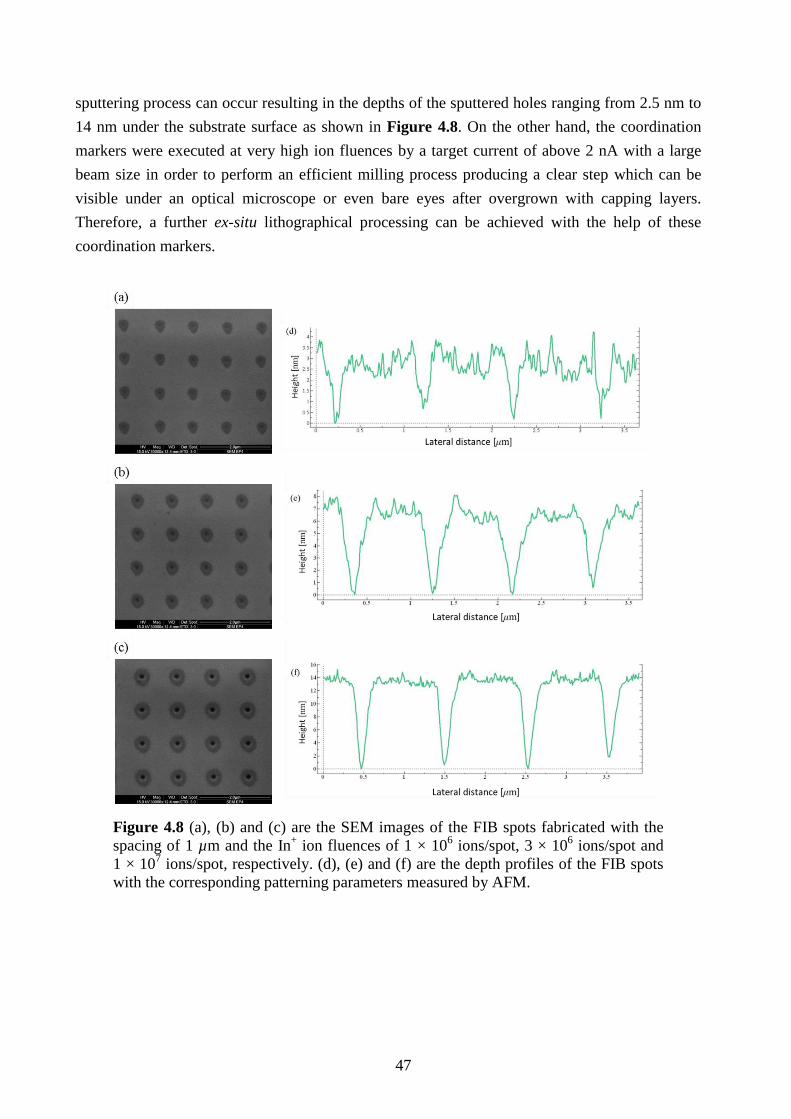
47
sputtering process can occur resulting in the depths of the sputtered holes ranging from 2.5 nm to
14 nm under the substrate surface as shown in Figure 4.8. On the other hand, the coordination
markers were executed at very high ion fluences by a target current of above 2 nA with a large
beam size in order to perform an efficient milling process producing a clear step which can be
visible under an optical microscope or even bare eyes after overgrown with capping layers.
Therefore, a further ex-situ lithographical processing can be achieved with the help of these
coordination markers.
Figure 4.8 (a), (b) and (c) are the SEM images of the FIB spots fabricated with the
spacing of 1 µm and the In+ ion fluences of 1 × 10
6 ions/spot, 3 × 10
6 ions/spot and
1 × 10⁷ ions/spot, respectively. (d), (e) and (f) are the depth profiles of the FIB spots
with the corresponding patterning parameters measured by AFM.

49
Chapter 5 Experimental Details and Characterization
Methods
The experimental details about the sample fabrication and the characterization methods for site-
selected QDs are introduced in this chapter. The fabrication involves the combination of FIB
patterning and MBE growth, where the parameters of FIB patterning have been addressed in the
previous chapter. The essential parameters for the fabrications of self-assembled GaAs nanoholes
and InAs QDs are described in the first section. Two structure characterization techniques, i.e.,
scanning electron microscopy (SEM) and atomic force microscopy (AFM), were employed to
study the topography and morphology of the sample surfaces associated with the nanoholes and
the QDs. The optical characterization of the QDs was obtained from the photoluminescence (PL)
spectra measured by two different techniques, PL spectroscopy and scanning near field optical
microscopy (SNOM).
5.1 Sample Fabrication
As described in section 4.2, the fabrication of the samples includes several processes. The
first step is the growth of an epitaxial GaAs matrix layer with a high purity and a smooth surface
by MBE. The second step is patterning arrays of spots on the sample surface by in-situ FIB
writing. The third one is the formation of GaAs nanoholes by droplet epitaxy in the MBE system.
The last step is the deposition of InAs using different amounts of coverage in order to investigate
the evolution of strain-induced QDs in the GaAs nanoholes by SK growth with MBE. An
illustrated scheme of these processes can be found in Figure 4.2. The MBE growth was executed
by a solid source MBE system of the type Riber Epineat III-V SS. The FIB writing was done by
an Orsay Canion 31 Plus FIB column with a Ga or In LMIS. The experimental setup of these two
systems can be found in section 3.3 and 4.3, respectively. The MBE system is connected with the
FIB column through vacuum valves, i.e., the MBE-FIB system, as illustrated in Figure 3.4. Due
to this advantage, all transport procedures between the processes were performed under UHV
conditions to ensure that the whole fabrication is surface clean.
A quartered 3-inches GaAs (100) epi-ready wafer was first degassed at 150 °C for at least
45 minutes in the load-lock chamber in a vacuum. After degassing, the wafer was transferred into
the growth chamber via the transfer chamber using the transfer rods. Prior to the epitaxial growth,
50
the wafer was thermally cleaned by two steps in the main chamber of the MBE system. First,
the substrate temperature was raised up to Tpyro = 550 °C (Tpyro, pyrometer temperatures) and
maintained for at least 15 minutes to remove the impurities from the substrate in the absence of
arsenic atmosphere. Secondly, the temperature was increased to Tpyro = 600 °C (Tset ~ 660 °C,
depending on the substrate conditions; Tset, thermocouple temperature) to desorb the oxides from
the surface. In order to prevent the dissociation of arsenic from the GaAs substrate, the As valve
has to be opened during the second step. After achieving a stable substrate temperature at 600 °C
and a homogeneous arsenic atmosphere inside the growth chamber with the arsenic BEP, PAs, of
1.3 × 10⁻⁵
Torr, the MBE growth process of the sample fabrication began. It started with the
growth of a 50 nm GaAs epitaxial layer followed by 30 periods of the short-period superlattice
(SPS) with 2 nm AlAs / 2 nm GaAs. The SPS in this case was used to smooth the surface
roughness caused by the impurities from the substrate. From RHEED, a clear reconstruction of
(2×4) along [ ] indicated a smooth GaAs surface. After smoothing, another 150 nm or 200 nm
thick GaAs epilayer was grown as the matrix layer for the subsequent formations of nanoholes
and QDs.
After the growth of a GaAs matrix, the substrate temperature was decreased to a standby
value at Tset = 400 °C. The As valve was then closed and the growth was interrupted to transfer
the sample into the FIB chamber for the process of FIB patterning at room temperature. Two
types of FIB patterns were generated in a sequence. The first one was composed of square arrays
of FIB spots with the variable spacing lspot in an area of 60 × 60 µm2. The second one was made
of a cross-shaped coordination marker. The details about the FIB patterning parameters and the
pattern design can be found in subsection 4.3.3. During the preparation for FIB patterning, the
whole interruption time of growth was about one hour, which includes transferring the sample,
defining the coordination of the sample and fine tuning the ion beam focus, FIB spot patterning
(about 5 minutes for 10 areas) and coordination markers carving (about 30 minutes for 3 markers).
After FIB patterning, the sample was transferred back to the MBE chamber for the generation of
GaAs nanoholes and the deposition of InAs.
During this one hour interruption time, the As valve was fully closed, leading to a decrease
of the background pressure in the growth chamber down to the order of 10-9
Torr. Such low
pressure is essential for the formation of metal droplets during droplet epitaxy. After reloading
the sample in the growth chamber, the substrate temperature was raised up to Tpyro = 545 °C for
the growth in the mode of droplet epitaxy. The deposition of Ga with a nominal coverage θGa of
3 ML or 5 ML was supplied (equivalent to the standard growth of GaAs with the growth rate of
0.70 ML/s calculated by RHEED). During the deposition of Ga, the As BEP was maintained at
around 6.0 × 10⁻⁷
Torr which is the minimum controllable value in the MBE system of this work.
This process is a kind of arsenic-debt atomic layer MBE growth, resulting in the formation of Ga
droplets on the surface by VW growth mode. The slight As pressure could suppress additional
Ostwald ripening during the droplet formation. The nucleation of the deposited Ga atoms on the
FIB-patterned areas was site-selective depending on the arrayed FIB spots, yielding arrayed Ga
metal droplets. Meanwhile, the Ga droplets could be formed on the bare GaAs surface outside the

51
FIB-patterned areas as well, however, in a random distribution. Both of these Ga droplets were
then crystallized by arsenic resulting in GaAs semiconductor nanostructures. With the conditions
of low As pressure and high substrate temperature, a transformation from hemisphere-like
droplets into hole-like nanostructures is favored. The mechanism of nanoholes generated by
droplet epitaxy, including the droplet formation and crystallization, can be found in subsection
3.4.2. The sample was then annealed under the same BEP of As with the temperature rapidly
raised up to Tpyro = 610 °C ~ 620 °C within 2 minutes in order to evaporate the rest of the liquid
Ga droplets [36]. The small amount of As maintained during the annealing process could prevent
possible desorption of As from the crystalline GaAs at this temperature. The fabrication of GaAs
nanoholes was thus achieved. Then, the substrate was cooled down. For the structure
characterization of the GaAs nanoholes, the substrate temperature was cooled down to the
standby temperature, i.e., Tset = 400 °C, for the subsequent ex-situ analyses.
Moreover, GaAs nanoholes formed by droplet epitaxy can be further used as templates for
the site-selective growth of strain-induced QDs. For the overgrowth of these site-selected
QDs after the formation of GaAs nanoholes, the substrate temperature was decreased to
Tpyro = (525 ± 2) °C to allow the deposition of InAs. In meanwhile, the BEP of As was increased
up to 6.8 × 10⁻⁶
Torr for the growth of QDs. The growth rate of InAs was chosen to be
~ 0.04 ML/s in this condition. The total InAs coverage was delivered in consecutive cycles, each
consisting of 4 seconds of In deposition followed by 4 seconds of growth interruption. This
interruption allows the diffusion of In atoms on the surface until they find a suitable location for
binding in order to make up epitaxial layers. The number of In cycles is calculated by using the
RHEED-oscillation data which has previously been gained at a particular substrate temperature.
For the conventional strain-induced QDs grown by the same MBE system of this work, the
standard InAs coverage θInAs is 2.1 ML for InAs QDs grown on a planar GaAs (100) surface.
However, in this work, the InAs coverage θInAs was varied from 1.40 ML to 1.75 ML in order to
study the growth evolution for the site-selectively grown QDs in the GaAs nanoholes. The site-
selected QDs grown in the arrayed GaAs nanoholes on the FIB-patterned areas can follow the
position of the nanoholes, resulting in arrayed QDs. On the other hand, on the bare GaAs surface
outside the FIB-patterned area, the site-selected QDs were reproduced, depending on the
distribution and the density of the GaAs nanoholes, resulting in randomly-distributed QDs.
After the InAs deposition, the sample was either cooled down directly to the standby
temperature and then taken out without capping for ex-situ structure characterization, or the
growth was continued by providing the samples with capping layers to complete the confinement
of QDs for ex-situ optical investigation [1]. The capping layer, an 8 nm or 10 nm GaAs layer, was
grown with the temperature decreased to Tpyro = 510 °C, followed by a 7 nm to 22 nm GaAs layer
growth with the substrate temperature raised to Tpyro = 600 °C. After that, the short period
superlattice with 3 nm AlAs / 1 nm GaAs and/or the GaAs top layer were grown with an arsenic
BEP of 1.3 × 10⁻⁵
Torr. After capping, the sample was cooled down to the standby temperature of
Tset = 400 °C and was then ready for the subsequent ex-situ processes and analyses.

52
In order to define the position of the FIB-patterned areas and also to unite the quantity of the
QDs participating in their ensemble optical properties, an ex-situ photolithography technique was
employed for providing orientation and for segmenting the sample into several regions in terms
of optical measurements. In practical, the quartered 3-inches sample was first cut into a piece of
5 × 5 mm2 including the whole region which has undergone FIB patterning. Then, the square
shaped mesas with an active area of 40 × μm2 were fabricated by photolithography and wet
chemical etching. The alignment of the mesas and the FIB-patterned areas (with the area of
60 × 60 μm2) was achieved by aligning the coordination markers cleaved by FIB with the
markers on the mesa. After etching, an Au metal layer was coated by thermal evaporation in
order to conceal the optical luminescence from the undesired area during the optical measurement.
At the same time, the Au coating layer also makes th m sa structur s com ”visi ”, which
helps for a coarse position tuning in the measurement setups with naked eyes. After these
preparations, the well-defined areas of the sample were ready for the ensemble or single QD
spectroscopy analyses.
Several samples were fabricated with different growth parameters in order to understand the
relation between the structure of GaAs nanoholes and droplet coverage, as well as the growth
evolution of strain-induced QDs in the nanoholes. For the case of nanohole structures, sample A0
and B0 were generated respectively with nominal Ga coverages θGa of 3 ML and 5 ML without
InAs deposition. For the case of InAs QDs in GaAs nanoholes, sample A75 was fabricated with
the GaAs nanoholes formed with θGa of 3 ML followed by the InAs deposition with an InAs
coverage θInAs of 1.75 ML. Also, sample B40, B58 and B75 were fabricated with GaAs nanoholes
formed with θGa of 5 ML followed by InAs deposition with θInAs of 1.40 ML, 1.58 ML and
1.75 ML, respectively. For the optical measurements, the capped samples, C40, C46, C58, C65
and C75, were produced with GaAs nanohole formed with θGa of 5 ML followed by the InAs
deposition with θInAs of 1.40 ML, 1.46 ML, 1.58 ML, 1.65 ML and 1.75 ML, respectively. The
characterization methods used in this work will be introduced in the following sections. The
experimental results of both the randomly-distributed and arrayed GaAs nanoholes will be given
and discussed in Chapter 6, while those of the site-selected InAs QDs grown in both types of
GaAs nanoholes will be shown and discussed in Chapter 7.

53
5.2 Scanning Electron Microscopy
A scanning electron microscope (SEM) is mainly used to observe the topography of a
sample by scanning the surface with a high-energy focused electron beam. The signals derived
from the beam-sample interactions provide the information about external morphology, chemical
composition and the texture of crystalline materials, which can be detected by a variety of
detectors and then converted into images.
All SEMs are essentially composed of a vacuum system, an electron optics column,
detectors and an image processor. The vacuum system generally includes two vacuum chambers
and vacuum pumps. One chamber, which houses the electron optics column, is maintained in
UHV conditions about 1 × 10⁻¹⁰
mbar. Another chamber consists of a sample stage and detectors
usually in a lower vacuum in the order of 10-5
to 10-8
mbar, which is located below the electron
optics column and separated by a valve. The electron optics column is accomplished with the
electron source (gun) and the electromagnetic lenses in order to produce an electron beam with
narrow energy dispersion and precise kinetic energy for scanning the sample. The electron gun is
used to eject electrons by field emission or thermal emission processes. The electromagnetic
lenses include the condenser lenses to condense the electron beam, and the objective lens to focus
the electron beam on the sample surface. After travelling through the electromagnetic lenses, the
accelerated electron beam is incident on the sample. The kinetic energy is dissipated and parts of
this energy result in the ejection of secondary electrons (SE), backscattered electrons, Auger
electrons, X-rays and light. These signals are detected by the appropriate detectors e.g., the
secondary electron detector, the backscatter electron detector, the X-ray detector and the
cathodoluminescence (CL) detector. In an SEM, the secondary electrons provide information of
the morphology and the topography of the sample. The backscattered electrons can be used to
illustrate contrast in composition of multiphase materials. These two signals are the most
commonly used signals for composing SEM images. Furthermore, the X-ray spectra collected for
energy dispersive X-ray spectroscopy (EDX) are characteristic of the atoms, allowing the
chemical composition of the materials to be determined. Finally, the CL spectroscopy collecting
the light emission from the sample has the ability to investigate the optical properties of the
samples.
As in any microscope, the main objective of SEM is for magnification and focus of clarity.
The amount of information which a micrograph can provide is dependent on the resolution of a
microscope. The resolution in a microscope means the smallest interval that one can distinguish
between two adjacent points. With an SEM, the resolution mainly depends on the size of the
electron spot, which in turn depends on the wavelength of electrons and the electron optics
system. When the electron beam enters the lens and aperture system in the microscope, it
produces overlapping diffraction patterns for each point of objects. The distance r between two
diffraction maxima corresponding to the limit of resolution can be determined by:

54
. λ
. λ
sin
where λ is the wavelength of the beam, NA is the numerical aperture, n is the refractive index of
surrounding medium and is the angle between the optical axis and the beam edge. The formula
was developed by E. Abbe [162] and Lord Rayleigh [163] based on light optical microscopes.
For a normal light optical microscope, the maximum resolution is limited to about 200 nm which
corresponds to the wavelength of visible light ranging from 400 nm to 760 nm. However, much
smaller wavelengths can be achieved by using the electron beam in an SEM. The wavelength of
an electron beam can be varied depending on its acceleration voltage, U, with the dependence
derived from the de Broglie relation, λ ⁄ , as given by the formula:
λ
√
where h is Planck’s constant; p is the momentum; me is the electron mass; and e is the electronic
charge. For an electron microscope with the acceleration voltage of 20 kV, the wavelength is
about 0.008 nm which has the potential to increase the resolution by a factor of 104 to 10
5 over
the light optical microscope. When the electron velocity approaches the speed of light, i.e.,
c = 3 × 10¹⁰
cm/s, at a high voltage, e.g., 50 kV, v = 1.326 × 10¹⁰
cm/s, the relativistic correction
of the mass has to be taken into account. However, the maximum resolution is actually not
attainable in SEM because the theoretical wavelength is still limited by lens aberrations,
vibrations, noise and stray fields. The magnification of SEM imaging can range largely to that of
optical microscopy up to a nanometer scale. In a SEM, the magnification is carried out by the
ratio of the dimensions of the raster on a sample and the raster on a display device. Therefore,
unlike light optical microscopes and transmission electron microscopes, where the magnification
is a function of the power of the objective lens, the magnification of SEM is controlled by the
power of scanning coils or deflector. With a fixed display size, higher magnification can be
achieved simply by reducing the size of the raster on the sample.
A Quanta 200 FEG SEM system from FEI has been used for imaging in this work, which is
capable of magnifying from 12× to 1,000,000×. The SEM working with a hot field emission gun
and the acceleration voltage can be operated from 200 V to 30 kV. The maximum resolution in
the high-vacuum mode (~ 6 × 10⁻⁴
Pa) is about 1.2 nm and 3.0 nm at the acceleration voltage of
30 kV and 1 kV, respectively. A SEM has advantages including a high degree of magnification
and an excellent depth of field resulting in its remarkable abilities for imaging a comparatively
large area and showing 3D structure. Moreover, it allows to image bulk materials and not just thin
films or foils, which makes it easy for sample preparation. Owed to the advantages above, SEM
has been considered as a suitable and efficient technique for imaging small 3D nanostructures,
e.g., quantum dots with a great quality. Figure 5.1 shows images with different magnifications by
the Quanta 200 FEG SEM system. The image (a) displays a FIB-sputtered coordination marker
used in this work, while the image (b) illustrates the strain-induced InAs quantum dots on a
planar (100) GaAs surface with a density of the order of 1010
cm-2
grown by the same MBE
system of this work.

55
Figure 5.1 SEM images from the Quanta 200 FEG. (a) A cross-shaped coordination
marker after the growth of droplet epitaxy in MBE, produced by In+ FIB patterning
on a GaAs substrate. (b) The InAs quantum dots grown on the planar (100) GaAs
surface at AFP.
5.3 Atomic Force Microscopy
Atomic force microscopy (AFM) is a scanning probe microscopy technique providing high
resolution topography images on the atomic scale [164]. The working principle is based on
measuring the force between a probing tip and the sample during lateral scanning (x-y). The
sample surfaces can be insulating, semiconducting or conductive, which makes AFM a
complementary technique to scanning tunneling microscope (STM) which is limited to a
conductive or semiconducting sample surface. Moreover, since the measurement can be carried
out in ambient air and no special sample preparation is needed, AFM has been considered as a
versatile and convenient technique to investigate the surface topography of nanostructures made
up of both solid and soft matter.
The key component of an AFM is the cantilever, i.e., a flexible arm, with an atomically
sharp tip set at the end for scanning the sample surface. The cantilevers are usually made of Si
and Si3N4. The small curvature radius of the tip is of the order of nanometers, leading to high
lateral resolution. The working principle of the AFM is illustrated schematically in Figure 5.2 (a).
When the tip is brought into close proximity of the sample surface, the forces between the tip and
the surface will result in a deflection of the cantilever. The relation between the force and the
deflection follows Hook’s law. The potential energy can then be described by
,
where k is the spring constant of the tip of the order of 1 N/m while d is the shortest vertical
displacement. With of the order of 4 × 10-21
J at room temperature, the smallest observable
vertical displacement (z) is 0.5 nm. The force between the tip and the sample is of the order of a
nano Newton [165]. The deflection is monitored by the reflection of an incident laser beam upon
the cantilever into a position sensitive detector which consists of an array of photodiodes. The
output signal from the detector is calculated by normalizing the signal difference between the

56
photodiodes with their sum which is proportional to the total deflection of the cantilever. During
scanning, the force is kept constant by a feedback loop, i.e., keeping a constant distance between
the tip and the surface by moving the cantilever (or the sample) up and down promptly. This
delicate vertical movement can be carried out by piezoelectric actuators which results in a
resolution on the atomic scale. Similar actuators are also used to move the cantilever laterally to
scan a topographic map of the surface features.
The AFM equipment used for this work is a scanning probe microscope from Digital
Instruments equipped with a Si cantilever having a tip with a nominal curvature radius of 5 nm to
10 nm with the angle of 20°. Since the resolution is affected by the tip geometry, the resolution
which can be obtained in this case is in the order of a few nanometers. A tapping mode is
performed to study the surface morphological properties of the samples in order to prevent the
destruction of the surface and the tip as well. In the tapping mode of operation, the tip is
oscillated at its resonant frequency by an actuator. The decrease of the amplitude of the
oscillation generated when the cantilever approaches the sample is used to measure the force
between the tip and the sample [165]. An AFM can provide the information from lateral and
vertical dimensions of the nanostructures present on the sample surface with a high magnification.
Contrary to optical or electron microscopes, e.g., an SEM, which provide a two-dimensional
projection of the surface, AFM can study the information in all three dimensions of the sample.
The resolution of this system is appropriate to study nanostructures such as self-assembled
quantum dots and nanoholes. Figure 5.2 (b) shows an AFM image with the strain-induced InAs
quantum dots grown on a planar (100) GaAs surface by the same MBE system of this work. The
measured base diameter of the dots is about 50 nm while the dot height is around 11.5 nm.
(b)
Figure 5.2 (a) The working principles of AFM. A
sharp tip is mounted on a cantilever for scanning the
surface of the sample. The deflections of the
cantilever are reported by a reflected laser beam into
an array of photodiodes. Photoelectric circuitry of the
detector then converts the deflections into height
information recorded as a digital image [166]. (b)
The AFM topography image of strain-induced InAs
quantum dots grown on a planar GaAs (100) surface.
(courtesy of S. Valentin)

57
However, this method has certain limits which should be taken into account. For example,
AFM characterization requires uncapped quantum dots, while it has been observed that the QD
structural characteristics changes before and after the growth of the capping layer. AFM is
therefore more valuable for a comparative analysis than for quantitative measurement of the QD
dimensions. Furthermore, because the physical resolution is limited by the shape of the tip, the
dimensions of the nanostructures can be distorted by a blunted tip. Also, steep steps normally
cannot be measured because of the nature of AFM tips. Compared to SEM, the size of the AFM
scan image is much smaller in the order of a few tens to hundred micrometers. Moreover, due to
the low scanning speed, the thermal heating of the cantilever by the laser beam can lead to
thermal drift in the image.
5.4 Photoluminescence Spectroscopy
Photoluminescence (PL) spectroscopy is a powerful and non-destructive optical technique
for providing information about the optical properties of semiconductor materials with rapid and
sensitive ability. It is capable of investigating the information involving the intrinsic optical
processes corresponding to host semiconductors, and also the extrinsic optical processes related
to impurities or defects which affect material qualities and device performances [167]. PL
spectroscopy is an efficient technique which has been widely applied for the characterization of
quantum wells, superlattices, and also quantum dots [1].
Photoluminescence is the radiation emitted from semiconductor crystals after the excitation
by an incident light source, e.g., a laser beam. In particular, it reflects the recombination paths of
the photogenerated electron-hole pairs. For example, in a self-assembled quantum dot system, the
electron-hole pairs are obtained by exciting electrons from the valence band (VB) to the
conduction band (CB) using a laser beam with a higher energy than the band gap of the matrix
material, i.e., above-band excitation. In this case, many electron-hole pairs are created in the
matrix surrounding the dot. A fraction of these electrons and holes can be captured by the
quantum dot and then relax nonradiatively to the ground state (s shell) or weakly excited sates
(p, d and f shell) of the quantum dot over a sub-ps-timescale. The electron-hole pairs in the
confined levels of the quantum dot can then recombine radiatively with the typical life time about
1 ns. The radiative recombination is accompanied with the emission of a photon which carries a
characteristic energy. A schematic representation of the photoluminescence process in a quantum
dot is shown in Figure 5.3. A typical PL spectrum from the ensembles of conventional strain-
induced InAs quantum dots embedded in a GaAs matrix is also shown, which was measured at
77 K. The peaks present in the spectrum are associated with the transitions from the s, p and d
shells of the QDs, the wetting layer (WL) and the GaAs. The ground-state transition energy E0 is
about 1.054 eV for the s shell, while the excited-state transition energies E1 and E2 are 1.124 eV

58
and 1.178 eV from the p, and d shells, respectively. The PL spectra of QDs are mainly attributed
to the photon emission following the selection rules which allow the recombination of the
electrons and the holes belonging to the levels of same quantum numbers and whose
wavefunctions are sufficiently overlapped [168]. In other words, an electron in an s shell will
recombine with a hole in the s shell, a p electron with a p hole, and so on. When the temperature
is low enough such that kBT is smaller than the quantum dot energy level spacing, the quantized
properties of the energy levels become apparent in the PL spectra. The number of the electron-
hole pairs present in the system can be adjusted by the excitation power density. Since the
relaxation times to the ground states are much shorter than the life-time of the radiative
recombination, the emission from the s shell can be observed at a low excitation power. As the
excitation power density is increased, more carriers are present in the QD system and the higher
shells are filled subsequently. This phenomenon is known as level-filling represented as the
typical behavior of self-assembled InAs QDs [53]. More information can be obtained by
analyzing the luminescence spectrum as a function of different parameters, e.g., temperature and
excitation wavelength.
(a) (b)
Figure 5.3 (a) The schematic illustration of the photoluminescence processes (1) to (4) for a self-
assembled InAs/GaAs QD system (adapted from [104]). (1) the formation of electron-hole pairs
in the GaAs bulk by a laser excitation (2) the capture of the carriers into the QD (3) the relaxation
to the ground state (e1 for electrons; hh1 for heavy holes, corresponding to the s shell of the QD),
or to the lowest unoccupied excited state (e2 and e3; hh2 and hh3, corresponding to the p and d
shells of the QD, respectively) (4) the recombination with the emission of photons carrying
characteristic energies E0, E1 and E2 from the transition of s, p, and d shells, respectively.
(b) A typical PL spectrum measured at 77 K from the ensembles of conventional strain-induced
InAs QDs in a GaAs matrix grown by the same MBE system of this work at AFP (provided by
A. Rai). The PL peaks are attributed to the transitions of the discrete energy states, s, p and d
shells, of the QDs. The transition peaks of the InAs wetting layer (WL) and the GaAs are also
present.

59
Figure 5.4 shows a schematic for the experimental apparatus of the PL setup used for
measuring the optical properties from the ensembles of QDs in this work. The excitation source is
a diode laser with a wavelength of 635 nm, i.e., 1.95 eV, operating with an excitation power of
5 mW. The energy of the laser is higher than the band gap of the semiconductor under study, e.g.,
~ 1.51 eV for GaAs at 77 K. The samples are fixed on a finger cryostat for low temperature
measurements. The cryostat is capable of cooling down to 4.2 K. A resistance thermometer, i.e., a
PT 100 resistor, is capable of measuring the temperature from room temperature down to 70 K.
An Allen-Bradley resistor is used for measuring temperatures down to 4 K. The cryostat is
equipped with a high purity quartz window, which allows the excitation as well as the
luminescence light to pass through. The cryostat is mounted on a movable table which allows
sample movement in all three dimensions in order to make an intersection of the laser beam and
the optical axis and also to realize sample mapping. The associated optics includes a mirror and a
lens to reflect and focus the excitation light to a small spot in the order of 10-5
cm2 on the sample,
and two other lenses to focus the luminescence signals on the entrance slit to a high resolution
monochromator. A SPEX 500M monochromator is capable of dispersing the luminescence
signals spectrally by a diffraction grating with a blaze optimized to a wavelength of 750 nm or
1000 nm. The dispersed signals are then detected by a LN2-cooled InGaAs detector with a lock-in
amplifier measuring the detector signal in modulating the frequency of the laser with 133 Hz in
“internal oscillator made” to bandpass-filter the signal for noise suppression. Finally, the signal
from the lock-in amplifier is digitally read out with the help of an IEEE-488 interface and a
Lab-View computer program which is also used to control the monochromator and also for data
processing and storage.
In contrary to the PL spectroscopy, a scanning near field optical microscope (SNOM) is used
to distinguish the single QDs both spectrally and spatially. Because of the sub-wavelength
aperture diameter of the probe, the resolution limit of a typical optical microscope can be
overcome with this technique which results in high resolution images [165, 169, 170]. A
schematic illustration is shown in Figure 5.5 with the layout of the aperture-type SNOM at
Max Planck Institute (MPI) of Microstructure Physics, Halle. The microscope setup is mounted
inside a vacuum chamber under ultra-high vacuum conditions. The sample is attached to the cold
finger of a cryostat which is capable of stabilizing the temperature in the range between 8 K and
300 K by a liquid helium flow. The SNOM scan head consists of a near-field fiber probe, a tuning
fork shear-force setup to regulate the distance between the probe and the sample surface,
piezoelectric actuators for fine positioning on a nanometer scale, and a motorized translation
stage for coarse positioning on a micrometer scale. The near-field fiber probe is made by pulling
an optical fiber to a sharp tip modified from an AFM tip with a thin metal coating layer and an
aperture with a diameter of about 300 nm at the end of the tip. The fiber tip is glued along one
side of the arms of the quartz crystal tuning fork. The distance between the sample and the tip is
kept very small by the use of a feedback mechanism based on the regulation of the quartz tuning
fork. The sample or the tip is scanned so as to construct an image of the sample. A microscope
objective allows for visual inspection of the tip-sample region by collecting the reflected light

60
from the illumination with an LED. The light is then routed onto a camera outside the vacuum
chamber. The microscope objective can also be used for far-field illumination and illumination
collection of the sample. A green He-Ne laser source with the wavelength of 543 nm is coupled
to the SNOM via an optica fi r coupler. In spectroscopic experiments, the luminescence emitted
from the sample is also guided by the optical fiber and then spectrally dispersed in a
monochromator SP2560 on the grating of 150 lines/mm with a blaze optimized for a wavelength
of 800 nm and a slit width of 150 μm, and finally detected by an InGaAs detector.
Figure 5.4 The experimental setup for the PL spectroscopy with a laser diode at the
wavelength of 635 nm, the lenses and a mirror, a monochromator, a LN2-cooled
InGaAs photodetector, a lock-in amplifier and the computer control unit. (adapted
from [104])
Figure 5.5 Schematic diagram of the SNOM setup at Max Planck Institute of
Microstructure Physics, Halle. (courtesy of A. Senichev)

61
Chapter 6 Characterizations of Self-assembled/Self-
patterned GaAs Nanoholes
Site-control has been considered as a promising pathway to integrate self-assembled QDs into
single QD based devices for the implementation of solid-state quantum information. In this work,
the site-control was realized by using self-assembled/self-patterned GaAs nanoholes as templates
for the subsequent site-selective growth of QDs by MBE. To study the properties of these site-
selected QDs formed on the nanohole templates, it is important to first understand the structures
of the nanoholes which may influence the performance of the quantum systems directly. The self-
assembled/self-patterned GaAs nanoholes of this work were generated by droplet epitaxy. In
order to study the influence of the Ga coverage on the topography of nanoholes, two different
amounts were applied. For each sample, the GaAs nanoholes were formed on the bare GaAs
surface (without FIB pre-patterning) and also on the FIB-modified surface, i.e., the FIB-patterned
areas. The FIB-patterned areas composed of square arrays of FIB spots were created by an in-situ
FIB technique with different patterning parameters on a GaAs surface. In this chapter, the
characteristics of the GaAs nanoholes formed on both types of surfaces are shown and discussed
in two subsequent sections. In the first section, the nanoholes on the bare GaAs surface are
addressed with their shapes and distributions. Then, the impact of FIB patterning on the
arrangements and the structures of the nanoholes is discussed in the second section with several
different FIB-patterned areas. A comparison between the GaAs nanoholes on the bare GaAs
surface and on the FIB-patterned area is also included.
6.1 Randomly-distributed Nanoholes
For the site-selective growth of QDs with surface-patterned templates, the geometry of the
templates is one of decisive parameters leading to the preferential nucleation of the overgrown
materials. For GaAs nanostructures generated by droplet epitaxy, the morphology depends on the
diffusion region of Ga atoms or GaAs molecules (before being solidified into GaAs crystals)
together with initial preferential nucleation at the skirts of Ga droplets. The preferential
nucleation at the skirt is driven by the surface energy difference of three phases. The diffusion
region is determined by the competition between Ga atomic migration and As incorporation
[115, 116]. Meanwhile, high substrate temperatures can lead to thermal melting of liquid Ga
droplets resulting in local concaves on the surface [36, 39, 114]. Therefore, the shape of the

62
nanoholes is mainly influenced by substrate temperature, arsenic pressure and the size of metal
droplets [27, 28, 113]. In order to optimize the structures of nanoholes for the site-selective
growth of QDs, two GaAs nanohole samples, A0 and B0, were fabricated with nominal Ga
coverages θGa of 3 ML and 5 ML, respectively, at high temperature and low As pressure by
droplet epitaxy. For studying the morphology of these nanoholes, no InAs was deposited on the
samples. The details about the sample fabrications are described in section 5.1. These two GaAs
nanohole samples were characterized by SEM and AFM for a full inspection of the
nanostructures.
Figure 6.1 The GaAs nanoholes on the bare
GaAs surface of sample A0 fabricated with
θGa = 3 ML by droplet epitaxy. (a) The SEM
image (30,000×) (b) The AFM 3D topography
of a typical nanohole with the lateral distances
of x along [ ] and y along [ ], and the
height, z. (c) The profiles corresponding to the
AFM topography. L is the outer diameter of the
nanohole. l is the diameter of the wall. H and h
are the (higher and lower) heights of the wall
along x or y. is the inner width of the
nanohole with respect to the half maximum of h
along the corresponding direction. The red
horizontal dotted line corresponds to the
substrate surface, while the black one to the
bottom of the hole.
Figure 6.1 presents the SEM image of GaAs nanoholes formed on sample A0 with a
nominal Ga coverage of 3 ML and the AFM topography of one typical GaAs nanohole on this
sample. These self-assembled GaAs nanoholes are randomly-distributed on the GaAs surface
with a density of ~ 8.0 × 107 cm
-2. In the SEM image (a), the nanoholes represent an inner

63
diameter of ~ 25 nm along the crystal direction of [ ]. In the AFM 3D image (b), the typical
GaAs nanohole has an asymmetric wall elongated along [ ] which surrounds the inner hole. In
droplet epitaxy, this kind of walls from the nanoholes is also known as a ring-like structure which
is usually transformed from a droplet crystallized with low arsenic pressure. The formation of a
ring-like structure is due to a faster solidification rate at the edge of a metal droplet resulting from
preferential nucleation at the interface of three phases which starts at the skirt of the droplet [115]
and a downhill material transportation from the droplet by diffusion [29, 31]. Because the atomic
diffusion rates depend on the crystal directions of the substrate, the differences of the material
transportations toward different directions lead to the asymmetric structure of the nanohole. The
profiles in (c) corresponding to the cross-sections of the typical GaAs nanohole along [ ] and
[ ] directions feature the dimensions which are denoted as follows. The outer diameter of the
whole nanohole structure is indicated as L. The diameter of the wall surrounding the inner hole is
labeled as l measured from the tops of the wall. The heights of the wall along each crystal
direction are indicated as H and h for the higher and lower ones, respectively. The inner width of
the nanohole, represented by , is measured at the half maximum of the lower height h along a
corresponding direction. The average values of these dimensions measured by AFM from sample
A0 are listed in Table 6.1 for [ ] and [ ] directions, respectively.
θGa = 3 ML L l H H
[ ] 315 ± 15 127 ± 5 2.1 ± 0.3 0.9 ± 0.3 33 ± 6
[ ] 240 ± 13 106 ± 10 1.1 ± 0.2 0.9 ± 0.1 45 ± 9
Table 6.1 The dimensions of GaAs nanoholes on the bare GaAs surface of sample A0
along [ ] and [ ] directions in units of nanometers. The nanoholes were formed with a
nominal Ga coverage of 3 ML. L is the outer diameter of the nanohole. l is the diameter of
the wall. H (higher) and h (lower) are the heights of the wall. is the inner width of the
nanohole with respect to the half maximum of h.
Because of the faster crystal growth at the edge of droplets and the initial preferential
nucleation occurring at the skirts [29, 31], the diameter of walls l and the heights of walls, H and
h, are suggested to be dependent on the dimensions of the original metal droplets [32]. Moreover,
the outer diameter of the nanoholes L depends on the diffusion region of Ga atoms or GaAs
molecules which is determined by the substrate temperature and the As pressure during
crystallization [32]. From the ratio of the outer diameters of nanoholes between two directions,
, which is about 1.3, a faster atomic migration along [ ] is substantiated compared
to [ ]. This ratio is slightly larger than the ratio for the diameters of the walls with
corresponding directions, , which is about 1.2. Meanwhile, the outer diameters of
nanoholes are more than twice larger than the diameters of walls for each direction. These results
all validate a significant lateral diffusion of atoms or molecules from droplets under this growth
condition. Moreover, the wall of a nanohole has different heights along the direction of [ ]
with a ratio of about 2 by . This height difference reveals an asymmetrical atomic

64
migration along this direction, i.e., different diffusion rates towards two opposite orientations of
[ ] and [ ]. The lower side of the wall was proposed to be originated along the direction
with a faster Ga diffusion rate [32]. However, the heights of the wall along another direction, i.e.,
[ ], are nearly equivalent. These observations suggest that the asymmetrical atomic migration
is more pronounced in the direction with a faster atomic diffusion, i.e., [ ]. It is noticed that
although the whole nanohole structure is larger in the lateral dimension along [ ], the inner
width of the nanohole is wider along [ ] with a ratio of about 1.4 by . For
convenience, GaAs nanoholes formed with a nominal Ga coverage of 3 ML on a bare GaAs
surface are simplified as A-type nanoholes in the following.
Figure 6.2 The GaAs nanoholes on the bare
GaAs surface of sample B0 fabricated with
θGa = 5 ML by droplet epitaxy. (a) The SEM
image (30,000×) (b) The AFM 3D topography
of a typical nanohole with the height of z and the
lateral distances of x and y along [ ] and
[ ], respectively (c) The profiles of the typical
nanohole corresponding to the AFM topography.
L is the outer diameter of the nanohole. l is the
diameter of the wall. H and h are the (higher and
lower) heights of the wall along one direction.
is the inner width of the nanohole with respect to
the half maximum of h along the corresponding
direction. The red horizontal dotted line relates
to the substrate surface, and the black one to the
bottom of the hole.
Figure 6.2 shows the SEM and the AFM image of GaAs nanoholes on sample B0 which was
fabricated with a nominal Ga coverage of 5 ML. Compared with those of sample A0, these GaAs
nanoholes on the bare GaAs surface of sample B0 are also randomly distributed, but with a

65
slightly lower density of 7.0 × 107 cm
-2. This reduction of density along with an increase of Ga
coverage can be proposed as the evidence of Ostwald ripening involved in the formation of metal
droplets. In the SEM image (a), the nanoholes have an inner diameter of about 33 nm along the
crystal direction of [ ]. An asymmetric ring-like structure surrounding the inner hole is
observed with a higher brightness in the image. This ring-like structure corresponds to the wall
structure shown in the AFM image (b) which illustrates the topography of a typical GaAs
nanohole of this sample. As mentioned earlier, the lateral asymmetric structure of the wall was
caused by the difference of atomic migration between [ ] and [ ] directions. The topography
of this typical nanohole is similar to that on sample A0. However, with sample B0, the wall of the
nanohole can be viewed as an integration of two adjacent hills with different heights. The
difference of the heights is due to asymmetric atomic migration along opposite crystal directions.
These two hills are represented as the asymmetric peaks in the profile (c) according to the cross-
sections of the nanohole along [ ] and [ ]. Especially for the direction of ], the higher
hill has a higher degree of asymmetry than the lower one. The designated dimensions of the
nanohole are illustrated in the profile in the way similar to those of the A-type nanoholes on
sample A0. As a matter of convenience, GaAs nanoholes formed with a nominal Ga coverage of
5 ML on a bare GaAs surface are simplified as B-type nanoholes in the following. In Table 6.2,
the average values of the dimensions of the B-type nanoholes on sample B0 are listed with both
[ ] and [ ] directions.
θGa = 5 ML L l H h
[ ] 321 ± 19 143 ± 10 4.2 ± 0.4 2.9 ± 0.5 34 ± 8
[ ] 222 ± 7 127 ± 9 2.3 ± 0.5 2.0 ± 0.4 60 ± 11
Table 6.2 The dimensions of GaAs nanoholes on the bare GaAs surface of sample B0
along [ ] and [ ] directions in units of nanometers. The nanoholes were formed with a
nominal Ga coverage of 5 ML. L is the outer diameter of the nanohole. l is the diameter of
the wall. H (higher) and h (lower) are the heights of the wall. is the inner width of the
nanohole with respect to the half maximum of h.
Due to a larger Ga atomic migration along [ ] than along [ ], the B-type nanoholes of
sample B0 are represented with an elongated outer diameter which is similar to the A-type
nanoholes of sample A0. However, unlike the A-type nanoholes, the asymmetric heights of walls
are present not only along [ ] but also along [ ] for the B-type nanoholes. The ratio of the
heights, H to h, is about 1.4 along [ ], and 1.2 along [ ]. This reveals that the asymmetric
atomic diffusions in these two directions are both significant under the growth conditions of this
sample. The diameters of the walls along these two directions for the B-type nanoholes are larger
than those along corresponding directions for the A-type nanoholes, respectively. Since the
diameters of walls depend on the size of original droplets, the walls with broader diameters can
be suggested as the productions transformed from larger droplets generated with a higher material
supply by VW growth [113]. Compared with those of the A-type nanoholes along corresponding

66
directions, the wall heights, H and h, of the B-type nanoholes generated with a higher Ga
coverage are more than twice higher, respectively. It has been found that a larger droplet
consisting of a longer interface area (the skirt of a droplet) can result in a stronger crystallization
leading to an increase of wall heights [32]. These results concerning the dimensions are all
consistent with the relation that larger droplets lead to broader nanoholes together with higher and
wider walls. However, the ratio of two heights along [ ], , decreased from 2 to 1.4,
as the Ga coverage increased from 3 ML to 5 ML. In other words, these two hills of the walls
both become higher with an increase of Ga coverage, but the contrast between them becomes
smaller. Compared with the A-type nanoholes, the B-type nanoholes have a larger outer diameter
along [ ], but a slightly shorter outer diameter along [ ], resulting in a higher ratio of 1.4 by
. In these growth conditions, the outer diameters of the nanoholes are determined by
the atomic diffusion along with a downhill material transportation. Therefore, it can be assumed
that the paths for the material to reach the surface are longer in the case of larger and higher
droplets generated by a higher Ga coverage. With the direction of [ ] displaying a slower
diffusion rate, the material supply for growing the outer diameters of nanoholes might thus be
less sufficient, resulting in the smaller outer diameters. Finally, compared with those of the
A-type nanoholes, the widths of the B-type nanoholes are generally wider together with a larger
ratio of .
Concluding this section, self-assembled/self-patterned GaAs nanoholes were successfully
fabricated under the conditions of low As pressure and high substrate temperature by droplet
epitaxy. These nanoholes are constructed by the asymmetric walls surrounding the inner holes
with the bottoms slightly below the sample surface due to thermal etching. These kinds of
structures are generally referred to as ring-like structures or holed nanostructures represented as
valleys [33]. The asymmetry structures result from the different atomic diffusion rates along the
different crystal directions of the substrate. Due to a fast crystal growth at the edge of droplets
and a downhill material transport, higher and broader walls can be transformed from larger Ga
droplets which are formed with a higher Ga coverage [42]. According to the experimental results,
Figure 6.3 shows two similar proportional relations between the wall heights, , and the wall
diameter, , along [ ] for the A-type and the B-type nanoholes formed with nominal Ga
coverages of 3 ML or 5 ML, respectively. These nanoholes are composed of high densities of
monolayer steps (high-index surface) which can be the preferential nucleation sites for the
overgrowth of QDs. Compared to the A-type nanoholes, the B-type nanoholes with a larger
valley which is wider along the crystal direction of [ ] have a broader field of preferential
nucleation sites. With ideal surface-patterned templates for site-selective growth, the densities of
overgrown QDs should be consistent with those of patterned nanoholes. Here, the densities of
these two types of self-patterned nanoholes are both less than one nanohole per µm2. This value is
suitable for the study of single nanostructure spectroscopy which is useful to realize the
properties of individual quantum dots for single QD devices.

67
Figure 6.3 The plot with the higher
heights of the walls H as a function of
the diameters of the walls l along for the GaAs nanoholes on the bare
GaAs surfaces of sample A0 and B0
fabricated with nominal Ga coverages
of 3 ML and 5 ML, respectively.
6.2 Arrayed Nanoholes
In the previous section, the GaAs nanoholes formed on the bare GaAs surface of sample A0
and B0 by droplet epitaxy have been represented with a random distribution. At the same time,
the GaAs nanoholes were also formed on the FIB-patterned areas of these two samples. These
FIB-patterned areas were created by an In+ or Ga
+ ion beam with an ion energy of 30 keV. Each
FIB-patterned area was composed of square arrays of FIB spots within an area of 60 × 60 µm2.
For different FIB-patterned areas, the ion fluence of the FIB spots, Φion where ion denotes In or
Ga, was varied from 3 × 10⁴ ions/spot to 1 × 10
7 ions/spot, while the spacing between the FIB
spots (the pitch), lspot, was designed as 0.5 µm, 1 µm or 2 µm. The details about FIB parameters
and pattern designs can be found in subsection 4.3.3.
For sample B0, the Ga+ ion beam was employed for pre-patterning before the formation of
GaAs nanoholes by droplet epitaxy. Figure 6.4 and Figure 6.5 show the SEM images of self-
assembled GaAs nanoholes formed on the FIB-patterned areas composed of square arrays of FIB
spots with different spot spacings (only a part of each FIB-patterned area is shown). The Ga+ ion
fluences ΦGa are varied from 3 × 10⁴ ions/spot to 3 × 10
6 ions/spot for different FIB-patterned
areas. As shown in Figure 6.4 with a spot spacing of 2 µm, the GaAs nanoholes are not arranged
by the FIB spots and represent a random distribution on the surface with the lowest Ga+ ion
fluence of 3 × 10⁴ ions/spot (a). With Ga
+ ion fluences above 1 × 10
5 ions/spot, the GaAs
nanoholes were formed preferentially and well-organized by the square arrays of FIB spots.
These results reveal the limit of Ga+ ion fluence for ordering the GaAs nanoholes with a
minimum of 1 × 10⁵ ions/spot at these conditions. With the Ga
+ ion fluence of 1 × 10
5 ions/spot
(b), each FIB spot is occupied by one GaAs nanohole, i.e., a single nanohole. For the higher Ga+
ion fluences of 3 × 10⁵ ions/spot (c) and 1 × 10
6 ions/spot (d), there are one or two GaAs
nanoholes present in one FIB spot, i.e., single or double nanoholes. With an even higher Ga+ ion

68
fluence of 3 × 10⁶ ions/spot (e), triple nanoholes are observed. In other words, the amount of
GaAs nanoholes can be increased to exceed the number of the FIB spots, as long as the ion
fluence is sufficiently high. However, with the highest Ga+ ion fluence of 3 × 10
6 ions/spot, the
GaAs nanoholes tended to form at the edges of the FIB spots instead of the center.
Figure 6.4 The FIB-patterned areas of
sample B0 with the spot spacing of
2 µm and different Ga+ ion fluences of
(a) 3 × 10⁴ ions/spot,
(b) 1 × 10⁵ ions/spot,
(c) 3 × 10⁵ ions/spot,
(d) 1 × 10⁶ ions/spot, and
(e) 3 × 10⁶ ions/spot.

69
Figure 6.5 The FIB-patterned areas of sample B0 with different Ga+ ion fluences ΦGa
and spot spacings lspot. (a) lspot = 0.5 µm and ΦGa = 3 × 10⁵ ions/spot, (b) lspot = 1 µm and
ΦGa = 1 × 10⁵ ions/spot, (c) lspot = 1 µm and ΦGa = 3 × 10
5 ions/spot, and (d) lspot = 1 µm
and ΦGa = 1 × 10⁶ ions/spot.
With smaller spot spacings of 0.5 µm and 1 µm, the preferential formation of self-assembled
GaAs nanoholes on the FIB spots occurred as well, as shown in Figure 6.5. However, not all the
FIB spots lead to the formation of GaAs nanoholes. For the FIB spots occupied with GaAs
nanoholes, the nanoholes are present in a single or double form on each FIB spot. Similar to the
results observed from the FIB-patterned areas with the spacing of 2 µm, the increase of the GaAs
nanoholes and the displacement of the location from the center of the FIB spots are also observed
with the increasing ion fluence for the areas with the spacing of 1 µm. With the smallest spot
spacing of 0.5 µm, the GaAs nanoholes become less-ordered, although the Ga+ ion fluence is
above the limit value of 3 × 10⁵ ions/spot. This random-like distribution of GaAs nanoholes
indicates that the spot spacing of 0.5 µm is too close for performing a good alignment of the
nanoholes at this condition. Therefore, controlling the spacing between the FIB spots is one of the
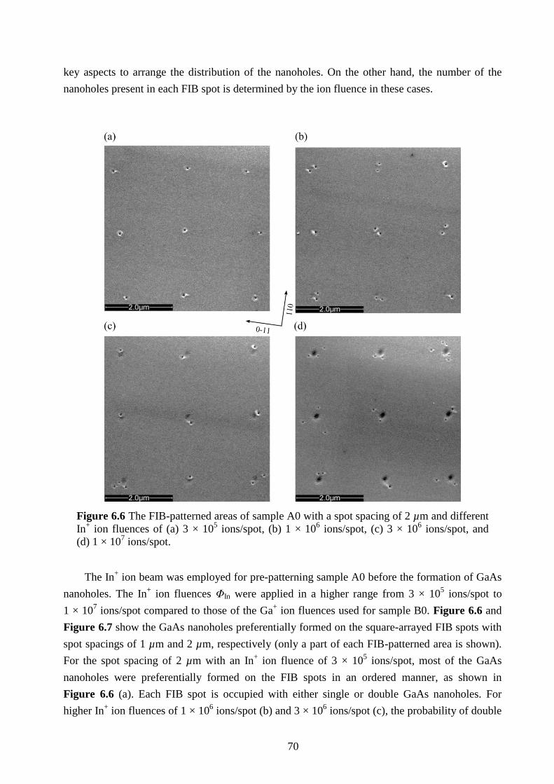
70
key aspects to arrange the distribution of the nanoholes. On the other hand, the number of the
nanoholes present in each FIB spot is determined by the ion fluence in these cases.
Figure 6.6 The FIB-patterned areas of sample A0 with a spot spacing of 2 µm and different
In+ ion fluences of (a) 3 × 10
5 ions/spot, (b) 1 × 10
6 ions/spot, (c) 3 × 10
6 ions/spot, and
(d) 1 × 10⁷ ions/spot.
The In+ ion beam was employed for pre-patterning sample A0 before the formation of GaAs
nanoholes. The In+ ion fluences ΦIn were applied in a higher range from 3 × 10
5 ions/spot to
1 × 10⁷ ions/spot compared to those of the Ga
+ ion fluences used for sample B0. Figure 6.6 and
Figure 6.7 show the GaAs nanoholes preferentially formed on the square-arrayed FIB spots with
spot spacings of 1 µm and 2 µm, respectively (only a part of each FIB-patterned area is shown).
For the spot spacing of 2 µm with an In+ ion fluence of 3 × 10
5 ions/spot, most of the GaAs
nanoholes were preferentially formed on the FIB spots in an ordered manner, as shown in
Figure 6.6 (a). Each FIB spot is occupied with either single or double GaAs nanoholes. For
higher In+ ion fluences of 1 × 10
6 ions/spot (b) and 3 × 10
6 ions/spot (c), the probability of double

71
GaAs nanoholes becomes higher. Furthermore, with the In+ ion fluence of 3 × 10
6 ions/spot, there
are triple or even quadruple nanoholes present in one FIB spot. However, as the ion fluence
increased, the location of the GaAs nanoholes shifted from the center towards the edges of the
FIB spots. These observations are similar to the results of sample B0 patterned by the Ga+ ion
beam. Finally, with the highest In+ ion fluence of 1 × 10
7 ions/spot (d), multiple GaAs nanoholes
are located not only at the edges of FIB spots but also at the positions further away from the spots.
However, because the spot spacing of 2 µm is larger than the displacement, the arrangement of
the GaAs nanoholes is still distinguishable, which is dependent on the FIB pattern.
Figure 6.7 The FIB-patterned areas of sample A0 with a spot spacing of 1 µm and different
In+ ion fluences of (a) 3 × 10
5 ions/spot, (b) 1 × 10
6 ions/spot, (c) 3 × 10
6 ions/spot, and
(d) 1 × 10⁷ ions/spot.
With the spot spacing of 1µm and the In+ ion fluence of 3 × 10
5 ions/spot, the nucleation of
GaAs nanoholes was well located on the FIB spots, as shown in Figure 6.7 (a). Similar to the
results of Ga+ ion patterning with corresponding parameters on sample B0, not every FIB spot

72
exhibits the formation of GaAs nanoholes. With the higher In+ ion fluences of 1 × 10
6 ions/spot
(b) and 3 × 10⁶ ions/spot (c), single or double GaAs nanoholes are present on each occupied FIB
spot. Even though there are still empty FIB spots, the probability of double GaAs nanoholes
increases with the increasing ion fluence. The displacement of the nucleation location relative to
the center of the FIB spots is also observed with high ion fluences. For the highest In+ ion fluence
of 1 × 10⁷ ions/spot (d), the amount of the occupied FIB spots decreases significantly, although
the amount of the GaAs nanoholes increases. In other words, the preferential formation of the
GaAs nanoholes at the FIB spots is no longer favored. Furthermore, the location of the GaAs
nanoholes occurred at the edges and also between the FIB spots, resulting in a random
distribution. This result reveals the limit of In+ ion patterning for positioning self-assembled
GaAs nanoholes at the ion fluence around 3 × 10⁶ ions/spot and the spot spacing of 1 µm.
As described in subsection 4.3.2, a focused ion beam is typically composed of a core and a
long-range tail. The ion current intensity of the ion beam is much smaller at the tail than that at
the center with at least two orders of magnitude lower than the peak intensity [146, 158, 159].
The range of the tail can vary in a range of a few µm [160]. Thus, for the FIB writing process of
spot arrays with a high ion current density, the exposed areas are in a much wider region beyond
the size of the FIB spots. Therefore, an unintentional exposure is created with the ion
concentration decreasing with the distance from the center of the FIB spots [171]. From the
experimental results above, it can be deduced that the Ga adatoms were drawn to the FIB spots
and then preferentially nucleated at the sites containing sufficient surface chemical potential
gradients induced by FIB sputtering and a certain ion concentration C0. In the cases of this work,
either by Ga+ or In
+ beams, single GaAs nanoholes were formed at the center of the FIB spots
with the ion fluences of 1 × 10⁵
ions/spot and 3 × 10⁵ ions/spot. This suggests that the surface
chemical potential gradients were only sufficient at the center along with the ion concentration of
C0 with these cases. When the ion fluence further increased, the preferential nucleation became
unfavorable at the center of the FIB spots, but took place at the position away from the center
where the ion concentration was much lower due to the exposure from the beam tail. Because the
ion current density decreases monotonically with the distance from the beam center, ion beams
with higher ion current densities can create broader circular regions featured with C0, providing
more preferential nucleation sites for the overgrown Ga droplets by droplet epitaxy. Multiple
GaAs nanoholes crystalized from the droplets were therefore generated together with the
displacement from the center of FIB spots.
However, the arrangement of the GaAs nanoholes can become disordered if the ion fluence
is too high. Also, the ion fluence can be integrated if the spot spacing is as small as the range of
the beam tail, resulting in an undesired high ion concentration between the spots. As a result, FIB
pre-patterning can loose the function of positioning self-assembled GaAs nanoholes. In order to
achieve the alignment of the GaAs nanoholes with a high accuracy, it is necessary to maintain a
regular ion concentration profile on the substrate surface by controlling ion fluence and spot
spacing. Furthermore, with an ion fluence above 1 × 10⁶ ions/spot, a strong sputtering process
can lead to damages of the substrate, resulting in sputtered holes with the depth in the order of

73
nanometers as shown in subsection 4.3.3. These sputtered holes remaining on the surface may
affect the crystal qualities, resulting in the reduction of the optical properties. Therefore, the
selection with a low but sufficient ion fluence is required to produce arrayed nanohole templates
for overgrown site-selected quantum structures, e.g., QDs, and to ensure the optical or electrical
performance of the quantum systems as well. In this work, the optimum parameters of FIB
patterning are found to be an ion fluence of 3 × 10⁵ ions/spot and a spot spacing of 2 µm for the
positioning of GaAs nanoholes formed by droplet epitaxy. Comparing In+ and Ga
+ ion patterning
regarding to the distribution of GaAs nanoholes of sample A0 and B0, similar results are found
with the corresponding FIB parameters of ion fluences from 3 × 10⁵ ions/spot to 3 × 10
6 ions/spot
and spot spacings of 1 µm and 2 µm. Therefore, it can be concluded that In+ and Ga
+ ion beams
have the comparable abilities for controlling the sites of self-assembled GaAs nanoholes under
these conditions.
From the above results, the number of GaAs nanoholes in each FIB spot depends on the ion
fluence ranging from 1 × 10⁵ ions/spot to 3 × 10
7 ions/spot, resulting in single, double or multiple
nanoholes. To summarize, the probabilities1 of single, double and multiple GaAs nanoholes are
registered as rn, where n is the amount of nanoholes in one FIB spot. Therefore, r1, r2, r3··· are the
probabilities of single, double, triple… nanoholes. The sum of these nanohole probabilities is
then equal to the occupancy rate of the FIB spots, rsum = r1 + r2 + r3 +···. Figure 6.8 (a) shows rn
as a function of n and the value of rsum with different ion fluences applied on the FIB-patterned
areas of sample B0 with a spot spacing of 2 µm by Ga+ ion patterning. Increasing the Ga
+ ion
fluence from 1 × 10⁵ ions/spot to 3 × 10
6 ions/spot, the probability of single nanoholes r1 is
dominated along with an increase of the probability of double nanoholes r2. At the same time, the
occupancy rate rsum increases from 87 % to 97 %. Similar results are also observed for the FIB-
patterned areas of sample A0 generated by In+ ion patterning with spot spacings of 2 µm and
1 µm and different ion fluences, as shown in Figure 6.8 (b) and (c). With the spacing of 1 µm,
the occupancy rate rsum increases from 59 % to 82 % with the increase of In+ ion fluence, while
with the spacing of 2 µm, it is nearly 100 % for all the range of the ion fluence except
3 × 10⁶ ions/spot. Furthermore, with the spacing of 2 µm, when the In
+ ion fluences are high at
1 × 10⁷ ions/spot and 3 × 10
7 ions/spot, the probabilities of double and triple nanoholes, r2 and r3,
become dominant in sequence. With corresponding FIB patterning parameters, the occupancy
rate rsum for sample A0 with In+ ion patterning is found higher than that for sample B0 with Ga
+
ion patterning. Therefore, In+ ion patterning can be considered more reliable than Ga
+ ion
patterning in terms of representing a higher probability of the occurrence of GaAs nanoholes in
these conditions.
1 The probability is calculated by the amount of the FIB spots occupied by single, double or multiple GaAs
nanoholes divided by the total amount of the patterned FIB spots. The calculation was done with the SEM
images showing larger fields of the FIB-patterned areas with smaller magnification than the images shown in
this thesis.
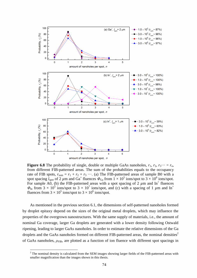
74
Figure 6.8 The probability of single, double or multiple GaAs nanoholes, r1, r2, r3··· = rn,
from different FIB-patterned areas. The sum of the probabilities equals to the occupancy
rate of FIB spots, rsum = r1 + r2 + r3 ···. (a) The FIB-patterned areas of sample B0 with a
spot spacing lspot of 2 µm and Ga+ fluences ΦGa from 1 × 10
5 ions/spot to 3 × 10
6 ions/spot.
For sample A0, (b) the FIB-patterned areas with a spot spacing of 2 µm and In+ fluences
ΦIn from 3 × 10⁵ ions/spot to 3 × 10
7 ions/spot, and (c) with a spacing of 1 µm and In
+
fluences from 3 × 10⁵ ions/spot to 3 × 10
6 ions/spot.
As mentioned in the previous section 6.1, the dimensions of self-patterned nanoholes formed
by droplet epitaxy depend on the sizes of the original metal droplets, which may influence the
properties of the overgrown nanostructures. With the same supply of materials, i.e., the amount of
nominal Ga coverage, larger Ga droplets are generated with a lower density following Ostwald
ripening, leading to larger GaAs nanoholes. In order to estimate the relative dimensions of the Ga
droplets and the GaAs nanoholes formed on different FIB-patterned areas, the nominal densities2
of GaAs nanoholes, ρFIB, are plotted as a function of ion fluence with different spot spacings in
2 The nominal density is calculated from the SEM images showing larger fields of the FIB-patterned areas with
smaller magnification than the images shown in this thesis.

75
Figure 6.9. The nominal density is defined by the amount of GaAs nanoholes per unit area (cm-2
).
The intrinsic density is the density of the GaAs nanoholes randomly formed on the bare GaAs
surface of the sample, i.e., the A-type and B-type nanoholes, as introduced in section 6.1. For
sample B0 with a nominal Ga coverage of 5 ML, the nominal densities with spacings of 1 µm and
2 µm are all below the intrinsic density of 7.0 × 107 cm
-2 in the full range of Ga
+ ion fluence, as
shown in (a). In general, the nominal densities increase with increasing ion fluence from
1 × 10⁵ ions/spot to 3 × 10
6 ions/spot. However, a relatively high nominal density is observed
with the lowest ion fluence of 3 × 10⁴ ions/spot together with the spacing of 2 µm. Furthermore,
with the smallest spacing of 0.5 µm together with the Ga+ ion fluence of 3 × 10
5 ions/spot, the
nominal density can be even higher than the intrinsic density. In the earlier discussion, it has been
found that the number of the GaAs nanoholes in each FIB spot can be increased by increasing the
ion fluence in the range from 1 × 10⁵ ions/spot to 3 × 10
7 ions/spot. Here, it shows that reducing
the ion fluence to a certain value or decreasing the spacing with sufficient ion fluence can
increase the nominal density close to or even above the intrinsic density of the nanoholes.
A similar increase is also found for sample A0 using In+ ion patterning with a higher range
of ion fluence, as shown in Figure 6.9 (b). For sample A0 with a nominal Ga coverage of 3 ML,
the intrinsic density of the GaAs nanoholes on the bare GaAs surface is 8.0 × 107 cm
-2. It is
observed that even with the higher ion fluence range, the nominal densities are still lower than the
intrinsic density with a spacing of 2 µm. However, with a spacing of 1 µm, the nominal density
can be increased above the intrinsic density by using high ion fluences. This increase observed
with the spacing of 1 µm is consistent with the increase of the occupied FIB spots (rsum) together
with the increase of double nanoholes (r2). On the other hand, with the spacing of 2 µm, the
increase of the nominal densities is contributed from the rise of the double and multiple
nanoholes (r2, r3...) since all the FIB spots were occupied (rsum ~ 100 %). These various nominal
densities suggest that the GaAs nanoholes transformed from Ga droplets formed on different FIB-
patterned areas may have different dimensions depending on different patterning parameters.
Figure 6.9 The nominal densities ρFIB of GaAs nanoholes as a function of ion fluences, ΦGa
or ΦIn, with different spot spacings lspot for (a) sample B0 and (b) sample A0 with Ga+ and
In+
ion pattering, respectively.

76
Figure 6.10 AFM images and the corresponding profiles of the GaAs nanoholes
formed with (a) θGa = 3 ML and (b) θGa = 5 ML on the FIB spots with lspot = 2 µm
created with ΦIn = 3 × 10⁵ ions/spot and ΦGa = 3 × 10
5 ions/spot on sample A0 and
sample B0, respectively.
θGa /ion species D
3 ML/ In+ (A0) 268 ± 18 157 ± 7 5.6 ± 1.1 2.8 ± 0.6 72 ± 10 2.5 ± 0.1
5 ML/ Ga+ (B0) 341 ± 10 185 ± 4 7.6 ± 0.3 5.7 ± 0.5 89 ± 6 10.4 ± 0.7
3 ML/ In+ (A0) 243 ± 8 141 ± 4 3.0 ± 1.0 1.1 ± 0.7 92 ± 9
5 ML/ Ga+ (B0) 269 ± 4 175 ± 7 3.1 ± 0.6 2.3 ± 0.4 117 ± 8
Table 6.3 The dimensions of the GaAs nanoholes on the FIB-patterned areas of sample A0
and B0 along [ ] and [ ], in units of nanometers. The nanoholes were formed with a
nominal Ga coverage θGa of 3 ML or 5 ML by droplet epitaxy. The FIB-patterned areas were
created with Φion = 3 × 10⁵ ions/spot and lspot = 2 µm by In
+ or Ga
+ beams. L is the outer
diameter of the nanohole. l is the diameter of the wall. H (higher) and h (lower) are the heights
of the wall. w is the width of the nanohole. D is the depth of the nanohole against the substrate
surface.

77
Figure 6.10 shows the topography of the typical GaAs nanoholes formed on the FIB-
patterned areas generated with the optimum parameters, an ion fluence of 3 × 10⁵ ions/spot and
a spacing of 2 µm, by In+ and Ga
+ ion patterning for sample A0 (a) and sample B0 (b),
respectively. The structures of these nanoholes are composed of a high wall above the substrate
surface and a deep hole below the surface. The dimensions of these nanoholes along [ ] and
[ ] directions are listed in Table 6.3. L is the outer diameter of the whole nanohole structure.
l is the diameter of the wall surrounding the inner hole, measured at the tops. The heights of the
wall are indicated as H and h for the higher and lower ones, respectively. The width w and the
depth D of the inner hole are measured with respect to the substrate surface. For convenience,
GaAs nanoholes formed with nominal Ga coverages of 3 ML and 5 ML on FIB-patterned areas
are named as A’-type and B’-type nanoholes, respectively. Similar to those of the A-type
nanoholes on sample A0 and the B-type nanoholes on sample B0, the asymmetric wall structures
of these nanoholes are due to the different atomic diffusion rates depending on the crystal
directions. However, compared to the A-type and B-type nanoholes, these A’-type and B’-type
nanoholes have larger diameters, higher walls, and greater depths.
Due to the local surface modification on the FIB-patterned area, the accumulation of Ga
adatoms was enhanced at the FIB spots, leading to the formation of Ga droplets by VW growth. It
can thus be presumed that the droplets formed on the FIB-patterned area were larger than those
on the bare GaAs surface. Moreover, the nominal densities of the nanoholes on the FIB-patterned
areas with the optimum patterning parameters are lower than the intrinsic densities for sample A0
and sample B0, respectively. With the same amount of materials, larger Ga droplets on the FIB-
patterned area are therefore confirmed with respect to those on the bare GaAs surface. Under the
growth conditions with low As pressure and high substrate temperature in this work, the
formation of nanoholes was due to preferential crystallization at the edge of droplets along with
downhill material transportation from the droplets and thermal etching toward the substrate under
the droplets [32]. Therefore, the dimensions of the nanoholes depend on the sizes of the droplets.
In other words, with larger Ga droplets accumulated on the FIB-patterned areas, larger and deeper
GaAs nanoholes can be generated. The significant depths under the substrate surface of these
A’-type and B’-type nanoholes reveals the evidence of strong thermal etching processes on the
FIB-patterned areas. Since the nominal densities are almost the same for the A’-type and B’-type
nanoholes with optimum patterning parameters, larger depths would be expected for the
nanoholes crystallized from larger droplets formed with a higher Ga coverage. This is found
consistent with the observed result in the AFM images that the B’-type nanohole is deeper than
the A’-type nanohole.
To conclude, arrayed GaAs nanoholes are successfully produced with their locations
depending on the designed patterns generated by a FIB technique via a site-selective growth by
droplet epitaxy. The distribution of the GaAs nanoholes on the FIB-patterned areas depends on
the ion fluence and the spacing between FIB spots. The optimum FIB parameters are found to be
an ion fluence of 3 × 10⁵ ions/spot and a spot spacing of 2 µm, leading to the achievement of

78
nearly 100 % probability with GaAs nanoholes formed on the FIB spots. Both In+ and Ga
+ ion
beams are capable of positioning GaAs nanoholes, while the In+ ion beam has represented a
better performance in the conditions of this work. The Ga droplets formed on the optimum FIB-
patterned area are suggested to be larger than those on the bare GaAs surface, which leads to
GaAs nanoholes with larger dimensions, especially the depths. These arrayed GaAs nanoholes
containing great surface chemical potential gradients are promising for providing preferential
nucleation sites for site-selected QDs with a distribution corresponding to the arrangement of the
nanoholes. This approach aided by the flexibility of droplet epitaxy and the abilities of FIB
writing provides designable features to position arrays of nanoholes in an efficient way, which
can be useful for both research and industry.
79
Chapter 7 Characterizations of Site-selected InAs
Quantum Dots in GaAs Nanoholes
The implementation of single QD based devices for quantum information relies on the technique
with site-control. In the previous chapter, two types of GaAs nanoholes formed by droplet epitaxy
have been successfully demonstrated. Randomly-distributed GaAs nanoholes were formed on the
bare GaAs surface with a low density, while arrayed GaAs nanoholes were realized with the help
of FIB pre-patterning. These GaAs nanoholes can be used as templates providing preferential
nucleation sites for subsequent InAs deposition, leading to a site-selective growth for QDs
following SK growth by MBE. The QDs grown site-selectively on both types of GaAs nanoholes
reproduce the spatial distribution of the GaAs nanoholes, representing either a random
distribution along with a low density, or an intentional arrangement on the substrate. In this
chapter, the experimental results of the topography characteristics and the optical properties of
these two types of site-selected InAs quantum dots grown in the GaAs nanoholes are shown and
discussed.
7.1 Topography
The site-selected QDs were overgrown with various amounts of InAs coverage ranging from
1.40 ML to 1.75 ML on both types of GaAs nanoholes. The topography and the distribution of
these InAs QDs were investigated by AFM and SEM. In the first part of this section, the focus is
laid on the site-selected QDs grown with randomly-distributed GaAs nanoholes on a bare GaAs
surface. In the second part, the arrangement of the site-selected QDs grown in FIB-positioned
GaAs nanoholes on the FIB-patterned areas is addressed. Furthermore, a comparison between
QDs grown in these two types of nanoholes with corresponding InAs coverages is also introduced.
7.1.1 Quantum dots in randomly-distributed nanoholes
For strain-induced InAs QDs, the formation is strongly dependent on the critical thickness of
InAs on GaAs for a 2D-3D transition. In order to investigate the growth evolution of the InAs
QDs on the nanohole-patterned GaAs surface, the amounts of InAs coverage θInAs were varied
from 1.40 ML to 1.58 ML and 1.75 ML for sample B40, B58 and B75, respectively. The details
of the sample fabrication are described in section 5.1. For each sample, the GaAs surface was
patterned with GaAs nanoholes by droplet epitaxy with a nominal Ga coverage of 5 ML without

80
FIB pre-patterning, i.e., B-type nanoholes. Typical 3D nanostructures grown with different
amounts of InAs coverage are shown in Figure 7.1 and Figure 7.2 for these three samples. From
the AFM image of sample B40 with the lowest InAs coverage of 1.40 ML, there was no 3D
structure emerging from the nanoholes as shown in Figure 7.1 (a). The original GaAs nanoholes
(before overgrown by InAs) correspond to the B-type nanoholes of sample B0 without InAs
deposition as shown in Figure 6.2. Comparing the topography profiles from sample B0 and B40,
it can be observed that the hole of sample B40 is more flat, especially along [ ] direction with
a height of less than 1 nm. This observation suggests that the GaAs nanoholes were filled by the
deposited InAs material resulting in InAs nanostructures with their shapes depending on the
GaAs nanoholes. According to the comparison, the configuration of the InAs nanostructures can
be estimated with a lateral diameter of about 60 nm and a height of less than 2 nm.
For sample B58 with the InAs coverage of 1.58 ML, there are two types of quantum dots
observed in GaAs nanoholes as shown in the AFM images of Figure 7.1 (b1) and (b2). In the
image (b1), two quantum dots are adjacent to each other in one GaAs nanohole, resulting in a QD
pair. They are aligned along [ ] which is the direction with the greater widths of B-type
nanoholes as described in section 6.1. Among these two dots, the higher one with the height hD
of (8.2 ± 0.1) nm, has larger base diameters dD of (71 ± 2) nm and (49 ± 4) nm along [ ] and
[ ], respectively. For the smaller one with the height of (6.9 ± 1.0) nm, the base diameters are
smaller with (57 ± 1) nm and (40 ± 1) nm along [ ] and [ ], respectively. In the image (b2),
a single QD is observed in the GaAs nanohole having the height of (9.5 ± 0.2) nm and the base
diameters of (69 ± 1) nm and (74 ± 1) nm along [ ] and [ ], respectively. The formation of
single QDs in nanoholes is dominated by a probability about 6 times higher than that of QD pairs
in this case. In general, the sizes of QD pairs are smaller than those of single QDs of this sample.
In addition, the lateral structural asymmetry of QD pairs is found more pronounced than that of
single QDs by comparing their base diameters along [ ] and [ ] directions.
For sample B75 with an InAs coverage of 1.75 ML, large single dots (islands) formed in
GaAs nanoholes are observed by AFM as shown in Figure 7.2. From the AFM measurement, the
height of the island is shown with (10.4 ± 0.1) nm, and the base diameters are represented with
(111 ± 3) nm and (108 ± 10) nm along [ ] and [ ], respectively. However, the shape of the
islands shown in the image is distorted due to the effects from the AFM-tip. Therefore, the real
lateral diameters of the islands should be only smaller than the measured values. Nevertheless,
compared with the overview SEM image, these islands have similar sizes and shapes. Moreover,
the formation of the islands is inside the GaAs nanoholes, but not in between them. The density
of islands is about 7.0 × 107 cm
-2 which corresponds to the density of the B-type nanoholes on
sample B0 without InAs deposition. In other words, the site-control of the strain-induced QDs
was successfully obtained along with the fact that the QD distribution was consistent with that of
the self-patterned GaAs nanoholes.

81
Figure 7.1 AFM images and profiles of different nanostructures grown with different
amounts of InAs coverage of 1.40 ML and 1.58 ML on the bare GaAs surfaces (without
FIB pre-patterning) of sample B40 (a) and sample B58 (b1and b2, selected from the same
image), respectively.

82
Figure 7.2 AFM images for sample B75 and
profiles for the InAs island generated in the
GaAs nanoholes with an InAs coverage of
1.75 ML. The GaAs nanoholes were formed
with a nominal Ga coverage of 5 ML on the
bare GaAs (100) surface by droplet epitaxy
without FIB pre-patterning.
For comparison, Figure 7.3 shows the AFM image of InAs quantum dots grown in the self-
patterned GaAs nanoholes generated with a nominal Ga coverage of 3 ML on the bare GaAs
surface of sample A75, i.e., A-type nanoholes. The QDs were grown with an InAs coverage of
1.75 ML which is the same for sample B75 with B-type nanoholes. However, unlike sample B75,
the absence of quantum dots is observed in some of the A-type nanoholes in this sample.
Furthermore, the dots were formed with different sizes, especially the heights. The profiles (1) to
(3) are shown as examples, which correspond to the three nanostructures labeled in the AFM
image. For the first one (1), there is no 3D island formed inside the GaAs nanohole. The second
structure (2) is composed of a dot with a height of (3.7 ± 0.5) nm, and the dot base diameters of
(65 ± 2) nm and (57 ± 3) nm along [ ] and [ ], respectively. For the last one (3), the dot
height is (8.6 ± 0.3) nm, and the dot base diameters are (73 ± 1) nm and (71 ± 3) nm along [ ]
and [ ], respectively. The same influence of the tip geometry on the AFM image which is
visible in Figure 7.2 also applies for Figure 7.3, leading to the distortion of high dots. Therefore,
the real lateral sizes of the dot (3) should be smaller than the measured values described above.
An SEM image of this sample is also shown for comparison. The difference of the dot heights
suggests that InAs was not homogeneously deposited on the template composed of A-type

83
nanoholes. As described in section 6.1, the A-type nanoholes represented shorter walls compared
with the B-type nanoholes. According to the mechanisms for the site-selective growth of InAs
QDs shown in section 4.1, shorter sidewalls may lead to less surface chemical potential gradients
at the holes resulting in less driving force for the preferential accumulation of InAs. The
templates composed of the B-type nanoholes which have higher walls and are all filled by QDs
have shown a better performance to realize the site-selective growth of strain-induced QDs with a
high uniformity of the dot sizes. Therefore, the nanohole templates fabricated with a nominal Ga
coverage of 5 ML are found to be more reliable to monitor the distribution of single QDs or QD
pairs for the studies of single QD spectroscopy.
Figure 7.3 AFM and SEM images of sample A75 from the bare GaAs surface without
FIB pre-patterning, and profiles (1) to (3) for the nanostructures labeled in the AFM image
with 1, 2 and 3. The sample was fabricated with a nominal Ga coverage of 3 ML for the
formation of nanoholes by droplet epitaxy and an InAs coverage of 1.75 ML for the
overgrown of QDs by SK growth.
To conclude this subsection, the site-selected InAs QDs were successfully realized by
using the self-patterned GaAs nanoholes as templates generated by droplet epitaxy, representing
variable sizes and a low density in the order of 107 cm
-2. The sizes of the QDs depend on the InAs
coverages inside the nanoholes where the deposited InAs were preferentially accumulated, while
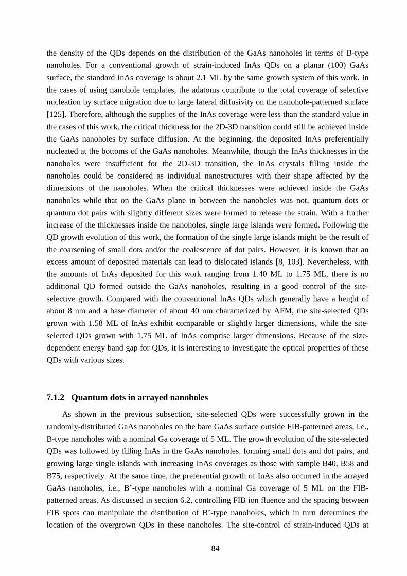
84
the density of the QDs depends on the distribution of the GaAs nanoholes in terms of B-type
nanoholes. For a conventional growth of strain-induced InAs QDs on a planar (100) GaAs
surface, the standard InAs coverage is about 2.1 ML by the same growth system of this work. In
the cases of using nanohole templates, the adatoms contribute to the total coverage of selective
nucleation by surface migration due to large lateral diffusivity on the nanohole-patterned surface
[125]. Therefore, although the supplies of the InAs coverage were less than the standard value in
the cases of this work, the critical thickness for the 2D-3D transition could still be achieved inside
the GaAs nanoholes by surface diffusion. At the beginning, the deposited InAs preferentially
nucleated at the bottoms of the GaAs nanoholes. Meanwhile, though the InAs thicknesses in the
nanoholes were insufficient for the 2D-3D transition, the InAs crystals filling inside the
nanoholes could be considered as individual nanostructures with their shape affected by the
dimensions of the nanoholes. When the critical thicknesses were achieved inside the GaAs
nanoholes while that on the GaAs plane in between the nanoholes was not, quantum dots or
quantum dot pairs with slightly different sizes were formed to release the strain. With a further
increase of the thicknesses inside the nanoholes, single large islands were formed. Following the
QD growth evolution of this work, the formation of the single large islands might be the result of
the coarsening of small dots and/or the coalescence of dot pairs. However, it is known that an
excess amount of deposited materials can lead to dislocated islands [8, 103]. Nevertheless, with
the amounts of InAs deposited for this work ranging from 1.40 ML to 1.75 ML, there is no
additional QD formed outside the GaAs nanoholes, resulting in a good control of the site-
selective growth. Compared with the conventional InAs QDs which generally have a height of
about 8 nm and a base diameter of about 40 nm characterized by AFM, the site-selected QDs
grown with 1.58 ML of InAs exhibit comparable or slightly larger dimensions, while the site-
selected QDs grown with 1.75 ML of InAs comprise larger dimensions. Because of the size-
dependent energy band gap for QDs, it is interesting to investigate the optical properties of these
QDs with various sizes.
7.1.2 Quantum dots in arrayed nanoholes
As shown in the previous subsection, site-selected QDs were successfully grown in the
randomly-distributed GaAs nanoholes on the bare GaAs surface outside FIB-patterned areas, i.e.,
B-type nanoholes with a nominal Ga coverage of 5 ML. The growth evolution of the site-selected
QDs was followed by filling InAs in the GaAs nanoholes, forming small dots and dot pairs, and
growing large single islands with increasing InAs coverages as those with sample B40, B58 and
B75, respectively. At the same time, the preferential growth of InAs also occurred in the arrayed
GaAs nanoholes, i.e., B’-type nanoholes with a nominal Ga coverage of 5 ML on the FIB-
patterned areas. As discussed in section 6.2, controlling FIB ion fluence and the spacing between
FIB spots can manipulate the distribution of B’-type nanoholes, which in turn determines the
location of the overgrown QDs in these nanoholes. The site-control of strain-induced QDs at

85
intentional positions is therefore realized. Figure 7.4 shows large single islands grown in the
arrayed B’-type nanoholes of sample B75. The arrayed GaAs nanoholes were well-organized
along the FIB spots which were created by In+ ion patterning with different patterning parameters.
Compared with those islands grown in the B-type nanoholes on the bare GaAs surface of sample
B75, these islands have a similar shape but a slightly larger size.
Figure 7.4 SEM images for different FIB-patterned areas on sample B75 with site-selected
InAs QDs grown with an InAs coverage of 1.75 ML in FIB-positioned GaAs nanoholes
formed with a nominal Ga coverage of 5 ML. (a) The area with an In+ ion fluence ΦIn of
1 × 10⁵ ions/spot and a spot spacing lspot of 1 µm, (b) ΦIn = 1 × 10
5 ions/spot and lspot = 2 µm,
(c) ΦIn = 3 × 10⁵ ions/spot and lspot = 1 µm, and (d) ΦIn = 3 × 10
5 ions/spot and lspot = 2 µm.
QD pairs of sample B58 grown in the arrayed B’-type nanoholes with a Ga+ ion fluence of
3×10⁵ ions/spot and spacings of 1 µm and 2 µm are shown in Figure 7.5 (a) and (b), respectively.
Considering the probability of GaAs nanoholes positioned by the FIB spots using corresponding
FIB parameters, In+ ion patterning applied for sample B75 has displayed a better ability than
Ga+ ion patterning operated for this sample. This result is consistent with the observation shown

86
in previous section 6.2. Comparing these arrayed QDs with those QDs grown in the randomly-
distributed B-type nanoholes, the structural configurations are close to each other for the case of
either single dots or dot pairs. Interestingly, it is found that the probability of QD pairs is higher
on the FIB-patterned areas than that on the bare GaAs surface of this sample. The probability
ratio by QD pairs to single QDs is about 1:6 with the B-type nanoholes on the bare GaAs surface,
while it is higher than 8:1 with the B’-type nanoholes. As discussed in section 6.2, the B’-type
nanoholes formed on the optimum FIB-patterned areas have larger lateral dimensions and deeper
depths than B-type nanoholes because of the preferential accumulation of Ga droplets at the FIB
spots. The nanoholes with large lateral dimensions can provide more preferential nucleation sites
for the deposited InAs. On the other hand, the great depths suggest large surface chemical
potential gradients which can enhance the accumulation of the deposited InAs in the nanoholes
[125]. Due to sufficient material amounts and enough space inside the B’-type nanoholes, the
formation of dot pairs was preferred over that of single dots with the InAs coverage of 1.58 ML.
However, as discussed in the last subsection with a higher InAs coverage of 1.75 ML, the InAs
coverage was already beyond the amount to generate small QDs or QD pairs. Therefore, only
large single islands (no island pairs) were formed in either the B-type nanoholes or the B’-type
nanoholes of sample B75.
Figure 7.5 (c) and (d) show the topography of QD pairs grown inside the B’-type nanoholes
on two different FIB-patterned areas of sample B58 with the Ga+ ion fluences of 1 × 10
5 ions/spot
and 3 × 10⁵ ions/spot, respectively. From these two FIB-patterned areas, the sizes of the QD pairs
are in the same range. The plot shows an example profile of the QD pairs measured along the
[ ] and [ ] directions from image (c). From the profile of the QD pair, two dots have
different heights of 4.6 nm and 4.0 nm, respectively. The dot base diameters are shown with
73 nm and 48 nm for the higher dot, and 68 nm and 57 nm for the smaller dot along [ ] and
[ ], respectively. The lateral diameters of these QD pairs are found to be comparable to or
slightly larger than those in the B-type nanoholes due to more material accumulation in these
larger B’-type nanoholes. The size of the QDs depends on the real InAs thickness deposited in the
GaAs nanoholes. Nevertheless, the original depth of the GaAs nanoholes underneath the QDs
should be taken into account for the real heights of the QDs. However, due to the self-limiting
growth in the mismatched system for coherent 3D islands, the size distribution is narrow and the
shape is uniform [22]. Therefore, coherent quantum dots with corresponding lateral dimensions
might be considered with similar configurations of the dot heights as well.
To conclude, site-selected QDs could be spatially controlled on the FIB-patterned areas with
various sizes and no additional QDs formed between the nanoholes under these conditions.
Compared to the randomly-distributed cases, a higher probability of QD pairs and larger QDs can
be generated due to more material accumulation and preferential sites at deep and large B’-type
nanoholes. Finally, the site-selected InAs QDs are not only represented in a low density but also
in a spatially designable manner. In other words, these QDs can be positioned arbitrarily with the
help of FIB writing combined with droplet epitaxy, which can be adapted for the applications

87
with specific demands in site control. With the optimized FIB pattern developed in this work,
these square arrays of QDs with a pitch of about 2 μm are suitable for the studies of single QD
spectroscopy.
Figure 7.5 SEM and AFM images for the
site-selected QD pairs grown in the FIB-
positioned GaAs nanoholes on different FIB-
patterned areas of sample B58. (a) The FIB-
patterned area with a Ga+ ion fluence ΦGa of
3 × 10⁵ ions/spot and a spot spacing lspot of
1 µm, (b), (c) ΦGa = 3 × 10⁵ ions/spot and
lspot = 2 µm, and (d) ΦGa = 1 × 10⁶ ions/spot
and lspot = 2 µm. The profiles correspond to
the QD pair shown in image (c) along [ ]
and [ ] directions.

88
7.2 Optical Properties of Quantum Dots in Randomly-distributed
Nanoholes
It was shown in the previous section that the site-selective growth of the InAs QDs successfully
exploited the GaAs nanohole templates. The growth evolution of the QDs was demonstrated by
varying the InAs coverage as well. These QDs grown with different InAs coverages have shown
different dimensions and structures, which can highly influence their optical properties. This
section focuses on the optical properties of the QDs grown in randomly-distributed nanoholes.
The optical properties were investigated by photoluminescence (PL) spectroscopy and the SNOM
technique for the studies of ensembles and single QDs, respectively. In the first subsection, the
ensemble optical properties of the QDs are discussed and also compared with the conventional
strain-induced QDs grown on a planar GaAs surface. In the second subsection, the optical
properties of single QDs are addressed.
7.2.1 Quantum dot ensembles
For studying the ensemble optical properties of InAs QDs grown in GaAs nanoholes, five
QD samples, C40, C46, C58, C65 and C75, were fabricated with different amounts of InAs
coverage ranging from 1.40 ML to 1.75 ML using self-patterned GaAs nanoholes as templates
which were generated with a nominal Ga coverage of 5 ML by droplet epitaxy. For a complete
quantum confinement, these InAs QDs were covered with GaAs capping layers. This subsection
provides an investigation on the QDs grown in the randomly-distributed GaAs nanoholes, i.e., the
B-type nanoholes, which were formed without the influence of FIB pre-patterning.
The PL measurements were performed using a diode laser emitting with a wavelength of
635 nm, i.e., 1.95 eV which is well above the band gap of GaAs, and an excitation power of
5 mW. The details about the PL process for a QD system and the setup can be found in
section 5.4. Using a GaAs nanohole template, the density of the quantum dots depends on that of
the GaAs nanoholes which is about 7.0 × 107 cm
-2 for B-type nanoholes. With a spot size of the
laser of the order of 10-5
cm-2
on the sample surface, the PL spectra were thus generated from an
ensemble of few thousands of quantum dots. Due to the size fluctuations of these QDs, an
inhomogeneous broadening would be expected in the spectra. Usually, the inhomogeneous
broadening is represented by a Gaussian distribution because the sizes of self-assembled QDs are
typically in a Gaussian distribution. For the ensembles of strain-induced InAs QDs, the
experimentally observed FWHM values were typically found between 30 meV and 60 meV
[172].
Figure 7.6 shows five PL spectra (1) to (5) for the five samples with InAs coverages of
1.40 ML, 1.46 ML, 1.58 ML, 1.65 ML and 1.75 ML, respectively. These PL spectra measured at
77 K consist of several PL peaks or bands corresponding to the electron-hole transitions in the
conduction and valence bands of different semiconductor structures. The peaks with the energy
around 1.45 eV (850 nm) correspond to the transitions in wetting layers (WL) which are the 2D
InAs layers on the GaAs surface between the GaAs nanoholes. In the case with the lowest

89
InAs coverage of 1.40 ML, the peak center at 1.366 eV (908 nm) is attributed to the crystalline
nanostructures formed by filling InAs inside the GaAs nanoholes. The FWHM of this peak is
50 meV. With a higher InAs coverage of 1.46 ML, a broad PL band with two small shoulders at
the low energy side can be observed in the PL spectrum. Meanwhile, the PL spectrum maximum
shifts to a lower energy of 1.346 eV (918 nm). According to SK growth, these two emerging low-
energy shoulders indicate the growth of new structures inside the GaAs nanoholes, i.e., the strain-
induced QDs. As the InAs coverage increase further to 1.58 ML and 1.65 ML, the PL bands
broaden significantly together with multiple low- or high- energy shoulders, and move gradually
toward lower energies. The maxima of these two PL bands are at 1.265 eV (980 nm) and 1.247
eV (994 nm), respectively. With an InAs coverage of 1.75 ML, the PL spectrum shifts further to a
lower energy with four overlapping peaks with their maxima at 1.136 eV (1092 nm), 1.172 eV
(1058 nm), 1.204 eV (1030 nm) and 1.238 eV (1002 nm).
Figure 7.6 The ensemble PL
spectra of sample C40, C46,
C58, C65 and C75 with various
amounts of InAs coverage from
1.40 ML to 1.75 ML by PL
spectroscopy at 77 K with an
excitation power of 5 mW. WL
represents the recombination
from the wetting layer.

90
In order to uncover the origin of the PL broadening and the shoulders in the PL bands
following the morphology evolution of InAs QDs in GaAs nanoholes, the excitation power-
dependence measurements were employed to resolve the PL bands of sample C46, C58 and C65
as shown in Figure 7.7, Figure 7.8 and Figure 7.9, respectively. In Figure 7.7 for sample C46
with the InAs coverage of 1.46 ML, there are two peaks observed at 1.256 eV (987 nm) and
1.346 eV (921 nm) with the lowest excitation power as shown in the insert. Among them, the
source for the higher-energy peak might be the same with that observed for sample C40, which is
the transition attributed to the InAs crystalline structures filled inside GaAs nanoholes with an
insufficient InAs thickness for 2D-3D structural transition. The FWHM of this peak from
sample C46, which is about 53 meV, is comparable with the value originated from the peak of
sample C40. However, no discrete excited state originated from this kind of structures is observed
by increasing the excitation power densities. Such behavior is more like a 2D quantum well
structure with step-like densities of states, than like a QD. As described in subsection 7.1.1, these
filled InAs nanostructures which were separated by nanoholes in a layer were suggested to
have their lateral dimensions much larger than the heights. Therefore, they can be considered
as quantum disks (QDk) which have a quasi-2D quantum nature and optical properties
corresponding to those of quantum wells [173]. Therefore, this peak can be assigned to the
transition of the quantum disks with the energy labeled as . On the other hand, the lower-
energy peak at 1.256 eV (E0) is assigned to the ground-state (s-shell) transition of the QDs with
its FWHM of 40 meV which indicates a good size uniformity of the QDs. With the excitation
power increasing, the PL peak with E1 = 1.285 eV (965 nm) appeared representing the first-
excited-state (p-shell) transition of the QDs which has an energy separation of about 29 meV
from the ground-state peak. These two groups of peaks coexisting in the PL spectra of C46 reveal
that the critical InAs coverage for the 2D-3D structural transition is about 1.46 ML for this work.
With a higher InAs coverage of 1.58 ML, the PL spectrum of sample C58 consists of three
overlapping peaks which were resolved by the excitation power-dependency PL spectra as shown
in Figure 7.8. With the lowest excitation power density, the ground-state peak of QDs is resolved
with the energy E0 of 1.221 eV (1016 nm). It has a FWHM about 57 meV, which is broader than
the ground-state peak of the QDs in the previous sample C46. As described in the preceding
subsection 7.1.1, with an InAs coverage of 1.58 ML, there could be two types of QDs in the
GaAs nanoholes as observed on sample B58, which are single QDs and QD pairs with different
dimensions. Therefore, these various QD dimensions can lead to a broadening of size distribution,
and in turn to a widening of the FWHM. As the excitation power increased, the higher excited
states in the QDs were filled one by one, resulting in the presence of first-excited-state and
second-excited-state (d-shell) peaks with the energies E1 of 1.258 eV (986 nm) and E2 of
1.296 eV (957 nm), respectively. Interestingly, the signals from the 2D-like quantum disks are no
longer visible. It implies that the InAs coverage deposited inside the GaAs nanoholes is above the
critical thickness, therefore 3D QDs becomes dominating.

91
Figure 7.9 shows the excitation power-dependency PL spectra for sample C65 with the
InAs coverage of 1.65 ML. With this coverage, the PL signals are mainly attributed to the
recombination from QDs. By varying the excitation power, the peaks from the ground states, the
first, second and third excited states (f shells) of QDs were resolved with energies E0 of 1.161 eV
(1068 nm), E1 of 1.207 eV (1027 nm), E2 of 1.247 eV (994 nm) and E3 of 1.281 eV (968 nm),
respectively. The peak of the ground states was resolved as shown in the insert with the FWHM
of 34 meV for the lowest power density. Compared with sample C58, this sample shows a
smaller value for the FWHM of the ground-state peak. This reduction of the width together with
the increase of InAs coverage implies that the QDs became larger while the size uniformity
became better. Furthermore, this small value of FWHM indicates a high degree of the size
uniformity of QD ensembles, which is desired in optoelectronic applications.
Figure 7.7 Power-dependent PL spectra measured at 77 K for sample C46 with an InAs
coverage of 1.46 ML. I0 denotes the maximum intensity with an excitation power of 5 mW.
E0 and E1 represent the energies corresponding to the ground-state (s-shell) and the first-
excited-state (p-shell) recombination of QDs. represents the energy corresponding to the
recombination of QDks. WL represents the recombination from the wetting layer. The
insert is the PL spectra with the lowest intensity and its Gaussian fitting curve.
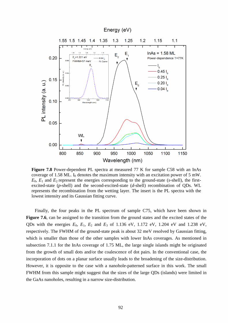
92
Figure 7.8 Power-dependent PL spectra at measured 77 K for sample C58 with an InAs
coverage of 1.58 ML. I0 denotes the maximum intensity with an excitation power of 5 mW.
E0, E1 and E2 represent the energies corresponding to the ground-state (s-shell), the first-
excited-state (p-shell) and the second-excited-state (d-shell) recombination of QDs. WL
represents the recombination from the wetting layer. The insert is the PL spectra with the
lowest intensity and its Gaussian fitting curve.
Finally, the four peaks in the PL spectrum of sample C75, which have been shown in
Figure 7.6, can be assigned to the transition from the ground states and the excited states of the
QDs with the energies E0, E1, E2 and E3 of 1.136 eV, 1.172 eV, 1.204 eV and 1.238 eV,
respectively. The FWHM of the ground-state peak is about 32 meV resolved by Gaussian fitting,
which is smaller than those of the other samples with lower InAs coverages. As mentioned in
subsection 7.1.1 for the InAs coverage of 1.75 ML, the large single islands might be originated
from the growth of small dots and/or the coalescence of dot pairs. In the conventional case, the
incorporation of dots on a planar surface usually leads to the broadening of the size-distribution.
However, it is opposite to the case with a nanohole-patterned surface in this work. The small
FWHM from this sample might suggest that the sizes of the large QDs (islands) were limited in
the GaAs nanoholes, resulting in a narrow size-distribution.

93
Figure 7.9 Power-dependent PL spectra at 77 K for sample C65 with an InAs coverage of
1.65 ML. I0 denotes the intensity with an excitation power of 5 mW. E0, E1, E2 and E3
represent the energies corresponding to the ground-state (s-shell), the first-excited-state (p-
shell), the second-excited-state (d-shell) and the third-excited-state (f-shell) recombination
of QDs. WL represents the recombination from the wetting layer. The insert is the PL
spectra with the lowest intensity and its Gaussian fitting curve.
In order to summarize the evolution of the energy structures of these QDs, the energies for
the transitions of the states are plotted versus InAs coverage as shown in Figure 7.10. As the
InAs coverage increases, the ground-state-transition energies from the QDs represent a red-shift
from 1.256 eV to 1.136 eV. This red-shift is confirmed by the size-dependent energy band gap of
the QDs. However, with the conventional InAs QDs grown on a planar GaAs surface which
comprises lateral diameters of about 40 nm and heights around 8 nm by the same growth system
of this work, the ground-state-transition peak from the ensembles was found at an energy around
1.054 eV (E0) at 77 K as shown in Figure 5.3. Compared to the conventional ones, the quantum
dots grown with nanohole templates are generally larger. Therefore, their ground-state-transition
energies should be lower than 1.054 eV. However, with respect to this energy, varying blue-shifts
from 110 meV to 230 meV are found for the ground-state transitions of these quantum dots with
decreasing sizes. This result is opposite to what would be expected from the quantum
confinement effect. This blue-shift might be attributed to the high Ga concentration in the QDs
which overweights the size dependency in the quantum confinement effect. Since GaAs

94
nanoholes were generated under the condition of arsenic deficiency by droplet epitaxy, a Ga-rich
surface formed on the nanoholes would be expected. Grown on the Ga-rich surface, QDs may
have a high Ga concentration due to the In segregation and the In-Ga intermixing during the
MBE growth of an InAs/GaAs material system [108, 174, 175]. Furthermore, for sample C58, the
energy separation between the s-shell and p-shell transitions of quantum dots is about 37 meV.
This separation is found to be almost the same with that between the next levels, p-shells and
d-shells transitions, which is 38 meV. Such equidistant energies between electron and hole levels
confirm the parabolic potential of lens-shaped QDs in this case. Similar equidistant transition
energies are also found in sample C75 with the separations between s and p, p and d, and d and
f shells of 36 meV, 32 meV and 34 meV, respectively. However, a slightly diminishing energy
separation is found for sample C65, which decreases from 46 meV to 40 meV, and then to
34 meV between the s and p, p and d, and d and f transitions, respectively. In conclusion, the
energy level structures of these QDs are incomparable with those of the conventional ones due to
the fact that the GaAs-nanohole-patterned surface leads to high Ga concentrations and different
morphologies of the QDs. Furthermore, their energy levels are influenced by the size, the
configuration and the composition varied along with the growth evolution. In order to gain more
insight into these QDs and to exclude the effect of the size distribution, an investigation of single
QDs is desired to understand their properties for further applications.
Figure 7.10 The transition energies from the ground states of QDs and QDks (E0 and
), the first, second, and third excited states (E1, E2 and E3) of QDs and wetting
layers (WL), corresponding to the PL spectra of the samples (1) C40, (2) C46, (3)
C58, (4) C65 and (5) C75 with various amounts of InAs coverage. The lines are only
a guide to the eyes.

95
7.2.2 Single quantum dots
The complex energy level structures for the InAs QDs grown in GaAs nanoholes were
proposed in the previous subsection, which was influenced by the interaction of sizes, shapes and
compositions of QDs depending on the growth process. In order to gain further insight, a SNOM
technique allowing micro-scale measurements was used to investigate the optical properties of
these QDs individually, i.e., single QD spectroscopy. For this small-scale measurement, it is
important to determine the location of detected areas precisely. In this work, the desired
areas were defined by an ex-situ photolithography technique as introduced in section 5.1.
On sample C65, one defined area containing QDs grown in the randomly-distributed GaAs
nanoholes on the bare GaAs surface is referred to as the un-patterned area for the following
paragraphs. Figure 7.11 shows the spectrally-integrated PL image measured from this
un-patterned area by a SNOM mapping technique at 10 K. The experimental SNOM settings can
be found in section 5.4. The scanning area is 4.8 × 4.8 μm2 with a pixel size of 80 × 80 nm
2.
Every pixel describes the integrated PL intensity with the energy range from 1.1 eV to 1.3 eV.
For this sample, the QDs were grown with an InAs coverage of 1.65 ML, site-selectively in the
GaAs nanoholes formed with a nominal Ga coverage of 5 ML by droplet epitaxy, i.e., B-type
nanoholes. In the mapping image, the density of these PL bright spots is consistent with that of
the B-type nanoholes on sample B0 without InAs deposition. Since the spatial distribution of the
site-selected QDs depends on that of the GaAs nanoholes, these bright spots can be attributed to
the recombination from the InAs QDs in the GaAs nanoholes individually.
Figure 7.11 The spectrally-integrated PL mapping image for the QDs embedded in
the un-patterned area of sample C65 grown with the InAs coverage of 1.65 ML,
measured at 10 K The integrated energy ranges from 1.1 eV to 1.3 eV. The scanning
area is 4.8 × 4.8 μm2 with a pixel size of 80 ×80 nm
2. The excitation power is
113 W/cm2. (provided by A. Senichev, MPI of Microstructure Physics, Halle).

96
Figure 7.12 The spectrally-integrated PL
mapping image of a bright spot and its cross-
section image, and also the PL spectrum at
10 K. The integrated energy ranges from
1.02 eV to 1.40 eV. The scanning area is
1.0 × 1.0 μm2 with a pixel size of 20 × 20 nm
2.
The arrow is only a guide for showing the
direction of the cross-section image. E00, E10,
E01, and EA are the energies of different
recombinations from the ground states and
excited states of a single QD corresponding to
the bright spot. (provided by A. Senichev, MPI
of Microstructure Physics, Halle).
In order to resolve the quantum structures contributing to the PL bright spots on this sample,
a small scanning area of 1.0 × 1.0 μm2 together with a fine pixel size of 20 × 20 nm
2 was applied
for spectrally-integrated PL mapping, as shown in Figure 7.12. The cross-section image was
extracted from the pixels along the arrow directed through the bright spot. The PL spectrum
shows one strong peak present with E00 = 1.163 eV, two high-energy peaks with E10 = 1.196 eV
and E01 = 1.212 eV, and also one small peak with EA = 1.177 eV. In the cross-section, these peaks
are coexisting at all positions along the bright spot, which indicates no distinguishable fine
structures observed in this condition. Therefore, the constituents of the bright spot can be
suggested as the signals from one uniform quantum structure. The FWHM of the strong peak
with E00 is 8 meV, which is consistent with the transition energies of neutral and charged excitons
in a single quantum dot in the range of 1 meV to 10 meV [53]. Summarizing the observations
above, it can be assumed that the PL bright spot is contributed from a single QD in a nanohole.
Therefore, the peak with E00 can be assigned to the ground-state (s-shell) transition of the QD.
With further experimental results from a power-dependent PL measurement as shown in the
following, the peaks with E10 and E01 can be supposed as the recombination signals from the first
excited states (p shells) of two different parabolic potentials attributed to the anisotropic lateral
confinement of the QD along [ ] and [ ] directions. In addition, the small peaks with EA

97
might originate from the transitions between the ground-state (s-shell) electrons and the second-
excited-state (d-shell) holes in the QD.
Figure 7.13 Power-dependent PL spectra of a single QD with different excitation
power densities from 6 W/cm2 to 379 W/cm
2. E00 is the transition energy of the
ground states. E10, E01, E20, E11 and E02 are the transition energies of the excited
states corresponding to , where x and y are the in-plane
directions, nx and ny are the quantum numbers of the confinements. For example, E10
is the recombination energy of the first excited states from the quantum confinement
along the x direction. EA is considered to be the recombination energy between the
ground-state (s-shell) electrons and second-excited-state (d-shell) holes.
Figure 7.13 shows the PL spectra of a single QD in a B-type nanohole from sample C65
with different excitation power densities. As shown in section 6.1, the B-type nanoholes formed
by droplet epitaxy have an asymmetric wall structure. For the QDs grown on this kind of
nanoholes, a slightly anisotropic QD base is then expected. Therefore, an anisotropic lateral
confinement consisting of two parabolic potentials along the in-plane directions, x and y, can be
applied for this type of asymmetric QDs [36, 176]. The discrete energy levels of QDs can then be
approximated as with the identical quantum numbers nx and ny and
oscillator frequencies x and y [177]. With a low power density, the peak present with the
energy E00 of 1.176 eV and its FWHM of ~ 6 meV is assigned to the ground-state recombination.
A slight red-shift of ~ 1.6 meV is attributed to the occurrence of additional multiexcitonic

98
transitions related to the s shell of the QD [178]. Increasing the power density, more peaks raised
corresponding to the excited states with the energies EA of 1.189 eV, E10 of 1.210 eV, E01 of
1.223 eV, E20 of 1.245 eV, E11 of 1.258 eV, and E02 of 1.276 eV. According to the parabolic
potential, the equidistant quantization energies x and y are found to be about 35 meV and
47 meV, respectively. The oscillation frequency between the electrons and holes can then be
calculated by the relation of h/ e = [2 (E10 − E00) / (EA − E00) – 1]-1
, which is about 0.23 in this
case. From the PL results, the data can be described by the approach of two parabolic potentials
very well.
Figure 7.14 (a) shows 11 individual PL spectra of single QDs that have anisotropic lateral
confinements, in the sequence according to the ground state energies of the QDs. The spectra
correspond to the signals from the bright spots shown in Figure 7.11 with maximum intensities.
The ground-state-transition energies E00 of these single QDs are in the range from 1.140 eV to
1.177 eV. The first-excited-state-transition energies E10 range from 1.184 eV to 1.214 eV, while
the energies E01 from 1.204 eV to 1.223 eV. The FWHM of the ground-state peaks are around
8 meV attributed to the transitions of excitons in a single QD [53]. The energy levels are different
from dot to dot because of the fluctuation of size, morphology and composition. In the plot (b), a
summary for the PL peaks corresponding to each single QD is shown. The energy separations of
E10, E01 and EA with respect to E00 are shown in the plot (c), as a function of the ground-state-
transition energy. With the increasing ground-state energies, the energy separation between E01
and E00, i.e. E01 – E00, shows a stronger decreasing tendency than that with E10 – E00. The energy
separations for EA – E00 only change in a small range of 13 meV to 16 meV. The ground-state-
transition energy E00 can be influenced by the size and the composition of the QD. However,
the single QDs having larger ground-state-transition energies together with smaller energy
separations might be confirmed with higher Ga concentrations. For self-assembled InAs QDs
embedded in a GaAs matrix, the high Ga concentration can be introduced through an intermixing
process in the MBE growth [108, 175, 179]. The fluctuation of the compositions might then be
the result of the diminishing energy separation described in the previous subsection for the PL
data of the QD ensembles.
Concluding the results in this subsection, with a low density benefited from the self-
patterned GaAs nanoholes formed by droplet epitaxy, the InAs QDs can be spatially revolved by
the SNOM technique for single QD investigation. With an InAs coverage of 1.65 ML,
predominant single QDs can be observed which have good optical qualities with a light emission
in the range of the near infra-red. The PL spectra reveal the anisotropic lateral confinements of
these QDs, which are explained by the asymmetric structures of B-type nanoholes where the QDs
were grown site-selectively. The fluctuation of the In-Ga concentration in the quantum dots is
also confirmed by the variation of the discrete energy levels of the QDs.

99
Figure 7.14 (a) The PL data for the
single QDs correspond to the
maximum-intensity signals from the
bright spots, 1 to 11, in Figure 7.11
measured by SNOM. E00 is the
transition energy of the ground states
(s shell). E10 and E01 are the transition
energies of the first excited states
(p shell) with the confinements along
the in-plane directions, x and y,
respectively. EA is considered to be the
transition energy between the ground-
state (s-shell) electrons and second-
excited-state (d-shell) holes. The
dotted lines are only a guide to the
eyes. The plot (b) shows the transition
energies of each QD. The plot (c)
shows the energy separation between
the excited states and the ground states,
as a function of E00. The black dotted
lines is calculated assuming the ratio
h/ e of 0.23. The blue and green
dashed lines are only a guide to the
eyes.
(b) (c)
(a)

100
7.3 Optical properties of Quantum Dots in Arrayed Nanoholes
In the previous sections, the site-selected InAs quantum dots in the randomly-distributed GaAs
nanoholes have been reported with good optical properties on the bare GaAs surface. In this work,
in order to design the distribution of quantum dots with an intentional pattern for novel quantum
devices, site-selected InAs QDs were also generated in the arrayed GaAs nanoholes positioned on
the FIB-patterned areas. However, it is known that FIB pre-patterning may influence the
properties of the sample due to FIB-induced defects. In order to investigate the influence of FIB
pre-patterning and its induced damage on the optical properties of the QDs, several FIB-patterned
areas with different FIB parameters were investigated by PL spectroscopy and the SNOM
technique for QD ensemble and single QD optical measurements, respectively. In the first part,
the experimental results from the ensembles of QDs on the arrayed GaAs nanohole templates are
discussed. In the second part, an insight to the single QDs in the GaAs nanoholes embedded in a
FIB-patterned area is given with the measurement data.
7.3.1 Quantum dot ensembles
The ensembles of site-selected QDs grown in the arrayed GaAs nanoholes of sample C65 are
studied in this subsection for their optical properties measured by PL spectroscopy. These QDs
were grown with an InAs coverage of 1.65 ML. The GaAs nanoholes were formed site-
selectively on the FIB-patterned area with a nominal Ga coverage of 5 ML by droplet epitaxy, i.e.,
B’-type nanoholes. These FIB-patterned areas consisting of square arrays of FIB spots were
created by In+ ion patterning with various ion fluences of 1×10
5 ions/spot, 3×10
5 ions/spot and
1×10⁶ ions/spot together with different spot spacings of 0.5 µm, 1 µm and 2 µm, respectively. As
mentioned in section 5.1, an ex-situ photolithography technique was applied for defining the
position of the investigated regions and quantifying the amounts of QD ensembles participating
in the measurement within an area of 40 × μm2. An area composed of site-selected QDs grown
in the B-type nanoholes without FIB pre-patterning was defined as the un-patterned area of
sample C65. The single QD optical properties from this un-patterned area have been shown in the
previous subsection 7.2.2. In this section, the ensemble PL spectrum from this un-patterned area
is used for a comparison. The PL measurements were carried out at 77 K by a diode laser
emitting at 635 nm with an excitation power of 5 mW. The details about the PL process and the
setup are addressed in section 5.4. According to the observation in section 7.1, using B-type and
B’-type nanoholes as templates for the site-selective growth of QD, the arrangement of the QDs
was found highly dependent on the distribution of these nanoholes. The intrinsic density of the
randomly-distributed B-type nanoholes and the nominal density ρFIB of the arrayed B’-type
nanoholes are both of the order of 107 cm
-2. Therefore, the generation of the PL spectra was
obtained from an ensemble of hundreds of quantum dots in the investigated areas of 40 × μm2.
Therefore, the inhomogeneous broadening in the PL spectra should be considered due to size
fluctuations.
In Figure 7.15, the PL spectra are attributed to the recombinations from the s, p and d shells
of the QDs. The peak for the ground-state (s-shell) transition of the QD ensembles embedded in

101
the un-patterned area (ΦIn = 0 ions/spot) is found with an energy of 1.151 eV (1077 nm) and a
FWHM of about 38 meV obtained by Gaussian fitting. Comparing this un-patterned area with the
FIB-patterned areas generated with a spot spacing of 2 µm together with different ion fluences,
there is no significant difference from the ground-state energies of the QD ensembles, as shown
in the plot (a). On the other hand, for the FIB-patterned areas with a smaller spot spacing of 1 µm,
the ground-state energies are slightly blue-shifted with respect to those for the un-patterned area,
as shown in the plot (b). With an even closer spot spacing of 0.5 µm as shown in the plot (c), the
ground-state energies are blue-shifted in the range of 10 meV for the FIB-patterned areas with
respect to those for the un-patterned area. However, with corresponding spacings, the impact of
ion fluences on the energy level structures of the QDs is found insignificant with these values
from 1 × 10⁵ ions/spot to 1 × 10
6 ions/spot.
Figure 7.15 PL spectra of the site-selected
InAs QDs grown with an InAs coverage of
1.65 ML in the arrayed GaAs nanoholes
formed with a nominal Ga coverage of 5 ML
on the FIB-patterned areas with various In+ ion
fluences of 1 × 10⁵ ions/spot, 3 × 10
5 ions/spot
and 1 × 10⁶ ions/spot together with different
spot spacings of (a) 2 µm, (b) 1 µm, and (c)
0.5 µm. The spectrum for the QDs in the
un-patterned area (ΦIn = 0) is shown in each
graph for comparison.

102
As mentioned in subsection 7.1.2, contrary to the B-type nanoholes on the bare GaAs surface,
the B’-type nanoholes in the optimum FIB-patterned area are larger and deeper which can lead to
a stronger preferential deposition of overgrown InAs, resulting in larger QDs or QD pairs in the
nanoholes. With larger QDs, a red-shift should thus be expected in the PL spectrum compared to
that in the un-patterned area. However, under the condition applied in this work with an arsenic
deficiency for droplet epitaxy, GaAs nanoholes would be expected to have a Ga-rich surface. As
discussed in section 6.2, due to the difference of the surface energies on a FIB-modified surface,
Ga adatoms were locally accumulated on the FIB spots resulting in the formation of Ga droplets
which are larger than those on the un-patterned area. With low arsenic pressure together with
high substrate temperature, the GaAs crystalline substrate would be melted by the liquid droplets
into GaAs molecules by thermal etching, until all the droplet materials were crystallized. With
larger Ga droplets formed on the FIB spots, deeper nanoholes containing a larger Ga-rich region
would then be produced on the FIB-patterned areas. With subsequent InAs deposition, In-Ga
intermixing can take place during the growth, resulting in a high Ga concentration in the QDs
[174, 175]. Therefore, for the QDs on the FIB-patterned areas composed of large GaAs nanoholes
with a Ga-rich surface, the absence of the red-shift might be due to the neutralization by the
increases of the QD size and the Ga concentration.
On the other hand, with the decreasing spot spacings, the blue-shifts may be due to the size
variation of the QDs on different FIB-patterned areas. As discussed in section 6.2, with the ion
fluences ranging from 1 × 10⁵ ions/spot to 1 × 10
6 ions/spot, the nominal density of the nanohole
increased with the decreasing spot spacing. Especially, using a spot spacing of 0.5 µm with the
optimized ion fluence of 3 × 10⁵ ions/spot, the nominal density could be created above the
intrinsic density of the GaAs nanoholes on the bare GaAs surface. With the same amount of the
deposited materials, i.e., a nominal Ga coverage of 5 ML, smaller Ga droplets would be formed
along with higher densities due to Ostwald ripening, which would be transformed into smaller
and shallower GaAs nanoholes by droplet epitaxy. With a shallower depth, the chemical potential
gradients at the nanohole are therefore smaller, which leads to less pronounced preferential
growth for the subsequent InAs deposition. Therefore, with the same supplied InAs coverage of
1.65 ML, less accumulation of the InAs in the smaller nanohole would result in smaller QDs
which in turn result in a blue shift of a PL spectrum. Besides, using the same spot spacing with
the ion fluences of this range, the deviation of the nominal densities of the B’-type nanoholes on
sample B0 is relatively small. A small size fluctuation of the QDs would thus be expected
between these FIB-patterned areas. As a result, the PL spectra of these site-selected QDs display
a dependency weakly on the FIB ion fluence, but relatively significant on the spacing between
FIB spots.
Since the density of the site-selected QD depends on that of the GaAs nanoholes, the density
of the QDs is higher with a smaller FIB spot spacing. However, when the spot spacing of the
FIB-patterned area gets closer, the PL intensities for the QD ensembles generally become weaker.
This decline could possibly resulted from the degradation in the crystal quality of the GaAs
surface due to the damages induced by the energetic ion beam through sputtering or implantation

103
which can present in the form of vacancies or interstitials in the substrate [171]. With a smaller
spot spacing, a higher amount of ion irradiation on the FIB-patterned areas was created since the
sizes of the patterned areas were fixed to be the same. Therefore, the crystal quality of the GaAs
matrix deteriorates because of a great amount of FIB-induced defects. During the PL process,
these defects could be the scattering centers for the charge carriers. The crystalline alteration
owed to FIB patterning reduced the efficiency of electron-hole recombinations, which may
explain the observed decrease in the PL intensity. Especially with dense distributed FIB spots on
the GaAs surface created by a spacing of 0.5 µm, where the ion irradiation was integrated
between the spots, the intensity may drop further when the ion fluence increases.
Concluding these ensemble PL measurements for the FIB-patterned areas, it was revealed
that the site-selected QDs in the arrayed GaAs nanoholes with FIB pre-patterning might represent
different sizes and Ga concentrations compared to those in the un-patterned area, because the
nanohole templates were formed with variations of hole sizes and densities on different FIB-
patterned areas. Therefore, the optical properties of QDs can be tuned with the help of FIB pre-
patterning and droplet epitaxy. However, the optical properties are found not only influenced by
the QD size and density, but also the crystal quality of the sample affected by FIB-induced
defects. Therefore, the controlling and damaging properties of FIB should be carefully taken into
account in order to ensure the efficiency of devices for electrical or optical applications. With a
sufficient distance between the FIB spots, the PL spectra are found less dependent on the ion
fluence in these cases.
7.3.2 Single quantum dots
As discussed in the previous subsection, the ensemble optical properties of InAs QDs in the
arrayed GaAs nanoholes were varied with different FIB parameters. In order to obtain a close
view of these QDs influenced by FIB pre-patterning, the SNOM technique was employed for the
single QD optical characterization. As mentioned in section 6.2, the optimum FIB patterning
parameters for the site control are found to be an ion fluence of 3 × 10⁵ ions/spot with a spot
spacing of 2 µm by In+ ion patterning to achieve a high probability of GaAs nanoholes positioned
on the FIB spots. The FIB-patterned area of sample C65 created with this optimum condition was
chosen for studying single QDs in the positioned GaAs nanoholes. The QDs were grown site-
selectively in the GaAs nanoholes with an InAs coverage of 1.65 ML by SK growth, while the
GaAs nanoholes were formed site-selectively on the FIB pre-patterned area with a nominal Ga
coverage of 5 ML by droplet epitaxy, i.e., B’-type nanoholes. The spectrally-integrated PL
mapping image with a scanning area of 4.8 × 4.8 μm2 and a pixel size of 80 × 80 nm
2 is shown in
Figure 7.16, measured at 10 K. The integration of the PL intensity was made with the energy
range from 1.02 eV to 1.40 eV. The experimental settings of SNOM can be found in section 5.4.
Two bright spots are present in this scanning area. The distance between these two bright spots is
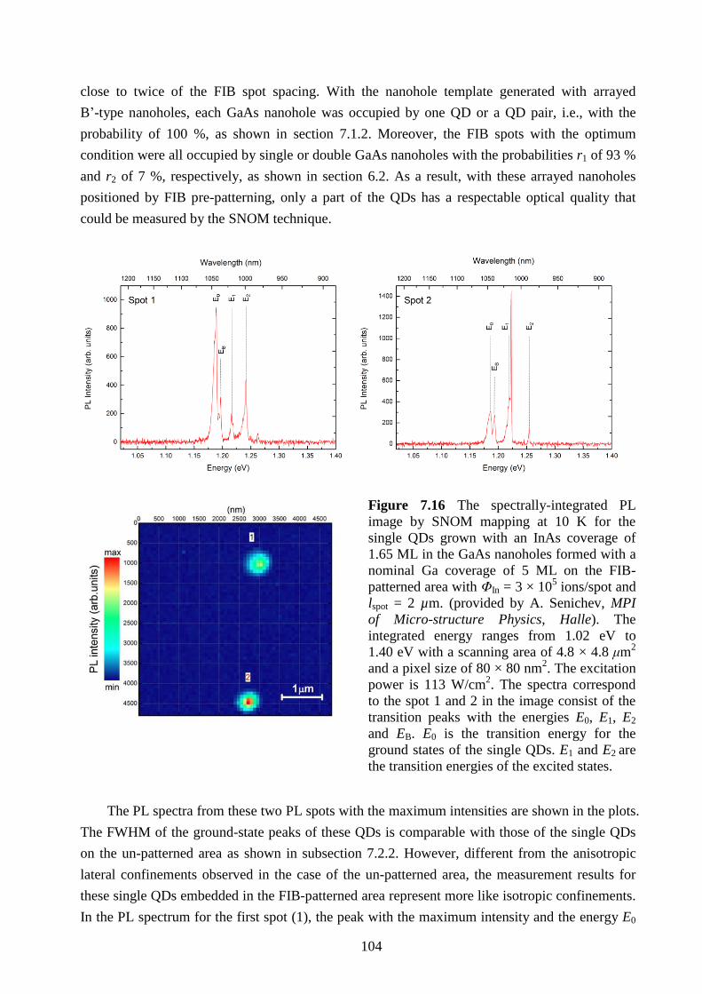
104
close to twice of the FIB spot spacing. With the nanohole template generated with arrayed
B’-type nanoholes, each GaAs nanohole was occupied by one QD or a QD pair, i.e., with the
probability of 100 %, as shown in section 7.1.2. Moreover, the FIB spots with the optimum
condition were all occupied by single or double GaAs nanoholes with the probabilities r1 of 93 %
and r2 of 7 %, respectively, as shown in section 6.2. As a result, with these arrayed nanoholes
positioned by FIB pre-patterning, only a part of the QDs has a respectable optical quality that
could be measured by the SNOM technique.
Figure 7.16 The spectrally-integrated PL
image by SNOM mapping at 10 K for the
single QDs grown with an InAs coverage of
1.65 ML in the GaAs nanoholes formed with a
nominal Ga coverage of 5 ML on the FIB-
patterned area with ΦIn = 3 × 10⁵ ions/spot and
lspot = 2 µm. (provided by A. Senichev, MPI
of Micro-structure Physics, Halle). The
integrated energy ranges from 1.02 eV to
1.40 eV with a scanning area of 4.8 × 4.8 μm2
and a pixel size of 80 × 80 nm2. The excitation
power is 113 W/cm2. The spectra correspond
to the spot 1 and 2 in the image consist of the
transition peaks with the energies E0, E1, E2
and EB. E0 is the transition energy for the
ground states of the single QDs. E1 and E2 are
the transition energies of the excited states.
The PL spectra from these two PL spots with the maximum intensities are shown in the plots.
The FWHM of the ground-state peaks of these QDs is comparable with those of the single QDs
on the un-patterned area as shown in subsection 7.2.2. However, different from the anisotropic
lateral confinements observed in the case of the un-patterned area, the measurement results for
these single QDs embedded in the FIB-patterned area represent more like isotropic confinements.
In the PL spectrum for the first spot (1), the peak with the maximum intensity and the energy E0

105
of 1.189 eV is assigned to the ground-state transition with a FWHM of ~ 6 meV. The energies for
the first- and second-excited-state transitions are E1 = 1.216 eV and E2 = 1.241 eV, respectively.
The equidistant energy separation of 27 meV is consistent with the approach from a parabolic
potential. In the spectrum of the second spot (2), the energy of the peak for ground-state
transitions is E0 = 1.185 eV, and the FWHM amounts to 8 meV. The equidistant energy
separation between the first- and second-excited-state transition peaks is 34 meV, by the energies
E1 = 1.219 eV and E2 = 1.254 eV. However, the peaks with EB from both spots having an energy
separation of 8 meV with respect to their ground-state peaks, EB - E0, are different from the peaks
considered to be the recombination between ground-state electrons and second-excited-state holes
with EA observed in the previous subsection 7.2.2. In addition, the pronounced peak present with
an energy of 1.223 eV for the second spot (2) has a narrow FWHM less than 2 meV which is
much less than the other peaks. These two peaks might correspond to the emission from different
neutral and charged excitons in the same single quantum dot [53] or to the emission raised from a
different dot since the probability of QD pairs can become higher with B’-type nanoholes and the
formation of double GaAs nanoholes is possible in this FIB-patterned area.
Concluding the results in this subsection, the distribution, configuration and optical quality
of site-selected QDs can be changed by using a combination of droplet epitaxy and FIB pre-
patterning to produce various nanohole templates. However, in order to heal the sample crystal
quality which is reduced by the FIB-induced defects, a proper annealing process should be
considered for a future work. Nevertheless, this approach represents a potential way to modify the
distribution of strain-induced QDs, owed to the flexibility of droplet epitaxy and the variable
abilities of FIB writing.


107
Chapter 8 Summary
In order to overcome the limits of strain-induced InAs QDs with respect to their sizes and
densities, a site-selective growth has been demonstrated with an MBE system in this work by
using GaAs nanoholes as templates fabricated by droplet epitaxy with a random distribution or an
organized arrangement, where an in-situ FIB pre-patterning has been employed for the latter.
The GaAs nanoholes were formed on a GaAs epilayer, i.e., homoepitaxy, using the droplet
epitaxy as a self-assembly method, by crystallizing Ga metal droplets under the conditions of low
As pressure and a high substrate temperature. In general, these nanoholes have been represented
with a thermally etched valley surrounded by an asymmetric wall structure due to different
atomic diffusion rates depending on the crystal directions of the substrate surface. On the bare
GaAs surface without FIB pre-patterning, the GaAs nanoholes are randomly distributed with a
low density of the order of 107 cm
-2 which is desired for the studies of single nanostructure
spectroscopy. On the other hand, the GaAs nanoholes on the FIB-patterned area were site-
selectively formed, resulting in an organized order according to the pattern design and the ion
fluence. The optimum patterning parameters have been obtained with an ion fluence of
3 × 10⁵ ions/spot together with a spot spacing of 2 μm by a focused In
+ ion beam with an energy
of 30 keV. FIB pre-patterning with these parameters allows GaAs nanoholes to be well-
positioned in the square arrays of FIB spots with a formation probability of nearly 100 %, where
single nanoholes are dominant. The formation of double, triple or multiple nanoholes can be
achieved by increasing the ion fluence, while the nucleation occurs at the edge of the FIB spots
because of the unintentional exposure from the tail of the ion beam. Moreover, decreasing the
distance of the spot spacing, the nominal density of the GaAs nanoholes on the FIB-patterned
area can be increased to even above the intrinsic density of the nanoholes on the bare GaAs
surface. Compared with the nanoholes on the bare GaAs surface (A-type or B-type nanoholes),
the GaAs nanoholes formed on the optimum FIB-patterned areas (A’-type or B’-type nanoholes)
are generally deeper and wider. This is due to a sufficient thermal etching and the crystallization
with larger Ga droplets resulting from the preferential nucleation of Ga adatoms induced by the
surface energy difference on the FIB-modified surface.
The site control of InAs QDs was realized using B-type and B’-type nanoholes as templates
together with a subsequent MBE growth following the SK mode. Therefore, these QDs are
featured with a low density or an arranged distribution consistent with that of the nanoholes.

108
However, the size and the configuration of the QDs were altered with different amounts of
deposited InAs in the GaAs nanoholes. For various amounts of InAs coverage ranging from
1.40 ML to 1.75 ML, the growth evolution of these QDs could be investigated. First, the
deposited InAs preferentially filled the GaAs nanoholes. Then, single QDs or QD pairs were
formed due to the 2D-3D transition. Finally, large single islands were generated in the nanoholes
by the growth of single dots and/or the coalescence of dot pairs. Meanwhile, the preferential
nucleation of InAs was enhanced in the deep B’-type nanoholes due to large chemical potential
gradients. Therefore, the QDs grown on the optimum FIB-patterned areas have larger dimensions
compared to those on the bare GaAs surface with corresponding amounts of InAs coverage. In
addition, the formation probability for QD pairs is higher on the FIB-patterned area with respect
to that on the bare GaAs surface because the wide B’-type nanoholes contains more preferential
nucleation sites for the deposited InAs. The formation of the QDs was well controlled inside the
nanoholes within this coverage range, so that the site-selective growth of strain-induced QDs was
successfully implemented with an arbitrary manipulation in terms of the sizes and the locations.
A good optical quality of these site-selected InAs QDs has been confirmed from the optical
characterization by photoluminescence (PL) spectroscopy, despite the interruption between the
MBE growths for FIB patterning in the approach of this work. At a low InAs coverage, the quasi-
2D quantum structures, i.e., the quantum disks, present in the PL spectra were attributed to the
filled InAs nanostructures in the GaAs nanoholes with a thickness below the critical value for the
2D-3D transition. With higher amounts of InAs coverage, the PL signals for the QD ensembles
emerged corresponding to the recombinations from the ground states and the excited states. The
red shift of the PL spectra was due to the increase of QD sizes with increasing InAs coverage,
while the narrowed FWHM of the ground-state peaks proposed the improvement of the size
homogeneity. Moreover, the emission energies have revealed a high Ga concentration in these
In(Ga)As QDs which was caused by an intermixing process during the growth with a Ga-rich
surface at the GaAs nanoholes formed under an arsenic deficiency by droplet epitaxy. Calculated
from the ground-state and excited-state energies, the equidistant energy separations are consistent
with the eigenstates of a 2D harmonic oscillator potential which describes the confinement of
lens-shaped QDs [72].
With FIB pre-patterning by In+ ion fluences from 1 × 10
5 ions/spot to 1 × 10
6 ions/spot and
a spot spacing of 2 μm, the ensemble optical properties of the InAs QDs in the positioned GaAs
nanoholes are comparable with those in the randomly-distributed GaAs nanoholes without FIB
pre-patterning. In general, the QDs grown on the FIB-patterned areas with these FIB patterning
conditions have a larger size than those on the bare GaAs surface. Therefore, the consistent
ground-state energies suggested an even higher Ga concentration of these QDs due to the
intermixing with a larger Ga-rich region induced by the deep B’-type nanoholes on the FIB-
patterned areas. However, a slight blue shift was present in the PL spectra as the spot spacing
became closer because the size of the QDs depends on the dimensions of B’-type nanoholes
which were varied with the patterning parameters. Meanwhile, the PL intensity was reduced with

109
the decreasing spot spacing due to the degradation of the crystal quality caused by the integration
of the FIB-induced defects, especially with the smallest distance of 0.5 μm in this work.
Aided by the low density of the GaAs nanoholes, the spectrum of a single QD could be
realized by the SNOM technique for these strain-induced InAs QDs. The optical characteristics of
the single QDs grown on the B-type nanoholes with predominant asymmetric walls have been
explained by the anisotropic lateral confinements. The energy levels of the single QDs can be
well described by the approach with two parabolic potentials along the in-plane directions with
different equidistant energy separations. However, the structures of the QD energy levels were
found different from dot to dot depending on the interactions of size and composition. On the
other hand, an isotropic lateral confinement was shown for the single QDs grown on the B’-type
nanoholes with pronounced valleys formed by sufficient thermal etching. In addition, because the
crystal quality can be degraded by the FIB-induced damage, a compensation of FIB patterning or
an additional annealing process should be considered in order to suppress or heal the defects.
Nevertheless, the results of the optical characterization support the approach combining MBE
growths and FIB writing as a possible pathway to modify the configuration and the distribution of
self-assembled nanoholes leading to the realization of site-selected QDs with various properties.
In conclusion, the site-selective growth for good-quality and low-density In(Ga)As QDs and
QD pairs with intentional arrangements was successfully developed and optimized with self-
assembled/self-patterned GaAs nanoholes, by using the advantages of two completely compatible
MBE growths and the in-situ FIB direct-writing techniques. In terms of confinements, emitting
wavelengths and spatial distributions, this development has broadened the potentials of self-
assembled QDs in fundamental research and also in semiconductor applications, especially for
those based on single QD devices such as single photon sources for quantum cryptography or
qubits for quantum computers [17–20].


111
Bibliography
1. D. Bimberg, M. Grundmann, N.N. Ledentsov, Quantum dot heterostructures (John Wiley
Chichester 1999).
2. A. Zrenner, J. Chem. Phys. 112, 7790 (2000).
3. M.A. Hines, P. Guyot-Sionnest, J. Phys. Chem. 100, 468 (1996).
4. Y. Cao, U. Banin, J. Am. Chem. Soc. 122, 9692 (2000).
5. L.P. Kouwenhoven, D.G. Austing, S. Tarucha, Rep. Prog. Phys. 64, 701 (2001).
6. D. Bimberg, M. Grundmann, N.N. Ledentsov, S.S. Ruvimov, P. Werner, U. Richter, J.
Heydenreich, V.M. Ustinov, P.S. Kop'ev, Z.I. Alferov, Thin Solid Films 267, 32 (1995).
7. K. Watanabe, N. Koguchi, Y. Gotoh, Jpn. J. Appl. Phys. 39, L79-L81 (2000).
8. E. Pehlke, N. Moll, A. Kley, M. Scheffler, Appl. Phys. A-Mater. 65, 525 (1997).
9. D. Leonard, M. Krishnamurthy, S. Fafard, J.L. Merz, P.M. Petroff, J. Vac. Sci. Technol. B
12, 1063 (1994).
10. D. Leonard, M. Krishnamurthy, C.M. Reaves, S.P. Denbaars, P.M. Petroff, Appl. Phys. Lett.
63, 3203 (1993).
11. K. Kamath, P. Bhattacharya, T. Sosnowski, T. Norris, J. Phillips, Electron. Lett. 32, 1374
(1996).
12. R. Mirin, A. Gossard, J. Bowers, Electron. Lett. 32, 1732 (1996).
13. I. Vurgaftman, J.R. Meyer, L.R. Ram-Mohan, J. Appl. Phys. 89, 5815 (2001).
14. D. Bimberg, N. Kirstaedter, N.N. Ledentsov, Z.I. Alferov, P.S. Kop'ev, V.M. Ustinov, IEEE
J. Sel. Top. Quant. 3, 196 (1997).
15. A. Fiore, J.X. Chen, M. Ilegems, Appl. Phys. Lett. 81, 1756 (2002).
16. P. Bhattacharya, X.H. Su, S. Chakrabarti, G. Ariyawansa, A.G.U. Perera, Appl. Phys. Lett.
86, 191106 (2005).
17. P. Michler, A. Kiraz, C. Becher, W.V. Schoenfeld, P.M. Petroff, L. Zhang, E. Hu, A.
Imamoglu, Science 290, 2282 (2000).
18. C. Santori, M. Pelton, G. Solomon, Y. Dale, Y. Yamamoto, Phys. Rev. Lett. 86, 1502
(2001).
19. D. Loss, D.P. DiVincenzo, Phys. Rev. A 57, 120 (1998).
20. G. Burkard, D. Loss, Phys. Rev. B 59, 2070 (1999).
21. P.W. Shor, SIAM J. Comput. 26, 1484 (1997).
22. H.T. Dobbs, D.D. Vvedensky, A. Zangwill, J. Johansson, N. Carlsson, W. Seifert, Phys.
Rev. Lett. 79, 897 (1997).
23. N. Koguchi, K. Ishige, Jpn. J. Appl. Phys. 32, 2052 (1993).

112
24. Z.M. Wang, K. Holmes, Y.I. Mazur, K.A. Ramsey, G.J. Salamo, Nanoscale Res. Lett. 1, 57
(2006).
25. Z. Gong, Z.C. Niu, S.S. Huang, Z.D. Fang, B.Q. Sun, J.B. Xia, Appl. Phys. Lett. 87, 93116
(2005).
26. K. Tung, H. Gao, N. Xiang, J. Cryst. Growth 371, 117 (2013).
27. J.H. Lee, Z.M. Wang, E.-S. Kim, N.Y. Kim, S.H. Park, G.J. Salamo, Nanoscale Res. Lett. 5,
308 (2010).
28. J.H. Lee, Z.M. Wang, Z.Y. Abu Waar, G.J. Salamo, Cryst. Growth Des. 9, 715 (2009).
29. T. Mano, N. Koguchi, J. Cryst. Growth 278, 108 (2005).
30. T. Mano, K. Mitsuishi, Y. Nakayama, T. Noda, K. Sakoda, Appl. Surf. Sci. 254, 7770
(2008).
31. T. Mano, K. Watanabe, S. Tsukamoto, H. Fujioka, M. Oshima, N. Koguchi, J. Cryst. Growth
209, 504 (2000).
32. A.Z. Li, Z.M. Wang, J. Wu, Y. Xie, K.A. Sablon, G.J. Salamo, Cryst. Growth Des. 9, 2941
(2009).
33. Z.M. Wang, K. Holmes, J.L. Shultz, G.J. Salamo, Phys. Status Solidi (a) 202, R85 (2005).
34. Z.M. Wang, B.L. Liang, K.A. Sablon, G.J. Salamo, Appl. Phys. Lett. 90, 113120 (2007).
35. Z.M. Wang, B.L. Liang, K.A. Sablon, J.H. Lee, Y.I. Mazur, N.W. Strom, G.J. Salamo, Small
3, 235 (2007).
36. C. Heyn, A. Stemmann, R. Eiselt, W. Hansen, J. Appl. Phys. 105, 54316 (2009).
37. S.S. Huang, Z.C. Niu, Z.D. Fang, H. Ni, Z. Gong, J.B. Xia, Appl. Phys. Lett. 89, 31921
(2006).
38. C. Zhao, Y.H. Chen, B. Xu, P. Jin, Z.G. Wang, Appl. Phys. Lett. 91, 33112 (2007).
39. Á. Nemcsics, Acta Polytech. Hung. 8, 5 (2011).
40. P. Boonpeng, S. Kiravittaya, S. Thainoi, S. Panyakeow, S. Ratanathammaphan, J. Cryst.
Growth (2013).
41. J.H. Lee, Z.M. Wang, N.W. Strom, Y.I. Mazur, G.J. Salamo, Appl. Phys. Lett. 89, 202101
(2006).
42. B.L. Liang, Z.M. Wang, J.H. Lee, K.A. Sablon, Y.I. Mazur, G.J. Salamo, Appl. Phys. Lett.
89, 43113 (2006).
43. . onso- onz z, . n, . Fust r, . onz z, . onz z, . Mart n z-Pastor,
Appl. Phys. Lett. 91, 163104 (2007).
44. N.W. Strom, Z.M. Wang, J.H. Lee, Z.Y. Abu Waar, Y.I. Mazur, G.J. Salamo, Nanoscale
Res. Lett. 2, 112 (2007).
45. . onso- onz z, . Mart n- nch z, . onz z, . n, . Fust r, . onz z,
Cryst. Growth Des. 9, 2525 (2009).
46. J.H. Lee, Z.M. Wang, B.L. Liang, K.A. Sablon, N.W. Strom, G.J. Salamo, Semicond. Sci.
Tech. 21, 1547 (2006).
47. M. Mehta, D. Reuter, A. Melnikov, A.D. Wieck, A. Remhof, Appl. Phys. Lett. 91, 123108
(2007).
113
48. Y. Cordier, O. Tottereau, L. Nguyen, M. Ramdani, A. Soltani, M. Boucherit, D. Troadec, F.
Lo, Y.Y. Hu, A. Ludwig, Phys. Status Solidi (c) 8, 1516 (2011).
49. H. Wang, J.L. Gray, J. Vac. Sci. Technol. B 29, 04D106 (2011).
50. M. Kammler, R. Hull, M.C. Reuter, F.M. Ross, Appl. Phys. Lett. 82, 1093 (2003).
51. M. Cahay (ed), Quantum confinement VI. Nanostructured materials and devices :
proceedings of the international symposium (Electrochemical Society, Pennington, N.J
2001).
52. E. Kapon, Proc. IEEE 80, 398 (1992).
53. O. Gywat, H.J. Krenner, J. Berezovsky, Spins in optically active quantum dots. Concepts
and methods (Wiley-VCH, Weinheim 2010).
54. B. Szafran, J. Adamowski, S. Bednarek, Physica E 5, 185 (1999).
55. F. Tinjod, Mécanismes de formation des boîtes quantiques semiconductrices, application
aux nanostructures II-VI et étude de leurs propriétés optiques. PhD thesis (Université Joseph
Fourier-Grenoble I 2003).
56. A.I. Ekimov, A.A. Onushchenko, JETP Lett. 34, 345 (1981).
57. A.L. Efros, Sov. Phys. Semicond.+ 16, 772 (1982).
58. S. Kiravittaya, A. Rastelli, O.G. Schmidt, Rep. Prog. Phys. 72, 46502 (2009).
59. A.L. Efros, M. Rosen, Annu. Rev. Mater. Sci. 30, 475 (2000).
60. J.I. Pankove, Optical processes in semiconductors (Courier Dover Publications 1971).
61. T.J. Bukowski, J.H. Simmons, Crit. Rev. Solid State 27, 119 (2002).
62. I.L. Medintz, H.T. Uyeda, E.R. Goldman, H. Mattoussi, Nat. Mater. 4, 435 (2005).
63. V.L. Colvin, M.C. Schlamp, A.P. Alivisatos, Nature 370, 354 (1994).
64. L. Jacak, P. Hawrylak, A. Wójs, Quantum dots (Springer, Berlin [u.a.] 1998).
65. T. Sako, J. Paldus, G.H. Diercksen, The Energy Level Structure of Low-dimensional Multi-
electron Quantum Dots, in: J.R. Sabin, E. Brandas (eds), Theory of confined quantum
systems (Elsevier, Boston 2009).
66. J.-Y. Marzin, G. Bastard, Solid State Commun. 92, 437 (1994).
67. F. Henneberger, J. Puls, C. Spiegelberg, A. Schulzgen, H. Rossman, V. Jungnickel, A.I.
Ekimov, Semicond. Sci. Tech. 6, A41–A50 (1991).
68. J.M. Moison, F. Houzay, F. Barthe, L. Leprince, E. Andre, O. Vatel, Appl. Phys. Lett. 64,
196 (1994).
69. A. Wójs, P. Hawrylak, S. Fafard, L. Jacak, Phys. Rev. B 54, 5604 (1996).
70. D. Leonard, K. Pond, P.M. Petroff, Phys. Rev. B 50, 11687 (1994).
71. O. Wolst, Electro-optical investigations of zero-dimensional nanostructures. Anisotropic
Stark effect in InAs, GaAs self-assembled quantum dots (Lehrstuhl für
Mikrocharakterisierung, Friedrich-Alexander-Universität, Erlangen 2003).
72. R.C. Ashoori, Nature 379, 413 (1996).
73. M. Rontani, F. Rossi, F. Manghi, E. Molinari, Phys. Rev. B 59, 10165 (1999).
74. J. R. Sabin, E. Brandas (eds), Theory of confined quantum systems (Elsevier, Boston 2009).

114
75. H. Drexler, D. Leonard, W. Hansen, J.P. Kotthaus, P.M. Petroff, Phys. Rev. Lett. 73, 2252
(1994).
76. M. Fricke, A. Lorke, J.P. Kotthaus, G. Medeiros-Ribeiro, P.M. Petroff, Europhys. Lett. 36,
197 (1996).
77. L. Bányai, S.W. Koch, Semiconductor quantum dots (World Scientific, Singapore, River
Edge, NJ 1993).
78. H. Welker, H. Weiss, Group III-Group V Compounds, in: F. Seitz, D. Turnbull (eds), Solid
state physics. Advances in research and applications (Academic press, New York 1956).
79. H.H. Wieder, J. Vac. Sci. Technol. 8, 210 (1971).
80. K. Ploog, Annu. Rev. Mater. Sci. 11, 171 (1981).
81. M.A. Herman, H. Sitter 7, Molecular beam epitaxy. Fundamentals and current status
(Springer, Berlin, New York 1996).
82. E. Kuphal, Appl. Phys. A-Mater. 52, 380 (1991).
83. T.F. Kuech, Mater. Sci. Rep. 2, 1 (1987).
84. D.A. Glocker, S.I. Shah, Handbook of thin film process technology (Institute of Physics
Pub., Bristol, U.K 2002).
85. J.S. Blakemore, J. Appl. Phys. 53, R123-R181 (1982).
86. M. Levinshtein, S. Rumyantsev, M. Shur, Handbook series on Semiconductor Parameters
(vol 1). Si, Ge, C (Diamond), GaAs, GaP, GaSb, InAs, InP, InSb (World Scientific 1996).
87. P.K. Tien, Proc. Int. Summer School (1982).
88. F. Capasso, Science 235, 172 (1987).
89. K. Oura, V.G. Lifshits, A.A. Saranin, A.V. Zotov, Surface Science. An Introduction
(Advanced Texts in Physics) (Springer 2003).
90. J.A. Venables, G.D.T. Spiller, M. Hanbucken, Rep. Prog. Phys. 47, 399 (1984).
91. S.A. Chambers, Surf. Sci. Rep. 39, 105 (2000).
92. A.Y. Cho, J. Appl. Phys. 41, 2780 (1970).
93. A.Y. Cho, J.R. Arthur, Prog. Solid State Ch. 10, Part 3, 157 (1975).
94. A.Y. Cho, Thin Solid Films 100, 291 (1983).
95. C. Webb, S.-L. Weng, J.N. Eckstein, N. Missert, K. Char, D.G. Schlom, E.S. Hellman, M.R.
Beasley, A. Kapitulnik, J.S. Harris, Appl. Phys. Lett. 51, 1191 (1987).
96. E.H. Parker, The technology and physics of molecular beam epitaxy (Plenum Press 1985).
97. M.A. Herman, H. Sitter, Molecular beam epitaxy. Fundamentals and current status
(Springer-Verlag, Berlin, New York 1989).
98. R.F.C. Farrow, Molecular beam epitaxy. applications to key materials (William Andrew
Publishing 1995).
99. Riber, Riber MBE 32 operator's guide.
100. D. Reuter, A.D. Wieck, A. Fischer, Rev. Sci. Instrum. 70, 3435 (1999).
101. W. Braun, Applied RHEED. Reflection high-energy electron diffraction during crystal
growth (Springer, Berlin [u.a.] 1999).
102. M. Ohring, Materials science of thin films (Academic press 2001).

115
103. D. Vanderbilt, L.K. Wickham, MRS Proc. 202, 555 (1990).
104. R.M. Roescu, Wavefunctions and carrier-carrier interactions in InAs quantum dots studied
by capacitance-voltage spectroscopy. PhD thesis (Ruhr-Universität Bochum 2008).
105. N.P. Kobayashi, T.R. Ramachandran, P. Chen, A. Madhukar, Appl. Phys. Lett. 68, 3299
(1996).
106. A.-L. Barabási, Appl. Phys. Lett. 70, 2565 (1997).
107. V.A. Shchukin, N.N. Ledentsov, D. Bimberg, Physica E 9, 140 (2001).
108. G. Medeiros-Ribeiro, K. Schmidt, T. Ngo, J.L. Feng, A. Lorke, J. Kotthaus, P.M. Petroff,
Appl. Phys. Lett. 71, 2014 (1997).
109. C. Heyn, Phys. Rev. B 64, 165306 (2001).
110. L.G. Wang, P. Kratzer, N. Moll, M. Scheffler, Phys. Rev. B 62, 1897 (2000).
111. P. Michler, Single semiconductor quantum dots (Springer 2009).
112. I. Daruka, A.-L. Barabási, Phys. Rev. Lett. 79, 3708 (1997).
113. J.H. Lee, Z.M. Wang, N.Y. Kim, G.J. Salamo, Nanotechnology 20, 285602 (2009).
114. Á. Nemcsics, Óbuda University e‐Bulletin 2, 193 (2011).
115. X. Li, G.W. Yang, J. Phys. Chem. C 112, 7693 (2008).
116. X. Li, J. Cryst. Growth 377, 59 (2013).
117. R.M. Stevenson, R.M. Thompson, A.J. Shields, I. Farrer, B.E. Kardynal, D.A. Ritchie, M.
Pepper, Phys. Rev. B 66, 81302 (2002).
118. A. Imamoglu, D.D. Awschalom, G. Burkard, D.P. DiVincenzo, D. Loss, M. Sherwin, A.
Small, Phys. Rev. Lett. 83, 4204 (1999).
119. M. Kitamura, M. Nishioka, J. Oshinowo, Y. Arakawa, Appl. Phys. Lett. 66, 3663 (1995).
120. D.S. Mui, D. Leonard, La Coldren, P.M. Petroff, Appl. Phys. Lett. 66, 1620 (1995).
121. S. Jeppesen, M.S. Miller, D. Hessman, B. Kowalski, I. Maximov, L. Samuelson, Appl. Phys.
Lett. 68, 2228 (1996).
122. R. Tsui, R. Zhang, K. Shiralagi, H. Goronkin, Appl. Phys. Lett. 71, 3254 (1997).
123. A. Konkar, A. Madhukar, P. Chen, Appl. Phys. Lett. 72, 220 (1998).
124. H. Lee, J.A. Johnson, M.Y. He, J.S. Speck, P.M. Petroff, Appl. Phys. Lett. 78, 105 (2001).
125. B.D. Gerardot, G. Subramanian, S. Minvielle, H. Lee, J.A. Johnson, W.V. Schoenfeld, D.
Pine, J.S. Speck, P.M. Petroff, J. Cryst. Growth 236, 647 (2002).
126. P. Atkinson, M.B. Ward, S.P. Bremner, D. Anderson, T. Farrow, G.A. Jones, A.J. Shields,
D.A. Ritchie, Physica E 32, 21 (2006).
127. T. Ishikawa, T. Nishimura, S. Kohmoto, K. Asakawa, Appl. Phys. Lett. 76, 167 (2000).
128. S. Kiravittaya, H. Heidemeyer, O.G. Schmidt, Physica E 23, 253 (2004).
129. S. Kiravittaya, A. Rastelli, O.G. Schmidt, Appl. Phys. Lett. 87, 243112 (2005).
130. S. Kiravittaya, A. Rastelli, O.G. Schmidt, Appl. Phys. Lett. 88, 43112 (2006).
131. S. Kohmoto, H. Nakamura, T. Ishikawa, S. Nishikawa, T. Nishimura, K. Asakawa, Mater.
Sci. Eng. B-Adv. 88, 292 (2002).
132. C.K. Hyon, S.C. Choi, S.-H. Song, S.W. Hwang, M.H. Son, D. Ahn, Y.J. Park, E.K. Kim,
Appl. Phys. Lett. 77, 2607 (2000).

116
133. G. Biasiol, K. Leifer, E. Kapon, Phys. Rev. B 61, 7223 (2000).
134. A. Madhukar, K.C. Rajkumar, P. Chen, Appl. Phys. Lett. 62, 1547 (1993).
135. M. Ozdemir, A. Zangwill, J. Vac. Sci. Technol. A 10, 684 (1992).
136. R. Songmuang, S. Kiravittaya, O.G. Schmidt, Appl. Phys. Lett. 82, 2892 (2003).
137. M. Mehta, Positioning of self-assembled InAs quantum dots by focused ion beam
implantation. PhD thesis (Ruhr-Universität Bochum 2007).
138. M.-Y. Li, J. Lee, Z. Wang, Y. Hirono, J. Wu, S. Song, S.-M. Koo, E.-S. Kim, G.J. Salamo,
Phys. Status Solidi (a) 209, 1075 (2012).
139. La Giannuzzi, F.A. Stevie, Micron 30, 197 (1999).
140. S. Reyntjens, R. Puers, J. Micromech. Microeng. 11, 287 (2001).
141. J.H. Daniel, D.F. Moore, J.F. Walker, J.T. Whitney, Microelectron. Eng. 35, 431 (1997).
142. J.H. Daniel, D.F. Moore, J.F. Walker, Smart Mater. Struct. 9, 284 (2000).
143. M.K. Miller, K.F. Russell, K. Thompson, R. Alvis, D.J. Larson, R. Anderson, S.J. Klepeis,
J.M. Cairney, D.W. Saxey, D. Mcgrouther, Microsc. Microanal. 13, 428 (2007).
144. M. Albrecht, C.T. Rettner, A. Moser, B.D. Terris, Microsyst. Technol. 13, 129 (2006).
145. P.D. Prewett, G.L.R. Mair, Focused ion beams from liquid metal ion sources (Research
Studies Press 1991).
146. A.A. Tseng, Small 1, 924 (2005).
147. A.A. Tseng, K. Chen, C.D. Chen, K.J. Ma, IEEE T. Electron. Pa. M. 26, 141 (2003).
148. J. Melngailis, Nucl. Instrum. Meth. B 80, 1271 (1993).
149. K. Sakaguchi, T. Sekine, J. Vac. Sci. Technol. B 16, 2462 (1998).
150. J. Orloff, L. Swanson, M.W. Utlaut, High resolution focused ion beams. FIB and its
applications: The physics of liquid metal ion sources and ion optics and their application to
focused ion beam technology (Springer 2003).
151. P. Mazarov, A. Melnikov, R. Wernhardt, A.D. Wieck, Appl. Surf. Sci. 254, 7401 (2008).
152. D.R. Kingham, L.W. Swanson, Appl. Phys. A 34, 123 (1984).
153. C.-S. Kim, S.-H. Ahn, D.-Y. Jang, Vacuum 86, 1014 (2012).
154. J. Lindhard, M. Scharff, H.E. Schiøtt, Range concepts and heavy ion ranges (Munksgaard
1963).
155. J.F. Ziegler, M.D. Ziegler, J.P. Biersack, Nucl. Instrum. Meth. B 268, 1818 (2010).
156. L. Frey, C. Lehrer, H. Ryssel, Appl. Phys. A-Mater. 76, 1017 (2003).
157. A. Lugstein, B. Basnar, J. Smoliner, E. Bertagnolli, Appl. Phys. A-Mater. 76, 545 (2003).
158. K.D. Cummings, L.R. Harriott, G.C. Chi, Ostermayer, Jr.,F. W., P.D. Blais, Proc. SPIE
0632, 93 (1986).
159. R.L. Kubena, J.W. Ward, Appl. Phys. Lett. 51, 1960 (1987).
160. J. Orloff, Rev. Sci. Instrum. 64, 1105 (1993).
161. T. v r, . g r-Waldau, M. Eckberg, E.T. Heyen, H. Lage, A.D. Wieck, K. Ploog, J.
Appl. Phys. 72, 1858 (1992).
162. E. Abbe, Arch. Mikrosk. Anat. 9, 413 (1873).
163. Rayleigh, Philos. Mag. 42, 167 (1896).

117
164. G. Binnig, C.F. Quate, Phys. Rev. Lett. 56, 930 (1986).
165. T. Pradeep, Nano. The essentials : understanding nanoscience and nanotechnology
(McGraw-Hill, New York, London 2008).
166. G. Kada, F. Kienberger, P. Hinterdorfer, Nano Today 3, 12 (2008).
167. P.J. Dean, Prog. Cryst. Growth Ch. 5, 89 (1982).
168. J. Tulkki, A. Heinämäki, Phys. Rev. B 52, 8239 (1995).
169. A. Rasmussen, V. Deckert, Anal. Bioanal. Chem. 381, 165 (2005).
170. . hm , . icht r, M. ptitz, . i nau, v. ci. Instrum. 68, 3458 (1997).
171. G.B. Assayag, J. Vac. Sci. Technol. B 11, 2420 (1993).
172. M. Grundmann, N.N. Ledentsov, O. Stier, D. Bimberg, V.M. Ustinov, P.S. Kop'ev, Z.I.
Alferov, Appl. Phys. Lett. 68, 979 (1996).
173. B.L. Liang, P.-S. Wong, T. Tran, V.G. Dorogan, Y.I. Mazur, M.E. Ware, G.J. Salamo, C.-K.
Shih, D.L. Huffaker, Nano Res. 6, 235 (2013).
174. Y. Ji, W. Lu, G. Chen, X. Chen, Q. Wang, J. Appl. Phys. 93, 1208 (2003).
175. F. Heinrichsdorff, M. Grundmann, O. Stier, A. Krost, D. Bimberg, J. Cryst. Growth 195, 540
(1998).
176. C. Heyn, A. Stemmann, T. Köppen, C. Strelow, T. Kipp, M. Grave, S. Mendach, W. Hansen,
Appl. Phys. Lett. 94, 183113 (2009).
177. S.-S. Li, K. Chang, J.-B. Xia, Phys. Rev. B 71, 155301 (2005).
178. A. Rastelli, S. Stufler, A. Schliwa, R. Songmuang, C. Manzano, G. Costantini, K. Kern, A.
Zrenner, D. Bimberg, O.G. Schmidt, Phys. Rev. Lett. 92, 166104 (2004).
179. A.D.B. Maia, E.C.F. da Silva, A.A. Quivy, V. Bindilatti, V.M. de Aquino, I.F.L. Dias, J.
Phys. D Appl. Phys. 45, 225104 (2012).


119
Appendix
A.1 Index for Sample Number
The sample numbers used in this thesis are named for the convenience of description and
understanding. Appendix 1 shows the index of these sample numbers corresponding to the
internal sample numbers at AFP. The internal sample numbers are ordered depending on the
Riber MBE growth sheets which contain the parameters of the growth process.
Sample Ga coverage
[ML]
InAs coverage
[ML]
In cycles
(cycles for normal QD)
Internal Sample
Number
A0 3 0 0 #14105
B0 5 0 0 #14236
A75 3 1.75 9 (10.75) #14108
B75 5 1.75 9 (10.75) #14115
B58 5 1.58 9 (12) #14233
B40 5 1.40 8 (12) #14240
C75 5 1.75 9 (10.75) #14116
C65 5 1.65 9 (11.5) #14203
C58 5 1.58 9 (12) #14235
C46 5 1.46 9 (13) #14297
C40 5 1.40 8 (12) #14242
Appendix 1 Index of the internal sample number at AFP

120
A.2 Mask for Photolithography
Appendix 2 shows the mask layout based on a van der Pauw mesa and a contact mask. In
this work, this mask layout was used to define the position and area of the investigated regions on
the samples for optical measurements. The investigated regions were defined corresponding to
the active regions of the mesa. The contact regions were coated with Au in order to conceal the
undesired signals and to make a visible contrast for the mesa structures.
Appendix 2 The mask layout for mesa and metal contact.

121
A.3 Ion fluence for Planes and Lines
Ion fluence, Φion, is one of the most important parameter of FIB direct writing. As mentioned
in subsection 4.3.3, the ion fluence is defined as number of impinging ions Nion per unit area A:
Φ
.
The number of impinging ions is expressed as:
.
I is the ion beam current measured by the Faraday cup. t is the dwell time calculated from the
frequency f. q is the charge number of ion species, e.g., q = 1 for Ga+ or In
+. e is the elementary
charge of 1.6×10⁻¹⁹
C. i is the number of repeating times.
For the patterning of planes, the writing area is a sum of lines with small distances defined
by the step size s and the increment c. The step size3 is 7.7 nm in this work, which depends on the
deflector and the working area of the FIB system. The area of the plane A is given by the number
of discrete points nx and ny between the distance of (c·s) with the relation of A = (nx c s) × (ny c s)
= nx ny c 2
s 2
. The dwell time t is given by the relation of t = nx ny / f, where f is the frequency.
The ion fluence for planes is thus expressed as follows:
Φ Φ
s
For the patterning of lines, the area is given by A = 2 r (nx c s) where r is the radius of the ion
beam, and the dwell time amounts to t = nx / f. The ion fluence for lines is expressed by following
equation:
Φ Φ
s
3 With a magnification of 1×, the working area of the FIB system used in this work is 505 × 505 µm
2 composed
of 216
×216
pixels with an inter-pixel distance of 7.7 nm which is defined as the step size here.


123
Acknowledgements
In the end, I would like to express my sincere gratitude to all the people who helped me with
the accomplishment of this thesis in various ways.
My deepest gratitude goes first and foremost to Prof. Dr. Andreas D. Wieck, my supervisor,
who offered me the opportunity to pursue my PhD degree in his group. I am grateful for his
constant encouragement and unwavering support. He has greatly inspired and motivated me in
research with his wide scientific knowledge and impressive explanations. His optimistic attitude
and positive energy have helped me overcome the depression and frustration during my study
many a time. Similarly, my heartfelt tribute shall be paid to Prof. Dr. Dirk Reuter for his
instructive guidance and wise advices. He helped me develop the strategy of the experiments with
his wealth experience and thorough deliberation. His substantial contribution to the fulfillment of
this work is ineffaceable. Furthermore, I would like to thank Prof. Dr. Ulrich Köhler for being
willing to be the second referee and providing his valuable suggestions. Without their tuitions,
this thesis could not have reached its present form.
I am greatly indebted to Prof. Dr. Achim W. Hassel who provided me the opportunity to be
a part of International Max Plank Research School for SurMat. Prof. Hassel has provided his
suggestions from a chemist’s point of view injecting different possibilities into our corporations.
I would also like to extend my gratitude to SurMat for offering the scholarship, providing
training courses and holding scientific conferences. At this point, Dr. Rebekka Loschen and
Ms. Elke Gattermann are also acknowledged for their thoughtful organization.
My highly gratitude goes to the collaborators at Max-Planck-Institut für Mikrostrukturphysik
in Halle, Mr. Alexander Senichev for putting his effort into the fruitful SNOM results, and
Dr. Peter Werner for his support of this corporation. Moreover, I would like to thank Institut für
Experimentalphysik IV of Ruhr-Universität Bochum for providing the instrument of SEM. I am
also grateful of Institut für Analytische Chemie-Elektroanalytik und Sensorik of Ruhr-Universität
Bochum for providing the access of AFM measurements and their technical supports. My
gratitude goes to the collaborators at the institute of CRHEA-CNRS in France as well for
their generous supports, especially the technical supports from Mr. Olivier Tottereau,
Mr. Yuan-Yang Xia and Ms. Monique Teisseire, and the scientific discussion with
Dr. Fabrice Semond.
My thanks would go to all the colleagues at AFP for providing a nice working atmosphere
and unconditional helps in the labs. First, I would like to thank Dr. Arne Ludwig for sharing his
knowledge and opinions concerning my work. I would also like to thank my former colleagues
Dr. Razvan Roescu, Dr. Kirill Trunov and Dr. Ashish Rai who helped me to start my first
steps in the group. A special gratitude goes to my office mate Dr. Stepan Shvarkov for his

124
delightful company and numerous helps at work and also in life. I also appreciate the supports
from Sascha Valentin, Rüdiger Sott, Patrick Labud and Markus Greff, concerning
experiments and measurements. Great acknowledgement goes to our skillful technicians,
Rolf Wernhardt, Georg Krotenbruck and Torsten Ermlich for constructing and repairing the
instruments and computer systems, Nadine Viteritti for the delicate sample processing with
photolithography, Ronna Neumann and Swetlana Mazarov for producing LMIS, and also to
our reliable secretaries, Carmen Rockensüß and Heike Büscher for the administration work.
I owe my special and sincere gratitude to my friends, Sani Noor, Nadezhda Kukharchyk,
and Shovan Pal, for putting their valuable time and effort into the comments on the draft. Their
proofreading and suggestions have improved the quality of this thesis a lot.
The financial supports from SurMat, Deutsch-Französische Hochschule (DFH/UFA CDFA
05-06), AFP and CRHEA-CNRS are gratefully acknowledged.
Last, my wholehearted appreciation would go to my beloved family for their loving
considerations and great confidence in me all through these years, and also to my dearest friends
who always listen to my problems and stand by my side without doubt.

125
Curriculum Vitae
Yu-Ying Hu, born 5th
May 1983 in New Taipei, Taiwan.
1989-1991 Sinpu Elementary School, New Taipei, Taiwan
1991-1995 Rongfu Elementary School, New Taipei, Taiwan
1995-1998 Jiangcui Junior High School, New Taipei, Taiwan
1998-2001 Zhongshan Girls High School, Taipei, Taiwan
2001-2005 Bachelor of Science
Department of Engineering and System Science (Material Science)
National Tsing Hua University, Hsinchu, Taiwan
Project: The preparation of electrochromic devices
2005-2008 Master of Science
Department of Engineering and System Science (Material Science)
National Tsing Hua University, Hsinchu, Taiwan
Thesis: Phase transition and related properties of nanocrytalline Zr(N,O)
thin films by unbalanced magnetron sputtering
2009-present PhD candidate and assistant researcher
Lehrstuhl für Angewandte Festkörperphysik,
Ruhr-Universität Bochum, Germany
Surface and Interface Engineering in Advanced Materials (2009-2012),
International Max Plank Research Schools, Germany
Thesis: Site control and optical characterization of InAs quantum dots
grown in GaAs nanoholes