Sinusoidal Oscillators: Feedback Analysisrfic.eecs.berkeley.edu/142/pdf/module21.pdf · An...
53
Berkeley Sinusoidal Oscillators: Feedback Analysis Prof. Ali M. Niknejad U.C. Berkeley Copyright c 2015 by Ali M. Niknejad 1 / 53
Transcript of Sinusoidal Oscillators: Feedback Analysisrfic.eecs.berkeley.edu/142/pdf/module21.pdf · An...

Berkeley
Sinusoidal Oscillators: Feedback Analysis
Prof. Ali M. Niknejad
U.C. BerkeleyCopyright c© 2015 by Ali M. Niknejad
1 / 53

Oscillators
An oscillator is an essential component in communicationsystems, providing a carrier frequency for RF transmission, alocal oscillator (LO) for up- and down-conversion, and atiming reference for data sampling and re-sampling.
Before the advent of electronic oscillators, sinusoidal signalswere generated from motors (which limited the highestfrequency due to mechanical resonance), or from arcs and LCtanks, which were of limited utility.
Wikipedia: At least six researchers independently made thevacuum tube feedback oscillator discovery ... In the summer of1912, Edwin Armstrong observed oscillations in audion radioreceiver circuits and went on to use positive feedback in hisinvention of the regenerative receiver. German AlexanderMeissner independently discovered positive feedback andinvented oscillators in March 1913. Irving Langmuir at GeneralElectric observed feedback in 1913. Fritz Lowenstein may havepreceded the others with a crude oscillator in late 1911...
2 / 53

Electronic (Feedback) Oscillators
Active Device
Feedback
High-Q Resonator
t
T =1
fV0
An oscillator is an autonomous circuit that converts DC powerinto a periodic waveform. We will initially restrict ourattention to a class of oscillators that generate a sinusoidalwaveform.The period of oscillation is determined by a high-Q LC tankor a resonator (crystal, cavity, T-line, etc.). An oscillator ischaracterized by its oscillation amplitude (or power),frequency, “stability”, phase noise, and tuning range.
3 / 53

Oscillators (cont)
Disturbance
Generically, a good oscillator is stable in that its frequencyand amplitude of oscillation do not vary appreciably withtemperature, process, power supply, and external disturbances.
The amplitude of oscillation is particularly stable, alwaysreturning to the same value (even after a disturbance).
4 / 53

Timing Jitter
0.5 1.0 1.5 2.0 2.5 3.0
- 1.0
- 0.5
0.5
1.0
Real oscillators don’t have a precise period of oscillation. Theperiod varies due to phase noise or timing jitter. The phase ofthe signal increases ωt + φn increases linearly but has a smallnoise component φn that causes jitter.In the figure above, the noise is exaggerated greatly. Inpractice, this slight deviation will only be observed if millionsof cycles of the oscillator are overlaid (using a digitaloscilloscope for example).
5 / 53

Phase Noise
ω0
Phase Noise
ω0 + δω
L(δω) ∼ 100 dB
LC Tank Alone
Pow
er S
pect
ral D
esns
ity (P
SD)
Due to noise, a realoscillator does not have adelta-function powerspectrum, but rather avery sharp peak at theoscillation frequency.
The amplitude drops veryquickly, though, as onemoves away from thecenter frequency. E.g. acell phone oscillator has aphase noise that is 100dBdown at an offset of only0.01% from the carrier!
6 / 53

An LC Tank “Oscillator”
eαt cos ω0t
Note that an LC tank alone is not a good oscillator. Due toloss, no matter how small, the amplitude of the oscillatordecays.
Even a very high Q oscillator can only sustain oscillations forabout Q cycles. For instance, an LC tank at 1GHz has aQ ∼ 20, can only sustain oscillations for about 20ns.
Even a resonator with high Q ∼ 106, will only sustainoscillations for about 1ms.
7 / 53

Feedback Perspective
vo
−vo
n
gmvin : 1
Many oscillators can be viewed as feedback systems. Theoscillation is sustained by feeding back a fraction of theoutput signal, using an amplifier to gain the signal, and theninjecting the energy back into the tank. The transistor“pushes” the LC tank with just about enough energy tocompensate for the loss.
8 / 53
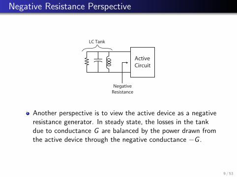
Negative Resistance Perspective
ActiveCircuit
NegativeResistance
LC Tank
Another perspective is to view the active device as a negativeresistance generator. In steady state, the losses in the tankdue to conductance G are balanced by the power drawn fromthe active device through the negative conductance −G .
9 / 53

Reflection Coefficient Perspective
Open or Short |Γ| > 1
Z0, γ = α + jβ
A completely equivalent way to see the negative resistanceargument is to think of the reflection coefficient.Consider launching a wave down a transmission line. Weknow that the wave will have a period equal the round tripdelay td . If we inject a wave into a transmission lineresonator, the signal is attenuated due to the line loss anddecays exponentially.If we can create a load with |Γ| > 1 and the proper phase,then the wave will travel back and forth along the transmissionline without any loss. A negative resistance is thus required.
Γ =Z − Z0
Z + Z0 10 / 53

Feedback Approach
si(s) so(s)+
−a(s)
f(s)
Consider an ideal feedback system with forward gain a(s) andfeedback factor f (s). The closed-loop transfer function isgiven by
H(s) =a(s)
1 + a(s)f (s)
11 / 53

Feedback Example
f
a(s) =a1/30
(1 + sτ)
a(s)
As an example, consider a forward gain transfer function withthree identical real negative poles with magnitude |ωp| = 1/τand a frequency independent feedback factor f
a(s) =a0
(1 + sτ)3
Deriving the closed-loop gain, we have
H(s) =a0
(+sτ)3 + a0f=
K1
(1− s/s1)(1− s/s2)(1− s/s3)12 / 53

Poles of Closed-Loop Gain
Solving for the poles
(1 + sτ)3 = −a0f
1 + sτ = (−a0f )13 = (a0f )
13 (−1)
13
(−1)13 = −1, e j60
◦, e−j60
◦
The poles are therefore
s1, s2, s3 =−1− (a0f )
13
τ,−1 + (a0f )
13 e±j60
◦
τ
13 / 53

Root Locus
jω
σ+60◦
−60◦
−1
τ
a0f = 0
a0f = 8
j√
3/τ
If we plot the poles on thes-plane as a function ofthe DC loop gainT0 = a0f we generate aroot locus
For a0f = 8, the poles areon the jω-axis with value
s1 = −3/τ
s2,3 = ±j√
3/τ
For a0f > 8, the polesmove into the right-halfplane (RHP)
14 / 53

Natural Response
Given a transfer function
H(s) =K
(s − s1)(s − s2)(s − s3)=
a1s − s1
+a2
s − s2+
a3s − s3
The total response of the system can be partitioned into thenatural response and the forced response
s0(t) = f1(a1es1t + a2e
s2t + a3es3t) + f2(si (t))
where f2(si (t)) is the forced response whereas the first termf1() is the natural response of the system, even in the absenceof the input signal. The natural response is determined by theinitial conditions of the system.
15 / 53

Real LHP Poles
e−αt
Stable systems have all poles in the left-half plane (LHP).
Consider the natural response when the pole is on thenegative real axis, such as s1 for our examples.
The response is a decaying exponential that dies away with atime-constant determined by the pole magnitude.
16 / 53
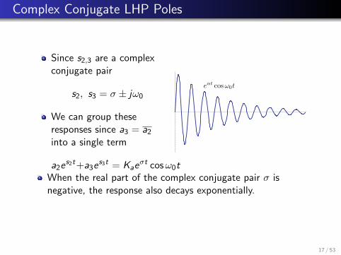
Complex Conjugate LHP Poles
Since s2,3 are a complexconjugate pair
s2, s3 = σ ± jω0
We can group theseresponses since a3 = a2into a single term
a2es2t+a3e
s3t = Kaeσt cosω0t
eαt cos ω0t
When the real part of the complex conjugate pair σ isnegative, the response also decays exponentially.
17 / 53
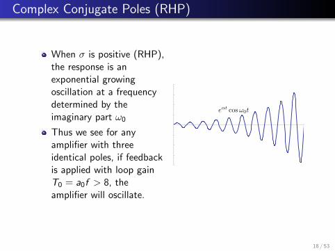
Complex Conjugate Poles (RHP)
When σ is positive (RHP),the response is anexponential growingoscillation at a frequencydetermined by theimaginary part ω0
Thus we see for anyamplifier with threeidentical poles, if feedbackis applied with loop gainT0 = a0f > 8, theamplifier will oscillate.
αte cos ω0t
18 / 53

Frequency Domain Perspective
1
τ
a0f = 8
Closed Loop Transfer Function
In the frequency domainperspective, we see thata feedback amplifier hasa transfer function
H(jω) =a(jω)
1 + a(jω)f
If the loop gain a0f = 8, then we have with purely imaginarypoles at a frequency ωx =
√3/τ where the transfer function
a(jωx)f = −1 blows up. Apparently, the feedback amplifierhas infinite gain at this frequency.
19 / 53
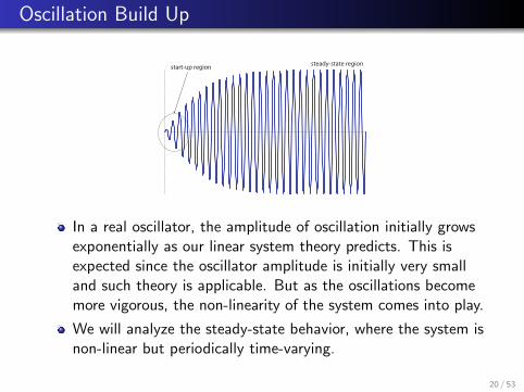
Oscillation Build Up
start-up region steady-state region
In a real oscillator, the amplitude of oscillation initially growsexponentially as our linear system theory predicts. This isexpected since the oscillator amplitude is initially very smalland such theory is applicable. But as the oscillations becomemore vigorous, the non-linearity of the system comes into play.
We will analyze the steady-state behavior, where the system isnon-linear but periodically time-varying.
20 / 53
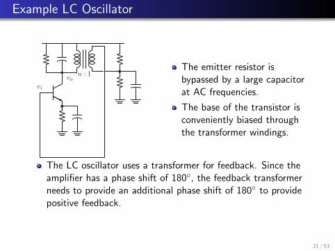
Example LC Oscillator
vo
vi
n : 1The emitter resistor isbypassed by a large capacitorat AC frequencies.
The base of the transistor isconveniently biased throughthe transformer windings.
The LC oscillator uses a transformer for feedback. Since theamplifier has a phase shift of 180◦, the feedback transformerneeds to provide an additional phase shift of 180◦ to providepositive feedback.
21 / 53
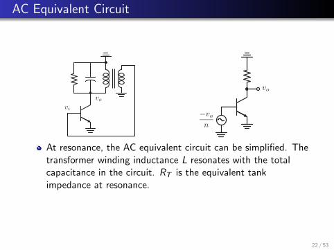
AC Equivalent Circuit
vo
vi
vo
−vo
n
At resonance, the AC equivalent circuit can be simplified. Thetransformer winding inductance L resonates with the totalcapacitance in the circuit. RT is the equivalent tankimpedance at resonance.
22 / 53

Small Signal Equivalent Circuit
roCin gmvin
+vin
−Rin Co
CLRL
L
n : 1
The forward gain is given by a(s) = −gmZT (s), where thetank impedance ZT includes the loading effects from theinput of the transistor
RT = r0||RL||n2Ri
C = Co + CL +Ci
n2
23 / 53

Open-Loop Transfer Function
The tank impedance is therefore
ZT (s) =1
sC + 1RT
+ 1Ls
=Ls
1 + s2LC + sL/RT
The loop gain is given by
af (s) =−gmRT
n
LRT
s
1 + LRT
s + s2LC
The loop gain at resonance is
A` =−gmRT
n
24 / 53

Closed-Loop Transfer Function
The closed-loop transfer function is given by
H(s) =−gmRT
LRT
s
1 + s2LC + s LRT
(1− gmRTn )
Where the denominator can be written as a function of A`
H(s) =−gmRT
LRT
s
1 + s2LC + s LRT
(1− A`)
Note that as n→∞, the feedback loop is broken and wehave a tuned amplifier. The pole locations are determined bythe tank Q.
25 / 53

Oscillator Closed-Loop Gain vs A`
Aℓ < 1
Aℓ = 1
ω0 =
!1
LC
Closed Loop Transfer Function
If A` = 1, then the denominator loss term cancels out and wehave two complex conjugate imaginary axis poles
1 + s2LC = (1 + sj√LC )(1− sj
√LC )
26 / 53

Root Locus for LC Oscillator
For a second order transfer function, notice that themagnitude of the poles is constant, so they lie on a circle inthe s-plane
s1, s2 =−a2b± a
2b
√1− 4b
a2=−a2b± j
a
2b
√4b
a2− 1
|s1,2| =
√a2
4b2+
a2
4b2(
4b
a2+ 1) =
√1
b= ω0
27 / 53

Root Locus (cont)
!!!!!!!!!!
!!!!!!!!!
!
ω0
Aℓ < 1 Aℓ > 1
Aℓ = 1
We see that for A` = 0, the poles are determined by the tankQ and lie in the LHP. As A` is increased, the action of thepositive feedback is to boost the gain of the amplifier and todecrease the bandwidth. Eventually, as A` = 1, the loop gainbecomes infinite in magnitude.
28 / 53

Review: Role of Loop Gain
The behavior of the circuit is determined largely by A`, theloop gain at DC and resonance. When A` = 1, the poles ofthe system are on the jω axis, corresponding to constantamplitude oscillation.
When A` < 1, the circuit oscillates but decays to a quiescentsteady-state.
When A` > 1, the circuit begins oscillating with an amplitudewhich grows exponentially. Eventually, we find that the steadystate amplitude is fixed.
29 / 53

Steady-State Analysis
start-up region steady-state region
To find the steady-state behavior of the circuit, we will makeseveral simplifying assumptions. The most importantassumption is the high tank Q assumption (say Q > 10),which implies the output waveform vo is sinusoidal.
Vω2 ≈1
jωCIω2
Since the feedback network is linear, the input waveformvi = vo/n is also sinusoidal.We may therefore apply the large-signal periodic steady-stateanalysis to the oscillator. For the BJT, we can use themodified Bessel functions.
30 / 53

Steady-State Waveforms
vo
vi
VCC
VBE,Q
IQ
The collector current is not sinusoidal, due to the large signaldrive.
The output voltage,though, is sinusoidal and given by
vo ≈ Iω1ZT (ω1) = GmZT vi
31 / 53
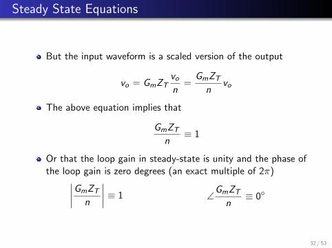
Steady State Equations
But the input waveform is a scaled version of the output
vo = GmZTvon
=GmZT
nvo
The above equation implies that
GmZT
n≡ 1
Or that the loop gain in steady-state is unity and the phase ofthe loop gain is zero degrees (an exact multiple of 2π)
∣∣∣∣GmZT
n
∣∣∣∣ ≡ 1 ∠GmZT
n≡ 0◦
32 / 53

Large Signal Gm
Recall that the small-signal loop gain is given by
|A`| =
∣∣∣∣gmZT
n
∣∣∣∣
Which implies a relation between the small-signal start-uptransconductance and the steady-state large-signaltransconductance ∣∣∣∣
gmGm
∣∣∣∣ = A`
Notice that gm and A` are design parameters under ourcontrol, set by the choice of bias current and tank Q. Thesteady state Gm is therefore also fixed by initial start-upconditions.
33 / 53

Large Signal Gm (BJT)
0.2
0.4
0.6
0.8
1
2 4 181614121086 20
Gm
gm(b)
b
To find the oscillation amplitude we need to find the inputvoltage drive to produce Gm.For a general non-linearity, we need to generate this curveusing numerical integration (Fourier Series).The large signal Gm for an arbitrary non-linearity F (·) is givenby
Gm = Iω1/Vi =1
π
∫ 2π
0F (Vi cos(ωt)) cos(ωt)dt
34 / 53
Large Signal Gm (BJT cont)
For a BJT, we found that under the constraint that the biascurrent is fixed
Iω1 =2I1(b)
I0(b)IQ = Gmvi = Gmb
kT
q
Thus the large-signal Gm is given by
Gm =2I1(b)
bI0(b)
qIQkT
=2I1(b)
bI0(b)gm
Gm
gm=
2I1(b)
bI0(b)
35 / 53

Large Signal Gm (Differential Pair)
0 5 10 15 200.0
0.2
0.4
0.6
0.8
1.0
Gm
gm
b =Vi
kTq
For a differential pair (BJT), we can use numerical integrationto find the ratio of the large signal Gm to the small-signal gm.The nth harmonic (single-ended) output is given by:
Iωn/IEE =
∫ 2π
0
− cos(nt)
π(eb cos(t) + 1
)dt
36 / 53
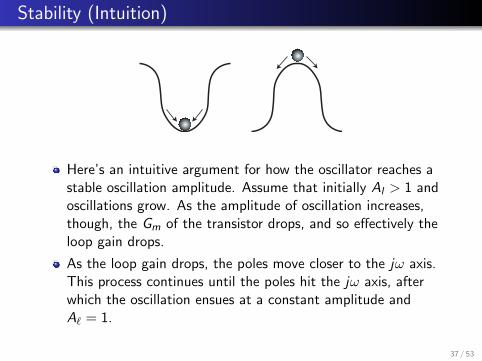
Stability (Intuition)
Here’s an intuitive argument for how the oscillator reaches astable oscillation amplitude. Assume that initially Al > 1 andoscillations grow. As the amplitude of oscillation increases,though, the Gm of the transistor drops, and so effectively theloop gain drops.
As the loop gain drops, the poles move closer to the jω axis.This process continues until the poles hit the jω axis, afterwhich the oscillation ensues at a constant amplitude andA` = 1.
37 / 53
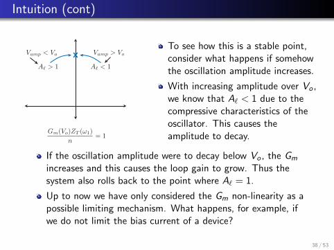
Intuition (cont)
A < 1A > 1
Vamp > VoVamp < Vo
Gm(Vo)ZT (ω1)
n= 1
To see how this is a stable point,consider what happens if somehowthe oscillation amplitude increases.
With increasing amplitude over Vo ,we know that A` < 1 due to thecompressive characteristics of theoscillator. This causes theamplitude to decay.
If the oscillation amplitude were to decay below Vo , the Gm
increases and this causes the loop gain to grow. Thus thesystem also rolls back to the point where A` = 1.
Up to now we have only considered the Gm non-linearity as apossible limiting mechanism. What happens, for example, ifwe do not limit the bias current of a device?
38 / 53
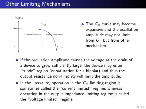
Other Limiting Mechanisms
Ro(Vo)
Vo
Vsat
Current Limited Region Voltage Limited Region
The Gm curve may becomeexpansive and the oscillationamplitude may not limitfrom Gm but from othermechanism.
If the oscillation amplitude causes the voltage at the drain ofa device to grow sufficiently large, the device may enter“triode” region (or saturation for a bipolar) and thus theoutput resistance non-linearity will limit the amplitude.
In the literature, operation in the Gm limiting region issometimes called the “current limited” regime, whereasoperation in the output impedance limiting regime is calledthe “voltage limited” regime.
39 / 53

BJT Oscillator Design
Say we desire an oscillation amplitude of v0 = 100mV at acertain oscillation frequency ω0.
We begin by selecting a loop gain A` > 1 with sufficientmargin. Say A` = 3.
We also tune the LC tank to ω0, being careful to include theloaded effects of the transistor (ro , Co , Cin, Rin)
We can estimate the required first harmonic current from
Iω0 =voR ′T
40 / 53
Design (cont)
This is an estimate because the exact value of RT is notknown until we specify the operating point of the transistor.But a good first order estimate is to neglect the loading anduse R ′TWe can now solve for the bias point from
Iω1 =2I1(b)
I0(b)IQ
b is known since it’s the oscillation amplitude normalized tokT/q and divided by n. The above equation can be solvedgraphically or numerically.
Once IQ is known, we can now calculate R ′′T and iterate untilthe bias current converges to the final value.
41 / 53

Squegging
Squegging is a parasitic oscillation in the bias circuitry of theamplifier.
It can be avoided by properly sizing the emitter bypasscapacitance
CE ≤ nCT
42 / 53
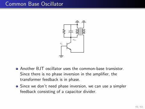
Common Base Oscillator
vo
vi
Another BJT oscillator uses the common-base transistor.Since there is no phase inversion in the amplifier, thetransformer feedback is in phase.
Since we don’t need phase inversion, we can use a simplerfeedback consisting of a capacitor divider.
43 / 53

Colpitts Oscillator
The cap divider works at higher frequencies. Under the cap
divider approximation f ≈ C1
C1 + C ′2=
1
n
n = 1 +C ′2C1
C ′2 includes the loading from the transistor and current source.
44 / 53

Colpitts Bias
Since the bias current is held constant by a current source IQor a large resistor, the analysis is identical to the BJToscillator with transformer feedback. Note the output voltageis divided and applied across vBE just as before.
45 / 53
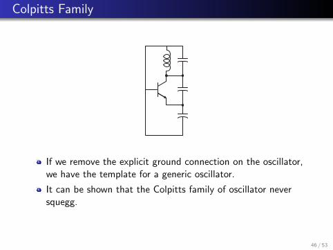
Colpitts Family
If we remove the explicit ground connection on the oscillator,we have the template for a generic oscillator.
It can be shown that the Colpitts family of oscillator neversquegg.
46 / 53

CE and CC Oscillators
If we ground the emitter, we have a new oscillator topology,called the Pierce Oscillator. Note that the amplifier is in CEmode, but we don’t need a transformer!
Likewise, if we ground the collector, we have an emitterfollower oscillator.
A fraction of the tank resonant current flows through C1,2. Infact, we can use C1,2 as the tank capacitance.
47 / 53

Pierce Oscillator
Iω1
If we assume that the current through C1,2 is larger than thecollector current (high Q), then we see that the same currentflows through both capacitors. The voltage at the input and
output is therefore vo = Iω1
1
jωC1
vi = −Iω1
1
jωC2or
vovi
= n =C2
C1
48 / 53

Pierce Bias
A current source or large resistor can bias the Pierce oscillator.
Since the bias current is fixed, the same large signal oscillatoranalysis applies.
49 / 53

Common-Collector Oscillator
Note that the collector can be connected to a resistor withoutchanging the oscillator characteristics. In fact, the transistorprovides a buffered output for “free”.
50 / 53

Clapp Oscillator
CB
C1
C2
RB
The common-collector oscillator shown above uses a largecapacitor CT to block the DC signal at the base. RB is usedto bias the transistor.
If the shunt capacitor CT is eliminated, then the capacitor CB
can be used to resonate with L and the series combination ofC1 and C2. This is a series resonant circuit.
51 / 53

Relaxation Oscillator
Vout
C R
RR
Instead of using an LC tanks as the reference frequency, arelaxation oscillator uses an electronic delay element (RC or Iand R).
Suppose that the output is railed at the positive supply. Thecapacitor C is charged through a resistor until the referencelevel at V+ is crossed (VDD/2), at which point the outputtransitions to the negative rail (V− > V+), and C isdischarged until it reaches the lower reference (−VSS/2).Then the cycle repeats.
52 / 53

Ring Oscillator
In CMOS technology, ring oscillators are ubiquitous. Ifinverters are used, an odd number of stages will oscillate(unstable) and the oscillation period is twice the delay of theline.
Differential versions can be built with an even number ofstages by inverting the phase.
The oscillation frequency can be controlled by varying thedelay of each element using a “current starved” topology.
53 / 53