Sinusoid Signal Generator for On-chip Impedance Spectroscopy
4
Sinusoid Signal Generator for On-chip Impedance Spectroscopy Daniel Rairigh, Student Member, IEEE, Xiaowen Liu, Chao Yang and Andrew J. Mason, Senior Member, IEEE Electrical and Computer Engineering, Michigan State University, East Lansing, Michigan USA Abstract—Compact signal generators are a necessary component for many biomedical and chemical sensor microsystems. This paper presents a signal generator with precise digital frequency control that is 62% smaller the previous designs. The signal generator can produce analog sine waves and digital cosine waves from 4.8 Hz to 39 kHz with a SFDR greater than 99 dB. In a 0.5 μm CMOS process the total signal generator area is 361μm × 1048μm. I. INTRODUCTION Many biomedical and chemical sensors currently under development fall into the impedance-based micro array class of sensors [1, 2], which is defined by three attributes: the sensors present a complex change in resistance and capacitance; the arrays are most useful when operated in high density, and the arrays are small enough to be integrated into a microsystem. To support high density array microsystems, it is crucial that front-end instrumentation circuitry be formed at the chip scale [3], ideally monolithically with sensor interfaces as illustrated in Fig. 1. Such integration requires the instrumentation to be very area efficient in order to rapidly measure the response of all array elements. To address this demand for impedance-based sensors, we have recently introduced a compact impedance-to-digital converter (IDC) [4] that realizes on-chip extraction of real and imaginary impedance components. To fully integrate impedance spectrum instrumentation functions on a single chip, the IDC block requires a companion integrated circuit that generates stimulus and reference signals. This signal generator must also be as small as possible to maximize the number of IDC blocks that can be instantiated on the readout chip. To support a wide range of micro-sensor interfaces and IDC functionality, the signal generator should be capable of producing a sine wave stimulus in the 1Hz to 10kHz range and a digital reference phase shifted by 90° (digital cosine) from the stimulus. Many methods for sinusoid signal generation have been reported in commercial products and research papers. DSP- based solutions generate the sinusoidal signal using digital signal construction [5], where frequency tuning is achieved by varying the memory that updates the clock. To maintain reasonable design requirements on the output filter, the update clock frequency must be high, even for low output sinusoidal frequencies. Thus, a very high signal oversampling ratio is expected, and prohibitively large memory is needed. Quadrature oscillators can also be used to generate quadrature signals [6], but the output frequency is controlled by a tunable component that is difficult to adjust over the required four orders of frequency range. A subthreshold, widely tunable, CMOS transconductance has been reported to provide a frequency range over seven decades [7], but it does not control frequency very accurately. For nonlinear transfer function based signal generators [8], a triangle wave can be generated and transformed to sine wave through a nonlinear transformation using bipolar transistors. However, triangle- to-sine generators always have poor linearity because the quality of the nonlinear transfer function is hard to control. This paper presents a signal generator which is controlled purely by digital signals, allowing excellent frequency accuracy to be easily achieved, unlike the oscillators and non- linear transform generators, and without the large memories of the DSP approach. Compared to our earlier design [9], the signal generator in this paper reduces the area by 62%. II. ARCHITECTURE AND CIRCUIT REALIZATION A. Operation Principles The block diagram for the new signal generator is shown in Fig. 2. The frequency selector is a 14-bit shift register that stores the factor by which the master clock is to be divided. The clock divider is a simple counter with a digital comparator. Master clock cycles are counted until the counter value equals the value stored in the shifter register, at which point a pulse is sent to the token ring and the counter resets. The token ring tracks the current output sample of the sine wave and increments this value with each pulse from the clock divider. The token ring also determines the state of the digital cosine. The resistive DAC (RDAC) is a resistor chain with sinusoidally spaced taps. These taps are selected by the output of the token ring in the proper sequence to generate the next sine wave sample. Finally, the filter removes high frequency quantization replicas from the RDAC signal. Frequency range and coverage are determined by the number of bits in the frequency selector and the over sampling ratio (OSR) of the RDAC. The output frequency is Fig. 1: A complete sensor microsystem consisting of instrumentation circuitry in the IC and sensors fabricated on the surface. Each sensor requires its own IDC, therefore reducing the area required by the signal generator increases the number of sensors that can be integrated. 978-1-4244-3828-0/09/$25.00 ©2009 IEEE 1961
Transcript of Sinusoid Signal Generator for On-chip Impedance Spectroscopy

Sinusoid Signal Generator for On-chip Impedance Spectroscopy
Daniel Rairigh, Student Member, IEEE, Xiaowen Liu, Chao Yang and Andrew J. Mason, Senior Member, IEEE Electrical and Computer Engineering, Michigan State University, East Lansing, Michigan USA
Abstract—Compact signal generators are a necessary component for many biomedical and chemical sensor microsystems. This paper presents a signal generator with precise digital frequency control that is 62% smaller the previous designs. The signal generator can produce analog sine waves and digital cosine waves from 4.8 Hz to 39 kHz with a SFDR greater than 99 dB. In a 0.5 μm CMOS process the total signal generator area is 361μm × 1048μm.
I. INTRODUCTION Many biomedical and chemical sensors currently under
development fall into the impedance-based micro array class of sensors [1, 2], which is defined by three attributes: the sensors present a complex change in resistance and capacitance; the arrays are most useful when operated in high density, and the arrays are small enough to be integrated into a microsystem. To support high density array microsystems, it is crucial that front-end instrumentation circuitry be formed at the chip scale [3], ideally monolithically with sensor interfaces as illustrated in Fig. 1. Such integration requires the instrumentation to be very area efficient in order to rapidly measure the response of all array elements. To address this demand for impedance-based sensors, we have recently introduced a compact impedance-to-digital converter (IDC) [4] that realizes on-chip extraction of real and imaginary impedance components. To fully integrate impedance spectrum instrumentation functions on a single chip, the IDC block requires a companion integrated circuit that generates stimulus and reference signals. This signal generator must also be as small as possible to maximize the number of IDC blocks that can be instantiated on the readout chip. To support a wide range of micro-sensor interfaces and IDC functionality, the signal generator should be capable of producing a sine wave stimulus in the 1Hz to 10kHz range and a digital reference phase shifted by 90° (digital cosine) from the stimulus.
Many methods for sinusoid signal generation have been
reported in commercial products and research papers. DSP-based solutions generate the sinusoidal signal using digital signal construction [5], where frequency tuning is achieved by varying the memory that updates the clock. To maintain reasonable design requirements on the output filter, the update clock frequency must be high, even for low output sinusoidal frequencies. Thus, a very high signal oversampling ratio is expected, and prohibitively large memory is needed. Quadrature oscillators can also be used to generate quadrature signals [6], but the output frequency is controlled by a tunable component that is difficult to adjust over the required four orders of frequency range. A subthreshold, widely tunable, CMOS transconductance has been reported to provide a frequency range over seven decades [7], but it does not control frequency very accurately. For nonlinear transfer function based signal generators [8], a triangle wave can be generated and transformed to sine wave through a nonlinear transformation using bipolar transistors. However, triangle-to-sine generators always have poor linearity because the quality of the nonlinear transfer function is hard to control. This paper presents a signal generator which is controlled purely by digital signals, allowing excellent frequency accuracy to be easily achieved, unlike the oscillators and non-linear transform generators, and without the large memories of the DSP approach. Compared to our earlier design [9], the signal generator in this paper reduces the area by 62%.
II. ARCHITECTURE AND CIRCUIT REALIZATION
A. Operation Principles The block diagram for the new signal generator is shown in
Fig. 2. The frequency selector is a 14-bit shift register that stores the factor by which the master clock is to be divided. The clock divider is a simple counter with a digital comparator. Master clock cycles are counted until the counter value equals the value stored in the shifter register, at which point a pulse is sent to the token ring and the counter resets. The token ring tracks the current output sample of the sine wave and increments this value with each pulse from the clock divider. The token ring also determines the state of the digital cosine. The resistive DAC (RDAC) is a resistor chain with sinusoidally spaced taps. These taps are selected by the output of the token ring in the proper sequence to generate the next sine wave sample. Finally, the filter removes high frequency quantization replicas from the RDAC signal.
Frequency range and coverage are determined by the number of bits in the frequency selector and the over sampling ratio (OSR) of the RDAC. The output frequency is
Fig. 1: A complete sensor microsystem consisting of instrumentation circuitry in the IC and sensors fabricated on the surface. Each sensor requires its own IDC, therefore reducing the area required by the signal generator increases the number of sensors that can be integrated.
978-1-4244-3828-0/09/$25.00 ©2009 IEEE 1961

nMff clk
sig = (1)
where fclk is the rate of the master clock, n is the OSR and M is the value stored in the frequency selector. In our implementation, M can be set to any value from 2 to 16,383 (0x3fff). Thus, with a 5MHz master clock and OSR of 64, the output frequency range is 4.8Hz - 39kHz. In the highest output decade, 19 frequency points can be selected. In the lowest decade over 14,000 frequencies point can be selected. This allows very precise coverage of the lower frequencies and sufficient coverage at higher frequencies for targeted impedance measurement applications. B. Token Ring
The token ring used in [9] consumed the majority of the total signal generator area. The quarter wave token ring used in this design requires 70% fewer D Flip Flops (DFFs) to realize the same function, thus significantly reducing the total area. An example token ring is shown in Fig. 3. This token ring only stores the position within the current quarter of the sine wave, and it uses the slope and sign states to determine which quarter of the sine wave is currently being output. The states of the token ring are illustrated in Fig. 4. Within the S0 to S4 chain, only a single DFF stores a “1” at any given time. The “1” propagates down the chain, and when it reaches the end of the chain, the slope or sign state changes and the direction of propagation reverses. Note that the slope state is equal to the digital cosine of the sinusoid. C. RDAC
An RDAC was used to generate the analog sine wave signal. Fig. 2 shows a simplified example of an RDAC with nine taps. The resistor chain is tapped unevenly according to a sinusoidal waveform. The sine wave is generated by closing one switch at a time at a constant rate. The sign bit of the token ring determines whether the upper or lower half of the chain is currently being used, and the S0 to S4 bits determine which switch in that half is currently closed.
The most important parameter of the RDAC is the number
of taps along the resistor chain, which determines the OSR of the output sinusoid waveform. Although more taps improve linearity, they require more silicon area for switches and control signal routing and more circuitry for switching control. Thus, for a compact design, it is preferable to lower the OSR and employ a low pass filter (LPF) to further suppress the replicas. Based on an analysis of hardware area and complexity of switch control logic, an OSR of 64 was chosen, requiring only 33 taps. With an OSR of 64, the Spurious Free Dynamic Range (SFDR) of the RDAC’s sinusoid output is limited by frequency spurs at 64±1 times the desired signal frequency. To achieve 70dB linearity, the LPF is needed to provide additional suppression of the spurs.
For high DAC linearity, resistor matching is very important, and a resistor chain of 1000 identical unit-value resistors has been implemented. The tapping points are mapped into points between 0 and 1000 to fit a sinusoid. At each tap, a switch is included to generate the sine wave signals. To save silicon area and simplify control logic, these switches were implemented with single NMOS transistors. D. Variable Filter
As described above, the LPF needs to drop off rapidly so
Fig. 3: Quarter wave token ring for a nine tap RDAC. The token ring stores one ¼ of the points in a full period as well as the current sign and slope states.The small numbers at the bottom of each DFF denote the initial state of the DFF after system reset.
Fig. 4: Illustration of quarter wave token ring states. The numbers denote which DFF is storing a 1 at each point in time. The blue and red mark which half of the token ring is being used. The solid line denotes the time durring which the slope is negative.
Fig. 2: Block diagram of signal generator. Frequency is entirely digitally cotrolled to provide high frequency accuracy. The RDAC and filter are designed to provide high linearity.
1962
that the signal frequency (fsig) is fully passed while strongly attenuating the frequency components at 63×fsig. A second order Butterworth filter was chosen for this role because of its flat pass band and rapid attenuation. The Butterworth filter was implemented with a gm-C biquadratic filter, as shown in Fig. 5, where the value of C1 was set to be twice that of C2. To accommodate the four decades of frequency range required in this design, the filter must support four programmable cut off frequencies (fc). These cut offs were achieved by making both the gm and capacitor values programmable as specified in Table I.
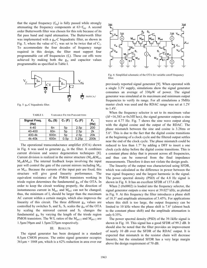
The operational transconductance amplifier (OTA) shown
in Fig. 6 was used to generate gm in the filter. It combines current division and source degeneration techniques [8]. Current division is realized in the mirror structure (Mn1&Mn2, Mn3&Mn4). The internal feedback loops involving the input pair will control the gate of the current mirrors including Mn1 or Mn3. Because the currents of the input pair are fixed, this structure will give good linearity performance. The equivalent resistance of the PMOS transistors working in triode region determines the fundamental gm of the OTA. In order to keep the circuit working properly, the direction of instantaneous current in Mpa1 and Mpa2 can not be changed; thus, the minimum of Is should be larger than the maximum AC current within a certain margin, which also improves the linearity of this circuit. The three different gm values are controlled by switches S1 and S2. S1 scales the gm of the OTA by scaling the mirrored current and S2 changes the fundamental gm by varying the length of the triode region PMOS transistors. The W/L ratios of the Mpa1/2 and Mpb1/2 are 1.5μm/39μm and 1.5μm/225μm respectively.
III. RESULTS The signal generator has been designed in a standard
0.5μm CMOS process. The entire signal generator occupies 361μm × 1048 μm, which is a 62% reduction in area over our
previously reported signal generator [9]. When operated with a single 3.3V supply, simulations show the signal generator consumes an average of 330μW of power. The signal generator was simulated at its maximum and minimum output frequencies to verify its range. For all simulations a 5MHz master clock was used and the RDAC range was set at 1.2V to 1.4V.
When the frequency selector is set to its maximum value (M =16,383 or 0x3fff hex), the signal generator outputs a sine wave at 4.77 Hz. Fig. 7 shows the sine wave output along with the digital cosine and the output of the RDAC. The phase mismatch between the sine and cosine is 3.28ms or 5.6°. This is due to the fact that the digital cosine transitions at the beginning of a clock cycle and the filtered output settles near the end of the clock cycle. The phase mismatch could be reduced to less than 1.7° by adding a DFF to insert a one clock cycle delay before the digital cosine transitions. This is a constant phase delay that is present across all frequencies, and thus can be removed from the final impedance measurements. Therefore it does not violate the design goals.
The linearity of the output was characterized using SFDR, which was calculated as the difference in power between the true signal frequency and the largest harmonic in the signal. The power spectral density (PSD) of the 4.8 Hz signal is shown in Fig. 8. It has an excellent SFDR of 137.6 dB.
When 2 (0x0002) is loaded into the frequency selector, the signal generator outputs a sine wave at 39.027 kHz, as plotted in Fig. 9. At this frequency the filter introduces a phase shift of 18.3° and amplitude attenuation of 3.45%. For applications where this shift is too large, the output frequency can be limited to 10 kHz where the phase shift is 7.6° (almost back to the constant phase shift) and the amplitude attenuation is only 0.35%.
The power spectral density (PSD) of the 39.1kHz signal is shown in Fig. 10. This signal has a good SFDR of 99.2 dB. It should also be noted that the filter provides an improvement of nearly 10 dB over the SFDR of the RDAC output. It is expected that mismatch in the resistor chain will decrease linearity, but the simulated SFDR has a very large margin above the design requirement of 70 dB.
Fig. 5: gm-C biquadratic filter.
TABLE I. VARIABLE FILTER PARAMETERS
Signal Freq. (Hz)
Gm (S) C1 (F) C2 (F) Fc(Hz)
4-40 6n 5p 2.5p 200 40-400 60n 5p 2.5p 2k 400-4k 600n 5p 2.5p 20k 4k-40k 600n 0.5p 0.25p 200k
Fig. 6: Simplified schematic of the OTA for variable cutoff frequency filter.
1963

IV. CONCLUSION Integrated circuit signal generators are a critical component
of impedance based sensor microsystems. This paper presented a compact signal generator that provides precise digital frequency control. The signal generator is designed around a sinusoidally tapped resistor chain, which is clocked from a digital control block. A four decade programmable filter is applied to the resistor chain output to increase linearity of the final signal. The signal generator was shown to have an output frequency range of 4.8Hz - 39kHz and maintain a SFDR of at least 99dB. The total signal generator size in a 0.5 μm CMOS process is only 361μm × 1048μm, permitting it to be implemented on a chip with an array of impedance extraction circuit blocks to provide instrumentation for high density sensor arrays.
ACKNOWLEDGMENT This work has been supported by the National Science
Foundation under Award Number DBI-0649847 and the Defense Advanced Research Project Agency contract number HR0011-08-C-0147.
REFERENCES [1] E. Katz, I. Willner, "Probing Biomolecular Interactions at Conductive and Semiconductive Surfaces by Impedance Spectroscopy: Routes to Impedimetric Immunosensors, DNA-Sensors, and Enzyme Biosensors," Electroanalysis, vol. 15, no. 11, pp. 913-947, Jul .2003. [2] F. Giess, M. G. Friedrich, J. Heberle, R. L. Naumann, W. Knoll, "The Protein-Tethered Lipid Bilayer: A Novel Mimic of the Biological Membrane," Biophys. J, vol. 87, no. 5, pp. 3213-3220, Nov .2004. [3] D. Rairigh, A. Mason, C. Yang, "Analysis of On-Chip Impedance Spectroscopy Methodologies for Sensor Arrays," Sensor Letters, vol. 4, no. 4, pp. 398-402, Dec .2006. [4] C. Yang, S. R. Jadhav, R. M. Worden, A. J. Mason, "Compact Low-Power Impedance to Digital Converter for Sensor Array Microsystems," J. Solid State Cir., (in review). [5] AFG3000 Series Arbitrary/Function Generators, Tektronix, Inc.. http://www.tek.com/products/signal_sources/. [6] I. A. Khan, S. Khwaja, "An integrable gm-C quadrature oscillator," Int. J. of Electronics, vol. 87, no. 11, pp. 1353 - 1357, Nov .2000. [7] T. Serrano-Gotarredona, B. Linares-Barranco, "7-decade tuning range CMOS OTA-C sinusoidal VCO," Electronics Letters, vol. 34, no. 17, pp. 1621-1622, .1998. [8] S. Franco, Design with Operational Amplifier and Analog Integrated Circuits, 3rd, McGraw-Hill, 2002. [9] C. Yang, A. J. Mason, "Fully Integrated 7-Order Frequency Range Quadrature Sinusoid Signal Generator," IEEE Trans. Instrumentation Measurement, (in press).
Fig. 9: Output at 39.1 kHz, the signal generator’s highest output frequency. The filter has removed the discretized steps from the RDAC output. At this high frequency the filter introduces a small amplitude and phase shift as well.
Fig. 8: Power spectral density of the 4.77 Hz output shows a SFDR of 137.6 dB.
Fig. 7: Output at 4.77 Hz, the signal generator’s lowest output frequency. The filter has removed the discretized steps from the the RDAC output and the digital cosine is in phase with the analog output.
Fig. 10: Power spectral density of the 39.1 kHz output shows a SFDR of 99.2 dB.
1964