Single-Phase DVR with Semi-Z-Source Inverter for Power ...
15
Arab J Sci Eng DOI 10.1007/s13369-017-2841-3 TECHNICAL NOTE - ELECTRICAL ENGINEERING Single-Phase DVR with Semi-Z-Source Inverter for Power Distribution Network V. K. Remya 1 · P. Parthiban 1 · V. Ansal 1 · Avinash Nandakumar 1 Received: 26 May 2017 / Accepted: 4 October 2017 © King Fahd University of Petroleum & Minerals 2017 Abstract A novel topology of single-phase dynamic volt- age restorer (DVR) is proposed to compensate the load voltage during voltage sag and voltage swell events. The semi-Z-source converter is utilised in its inverter operat- ing mode for this proposed topology. The reduction in the number of active switches in the inverter and also in the current conduction path without compromising the output voltage range is the merit of the semi-Z-source inverter-based DVR against the commonly used full-bridge inverter-based DVR. The load voltage contains harmonics within the per- missible limits when the compensation is performed by the semi-Z-source inverter-based DVR. The need for the filter circuit is eliminated; hence, the magnitude difference and the phase shift in the inverter output voltage due to the filter circuit are not present in the semi-Z-source inverter- based DVR. The proposed topology is cheap compared to the full-bridge inverter-based DVR topology. The simulations performed in MATLAB/Simulink environment are presented to validate the performance of the proposed topology. A com- parison between the semi-Z-source inverter-based DVR and full-bridge inverter-based DVR is presented in this paper. The novel topology of DVR using semi-Z-source inverter is B V. K. Remya [email protected] P. Parthiban [email protected] V. Ansal [email protected] Avinash Nandakumar [email protected] 1 Department of Electrical and Electronics Engineering, National Institute of Technology, Karnataka, Surathkal, Mangalore, Karnataka 575025, India proved to be a better solution to the full-bridge inverter-based DVR. Keywords Voltage sag · DVR · Semi-Z-source inverter · Modified sinusoidal pulse width modulation (MSPWM) · Feedforward controller · Feedback controller 1 Introduction Industries have attained tremendous growth rate in recent years with the advent of computers and sophisticated equip- ment. Excellent product quality, reduction in manpower and financial profit obtained from this modern method of indus- trialisation have opened the market for sensitive equipment and control systems, automated manufacturing units and computerised process controls. The significant gain in rev- enue received made such systems popular in the industrial arena irrespective of their initial cost. Most of the processes involving this equipment are disturbed and sometimes even damaged by the voltage quality problems. Disturbances in the working environment and economic unbalance are expe- rienced in the industries whenever the utility power deviates from the pre-specified quality. Power quality (PQ) is a matter of great concern to sensitive industrial customers. The PQ issues have a great influence on the profit, end product quality and equipment wellness. Among the various PQ problems, voltage sag is the most severe issue [1]. Through temporary shutdowns, deteriorated products and damaged equipment, sags majorly affect the paper, semiconductor and chemical industries [2, 3]. Voltage sag is the reduction in the rms value of the voltage from 0.9 to 0.1 p·u for a short duration of 0.5 cycles to less than one minute, usually occurring due to faults in the transmission and distribution lines. Voltage sags reported in the litera- 123
Transcript of Single-Phase DVR with Semi-Z-Source Inverter for Power ...

Arab J Sci EngDOI 10.1007/s13369-017-2841-3
TECHNICAL NOTE - ELECTRICAL ENGINEERING
Single-Phase DVR with Semi-Z-Source Inverter for PowerDistribution Network
V. K. Remya1 · P. Parthiban1 · V. Ansal1 · Avinash Nandakumar1
Received: 26 May 2017 / Accepted: 4 October 2017© King Fahd University of Petroleum & Minerals 2017
Abstract A novel topology of single-phase dynamic volt-age restorer (DVR) is proposed to compensate the loadvoltage during voltage sag and voltage swell events. Thesemi-Z-source converter is utilised in its inverter operat-ing mode for this proposed topology. The reduction in thenumber of active switches in the inverter and also in thecurrent conduction path without compromising the outputvoltage range is themerit of the semi-Z-source inverter-basedDVR against the commonly used full-bridge inverter-basedDVR. The load voltage contains harmonics within the per-missible limits when the compensation is performed by thesemi-Z-source inverter-based DVR. The need for the filtercircuit is eliminated; hence, the magnitude difference andthe phase shift in the inverter output voltage due to thefilter circuit are not present in the semi-Z-source inverter-basedDVR. The proposed topology is cheap compared to thefull-bridge inverter-based DVR topology. The simulationsperformed inMATLAB/Simulink environment are presentedto validate the performance of the proposed topology.A com-parison between the semi-Z-source inverter-based DVR andfull-bridge inverter-based DVR is presented in this paper.The novel topology of DVR using semi-Z-source inverter is
B V. K. [email protected]
Avinash [email protected]
1 Department of Electrical and Electronics Engineering,National Institute of Technology, Karnataka, Surathkal,Mangalore, Karnataka 575025, India
proved to be a better solution to the full-bridge inverter-basedDVR.
Keywords Voltage sag · DVR · Semi-Z-source inverter ·Modified sinusoidal pulse width modulation (MSPWM) ·Feedforward controller · Feedback controller
1 Introduction
Industries have attained tremendous growth rate in recentyears with the advent of computers and sophisticated equip-ment. Excellent product quality, reduction in manpower andfinancial profit obtained from this modern method of indus-trialisation have opened the market for sensitive equipmentand control systems, automated manufacturing units andcomputerised process controls. The significant gain in rev-enue received made such systems popular in the industrialarena irrespective of their initial cost. Most of the processesinvolving this equipment are disturbed and sometimes evendamaged by the voltage quality problems. Disturbances inthe working environment and economic unbalance are expe-rienced in the industries whenever the utility power deviatesfrom the pre-specified quality.
Power quality (PQ) is amatter of great concern to sensitiveindustrial customers. The PQ issues have a great influenceon the profit, end product quality and equipment wellness.Among the various PQ problems, voltage sag is the mostsevere issue [1]. Through temporary shutdowns, deterioratedproducts and damaged equipment, sags majorly affect thepaper, semiconductor and chemical industries [2,3]. Voltagesag is the reduction in the rms value of the voltage from 0.9to 0.1p·u for a short duration of 0.5 cycles to less than oneminute, usually occurring due to faults in the transmissionand distribution lines. Voltage sags reported in the litera-
123

Arab J Sci Eng
Fig. 1 Basic block diagram of DVR
ture are mostly having a reduction down to 40–50% of thenominal line voltage and lasting up to < 2s [1]. The faultconditions mostly single-line-to-ground fault (SLGF), start-ing of large motor drives, energisation of the transformersand animal contact are some of the reasons for voltage sagswhich adversely affect the sensitive loads [4,5]. Voltage sagsare characterised by magnitude, duration and phase jump, ifany. The location of the fault from the sensitive load, associ-ated impedances of the transformers, conductors and relatedequipment, voltage class of the feeder, the speed of responseof load protection switchgear are the factors determining themagnitude and duration of the sag experienced by the sensi-tive loads [1,6].
A dynamic voltage restorer (DVR) protects the sensitiveloads from experiencing the PQ problems and diminishes thepotential losses caused by these issues. The DVR is a powerquality device, which restores the load voltage during volt-age quality events (particularly sags and swells) by injectingthe appropriate voltage in series with the supply voltage. TheDVR restores the magnitude and phase of the load voltagecompletely, irrespective of the utility disturbances, therebyallowing control of real and reactive power exchangebetweenthe DVR and the distribution system [1,3,7]. It is the mosteconomical solution for mitigating upstream voltage distur-bances in the distribution system [8].
Conventionally in the DVR system, the inverter outputvoltage (vinv) is injected into the distribution line through aninjection transformer, as shown in Fig. 1. The basic DVRstructure consists of energy storage for real power injec-tion, the inverter for synthesising the required voltage to beinjected into the power line, the filter for removing switchingharmonics from injected voltage and the injection trans-former for voltage boosting and galvanic isolation betweenthe inverter and the line [9]. The voltage requirement of theinverter can be reduced by choosing proper turns ratio ‘n’ ofthe transformer, and it also prevents the input dc source of theinverter frombeing short circuited through the switches in thedifferent inverter legs [10]. A bypass equipment or crowbar
circuit is provided to protect the DVR from the abnormallyhigh downstream load and fault currents [11].
Usually for cost-effectiveness, theDVR installation is per-formed with 50% voltage injection capability. The voltagerating of theDVRdepends on themaximumvoltage injectioncapability and the nominal line voltage of the utility supply.The existing load and the future expansion of the load areconsidered while selecting the current rating of the DVR.Either DVR must be rated to handle the higher currents dur-ing load expansion or the system should be protected usingthe bypass equipment [6].
TheDVR loadvoltage compensation is associatedwith theexchange of active power and reactive power with the utilitygrid. The active power supply to the load demands the need ofa source for this energy. Based on this consideration, DVRis classified into one with stored energy and another withno stored energy. The DVR topologies with stored energyexhibit improved performance for certain types of sags whencompared to its counterpart. The current drawn from theutility grid remains unchanged, and hence, the strain on theutility grid is lower in the case of the energy storage-basedDVR. The two categories in energy storage-based DVR are(a) variable dc-link voltageDVRwhere energy is stored in thedc-link capacitors and (b) constant dc-link voltage DVR. Thebattery, Superconducting Magnetic Energy Storage (SMES)or supercapacitors are some of the direct storage methodsused in the constant dc-link voltage DVR [12].
The DVR topologies with no storage offer cost benefitsdue to the elimination of the energy storage system. In DVRtopologies with no energy storage, a passive shunt converteris used to charge the dc-link capacitor from the grid, andaccording to the location of the shunt converter, the sub-classifications are named as (a) supply-side-connected shuntconverter-based DVR and (b) load-side-connected shuntconverter-based DVR. These topologies draw more currentfrom the grid during sag conditions, and hence, the sen-sitive loads will experience a higher voltage drop. On theother hand, the nonlinear currents drawn by the load-side-connected shunt converter can even disturb the load [12].
A capacitor with voltage control can be used to realise thedc source of the voltage source inverter (VSI) of the DVR. Asthe compensating voltage is injected in quadrature with theline currents, the capacitor-supported DVR neither suppliesnor absorbs active power during the steady-state operation[13,14]. As the restored voltage is not in-phase with the pre-sag/swell voltage, the performance is limited to the certainsag conditions where the phase jump caused by the quadra-ture voltage injection is affordable [13,15].
The way in which the compensation is conducted to main-tain the load voltage constant depends on the type of theload—whether it is magnitude sensitive, phase sensitive orboth. The load reaction to magnitude variation and phasedisturbance during the sag events are studied and analysed.
123

Arab J Sci Eng
Fig. 2 DVR voltagecontrollers. a Feedforwardvoltage controller, b feedbackvoltage controller, c modifiedfeedback voltage controller
The compensation method is selected according to the sever-ity of the disturbance on the load. The conventional voltageinjection schemes are in-phase compensation, pre-sag com-pensation and energy optimised compensation, as elaboratedin the literature [16].
For the appropriate injection of the DVR voltage, voltagecontrollers are used. The most commonly used DVR voltagecontrollers are feedforward, feedback andmodified feedbackvoltage controllers [17,18]. Due to its simplicity and robust-ness, the feedforward controller given in Fig. 2a is widelyused. In this control method, the DVR reference voltage isdetermined by comparing the supply voltage with the loadreference voltage. The response of the feedback control isquick and more accurate as it uses either the load voltage
or DVR voltage in the feedback loop as given in Fig. 2b, c,respectively. The modified feedback control which uses theDVRvoltage in the feedback loop ismore accurate comparedto the feedback control.
The VSI is the most essential element of the DVR.The performance of the DVR system is influenced by theinverter topology. The switching frequency, number of powerswitches in the current path, the number of active and passivedevices, the harmonic content in the inverter output volt-age and the need for the filter are some of the parametersto be considered while selecting the inverter topology [17].Table 1 compares the commonly used inverters in the single-phase and three-phaseDVR system [19–30]. The three-phaseinverter and four-switching leg inverter for three-phase DVR
123

Arab J Sci Eng
Table 1 Comparison of commonly used inverter topologies in the DVR
Sl. no. Inverter Merits Demerits
1 Half-bridge inverter Reduced switch count and low cost Harmonic content present in the voltage ishigh. Filter is required
2 Full-bridge or H-bridge inverter Used in high-voltage distribution system.Independent single-phase connectionavailable
Harmonic content is high. Filter isrequired
3 Three-phase inverter Lower cost and simpler control Filtering scheme is required due toharmonics in the inverter output.Presence of differential and commonmode EMI
4 Four-switching leg inverter No dc-link capacitor balancing problem Presence of differential and commonmode EMI
5 Multilevel inverter Low switching frequency, low devicestress, low THD and low switchinglosses
Increase in number of switching devices.Complex structure after level 5
6 Cascaded multilevel inverter Medium and high-voltage applications,simpler filter design, low harmonics andless losses
Increase in number of switching devices.Complex control and structure
applications and half-bridge and full-bridge inverters usedin both single-phase and three-phase DVR systems requirefilter circuits. The inverter-side filtering scheme in the DVRsystem introduces a magnitude difference due to the passivefilter component voltage drop and the phase shift between theinverter output voltage and the reference voltage waveform.Figure 3 shows the phase shift in the inverter output voltagein a single-phase full-bridge inverter-based DVR when it iscompensating a sag of 40% depth. The phase shift due to thepresence of filter inductance and its equivalent series resis-tance (ESR) prevents the DVR from the exact tracking of thereference voltages generated. The magnitude and phase dif-ference in the fundamental component of voltage before andafter the filter circuit may even jeopardise the DVR control[31]. The lag/lead compensators are introduced in the con-trol strategy to compensate for the phase shift [24]. However,the lag/lead compensator demands an adaptive nature dueto the temperature dependence of the ESR. The alternativeline-side filtering scheme can make use of the leakage reac-tance of the secondary winding of the injection transformeras a filter inductance along with a capacitor. Nevertheless,the penetration of higher-order harmonics from the inverterto the transformer and its effect cannot be neglected in theline-side filtering scheme [31].
To avoid this phase shift and the consequences result-ing from the phase shift, multilevel and cascaded multilevelinverters are incorporated into the DVR structure. Eventhough the filtering scheme is eliminated by increasing thelevels of inverter output voltage, the increase in the num-ber of switching devices and its control make the systemmore complex [32,33]. The demand for an inverter topologywithout a filtering scheme giving a sinusoidal output voltagewhich matches exactly with the reference inverter voltage
Fig. 3 Load voltage compensation using single-phase full-bridgeinverter- based DVR and its phase shift in inverter output voltage
both in magnitude and in phase motivated to introduce thesemi-Z-source inverter into the DVR system.
123

Arab J Sci Eng
Considering the above-mentionedparameters, the semi-Z-source inverter is identified as a new inverter configuration forthe DVR. It can replace the most commonly used full-bridgeinverter in the DVR system [15]. The semi-Z-source invertershares the same output voltage range as the conventionalfull-bridge inverter but with only two active switches. The Z-source network is present in the ac side, and hence, the size ofthe same is reduced [34]. The semi-Z-source inverter is foundto be an effective alternative for the full-bridge inverter in theDVR systems.
This paper proposes a new topology of DVR based onthe semi-Z-source inverter for mitigating the voltage sag. Adetailed description of the semi-Z-source inverter, its mod-ulation technique and comparison with the single-phase andthree-phase inverters are given in the next section. The feed-forward control scheme for the semi-Z-source inverter-basedDVR is given in Sect. 4 of the paper. The modified feedbackcontrol is implemented in the proposed topology using theproportional integral (PI) controller. The simulation resultsand the total harmonic distortion (THD) analysis of thecompensated system validate the performance of the novelsingle-phase DVR topology.
2 Semi-Z-Source Inverter
Conceptually, the semi-Z-source inverter shown in Fig. 4 isa dc–dc converter which can output both positive and nega-tive voltages with a continuous voltage gain curve. The dutycycle of S1is taken as D, and the voltage gain curve is shownin Fig. 5. From the continuous voltage gain curve, it is clearthat the semi-Z-source converter can be transformed into thesemi-Z-source inverter by providing a proper pulse widthmodulation (PWM) strategywith duty cycleDvarying from0to 2/3. The output voltage range of the semi-Z-source invertermatches that of the full-bridge inverter even though the totalnumber of switches is reduced to half of the latter. IGBT andMOSFET are the two choices for the switching device in
Fig. 4 Semi-Z-source inverter
Fig. 5 Voltage gain of semi-Z-source inverter
the semi-Z-source inverter as they cater for the bidirectionalcurrent conduction and unidirectional voltage blocking char-acteristics. Because of the nonlinear nature of the voltagegain curve of the semi-Z-source inverter, a modified sinu-soidal PWM (MSPWM) is required to output the sinusoidalvoltage [34,35].
The switching pulses for the two switches S1 and S2 inthe semi-Z-source inverter are complementary in nature. Theduty cycle D of switch S1 of the semi-Z-source converterwhen varied from 0 to 2/3 makes it operate as an inverter[27]. The output range of the semi-Z-source inverter (+Vdcto −Vdc) is the same as the full-bridge inverter. The positivehalf cycle of the output ac voltage is obtained by varying theduty cycle of S1 from (0–0.5). The semi-Z-source invertergives the negative half cycle when the duty cycle of S1 isvaried from (0.5–2/3). The output voltage is zero when theduty cycle of S1 is equal to 0.5 [34,35].
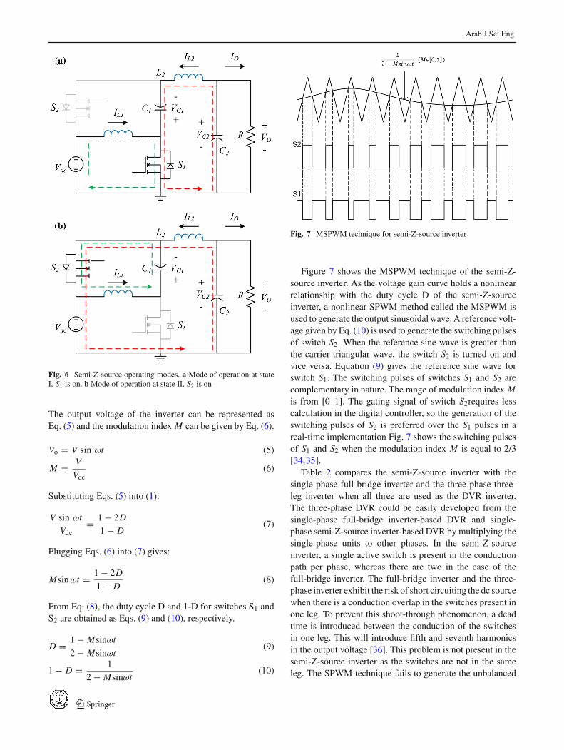
Figure 6 shows the equivalent circuit of the semi-Z-sourceinverter for the two states of operation in one switchingperiod. Figure 6a shows themode of operation at state Iwherethe switch S1 is conducting. During this mode of operation,the input dc source and the capacitor C1 charge the inductorsL1 and L2. Figure 6b shows the mode of operation at stateII where switch S2 is conducting. During this mode of oper-ation, the two inductors act as the source and the inductorcurrent is decreased. The steady-state equations of the semi-Z-source inverter are given in Eqs. (1)–(4), assuming thedirection of the inductor current references and the capacitorvoltage references as given in Fig. 6a, b.
VoVdc
= 1 − 2D
1 − D(1)
Vc1 = D
1 − DVdc (2)
IL2 = −Io (3)
IL1 = − D
1 − DIo (4)
123
Arab J Sci Eng
Fig. 6 Semi-Z-source operating modes. a Mode of operation at stateI, S1 is on. bMode of operation at state II, S2 is on
The output voltage of the inverter can be represented asEq. (5) and the modulation index M can be given by Eq. (6).
Vo = V sin ωt (5)
M = V
Vdc(6)
Substituting Eqs. (5) into (1):
V sin ωt
Vdc= 1 − 2D
1 − D(7)
Plugging Eqs. (6) into (7) gives:
Msinωt = 1 − 2D
1 − D(8)
From Eq. (8), the duty cycle D and 1-D for switches S1 andS2 are obtained as Eqs. (9) and (10), respectively.
D = 1 − Msinωt
2 − Msinωt(9)
1 − D = 1
2 − Msinωt(10)
Fig. 7 MSPWM technique for semi-Z-source inverter
Figure 7 shows the MSPWM technique of the semi-Z-source inverter. As the voltage gain curve holds a nonlinearrelationship with the duty cycle D of the semi-Z-sourceinverter, a nonlinear SPWM method called the MSPWM isused to generate the output sinusoidalwave.A reference volt-age given by Eq. (10) is used to generate the switching pulsesof switch S2. When the reference sine wave is greater thanthe carrier triangular wave, the switch S2 is turned on andvice versa. Equation (9) gives the reference sine wave forswitch S1. The switching pulses of switches S1 and S2 arecomplementary in nature. The range of modulation index Mis from [0–1]. The gating signal of switch S2requires lesscalculation in the digital controller, so the generation of theswitching pulses of S2 is preferred over the S1 pulses in areal-time implementation Fig. 7 shows the switching pulsesof S1 and S2 when the modulation index M is equal to 2/3[34,35].
Table 2 compares the semi-Z-source inverter with thesingle-phase full-bridge inverter and the three-phase three-leg inverter when all three are used as the DVR inverter.The three-phase DVR could be easily developed from thesingle-phase full-bridge inverter-based DVR and single-phase semi-Z-source inverter-based DVR by multiplying thesingle-phase units to other phases. In the semi-Z-sourceinverter, a single active switch is present in the conductionpath per phase, whereas there are two in the case of thefull-bridge inverter. The full-bridge inverter and the three-phase inverter exhibit the risk of short circuiting the dc sourcewhen there is a conduction overlap in the switches present inone leg. To prevent this shoot-through phenomenon, a deadtime is introduced between the conduction of the switchesin one leg. This will introduce fifth and seventh harmonicsin the output voltage [36]. This problem is not present in thesemi-Z-source inverter as the switches are not in the sameleg. The SPWM technique fails to generate the unbalanced
123

Arab J Sci Eng
Table 2 comparison between single-phase full-bridge inverter, three-phase inverter and semi-Z-source inverter
Sl. no. Parameters Single-phase full-bridge inverter Three- phase three-leg inverter Semi-Z-sourceinverter
1 Nature of the inverter Buck Buck Buck
2 No. of switches per phase 4 2 2
3 No. of active switches in thecurrent path per phase
2 1 1
4 No. of reactive components perphase
2 2 4
5 Generation of unbalanced outputvoltage when the sags arenon-symmetrical
Possible Difficult Possible
6 Need for filter Yes Yes No
7 Phase shift in the output voltagedue to filter
Yes Yes No
8 Risk of short circuit condition dueto conduction overlap of switchesin same leg
Yes Yes No
9 Need of dead time control Yes Yes No
10 Control Complex with dead time controland adaptive phase shiftcompensation
Complex with dead time controland adaptive phase shiftcompensation. For unbalancedoutput voltages, space vectormodulation is preferred
Simple
11 No. of ADC per phase 3 3 2
12 No. of voltage sensing element 3 3 2
13 Voltage overshoot due to LC filterparameters
Yes Yes No
three-phase output voltage in the three-phase inverter whencompared to the full-bridge inverter and the semi-Z-sourceinverter. Since most of the sags and swells are unbalanced,this provides limitations to the three-phase inverter-basedDVR during unbalanced voltage sags and swells [37]. Dur-ing the transient operation of the DVR, the load terminalsexperience a very large voltage overshoot depending on theLC filter parameters. This may affect the DVR operation andmay even result in the tripping of the load [38]. The absenceof the filter circuit makes the semi-Z-source inverter-basedDVR free from such voltage overshoots. In the literature [35],it is clearly mentioned that the cost of the semi-Z-sourceinverter is less than the single-phase full-bridge inverter. Inthe DVRs based on the full-bridge inverter and the three-phase inverter, an additional analogue-to-digital converter(ADC) and the voltage sensing element are required to com-pare the inverter output voltage and the reference voltagefor removing the phase shift caused by the filters. This willincrease the capital cost of the full-bridge inverter and thethree-phase inverter-based DVRs compared to the semi-Z-source inverter-basedDVR. The heat sinks, optocouplers andthe driver circuits associated with the additional switches inthe full-bridge inverter also add to the cost.
3 Proposed DVR Topology with Semi-Z-SourceInverter
Figure 8 displays the single-phase representation of the pro-posed topology of the DVR with the semi-Z-source invertermarked by the dashed line box. The topology consists of a dcvoltage source (Vdc), semi-Z-source inverter and an injectiontransformer. The transformer provides the voltage boosting
Fig. 8 Proposed DVR topology with semi-Z-source inverter
123

Arab J Sci Eng
function and electrical isolation. The secondary of the injec-tion transformer connects the DVR in series with the supplyand the load. Here, in this paper, the transformer providesonly electrical isolation. According to the sag depth and thephase jump, the semi-Z-source inverter injects the missingvoltage through the injection transformer, and thus, the loadprofile is restored.
For cost-effectiveness, the common practice in DVR tech-nology is to design the DVR with 50% voltage injectioncapability as most of the sags are limited to 50% sag depth[6,39]. The dc source Vdc is selected as 50% of the nominalline voltage peak value. A safety margin is provided to pre-vent the reverse power flow through the anti-parallel diodesof the switches in the inverter [40]. In the proposed topology,the margin is chosen as 20%.
This paper uses the missing voltage technique describedin [41] to detect the sag and to evaluate the missing volt-age. During the voltage sag conditions, the missing voltageis determined by subtracting the actual supply instantaneousvoltage (vsupply) from the desired load instantaneous voltage(vload,ref ). The reference for DVR voltage is generated withthe help of the phase-locked loops (PLL). The missing volt-age (vmv) obtained from Eq. (11) is taken as the reference forthe DVR output voltage (vDVR). The semi-Z-source inverteroutputs the missing voltage, and it is injected to regulate theload profile.
vmv = vload,ref − vsupply (11)
Here, in this single-phase DVR application, the voltage vmv
determines the range of the duty cyclesDand1-Dof the semi-Z-source inverter switches S1 and S2, respectively. Underany sag conditions, the two switches S1 and S2 are operatedin complementary manner such that the load voltage (vload)matches the load reference voltage (vload,ref ). The semi-Z-source inverter output (vinv) is equal to vDVR since the turnsratio ’n’ of the injection transformer is 1:1. The DVR outputvoltage vDVRis equal to the missing voltage vmv when theload voltage Vload is restored to 100%. The modulation indexM is dependent on the peak value of the voltage to be injected(Vmv) and Vdc.
vmv = Vmv sinωt (12)
M = Vmv
Vdc(13)
Equations (5) and (6) can be co-related with Eqs. (12) and(13), respectively. The duty cycle D and 1-D of the switchesS1 and S2 are determined in the sameway as given by Eqs. (9)and (10), respectively. The vmv decides the range of modu-lation index M and the duty cycle D and 1-D of the switchesS1 and S2, respectively. With MSPWM, the semi-Z-sourceinverter gives the sinusoidal output voltage with permissible
Fig. 9 Load compensation using transformerless DVR based on semi-Z-source inverter
harmonic content. The harmonics present in the semi-Z-source inverter output voltage are within the limits given byIEEEStandard 519-2014. The sinusoidal output voltage fromthe semi-Z-source inverter is injected in serieswith the supplyand load with the help of an injection transformer. By select-ing the injection transformer with appropriate turns ratio ‘n’,the voltage requirement of the semi-Z-source inverter can bereduced further.
The presence of only a permissible amount of harmon-ics in the output voltage, even without any additional filtercomponents, makes the semi-Z-source inverter suitable forthe transformerless topology of the DVR. Figure 9 showsthe load voltage compensation during the sag condition fora single-phase transformerless DVR based on the semi-Z-source inverter. The THD of the load voltage is determined tobe only 0.82%without using any of the filtering schemes. Thefilter circuit is indispensable in a full-bridge inverter-basedDVR system. The absence of additional filter componentsand the Z-source network present in the ac side can be con-sidered as themerits of the semi-Z-source inverter when usedin the DVR system.
4 DVR Controller and Modulation Technique
The small-signal modelling of the semi-Z-source inverter isperformed by defining the inductor currents and the capacitorvoltages as the state variables as given by:
x (t) = [iL1 (t) iL2 (t) vC1 (t) vC2 (t)
]T(14)
For the small-signal modelling of the semi-Z-source con-verter, the passive components in the impedance networkare assumed to be lossless. The on resistance and the for-ward voltage drop of the switches S1 and S2 are neglected.The input voltage Vdc is an independent voltage source,
123

Arab J Sci Eng
Fig. 10 Feedforward control block diagram
and the load is taken as resistive (R) [42,43]. To derive thesmall-signal model, perturbations vdc(t)and d(t)are addedto the input voltage and the duty cycle and are given byvdc(t) = Vdc + vdc(t) and d(t) = D + d(t), respectively.
The variation in the state variables due to the perturbations isgiven by x(t) = X + x . The small-signal state equations ofthe semi-Z-source inverter are given by the following equa-tions (see “Appendix”):
sL1 · iL1 (s) = (D − 1) vC1 (s)
+ Dvdc (s) + Vdc(1 − D)
d (s) (15)
sL2 · iL2 (s) = −RiL2 (s) + DvC1 (s)
+ (D − 1) vdc (s) + Vdc(1 − D)
d (s) (16)
sC1 · vC1 (s) = (1 − D) iL1 (s)
+ DiL2 (s) + IL2
(1 − D)d (s) (17)
sC2 · vC2 (s) = iL2 (s) (18)
The output voltage vinv of the semi-Z-source inverter is thesame as the capacitor voltage vC2 . The small-signal expres-sion for the capacitor voltage vC2 can be expressed as thelinear combination of input voltage and duty cycle perturba-tion as:
vC2 (s) = Gvdc (s) · vdc (s) + Gvd (s) · d (s) (19)
In Eq. (19), Gvdc (s) and Gvd (s) represent the input-to-capacitor voltage transfer function and control-to-capacitorvoltage transfer function and are given by Eqs. (20) and (21),respectively:
Gvdc (s) = 1
C2s
[(D − 1) L1C1s2 + D2 (1 − D) − (1 − D)3
L1L2C1s3 + RL1C1s2 + ((1 − D)2 L2 − D2L1
)s + R (1 − D)2
]
(20)
Gvd (s) = 1
C2s
⎡
⎣
(D + 1
1−D L1C1s2 + (1 − D))Vdc + D
1−D L1 IL2s
L1L2C1s3 + RL1C1s2 + ((1 − D)2 L2 − D2L1
)s + R (1 − D)2
⎤
⎦ (21)
Here, in the proposed DVR topology, the input voltage Vdc isconsidered as a stiff dc source. So, the output voltage expres-sion is reduced to:
vC2 (s) = Gvd (s) · d (s) (22)
4.1 Feedforward Control of the Semi-Z-SourceInverter-Based DVR
Figure 10 shows the feedforward control block diagramof thesemi-Z-source inverter-based DVR. Robustness and simplic-ity are the key advantages of the feedforward voltage controlin the DVR system [17]. A reference load voltage vload,refis generated, and the instantaneous difference between theactual supply vsupply and reference load voltage vload,ref isdetermined. This difference is equal to zero when there is noPQ problem, assuming the system is lossless. During the sagevents, this difference provides the missing voltage vmv asgiven in Eq. (11), which is the voltage to be injected by theDVR.
In the feedforward control,vmv is scaled by a scaling factorequal to the dc-link voltage (Vdc) to obtain the scaledmissingvoltage (vmv,scaled) similar to the term Msinωt given in thedescription of the MSPWM technique. This scaled missing
123

Arab J Sci Eng
Fig. 11 Modified feedback control block diagram
voltage (vmv,scaled) is modified in the digital controller toobtain the d (s) , which is analogous to the term given byEq. (9). Due to the relationship given by Eq. (23), the outputof the block Gvd (s) is the inverter voltage,vinv
Gvd (s) = vC2(s)
d(s)(23)
4.2 Modified Feedback Control of the Semi-Z-SourceInverter-Based DVR
In this modified feedback control of the proposed DVRtopology, the DVR voltage (vDVR) is taken as the feedbackparameter. Generation of the missing voltage vmv is the sameas that in the feedforward control. In this modified feedbackcontrol, the semi-Z-source inverter is controlled in such amanner that at any instant the DVR voltage (vDVR) shouldmatch the missing voltage,vmv. The missing voltage vmv isset as the reference for the DVR voltage (vDVR), and the errorbetween them (verr) is corrected using the PI controller.
Figure 11 shows the modified feedback control block dia-gram for the proposed semi-Z-source inverter-based DVR.Here, as the injection transformer only provides galvanic iso-lation, vDVR and vinv are the same voltages. The PI controllerhandles any error between vDVR and vmv given by Eq. (24)[17]. Furthermore, Hv (s) demonstrates the transfer functionof the PI controller given by Eq. (25) and its output vpi issimilar to the Msin ωt term given in the description of theMSPWM technique. From the PI controller output vpi, thesignal d (s) is obtained using Eq. (9).
verr = vmv − vDVR (24)
Hv (s) = Kp + Ki
s(25)
The modified feedback controller also follows Eq. (23), andthe inverter output voltage vinv is obtained. A gain ‘k’ equalto the turns ratio ‘n’ of the injection transformer (1 in thiscase) is given to the inverter voltage vinv to obtain the DVRvoltage vDVR. The voltage vDVR is compared with the actual
reference voltage vmv, and the feedback loop attempts toreduce the error to zero. This control method of the proposedDVR assures the proper tracking of the reference voltage bythe semi-Z-source inverter.
5 Design and Simulation Results
The performance of the semi-Z-source inverter DVR andits control technique have been verified using MATLAB/Simulink. The simulation parameters of the single-phasesemi-Z-source inverter-based DVR are given in Table 3.The missing voltage technique is used to detect the voltagesag [41]. The in-phase compensation method is adopted asthe compensation technique. The feedforward and modifiedfeedback control strategies are utilised for the simulation,and the missing voltage vmv is taken as the reference for theinjected voltage vDVR.
Considering the maximum injection of 50% of the single-phase rms voltage, (Vsupply) and the 20% extra given in the dcsource voltage (Vdc), the maximum modulation index Mmax
is derived as 0.81 from:
Mmax = 0.5 ∗ √2 ∗ VsupplyVdc
(26)
Table 3 Simulation parameters
Parameters Values
Rated voltage andfrequency
230 V and 50 Hz
Load 800 + j600 VA
Injection transformer 1:1230 V, 1.6 kVA
Semi-Z-source Inverter Dc-link voltage, Vdc 200 V
Switching frequency, fsw 50 kHz
Capacitor C1 and C2 3.9 µF
Inductor L1 and L2 320 µH
123

Arab J Sci Eng
Fig. 12 Compensation using feedforward control. a Sag initiation at positive going zero-crossing, b sag initiation at negative going zero-crossing,c sag initiation at positive peak, d sag initiation at negative peak
For obtaining the output voltage range of (+ 115 to− 115V),the duty cycle D of switch S1 is changed from 0.16 to 0.644according to the voltage ratio given in Fig. 5. By varying theduty cycle D from 0.16 to 0.5, the positive output voltagefor the maximum injection is obtained. The negative outputvoltage is obtained when the duty cycle D is varied from 0.5to 0.644. The inductor and capacitor values of the semi-Z-source inverter are designed by considering the maximuminjection capability.
All the simulation results given in this paper show theresponse of the DVR system for 40% sag in the supply volt-age. The DVR system is simulated to protect a linear loadof 1 kVA. The four worst cases of the point on wave of saginitiation, namely (a) sag initiation at positive going zero-crossing, (b) sag initiation at negative going zero-crossing,(c) sag initiation at the positive peak and (d) sag initiationat the negative peak, are simulated with system parameters
given in Table 3. Figure 12 shows the supply voltage, DVRinjected voltage and load voltage when the proposed single-phase semi-Z-source inverter-based DVR is controlled usingthe feedforward control scheme given in Fig. 10.As depicted,whenever the sag event begins, the semi-Z-source inverter isoperated to inject the missing voltage in series with the sup-ply and the load. Irrespective of the sag in the supply voltage,the feedforward controlled DVR restores the load voltagewithout any delay by injecting the appropriate voltage by thesemi-Z-source inverter.
Figure 13 illustrates the corresponding waveforms for thesame four worst cases of sag conditions when the semi-Z-source inverter-based DVR is modified feedback controlledusing the PI controller. The same system parameters givenin Table 3 are used for the simulation of the modified feed-back controlled proposed single-phase DVR with Kp andKivalues equal to 0.017 and 1.1, respectively. A half-cycle
123

Arab J Sci Eng
Fig. 13 Compensation using feedback control. a Sag initiation at positive going zero-crossing, b sag initiation at negative going zero-crossing, csag initiation at positive peak, d sag initiation at negative peak
compensation delay is experienced from the point of sagoccurrence in this control.
In both the feedforward and modified feedback controlof the proposed DVR, the DVR output vDVR tries to matchthe missing voltage, vmv. The reference voltage is trackedexactly by the semi-Z-source inverter output voltage as givenin Fig. 14. The efficiency of the semi-Z-source inverter formitigating the sag of depth 40% is found to be around 98%from the simulation studies. The steady-state THD analysisof the load voltage for the four worst cases of sags underthe feedforward and feedback control is given in Table 4.From time 0.16 s, seven cycles of the load voltage Vload areconsidered for the THD analysis.
A comparison study of the efficiency of the semi-Z-source inverter-basedDVRand the full-bridge inverter-basedDVR is also conducted for different sag depths. The miss-ing voltage vmv and the modulation index M hold a linear
Fig. 14 Magnitude and phase comparison between reference voltageand semi-Z-Source inverter output voltage
123

Arab J Sci Eng
Table 4 Load voltage THDanalysis
Different cases of point on wave of sag initiation THD of Vload
Feedforward control Feedback control
Sag initiation at positive going zero-crossing 0.73 0.67
Sag initiation at negative going zero-crossing 0.73 0.73
Sag initiation at positive peak 0.73 0.67
Sag initiation at negative peak 0.73 0.81
Fig. 15 Efficiency curve
Fig. 16 Load voltage THD versus sag depth
relationship, as given by Eq. (13). The efficiency curve ofthe DVR based on the semi-Z-source inverter and the full-bridge inverter is plotted against themodulation indexM andis illustrated in Fig. 15. The efficiency of the semi-Z-sourceinverter is comparable with that of the full-bridge inverter.For sag depths up to 50% of the nominal line voltage, theTHD of the load voltage is compared for the semi-Z-sourceinverter-based DVR and the full-bridge inverter-based DVR.As shown in Fig. 16, without using any filtering scheme,
the THD of the semi-Z-source inverter-based DVR is betterthan the full-bridge inverter-based DVR with inverter-sidefiltering. Altogether, considering the cost, efficiency, THDand performance of the semi-Z-source inverter, it is a betteralternative to the full-bridge inverter in DVR applications.
6 Conclusion
This technical note proposes a novel topology of the single-phase DVR based on the semi-Z-source inverter and itsfeedforward and modified feedback control strategies. Thereduced size of the Z-source network, same output voltagerange as the full-bridge inverter with a reduced number ofswitches, the absence of filter components and only a sin-gle switch in the current path are some of the advantages ofthe semi-Z-source inverter. The proposed DVR is controlledusing both the feedforward and themodified feedback controlscheme. The small-signal modelling of the semi-Z-sourceinverter, the feedforward and the modified feedback controlscheme for the proposed semi-Z-source inverter-based DVRare discussed in detail in Sect. 4. Both the control schemescompensate for the upstreamsag conditions efficientlywithin10 ms. The feasibility of the proposed topology in restoringthe load voltage under sag conditions has been verified in theMATLAB/Simulink environment. The simulation results andTable 4 validate the efficacy of the new topology of the DVR.
Acknowledgements The authors thank the anonymous reviewers forgiving their valuable comments and helping us to improve the qualityof the paper.
APPENDIX
Small-signal modelling of the semi-Z-source inverter
The inductor currents and capacitor voltages are defined asstate variables which is already given in the paper as equation(14)
For state Imodeof operation of the semi-Z-source inverter,the differential equations governing the systemcan bewritten
123

Arab J Sci Eng
in the form x(t) = A1.x(t) + B1.u as given in equation (27)
d
dt
⎡
⎢⎢⎣
iL1(t)iL2(t)vC1(t)vC2(t)
⎤
⎥⎥⎦ =
⎡
⎢⎢⎢⎣
0 0 0 00 −R
L2
1L2
00 1
C10 0
0 1C2
0 0
⎤
⎥⎥⎥⎦
⎡
⎢⎢⎣
iL1(t)iL2(t)vC1(t)vC2(t)
⎤
⎥⎥⎦
+
⎡
⎢⎢⎣
1L1
000
⎤
⎥⎥⎦
[Vdc
](27)
For state II mode of operation of the semi-Z-source inverter,the differential equations governing the systemcan bewrittenin the form x(t) = A2.x(t) + B2.u as given in equation (28)
d
dt
⎡
⎢⎢⎣
iL1(t)iL2(t)vC1(t)vC2(t)
⎤
⎥⎥⎦ =
⎡
⎢⎢⎢⎣
0 0 −1L1
00 −R
L20 0
1C1
0 0 00 1
C20 0
⎤
⎥⎥⎥⎦
⎡
⎢⎢⎣
iL1(t)iL2(t)vC1(t)vC2(t)
⎤
⎥⎥⎦
+
⎡
⎢⎢⎣
0− 1
L2
00
⎤
⎥⎥⎦
[Vdc
](28)
Considering high switching frequency, the dc steady stateequations describing the semi-Z-source converter can bewritten as
0 = (DA1 + (1 − D) A2) X + (DB1 + (1 − D) B2)U (29)
By solving (29), the steady state equation of the semi-Z-source inverter given by equations (1) - (4) is obtained.
To derive the small-signal model, perturbations are addedto the input voltage and duty cycle as vdc(t) and d(t) respec-tively.
In general, small-signal state space equations representedby
ˆX = (DA1 + (1 − D) A2) .X + (DB1 + (1 − D) B2) .U
+ [(A1 − A2) X + (B1 − B2)U ] d(t)
is given by equation (30)
ˆX =
⎡
⎢⎢⎢⎣
0 0 D−1L1
00 −R
L2
DL2
0−DC1
DC1
0 00 1
C20 0
⎤
⎥⎥⎥⎦
.X +
⎡
⎢⎢⎣
DL1D−1L2
00
⎤
⎥⎥⎦ .U
+
⎡
⎢⎢⎢⎣
0 0 1L1
00 0 1
L20
−1C1
1C1
0 00 0 0 0
⎤
⎥⎥⎥⎦
.X +
⎡
⎢⎢⎣
1L11L2
00
⎤
⎥⎥⎦ .U (30)
After Laplace transformation of equation (30), equations (15)– (18) are obtained.
The control-to-capacitor voltage transfer function Gvd (s)is obtained by substituting vdc = 0 in equations (15)-(18).The equations reduce to
sL1.iL1(s)|Vdc(s)=0 = (D − 1) .vC1(s)
+ Vdc(1 − D)
d(s) (31)
sL2.iL2(s)|Vdc(s)=0 = −R.iL2(s) + DvC1(s)
+ Vdc(1 − D)
d(s) (32)
sC1.vC1(s)|Vdc(s)=0 = (1 − D) .iL1(s) + D.iL2(s)
+ iL2(1 − D)
d(s) (33)
sC2.vC2(s)|Vdc(s)=0 = iL2(s) (34)
From the equations (31) – (34), vC2(s) is found out as theproduct of d(s) andGvd (s)whereGvd (s) is givenby equation(21)
References
1. Brumsickle, W.E.; Schneider, R.S.; Luckjiff, G.A.; Divan, D.M.;McGranaghan,M.F.: Dynamic sag correctors: cost-effective indus-trial power line conditioning. IEEE Trans. Ind. Appl. 37(1),212–217 (2001)
2. Vilathgamuwa,M.; Ranjith Perera, A. A. D.; Choi, S. S.; Tseng, K.J.: Control of energy optimized dynamic voltage restorer. In: Indus-trial Electronics Society, 1999. IECON’99 Proceedings. The 25thAnnual Conference of the IEEE, San Jose, CA, vol. 2, pp. 873–878(1999)
3. Daehler, P.; Affolter, R.: Requirements and solutions for dynamicvoltage restorer, a case study. In: 2000 IEEE Power EngineeringSocietyWinterMeeting.Conference Proceedings, vol. 4, pp. 2881–2885 (2000)
4. Dugan, R.C.; Dugan, R.C. (eds.): Electrical Power Systems Qual-ity, 2nd edn. McGraw-Hill, New York (2003)
5. Zhan, C.; Arularnpalam, A.; Ramachandaramurthy, V. K.; Fitzer,C.; Barnes, A.; Jenkins, N.: Dynamic voltage restorer based on 3-dimensional voltage space vector PWM algorithm. In: 2001 IEEE32nd Annual Power Electronics Specialists Conference, Vancou-ver, BC, vol. 2, pp. 533–538 (2001)
6. Abi-Samra, N.; Carnovale, D.; Sundaram, A.; Malcolm, W.: Therole of the distribution system dynamic voltage restorer in enhanc-ing the power at sensitive facilities. In: Wescon/96, Anaheim, CA,pp. 167–181 (1996)
7. Woodley, N. H.: Field experience with Dynamic Voltage Restorer(DVRTMMV) systems. In: 2000 IEEE Power Engineering SocietyWinter Meeting. Conference Proceedings, vol. 4, pp. 2864–2871(2000)
8. Carlos, G.; Jacobina, C.; Santos, E.: Investigation on dynamicvoltage restorers with two DC-links and series converters forthree-phase four-wire systems. IEEE Trans. Ind. Appl. vol. 52,pp.1608–1620 (2015)
9. Komurcugil, H.; Biricik, S.: Time-varying and constant switchingfrequency-based sliding-mode control methods for transformerless
123

Arab J Sci Eng
DVR employing half-bridgeVSI. IEEETrans. Ind. Electron. 64(4),2570–2579 (2017)
10. Sasitharan, S.; Mishra, M.K.; Kalyan Kumar, B.; Jayashankar, V.;Rating and design issues of DVR injection transformer. In: 2008Twenty-Third Annual IEEE Applied Power Electronics Confer-ence and Exposition. Austin, TX, pp. 449–455 (2008)
11. Woodley, N.H.; Morgan, L.; Sundaram, A.: Experience with aninverter-based dynamic voltage restorer. IEEE Trans. Power Deliv.14(3), 1181–1186 (1999)
12. Nielsen, J.G.; Blaabjerg, F.: A detailed comparison of systemtopologies for dynamic voltage restorers. IEEE Trans. Ind. Appl.41(5), 1272–1280 (2005)
13. Kanjiya, P.; Singh, B.; Jayaprakash, P.: A robust control algorithmfor self supported dynamic voltage restorer (DVR). In: India Inter-national Conference on Power Electronics 2010 (IICPE2010), NewDelhi, pp. 1–8 (2011)
14. Ghosh, A.G.; Jindal, A.K.; Joshi, A.: Design of a capacitor-supported dynamic voltage restorer (DVR) for unbalanced anddistorted loads. IEEE Trans. Power Deliv. 19(1), 405–413 (2004)
15. Kanjiya, P.; Singh, B.; Chandra, A.; Al-Haddad, K.: SRF the-ory revisited; to control self-supported Dynamic Voltage Restorer(DVR) for unbalanced and nonlinear loads. IEEE Trans. Ind. Appl.49(5), 2330–2340 (2013)
16. Meyer, C.; De Doncker, R.W.; Li, Y.W.; Blaabjerg, F.: Optimizedcontrol strategy for a medium-voltage DVR; Theoretical investiga-tions and experimental results. IEEE Trans. Power Electron. 23(6),2746–2754 (2008)
17. GodskNielsen, J.:Design and control of a dynamic voltage restorer.In: Institute of Energy Technology, Aalborg University, Aalborg(2002)
18. Jing, W.; Aiqin, X.; Yueyue, S.: A survey on control strategies ofdynamic voltage restorer. In: 2008 13th International Conferenceon Harmonics and Quality of Power, Wollongong, NSW, pp. 1–5(2008)
19. Chiang, H.-K.; Lin, B.-R.; Wu, K.-W.: Study of dynamic voltagerestorer under the abnormal voltage conditions. In: 2005 Interna-tional Conference on Power Electronics andDrives Systems, KualaLumpur, pp. 308–312 (2005)
20. Ho, C.N.M.; Chung, H.S.H.: Fast transient control of single-phasedynamic voltage restorer (DVR) without external DC source. In:2006 37th IEEE Power Electronics Specialists Conference, Jeju,pp. 1–7 (2006)
21. Silva, S.M.; da Silveira, S.E.; de SouzaReis,A.; CardosoFilho,B.J.:Analysis of a dynamic voltage compensator with reduced switch-count and absence of energy storage system. IEEETrans. Ind.Appl.41(5), 1255–1262 (2005)
22. Fang, M.; Gardiner, A. I.; MacDougall, A.; Mathieson, G. A.:A novel series dynamic voltage restorer for distribution systems.In: 1998 International Conference on Power System Technology,1998. Proceedings. POWERCON’98, Beijing, vol. 1, pp. 38–42(1998)
23. Bae, B.Y.; Lee, D.K.; Han, B.M.: Development of high-performance single-phase line-interactive dynamic voltagerestorer. In: 2007 Australasian Universities Power EngineeringConference, Perth, WA, pp. 1–6 (2007)
24. Zhan, C.; et al.: Dynamic voltage restorer based on voltage-space-vector PWM control. IEEE Trans. Ind. Appl. 37(6), 1855–1863(2001)
25. Ramachandaramurthy, V.K.; Fitzer, C.; Arulampalam, A.; Zhan,C.; Barnes,M.; Jenkins, N.: Control of a battery supported dynamicvoltage restorer. IEE Proc. Gener. Transm. Distrib. 149(5), 533(2002)
26. Arulampalam, A.; Jenkins, N.; Zhan, C.; et al.: Four-wire dynamicvoltage restorer based on a three-dimensional voltage space vector
pwm algorithm. IEEE Trans. Power Electron. 18(4), 1093–1102(2003)
27. Loh, P.C.; Vilathgamuwa, D.M.; Tang, S.K.; Long, H.L.: Multi-level dynamic voltage restorer. In: 2004 International Conferenceon Power System Technology, 2004. PowerCon 2004, vol. 2, pp.1673–1678 (2004)
28. Sabahi, M.; Kangarlu, M.F.; Babaei, E.: Dynamic voltage restorerbased on multilevel inverter with adjustable dc-link voltage. IETPower Electron. 7(3), 576–590 (2014)
29. Yin, Z.; Han,M.; Zhou, L; Yu, K.: Project study of dynamic voltagerestorer. In: IEEE/PES Transmission and Distribution Conferenceand Exposition: Asia and Pacific. Dalian, 2005, pp. 1–8 (2005)
30. Wang, S.; Tang, G.; Yu, K.; Zheng, J.: Modeling and control of anovel transformer-less dynamic voltage restorer based on H-bridgecascaded multilevel inverter. In: 2006 International Conference onPower System Technology, Chongqing, pp. 1–9 (2006)
31. Li, B.H.; Choi, S.S.; Vilathgamuwa, D.M.: Design considerationson the line-side filter used in the dynamic voltage restorer. IEEProc. Gener. Transm. Distrib. 148(1), 1 (2001)
32. Massoud, A.M.; Ahmed, S.; Enjeti, P.N.; Williams, B.W.: Eval-uation of a multilevel cascaded-type dynamic voltage restoreremploying discontinuous space vector modulation. IEEE Trans.Ind. Electron. 57(7), 2398–2410 (2010)
33. Banaei, M. R.; Salary, E.: New multilevel inverter with reductionof switches and gate driver. In: 2010 18th Iranian Conference onElectrical Engineering, Isfahan, Iran, pp. 784–789 (2010)
34. Cao, D.; Jiang, S.; Yu, X.; Peng, F.Z.: Low-cost semi-Z-sourceinverter for single-phase photovoltaic systems. IEEE Trans. PowerElectron. 26(12), 3514–3523 (2011)
35. Mekhilef, S.; Ahmed, T.: Semi-Z-source inverter topology for grid-connected photovoltaic system. IET Power Electron. 8(1), 63–75(2015)
36. Hur, N.; Nam, K.;Won, S.: A two-degrees-of-freedom current con-trol scheme for deadtime compensation. IEEETrans. Ind. Electron.47(3), 557–564 (2000)
37. Babaei, E.; Kangarlu, M. F.: Comparison four topologies for three-phase dynamic voltage restorer. In:2015 International Conferenceon Renewable Energy Research and Applications (ICRERA),Palermo, pp. 1527–1532 (2015)
38. Kim, H.; Kim, J.-H.; Sul, S.-K.: A design consideration of outputfilters for dynamic voltage restorers. In: 2004 IEEE 35th AnnualPower Electronics Specialists, vol. 6, pp. 4268–4272 (2004)
39. Woodley, N.H.; Sundaram, A.; Holden, T.; Einarson, T.C.: Fieldexperience with the new platform-mounted DVRTM. In: PowerCon2000. 2000 International Conference on Power System Technol-ogy. Proceedings, Perth, WA, vol. 3, pp. 1323–1328 (2000)
40. Morán, L.; Dixon, J.: 41—active filters. In: Rashid, M.H. (eds.) InPower Electronics Handbook (3rd edn), Butterworth-Heinemann,Boston, pp. 1193–1228. ISBN: 9780123820365 (2011)
41. Tunaboylu, N. S.; Collins, E. R.; Chaney, P. R.: Voltage disturbanceevaluation using the missing voltage technique. In: Proceedingsof the 8th International Conference on Harmonics and Quality ofPower, Athens, vol. 1, pp. 577–582 (1998)
42. Liu, J.; Hu, J.; Xu, L.: Dynamic modeling and analysis of Z-sourceconverter-derivation of AC small signal model and design-orientedanalysis. IEEE Trans. Power Electron. 22(5), 1786–1796 (2007)
43. Vahedi, H.; Shojaei, A.A.; Chandra, A.; Al-Haddad, K.: Five-levelreduced-switch-count boost PFC rectifier with multicarrier PWM.IEEE Trans. Ind. Appl. 52(5), 4201–4207 (2016)
123

![PERFORMANCE OF DVR AND IDVR FOR VOLTAGE ...Power Quality Improvement Using Multi -Level Inverter Based DVR and DSTATCOM Using Neuro -Fuzzy Controller. [3] Power Quality Improvement](https://static.fdocuments.in/doc/165x107/5ed31f7b2c1fe74f476f3361/performance-of-dvr-and-idvr-for-voltage-power-quality-improvement-using-multi.jpg)