
Single-Channel, 12-/16-Bit Programmable Current Output · PDF fileRegister DAC Input Register...
65
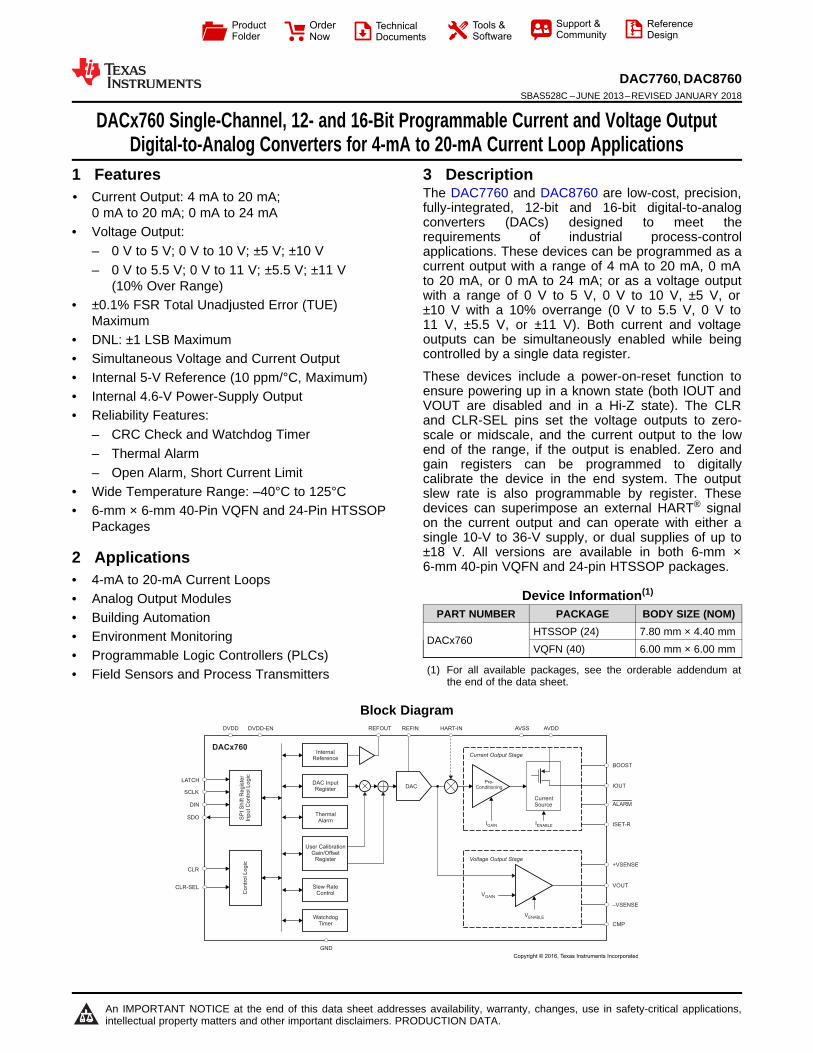
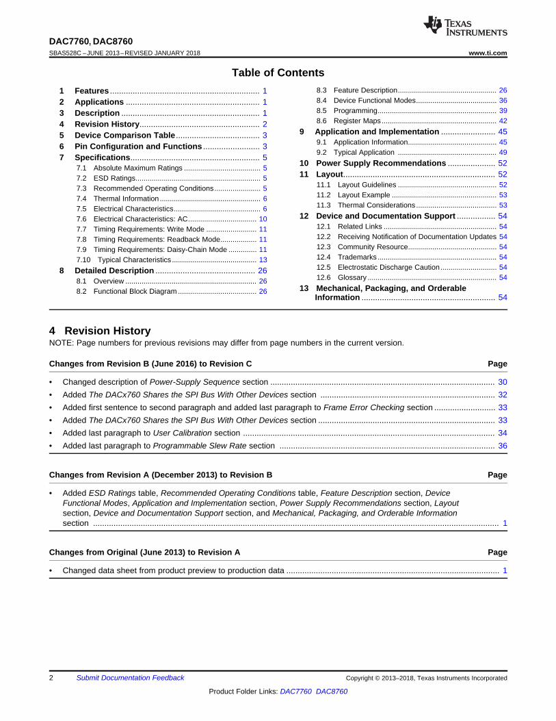
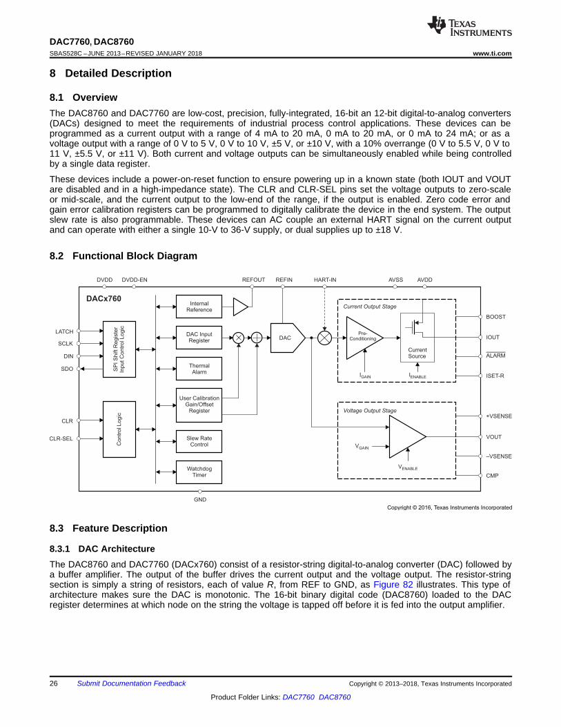
DAC GND DACx760 AVDD DVDD-EN AVSS DVDD Pre- Conditioning Current Source I ENABLE ISET-R I GAIN V GAIN V ENABLE Current Output Stage Voltage Output Stage Watchdog Timer Slew Rate Control User Calibration Gain/Offset Register DAC Input Register Thermal Alarm Internal Reference SPI Shift Register Input Control Logic Control Logic CMP –VSENSE +VSENSE VOUT IOUT ALARM BOOST REFOUT REFIN HART-IN LATCH SCLK DIN SDO CLR CLR-SEL Copyright © 2016, Texas Instruments Incorporated Product Folder Order Now Technical Documents Tools & Software Support & Community Reference Design An IMPORTANT NOTICE at the end of this data sheet addresses availability, warranty, changes, use in safety-critical applications, intellectual property matters and other important disclaimers. PRODUCTION DATA. DAC7760, DAC8760 SBAS528C – JUNE 2013 – REVISED JANUARY 2018 DACx760 Single-Channel, 12- and 16-Bit Programmable Current and Voltage Output Digital-to-Analog Converters for 4-mA to 20-mA Current Loop Applications 1 1 Features 1• Current Output: 4 mA to 20 mA; 0 mA to 20 mA; 0 mA to 24 mA • Voltage Output: – 0 V to 5 V; 0 V to 10 V; ±5 V; ±10 V – 0 V to 5.5 V; 0 V to 11 V; ±5.5 V; ±11 V (10% Over Range) • ±0.1% FSR Total Unadjusted Error (TUE) Maximum • DNL: ±1 LSB Maximum • Simultaneous Voltage and Current Output • Internal 5-V Reference (10 ppm/°C, Maximum) • Internal 4.6-V Power-Supply Output • Reliability Features: – CRC Check and Watchdog Timer – Thermal Alarm – Open Alarm, Short Current Limit • Wide Temperature Range: –40°C to 125°C • 6-mm × 6-mm 40-Pin VQFN and 24-Pin HTSSOP Packages 2 Applications • 4-mA to 20-mA Current Loops • Analog Output Modules • Building Automation • Environment Monitoring • Programmable Logic Controllers (PLCs) • Field Sensors and Process Transmitters 3 Description The DAC7760 and DAC8760 are low-cost, precision, fully-integrated, 12-bit and 16-bit digital-to-analog converters (DACs) designed to meet the requirements of industrial process-control applications. These devices can be programmed as a current output with a range of 4 mA to 20 mA, 0 mA to 20 mA, or 0 mA to 24 mA; or as a voltage output with a range of 0 V to 5 V, 0 V to 10 V, ±5 V, or ±10 V with a 10% overrange (0 V to 5.5 V, 0 V to 11 V, ±5.5 V, or ±11 V). Both current and voltage outputs can be simultaneously enabled while being controlled by a single data register. These devices include a power-on-reset function to ensure powering up in a known state (both IOUT and VOUT are disabled and in a Hi-Z state). The CLR and CLR-SEL pins set the voltage outputs to zero- scale or midscale, and the current output to the low end of the range, if the output is enabled. Zero and gain registers can be programmed to digitally calibrate the device in the end system. The output slew rate is also programmable by register. These devices can superimpose an external HART ® signal on the current output and can operate with either a single 10-V to 36-V supply, or dual supplies of up to ±18 V. All versions are available in both 6-mm × 6-mm 40-pin VQFN and 24-pin HTSSOP packages. Device Information (1) PART NUMBER PACKAGE BODY SIZE (NOM) DACx760 HTSSOP (24) 7.80 mm × 4.40 mm VQFN (40) 6.00 mm × 6.00 mm (1) For all available packages, see the orderable addendum at the end of the data sheet. Block Diagram
Transcript of Single-Channel, 12-/16-Bit Programmable Current Output · PDF fileRegister DAC Input Register...
DAC
GND
DACx760
AVDDDVDD-EN AVSSDVDD
Pre-Conditioning
CurrentSource
IENABLE ISET-RIGAIN
VGAIN
VENABLE
Current Output Stage
Voltage Output Stage
WatchdogTimer
Slew RateControl
User CalibrationGain/Offset
Register
DAC InputRegister
ThermalAlarm
InternalReference
SP
I S
hift R
egis
ter
Input C
ontr
ol Logic
Contr
ol Logic
CMP
–VSENSE
+VSENSE
VOUT
IOUT
ALARM
BOOST
REFOUT REFIN HART-IN
LATCH
SCLK
DIN
SDO
CLR
CLR-SEL
Copyright © 2016, Texas Instruments Incorporated
Product
Folder
Order
Now
Technical
Documents
Tools &
Software
Support &Community
ReferenceDesign
An IMPORTANT NOTICE at the end of this data sheet addresses availability, warranty, changes, use in safety-critical applications,intellectual property matters and other important disclaimers. PRODUCTION DATA.
DAC7760, DAC8760SBAS528C –JUNE 2013–REVISED JANUARY 2018
DACx760 Single-Channel, 12- and 16-Bit Programmable Current and Voltage OutputDigital-to-Analog Converters for 4-mA to 20-mA Current Loop Applications
1
1 Features1• Current Output: 4 mA to 20 mA;
0 mA to 20 mA; 0 mA to 24 mA• Voltage Output:
– 0 V to 5 V; 0 V to 10 V; ±5 V; ±10 V– 0 V to 5.5 V; 0 V to 11 V; ±5.5 V; ±11 V
(10% Over Range)• ±0.1% FSR Total Unadjusted Error (TUE)
Maximum• DNL: ±1 LSB Maximum• Simultaneous Voltage and Current Output• Internal 5-V Reference (10 ppm/°C, Maximum)• Internal 4.6-V Power-Supply Output• Reliability Features:
– CRC Check and Watchdog Timer– Thermal Alarm– Open Alarm, Short Current Limit
• Wide Temperature Range: –40°C to 125°C• 6-mm × 6-mm 40-Pin VQFN and 24-Pin HTSSOP
Packages
2 Applications• 4-mA to 20-mA Current Loops• Analog Output Modules• Building Automation• Environment Monitoring• Programmable Logic Controllers (PLCs)• Field Sensors and Process Transmitters
3 DescriptionThe DAC7760 and DAC8760 are low-cost, precision,fully-integrated, 12-bit and 16-bit digital-to-analogconverters (DACs) designed to meet therequirements of industrial process-controlapplications. These devices can be programmed as acurrent output with a range of 4 mA to 20 mA, 0 mAto 20 mA, or 0 mA to 24 mA; or as a voltage outputwith a range of 0 V to 5 V, 0 V to 10 V, ±5 V, or±10 V with a 10% overrange (0 V to 5.5 V, 0 V to11 V, ±5.5 V, or ±11 V). Both current and voltageoutputs can be simultaneously enabled while beingcontrolled by a single data register.
These devices include a power-on-reset function toensure powering up in a known state (both IOUT andVOUT are disabled and in a Hi-Z state). The CLRand CLR-SEL pins set the voltage outputs to zero-scale or midscale, and the current output to the lowend of the range, if the output is enabled. Zero andgain registers can be programmed to digitallycalibrate the device in the end system. The outputslew rate is also programmable by register. Thesedevices can superimpose an external HART® signalon the current output and can operate with either asingle 10-V to 36-V supply, or dual supplies of up to±18 V. All versions are available in both 6-mm ×6-mm 40-pin VQFN and 24-pin HTSSOP packages.
Device Information(1)
PART NUMBER PACKAGE BODY SIZE (NOM)
DACx760HTSSOP (24) 7.80 mm × 4.40 mmVQFN (40) 6.00 mm × 6.00 mm
(1) For all available packages, see the orderable addendum atthe end of the data sheet.
Block Diagram
2
DAC7760, DAC8760SBAS528C –JUNE 2013–REVISED JANUARY 2018 www.ti.com
Product Folder Links: DAC7760 DAC8760
Submit Documentation Feedback Copyright © 2013–2018, Texas Instruments Incorporated
Table of Contents1 Features .................................................................. 12 Applications ........................................................... 13 Description ............................................................. 14 Revision History..................................................... 25 Device Comparison Table ..................................... 36 Pin Configuration and Functions ......................... 37 Specifications......................................................... 5
7.1 Absolute Maximum Ratings ...................................... 57.2 ESD Ratings.............................................................. 57.3 Recommended Operating Conditions....................... 57.4 Thermal Information .................................................. 67.5 Electrical Characteristics........................................... 67.6 Electrical Characteristics: AC.................................. 107.7 Timing Requirements: Write Mode ......................... 117.8 Timing Requirements: Readback Mode.................. 117.9 Timing Requirements: Daisy-Chain Mode .............. 117.10 Typical Characteristics .......................................... 13
8 Detailed Description ............................................ 268.1 Overview ................................................................. 268.2 Functional Block Diagram ....................................... 26
8.3 Feature Description................................................. 268.4 Device Functional Modes........................................ 368.5 Programming........................................................... 398.6 Register Maps ......................................................... 42
9 Application and Implementation ........................ 459.1 Application Information............................................ 459.2 Typical Application ................................................. 49
10 Power Supply Recommendations ..................... 5211 Layout................................................................... 52
11.1 Layout Guidelines ................................................. 5211.2 Layout Example .................................................... 5311.3 Thermal Considerations ........................................ 53
12 Device and Documentation Support ................. 5412.1 Related Links ........................................................ 5412.2 Receiving Notification of Documentation Updates 5412.3 Community Resource............................................ 5412.4 Trademarks ........................................................... 5412.5 Electrostatic Discharge Caution............................ 5412.6 Glossary ................................................................ 54
13 Mechanical, Packaging, and OrderableInformation ........................................................... 54
4 Revision HistoryNOTE: Page numbers for previous revisions may differ from page numbers in the current version.
Changes from Revision B (June 2016) to Revision C Page
• Changed description of Power-Supply Sequence section ................................................................................................... 30• Added The DACx760 Shares the SPI Bus With Other Devices section ............................................................................. 32• Added first sentence to second paragraph and added last paragraph to Frame Error Checking section ........................... 33• Added The DACx760 Shares the SPI Bus With Other Devices section .............................................................................. 33• Added last paragraph to User Calibration section ............................................................................................................... 34• Added last paragraph to Programmable Slew Rate section ............................................................................................... 36
Changes from Revision A (December 2013) to Revision B Page
• Added ESD Ratings table, Recommended Operating Conditions table, Feature Description section, DeviceFunctional Modes, Application and Implementation section, Power Supply Recommendations section, Layoutsection, Device and Documentation Support section, and Mechanical, Packaging, and Orderable Informationsection ................................................................................................................................................................................... 1
Changes from Original (June 2013) to Revision A Page
• Changed data sheet from product preview to production data .............................................................................................. 1
Not to scale
Thermal
Pad
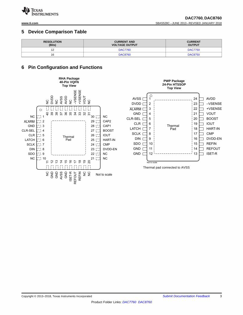
40
NC
11
NC
1NC 30 NC
39
DV
DD
12
GN
D
2ALARM 29 CAP2
38
NC
13
GN
D
3GND 28 CAP1
37
AV
SS
14
AV
SS
4CLR-SEL 27 BOOST
36
AV
DD
15
GN
D
5CLR 26 IOUT
35
NC
16
ISE
T-R
6LATCH 25 HART-IN
34
–V
SE
NS
E17
RE
FO
UT
7SCLK 24 CMP
33
+V
SE
NS
E18
RE
FIN
8DIN 23 DVDD-EN
32
VO
UT
19
NC
9SDO 22 NC
31
NC
20
NC
10NC 21 NC
Not to scale
Thermal
Pad
1AVSS 24 AVDD
2DVDD 23 –VSENSE
3ALARM 22 +VSENSE
4GND 21 VOUT
5CLR-SEL 20 BOOST
6CLR 19 IOUT
7LATCH 18 HART-IN
8SCLK 17 CMP
9DIN 16 DVDD-EN
10SDO 15 REFIN
11GND 14 REFOUT
12GND 13 ISET-R
3
DAC7760, DAC8760www.ti.com SBAS528C –JUNE 2013–REVISED JANUARY 2018
Product Folder Links: DAC7760 DAC8760
Submit Documentation FeedbackCopyright © 2013–2018, Texas Instruments Incorporated
5 Device Comparison Table
RESOLUTION(Bits)
CURRENT ANDVOLTAGE OUTPUT
CURRENTOUTPUT
12 DAC7760 DAC7750
16 DAC8760 DAC8750
6 Pin Configuration and Functions
RHA Package40-Pin VQFN
Top ViewPWP Package
24-Pin HTSSOPTop View
Thermal pad connected to AVSS
4
DAC7760, DAC8760SBAS528C –JUNE 2013–REVISED JANUARY 2018 www.ti.com
Product Folder Links: DAC7760 DAC8760
Submit Documentation Feedback Copyright © 2013–2018, Texas Instruments Incorporated
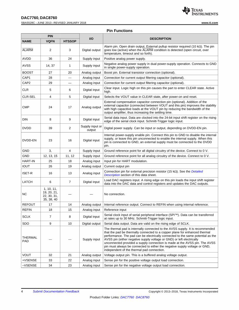
Pin FunctionsPIN
I/O DESCRIPTIONNAME VQFN HTSSOP
ALARM 2 3 Digital outputAlarm pin. Open drain output. External pullup resistor required (10 kΩ). The pingoes low (active) when the ALARM condition is detected (open circuit, overtemperature, timeout and so forth).
AVDD 36 24 Supply input Positive analog power supply.
AVSS 14, 37 1 Supply input Negative analog power supply in dual power-supply operation. Connects to GNDin single power-supply operation.
BOOST 27 20 Analog output Boost pin. External transistor connection (optional).CAP1 28 — Analog input Connection for current output filtering capacitor (optional).CAP2 29 — Analog input Connection for current output filtering capacitor (optional).
CLR 5 6 Digital input Clear input. Logic high on this pin causes the part to enter CLEAR state. Activehigh.
CLR-SEL 4 5 Digital input Selects the VOUT value in CLEAR state, after power-on and reset.
CMP 24 17 Analog output
External compensation capacitor connection pin (optional). Addition of theexternal capacitor (connected between VOUT and this pin) improves the stabilitywith high capacitive loads at the VOUT pin by reducing the bandwidth of theoutput amplifier, thus increasing the settling time.
DIN 8 9 Digital input Serial data input. Data are clocked into the 24-bit input shift register on the risingedge of the serial clock input. Schmitt-Trigger logic input.
DVDD 39 2 Supply input oroutput Digital power supply. Can be input or output, depending on DVDD-EN pin.
DVDD-EN 23 16 Digital input
Internal power-supply enable pin. Connect this pin to GND to disable the internalsupply, or leave this pin unconnected to enable the internal supply. When thispin is connected to GND, an external supply must be connected to the DVDDpin.
GND 3, 4 Supply input Ground reference point for all digital circuitry of the device. Connect to 0 V.GND 12, 13, 15 11, 12 Supply input Ground reference point for all analog circuitry of the device. Connect to 0 V.HART-IN 25 18 Analog input Input pin for HART modulation.IOUT 26 19 Analog output Current output pin
ISET-R 16 13 Analog input Connection pin for external precision resistor (15 kΩ). See the DetailedDescription section of this data sheet.
LATCH 6 7 Digital input Load DAC registers input. A rising edge on this pin loads the input shift registerdata into the DAC data and control registers and updates the DAC outputs.
NC
1, 10, 11,19, 20, 21,22, 30, 31,35, 38, 40
— — No connection.
REFOUT 17 14 Analog output Internal reference output. Connect to REFIN when using internal reference.REFIN 18 15 Analog input Reference input
SCLK 7 8 Digital input Serial clock input of serial peripheral interface (SPI™). Data can be transferredat rates up to 30 MHz. Schmitt-Trigger logic input.
SDO 9 10 Digital output Serial data output. Data are valid on the rising edge of SCLK.
THERMALPAD — — Supply input
The thermal pad is internally connected to the AVSS supply. It is recommendedthat the pad be thermally connected to a copper plane for enhanced thermalperformance. The pad can be electrically connected to the same potential as theAVSS pin (either negative supply voltage or GND) or left electricallyunconnected provided a supply connection is made at the AVSS pin. The AVSSpin must always be connected to either the negative supply voltage or GND,independent of the thermal pad connection.
VOUT 32 21 Analog output Voltage output pin. This is a buffered analog voltage output.+VSENSE 33 22 Analog input Sense pin for the positive voltage output load connection.–VSENSE 34 23 Analog input Sense pin for the negative voltage output load connection.
5
DAC7760, DAC8760www.ti.com SBAS528C –JUNE 2013–REVISED JANUARY 2018
Product Folder Links: DAC7760 DAC8760
Submit Documentation FeedbackCopyright © 2013–2018, Texas Instruments Incorporated
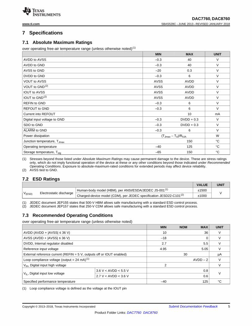
(1) Stresses beyond those listed under Absolute Maximum Ratings may cause permanent damage to the device. These are stress ratingsonly, which do not imply functional operation of the device at these or any other conditions beyond those indicated under RecommendedOperating Conditions. Exposure to absolute-maximum-rated conditions for extended periods may affect device reliability.
(2) AVSS tied to GND.
7 Specifications
7.1 Absolute Maximum Ratingsover operating free-air temperature range (unless otherwise noted) (1)
MIN MAX UNITAVDD to AVSS –0.3 40 VAVDD to GND –0.3 40 VAVSS to GND –20 0.3 VDVDD to GND –0.3 6 VVOUT to AVSS AVSS AVDD VVOUT to GND (2) AVSS AVDD VIOUT to AVSS AVSS AVDD VIOUT to GND (2) AVSS AVDD VREFIN to GND –0.3 6 VREFOUT to GND –0.3 6 VCurrent into REFOUT 10 mADigital input voltage to GND –0.3 DVDD + 0.3 VSDO to GND –0.3 DVDD + 0.3 VALARM to GND –0.3 6 VPower dissipation (TJmax – TA)/RθJA WJunction temperature, TJmax 150 °COperating temperature –40 125 °CStorage temperature, Tstg –65 150 °C
(1) JEDEC document JEP155 states that 500-V HBM allows safe manufacturing with a standard ESD control process.(2) JEDEC document JEP157 states that 250-V CDM allows safe manufacturing with a standard ESD control process.
7.2 ESD RatingsVALUE UNIT
V(ESD) Electrostatic dischargeHuman-body model (HBM), per ANSI/ESDA/JEDEC JS-001 (1) ±1500
VCharged-device model (CDM), per JEDEC specification JESD22-C101 (2) ±1000
(1) Loop compliance voltage is defined as the voltage at the IOUT pin
7.3 Recommended Operating Conditionsover operating free-air temperature range (unless otherwise noted)
MIN NOM MAX UNITAVDD (AVDD + |AVSS| ≤ 36 V) 10 36 VAVSS (AVDD + |AVSS| ≤ 36 V) –18 0 VDVDD, Internal regulator disabled 2.7 5.5 VReference input voltage 4.95 5.05 VExternal reference current (REFIN = 5 V, outputs off or IOUT enabled) 30 µALoop compliance voltage (output = 24 mA) (1) AVDD – 2 VVIH, Digital input high voltage 2 V
VIL, Digital input low voltage3.6 V < AVDD < 5.5 V 0.8
V2.7 V < AVDD < 3.6 V 0.6
Specified performance temperature –40 125 °C
6
DAC7760, DAC8760SBAS528C –JUNE 2013–REVISED JANUARY 2018 www.ti.com
Product Folder Links: DAC7760 DAC8760
Submit Documentation Feedback Copyright © 2013–2018, Texas Instruments Incorporated
(1) For more information about traditional and new thermal metrics, see the Semiconductor and IC Package Thermal Metrics applicationreport.
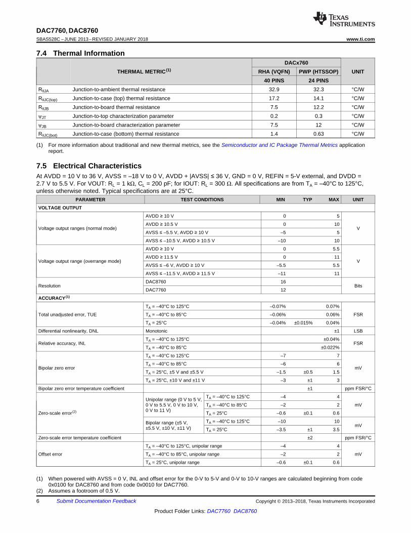
7.4 Thermal Information
THERMAL METRIC (1)DACx760
UNITRHA (VQFN) PWP (HTSSOP)40 PINS 24 PINS
RθJA Junction-to-ambient thermal resistance 32.9 32.3 °C/WRθJC(top) Junction-to-case (top) thermal resistance 17.2 14.1 °C/WRθJB Junction-to-board thermal resistance 7.5 12.2 °C/WψJT Junction-to-top characterization parameter 0.2 0.3 °C/WψJB Junction-to-board characterization parameter 7.5 12 °C/WRθJC(bot) Junction-to-case (bottom) thermal resistance 1.4 0.63 °C/W
(1) When powered with AVSS = 0 V, INL and offset error for the 0-V to 5-V and 0-V to 10-V ranges are calculated beginning from code0x0100 for DAC8760 and from code 0x0010 for DAC7760.
(2) Assumes a footroom of 0.5 V.
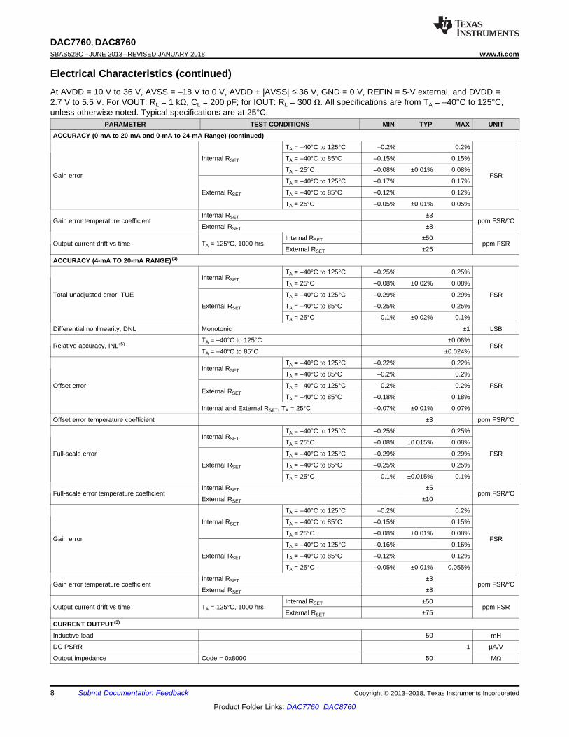
7.5 Electrical CharacteristicsAt AVDD = 10 V to 36 V, AVSS = –18 V to 0 V, AVDD + |AVSS| ≤ 36 V, GND = 0 V, REFIN = 5-V external, and DVDD =2.7 V to 5.5 V. For VOUT: RL = 1 kΩ, CL = 200 pF; for IOUT: RL = 300 Ω. All specifications are from TA = –40°C to 125°C,unless otherwise noted. Typical specifications are at 25°C.
PARAMETER TEST CONDITIONS MIN TYP MAX UNIT
VOLTAGE OUTPUT
Voltage output ranges (normal mode)
AVDD ≥ 10 V 0 5
VAVDD ≥ 10.5 V 0 10
AVSS ≤ –5.5 V, AVDD ≥ 10 V –5 5
AVSS ≤ –10.5 V, AVDD ≥ 10.5 V –10 10
Voltage output range (overrange mode)
AVDD ≥ 10 V 0 5.5
VAVDD ≥ 11.5 V 0 11
AVSS ≤ –6 V, AVDD ≥ 10 V –5.5 5.5
AVSS ≤ –11.5 V, AVDD ≥ 11.5 V –11 11
ResolutionDAC8760 16
BitsDAC7760 12
ACCURACY (1)
Total unadjusted error, TUE
TA = –40°C to 125°C –0.07% 0.07%
FSRTA = –40°C to 85°C –0.06% 0.06%
TA = 25°C –0.04% ±0.015% 0.04%
Differential nonlinearity, DNL Monotonic ±1 LSB
Relative accuracy, INLTA = –40°C to 125°C ±0.04%
FSRTA = –40°C to 85°C ±0.022%
Bipolar zero error
TA = –40°C to 125°C –7 7
mVTA = –40°C to 85°C –6 6
TA = 25°C, ±5 V and ±5.5 V –1.5 ±0.5 1.5
TA = 25°C, ±10 V and ±11 V –3 ±1 3
Bipolar zero error temperature coefficient ±1 ppm FSR/°C
Zero-scale error (2)
Unipolar range (0 V to 5 V,0 V to 5.5 V, 0 V to 10 V,0 V to 11 V)
TA = –40°C to 125°C –4 4
mVTA = –40°C to 85°C –2 2
TA = 25°C –0.6 ±0.1 0.6
Bipolar range (±5 V,±5.5 V, ±10 V, ±11 V)
TA = –40°C to 125°C –10 10mV
TA = 25°C –3.5 ±1 3.5
Zero-scale error temperature coefficient ±2 ppm FSR/°C
Offset error
TA = –40°C to 125°C, unipolar range –4 4
mVTA = –40°C to 85°C, unipolar range –2 2
TA = 25°C, unipolar range –0.6 ±0.1 0.6

7
DAC7760, DAC8760www.ti.com SBAS528C –JUNE 2013–REVISED JANUARY 2018
Product Folder Links: DAC7760 DAC8760
Submit Documentation FeedbackCopyright © 2013–2018, Texas Instruments Incorporated
Electrical Characteristics (continued)At AVDD = 10 V to 36 V, AVSS = –18 V to 0 V, AVDD + |AVSS| ≤ 36 V, GND = 0 V, REFIN = 5-V external, and DVDD =2.7 V to 5.5 V. For VOUT: RL = 1 kΩ, CL = 200 pF; for IOUT: RL = 300 Ω. All specifications are from TA = –40°C to 125°C,unless otherwise noted. Typical specifications are at 25°C.
PARAMETER TEST CONDITIONS MIN TYP MAX UNIT
(3) Specified by design and characterization; not production tested.(4) DAC8760 and DAC7760 current output range is set by writing to RANGE bits in control register at address 0x55.(5) For 0-mA to 20-mA and 0-mA to 24-mA ranges, INL is calculated beginning from code 0x0100 for DAC8760 and from code 0x0010 for
DAC7760.
ACCURACY (continued)
Offset error temperature coefficient ±1 ppm FSR/°C
Gain error
TA = –40°C to 125°C –0.07% 0.07%
FSRTA = –40°C to 85°C –0.06% 0.06%
TA = 25°C –0.04% ±0.01% 0.04%
Gain error temperature coefficient ±3 ppm FSR/°C
Full-scale error
TA = –40°C to 125°C –0.07% 0.07%
FSRTA = –40°C to 85°C –0.06% 0.06%
TA = 25°C –0.04% ±0.01% 0.04%
Full-scale error temperature coefficient ±1 ppm FSR/°C
VOLTAGE OUTPUT (UNIPOLAR AND BIPOLAR MODES)
Headroom AVDD with respect to VOUT full scale 0.5 V
Footroom AVSS with respect to VOUT zero scale –0.5 V
Output voltage drift vs time TA = 125°C, 1000 hrs ±15 ppm FSR
Short-circuit current 30 mA
Load For specified performance 1 kΩ
Capacitive load stability (3)
RL = ∞ 20 nF
RL = 1 kΩ 5 nF
RL = 1 kΩ, external compensation capacitor (4 nF)connected 1 µF
DC output impedance Code = 0x8000 0.3 Ω
DC PSRR (3) No output load 3 10 µV/V
CURRENT OUTPUT
Output current ranges
0 24
mA0 20
4 20
ResolutionDAC8760 16
BitsDAC7760 12
ACCURACY (0-mA to 20-mA and 0-mA to 24-mA Range) (4)
Total unadjusted error, TUE
TA = –40°C to 125°C –0.2% 0.2%
FSRTA = –40°C to 85°C –0.16% 0.16%
TA = 25°C –0.08% ±0.02% 0.08%
Differential nonlinearity, DNL Monotonic ±1 LSB
Relative accuracy, INL (5) TA = –40°C to 125°C ±0.08%FSR
TA = –40°C to 85°C ±0.024%
Offset error
TA = –40°C to 125°C –0.17% 0.17%
FSRTA = –40°C to 85°C –0.1% 0.1%
TA = 25°C –0.07% ±0.01% 0.07%
Offset error temperature coefficient ±5 ppm FSR/°C
Full-scale error
TA = –40°C to 125°C –0.2% 0.2%
FSRTA = –40°C to 85°C –0.16% 0.16%
TA = 25°C –0.08% ±0.015% 0.08%
Full-scale error temperature coefficientInternal RSET ±5
ppm FSR/°CExternal RSET ±10
8
DAC7760, DAC8760SBAS528C –JUNE 2013–REVISED JANUARY 2018 www.ti.com
Product Folder Links: DAC7760 DAC8760
Submit Documentation Feedback Copyright © 2013–2018, Texas Instruments Incorporated
Electrical Characteristics (continued)At AVDD = 10 V to 36 V, AVSS = –18 V to 0 V, AVDD + |AVSS| ≤ 36 V, GND = 0 V, REFIN = 5-V external, and DVDD =2.7 V to 5.5 V. For VOUT: RL = 1 kΩ, CL = 200 pF; for IOUT: RL = 300 Ω. All specifications are from TA = –40°C to 125°C,unless otherwise noted. Typical specifications are at 25°C.
PARAMETER TEST CONDITIONS MIN TYP MAX UNIT
ACCURACY (0-mA to 20-mA and 0-mA to 24-mA Range) (continued)
Gain error
Internal RSET
TA = –40°C to 125°C –0.2% 0.2%
FSR
TA = –40°C to 85°C –0.15% 0.15%
TA = 25°C –0.08% ±0.01% 0.08%
External RSET
TA = –40°C to 125°C –0.17% 0.17%
TA = –40°C to 85°C –0.12% 0.12%
TA = 25°C –0.05% ±0.01% 0.05%
Gain error temperature coefficientInternal RSET ±3
ppm FSR/°CExternal RSET ±8
Output current drift vs time TA = 125°C, 1000 hrsInternal RSET ±50
ppm FSRExternal RSET ±25
ACCURACY (4-mA TO 20-mA RANGE) (4)
Total unadjusted error, TUE
Internal RSETTA = –40°C to 125°C –0.25% 0.25%
FSR
TA = 25°C –0.08% ±0.02% 0.08%
External RSET
TA = –40°C to 125°C –0.29% 0.29%
TA = –40°C to 85°C –0.25% 0.25%
TA = 25°C –0.1% ±0.02% 0.1%
Differential nonlinearity, DNL Monotonic ±1 LSB
Relative accuracy, INL (5) TA = –40°C to 125°C ±0.08%FSR
TA = –40°C to 85°C ±0.024%
Offset error
Internal RSETTA = –40°C to 125°C –0.22% 0.22%
FSR
TA = –40°C to 85°C –0.2% 0.2%
External RSETTA = –40°C to 125°C –0.2% 0.2%
TA = –40°C to 85°C –0.18% 0.18%
Internal and External RSET, TA = 25°C –0.07% ±0.01% 0.07%
Offset error temperature coefficient ±3 ppm FSR/°C
Full-scale error
Internal RSETTA = –40°C to 125°C –0.25% 0.25%
FSR
TA = 25°C –0.08% ±0.015% 0.08%
External RSET
TA = –40°C to 125°C –0.29% 0.29%
TA = –40°C to 85°C –0.25% 0.25%
TA = 25°C –0.1% ±0.015% 0.1%
Full-scale error temperature coefficientInternal RSET ±5
ppm FSR/°CExternal RSET ±10
Gain error
Internal RSET
TA = –40°C to 125°C –0.2% 0.2%
FSR
TA = –40°C to 85°C –0.15% 0.15%
TA = 25°C –0.08% ±0.01% 0.08%
External RSET
TA = –40°C to 125°C –0.16% 0.16%
TA = –40°C to 85°C –0.12% 0.12%
TA = 25°C –0.05% ±0.01% 0.055%
Gain error temperature coefficientInternal RSET ±3
ppm FSR/°CExternal RSET ±8
Output current drift vs time TA = 125°C, 1000 hrsInternal RSET ±50
ppm FSRExternal RSET ±75
CURRENT OUTPUT (3)
Inductive load 50 mH
DC PSRR 1 µA/V
Output impedance Code = 0x8000 50 MΩ
9
DAC7760, DAC8760www.ti.com SBAS528C –JUNE 2013–REVISED JANUARY 2018
Product Folder Links: DAC7760 DAC8760
Submit Documentation FeedbackCopyright © 2013–2018, Texas Instruments Incorporated
Electrical Characteristics (continued)At AVDD = 10 V to 36 V, AVSS = –18 V to 0 V, AVDD + |AVSS| ≤ 36 V, GND = 0 V, REFIN = 5-V external, and DVDD =2.7 V to 5.5 V. For VOUT: RL = 1 kΩ, CL = 200 pF; for IOUT: RL = 300 Ω. All specifications are from TA = –40°C to 125°C,unless otherwise noted. Typical specifications are at 25°C.
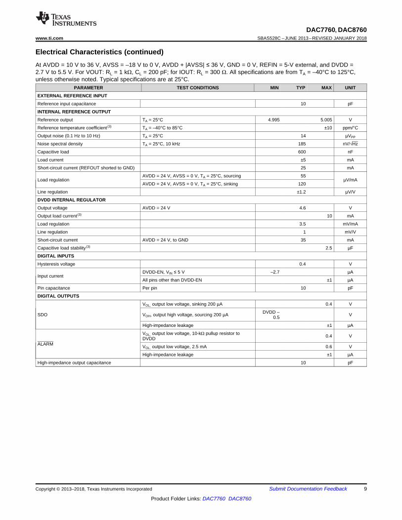
PARAMETER TEST CONDITIONS MIN TYP MAX UNIT
EXTERNAL REFERENCE INPUT
Reference input capacitance 10 pF
INTERNAL REFERENCE OUTPUT
Reference output TA = 25°C 4.995 5.005 V
Reference temperature coefficient (3) TA = –40°C to 85°C ±10 ppm/°C
Output noise (0.1 Hz to 10 Hz) TA = 25°C 14 µVPP
Noise spectral density TA = 25°C, 10 kHz 185 nV/√Hz
Capacitive load 600 nF
Load current ±5 mA
Short-circuit current (REFOUT shorted to GND) 25 mA
Load regulationAVDD = 24 V, AVSS = 0 V, TA = 25°C, sourcing 55
µV/mAAVDD = 24 V, AVSS = 0 V, TA = 25°C, sinking 120
Line regulation ±1.2 µV/V
DVDD INTERNAL REGULATOR
Output voltage AVDD = 24 V 4.6 V
Output load current (3) 10 mA
Load regulation 3.5 mV/mA
Line regulation 1 mV/V
Short-circuit current AVDD = 24 V, to GND 35 mA
Capacitive load stability (3) 2.5 µF
DIGITAL INPUTS
Hysteresis voltage 0.4 V
Input currentDVDD-EN, VIN ≤ 5 V –2.7 µA
All pins other than DVDD-EN ±1 µA
Pin capacitance Per pin 10 pF
DIGITAL OUTPUTS
SDO
VOL, output low voltage, sinking 200 µA 0.4 V
VOH, output high voltage, sourcing 200 µA DVDD –0.5 V
High-impedance leakage ±1 µA
ALARM
VOL, output low voltage, 10-kΩ pullup resistor toDVDD 0.4 V
VOL, output low voltage, 2.5 mA 0.6 V
High-impedance leakage ±1 µA
High-impedance output capacitance 10 pF

10
DAC7760, DAC8760SBAS528C –JUNE 2013–REVISED JANUARY 2018 www.ti.com
Product Folder Links: DAC7760 DAC8760
Submit Documentation Feedback Copyright © 2013–2018, Texas Instruments Incorporated
Electrical Characteristics (continued)At AVDD = 10 V to 36 V, AVSS = –18 V to 0 V, AVDD + |AVSS| ≤ 36 V, GND = 0 V, REFIN = 5-V external, and DVDD =2.7 V to 5.5 V. For VOUT: RL = 1 kΩ, CL = 200 pF; for IOUT: RL = 300 Ω. All specifications are from TA = –40°C to 125°C,unless otherwise noted. Typical specifications are at 25°C.
PARAMETER TEST CONDITIONS MIN TYP MAX UNIT
POWER REQUIREMENTS
AIDD
Outputs disabled, external DVDD 3
mA
Outputs disabled, internal DVDD 4
Code = 0x8000, VOUT enabled, unloaded 4.6
Code = 0x0000, IOUT enabled 3
Code = 0x0000, both outputs enabled, VOUTunloaded 4.6
AISS
Outputs disabled 0.6
mA
Outputs disabled, Internal DVDD 0.6
Code = 0x8000, VOUT enabled, unloaded 2.6
Code = 0x0000, IOUT enabled 0.6
Code = 0x0000, both outputs enabled, VOUTunloaded 2.6
DIDD VIH = DVDD, VIL = GND, interface idle 1 mA
Power dissipation
AVDD = 36 V, AVSS = GND, VOUT enabled,unloaded, DVDD = 5 V 140 170
mWAVDD = 18 V, AVSS = –18 V, VOUT enabled,unloaded, DVDD = 5 V 135
TEMPERATURE
Thermal alarm 142 °C
Thermal alarm hysteresis 18 °C
(1) Specified by characterization, not production tested.
7.6 Electrical Characteristics: ACAt AVDD = 10 V to 36 V, AVSS = –18 V to 0 V, AVDD + |AVSS| ≤ 36 V, GND = 0 V, REFIN = 5-V external; and DVDD = 4.5V to 5.5 V. For VOUT: RL = 2 kΩ, CL = 200 pF; for IOUT: RL = 300 Ω. All specifications –40°C to 125°C, unless otherwisenoted. Typical specifications are at 25°C.
PARAMETER (1) TEST CONDITIONS MIN TYP MAX UNIT
DYNAMIC PERFORMANCE
CURRENT OUTPUT
Output current settling time16-mA step, to 0.1% FSR, no L (inductance) 10
µs16-mA step, to 0.1% FSR, L < 1 mH 25
AC PSRR 200-mV, 50-Hz or 60-Hz sine wavesuperimposed on power-supply voltage –75 dB
VOLTAGE OUTPUT
Output voltage settling time0 V to 10 V, to ±0.03% FSR 22
µs0 V to 5 V, to ±0.03% FSR 13
Slew rate 0.5 V/µs
Power-on glitch energy 2.5 µV-s
Digital-to-analog glitch energy 0.4 µV-s
Glitch impulse peak amplitude 200 mV
Digital feedthrough 2 nV-s
Output noise (0.1-Hz to 10-Hz bandwidth) 0.1 LSBPP
1 / f corner frequency 100 Hz
Output noise spectral density Measured at 10 kHz 180 nV/√Hz
AC PSRR 200-mV, 50-Hz, or 60-Hz sine wavesuperimposed on power-supply voltage –75 dB
11
DAC7760, DAC8760www.ti.com SBAS528C –JUNE 2013–REVISED JANUARY 2018
Product Folder Links: DAC7760 DAC8760
Submit Documentation FeedbackCopyright © 2013–2018, Texas Instruments Incorporated
(1) Specified by design, not production tested.(2) Based on digital interface circuitry only.
When writing to DAC control and config registers, consider the analog output specifications in Electrical Characteristics: AC.
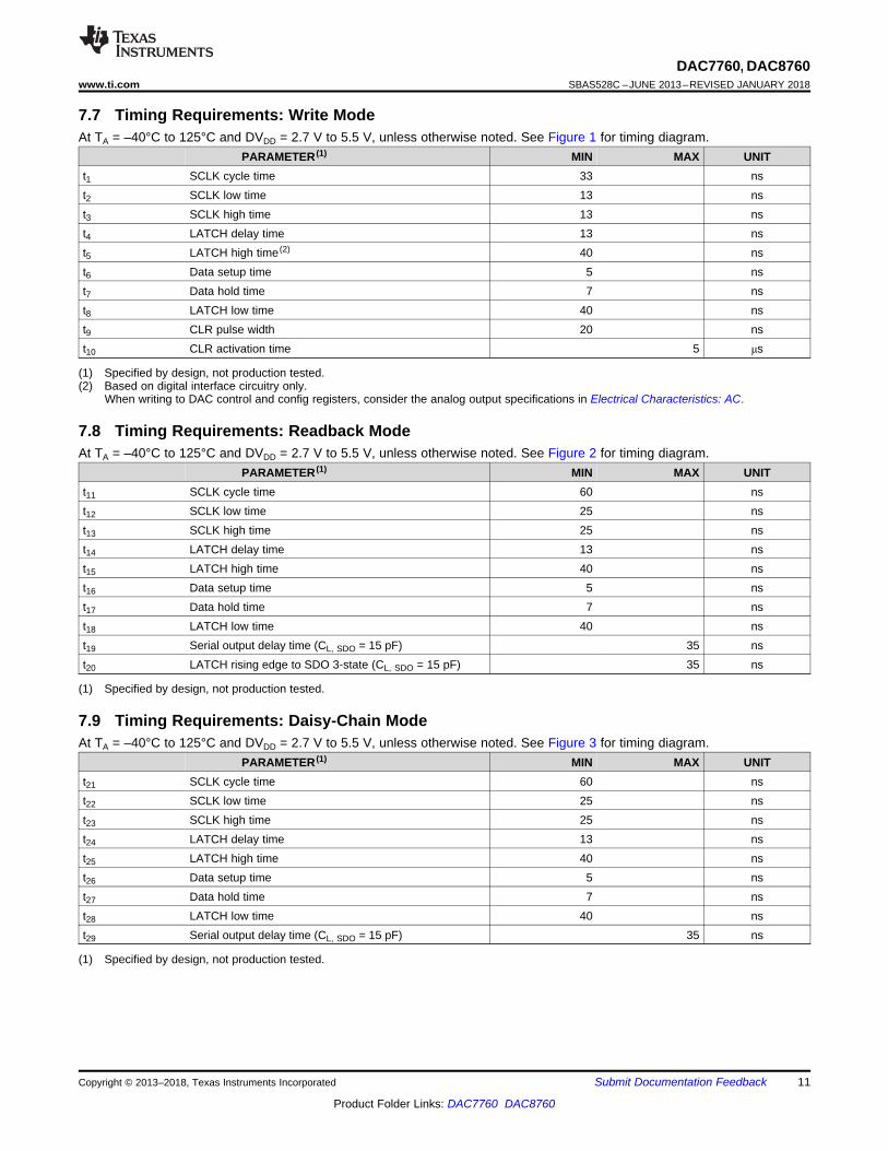
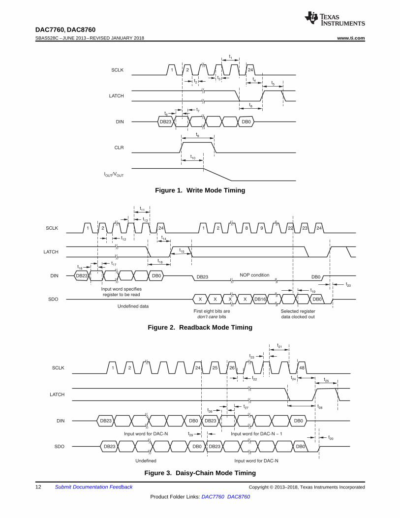
7.7 Timing Requirements: Write ModeAt TA = –40°C to 125°C and DVDD = 2.7 V to 5.5 V, unless otherwise noted. See Figure 1 for timing diagram.
PARAMETER (1) MIN MAX UNITt1 SCLK cycle time 33 nst2 SCLK low time 13 nst3 SCLK high time 13 nst4 LATCH delay time 13 nst5 LATCH high time (2) 40 nst6 Data setup time 5 nst7 Data hold time 7 nst8 LATCH low time 40 nst9 CLR pulse width 20 nst10 CLR activation time 5 μs
(1) Specified by design, not production tested.
7.8 Timing Requirements: Readback ModeAt TA = –40°C to 125°C and DVDD = 2.7 V to 5.5 V, unless otherwise noted. See Figure 2 for timing diagram.
PARAMETER (1) MIN MAX UNITt11 SCLK cycle time 60 nst12 SCLK low time 25 nst13 SCLK high time 25 nst14 LATCH delay time 13 nst15 LATCH high time 40 nst16 Data setup time 5 nst17 Data hold time 7 nst18 LATCH low time 40 nst19 Serial output delay time (CL, SDO = 15 pF) 35 nst20 LATCH rising edge to SDO 3-state (CL, SDO = 15 pF) 35 ns
(1) Specified by design, not production tested.
7.9 Timing Requirements: Daisy-Chain ModeAt TA = –40°C to 125°C and DVDD = 2.7 V to 5.5 V, unless otherwise noted. See Figure 3 for timing diagram.
PARAMETER (1) MIN MAX UNITt21 SCLK cycle time 60 nst22 SCLK low time 25 nst23 SCLK high time 25 nst24 LATCH delay time 13 nst25 LATCH high time 40 nst26 Data setup time 5 nst27 Data hold time 7 nst28 LATCH low time 40 nst29 Serial output delay time (CL, SDO = 15 pF) 35 ns
SCLK
LATCH
DIN
SDO
1 2 24 25 26 48
DB23
DB23 DB23
DB23DB0
DB0 DB0
DB0
t22
t27
t20
t26
t29
t23
t21
t24 t25
t28
Input word for DAC-N 1-Input word for DAC-N
Input word for DAC-NUndefined
SCLK
LATCH
DIN
SDO
1 1 82 2 924 242322
DB23 DB23DB0 DB0
DB0DB16
t12
t17t16
t13
t14
t15
t18
t20
t19
t11
Input word specifies
register to be read
Undefined data
NOP condition
X X X X
First eight bits are
bitsdon’t care
Selected register
data clocked out
SCLK
LATCH
DIN
CLR
I /VOUT OUT
1 2 24
DB23 DB0
t2
t7t6
t3 t4t5
t8
t10
t9
t1
12
DAC7760, DAC8760SBAS528C –JUNE 2013–REVISED JANUARY 2018 www.ti.com
Product Folder Links: DAC7760 DAC8760
Submit Documentation Feedback Copyright © 2013–2018, Texas Instruments Incorporated
Figure 1. Write Mode Timing
Figure 2. Readback Mode Timing
Figure 3. Daisy-Chain Mode Timing
0
100
200
300
400
500
600
700
800
900
1000
10 100 1k 10k 100k
VR
EF
No
ise
PS
D (
nV
/ rt-
Hz)
Frequency (Hz)
C = 700 nF
C = 0 nF
C006
AVDD = 24 V AVSS = 0 V
RE
FO
UT
Noi
se (
2 µV
/div
)
Time (2 s/div)
C001
AVDD = +24 V AVSS = -12 V
4.996
4.997
4.998
4.999
5.000
5.001
5.002
5.003
5.004
-10 -8 -6 -4 -2 0 2 4 6 8 10
RE
FO
UT
(V)
Load Current (mA) C001
AVDD = 24 V AVSS = 0 V
4.995
4.996
4.997
4.998
4.999
5.000
5.001
5.002
5.003
5.004
5.005
10 14 18 22 26 30 34 38
RE
FO
UT
(V)
AVDD (V) C002
TA = 25oC AVSS = 0 V
0
5
10
15
20
25
0.0
1.0
1.0
1.5
2.0
2.5
3.0
3.5
4.0
4.5
5.0
5.5
6.0
6.5
7.0
7.5
8.0
8.5
9.0
9.5
10.0
Po
pu
lati
on
(%
)
Temperature Drift (ppm/oC)
C002
4.995
4.996
4.997
4.998
4.999
5.000
5.001
5.002
5.003
5.004
5.005
-40 -25 -10 5 20 35 50 65 80 95 110 125
Ref
eren
ce O
utp
ut
Vo
ltag
e (V
)
Temperature (oC) C003
30 units shown AVDD = 24 V AVSS = 0 V
13
DAC7760, DAC8760www.ti.com SBAS528C –JUNE 2013–REVISED JANUARY 2018
Product Folder Links: DAC7760 DAC8760
Submit Documentation FeedbackCopyright © 2013–2018, Texas Instruments Incorporated
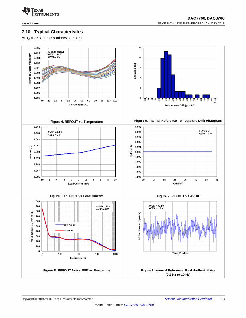
7.10 Typical CharacteristicsAt TA = 25°C, unless otherwise noted.
Figure 4. REFOUT vs Temperature Figure 5. Internal Reference Temperature Drift Histogram
Figure 6. REFOUT vs Load Current Figure 7. REFOUT vs AVDD
Figure 8. REFOUT Noise PSD vs Frequency Figure 9. Internal Reference, Peak-to-Peak Noise(0.1 Hz to 10 Hz)
-1
0
1
2
3
4
5
6
7
8
-40 -35 -30 -25 -20 -15 -10 -5 0 5
Inte
rnal
DV
DD
(V
)
Load Current (mA) C002
TA = 250C Internal DVDD
-90
-80
-70
-60
-50
-40
-30
-20
-10
0
10 100 1k 10k 100k 1M
Inte
rnal
DV
DD
PS
RR
(d
B)
Frequency (Hz) C001
AVDD = 18 V AVSS = -18 V CLOAD = 100 nF
0.0
0.1
0.2
0.3
0.4
0.5
0.6
0.7
0.8
0.9
1.0
2.7 3.1 3.5 3.9 4.3 4.7 5.1 5.5
DID
D (
mA
)
External DVDD (V) C001
TA = 250C External DVDD
0.0
0.5
1.0
1.5
2.0
2.5
3.0
10 13 16 19 22 25 28 31 34 37
AID
D (
mA
)
AVDD (V) C004
External DVDD VOUT disabled IOUT = 0 mA
-3
-2
-1
0
1
2
3
4
5
10 11 12 13 14 15 16 17 18
AID
D/ A
ISS
(m
A)
AVDD/ |AVSS| (V)
AIDD
AISS
C003
AVDD = |AVSS| External DVDD VOUT = 0 V IOUT disabled Output unloaded
Time (200 µs/div)
C002
REFOUT (2 V/div)
AVDD (4 V/div)
AVDD = 10 V AVSS = 0 V
14
DAC7760, DAC8760SBAS528C –JUNE 2013–REVISED JANUARY 2018 www.ti.com
Product Folder Links: DAC7760 DAC8760
Submit Documentation Feedback Copyright © 2013–2018, Texas Instruments Incorporated
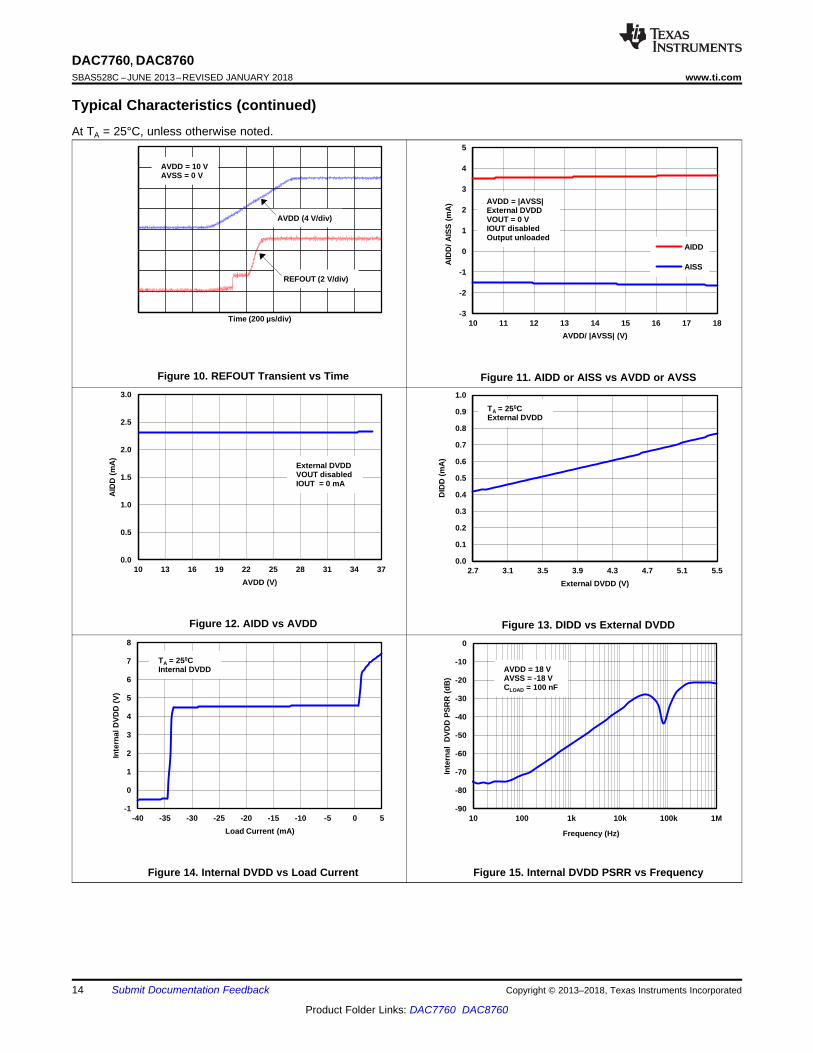
Typical Characteristics (continued)At TA = 25°C, unless otherwise noted.
Figure 10. REFOUT Transient vs Time Figure 11. AIDD or AISS vs AVDD or AVSS
Figure 12. AIDD vs AVDD Figure 13. DIDD vs External DVDD
Figure 14. Internal DVDD vs Load Current Figure 15. Internal DVDD PSRR vs Frequency
-0.010
-0.008
-0.006
-0.004
-0.002
0.000
0.002
0.004
0.006
0.008
0.010
0 8192 16384 24576 32768 40960 49152 57344 65536
INL
Err
or
(%F
SR
)
Code C001
AVDD = +24 V AVSS = 0 V
+5 V/ +10 V range Output unloaded
-0.010
-0.008
-0.006
-0.004
-0.002
0.000
0.002
0.004
0.006
0.008
0.010
0 8192 16384 24576 32768 40960 49152 57344 65536
INL
Err
or
(%F
SR
)
Code C001
AVDD = +24 V AVSS = -12 V
Output unloaded All VOUT ranges
0.000
0.003
0.006
0.009
0.012
0.015
0.018
0.021
0.024
0.027
0.030
-40 -25 -10 5 20 35 50 65 80 95 110 125
To
tal U
nad
just
ed E
rro
r (%
FS
R)
Temperature (0C)
+5 V range
5 V range
+10 V range
10 V range
C002
AVDD = +24 V AVSS = -12 V Output unloaded
-0.04
-0.03
-0.02
-0.01
0.00
0.01
0.02
0.03
0.04
10 11 12 13 14 15 16 17 18
Tot
al U
nadj
uste
d E
rror
(%
FS
R)
AVDD/ |AVSS| (V) C002
Max Total Unadjusted Error
Min Total Unadjusted Error
AVDD = |AVSS| ±10 V range Output unloaded
-0.04
-0.03
-0.02
-0.01
0.00
0.01
0.02
0.03
0.04
0 8192 16384 24576 32768 40960 49152 57344 65536
To
tal U
nad
just
ed E
rro
r (%
FS
R)
Code
+10 V range
+5 V range
C003
AVDD = +24 V AVSS = 0 V Output unloaded
-0.020
-0.015
-0.010
-0.005
0.000
0.005
0.010
0.015
0.020
0 8192 16384 24576 32768 40960 49152 57344 65536
To
tal U
nad
just
ed E
rro
r (%
FS
R)
Code
10 V range 5 V range
+10 V range +5 V range
C003
AVDD = +24 V AVSS = -12 V Output unloaded
15
DAC7760, DAC8760www.ti.com SBAS528C –JUNE 2013–REVISED JANUARY 2018
Product Folder Links: DAC7760 DAC8760
Submit Documentation FeedbackCopyright © 2013–2018, Texas Instruments Incorporated
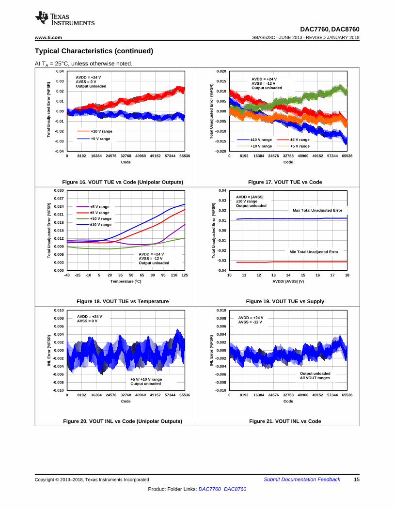
Typical Characteristics (continued)At TA = 25°C, unless otherwise noted.
Figure 16. VOUT TUE vs Code (Unipolar Outputs) Figure 17. VOUT TUE vs Code
Figure 18. VOUT TUE vs Temperature Figure 19. VOUT TUE vs Supply
Figure 20. VOUT INL vs Code (Unipolar Outputs) Figure 21. VOUT INL vs Code

-1.0
-0.8
-0.6
-0.4
-0.2
0.0
0.2
0.4
0.6
0.8
1.0
-40 -25 -10 5 20 35 50 65 80 95 110 125
DN
L E
rro
r (L
SB
)
Temperature (0C) C003
AVDD = +24 V AVSS = -12 V
Max DNL
Min DNL Output unloaded All VOUT ranges
-1.0
-0.8
-0.6
-0.4
-0.2
0.0
0.2
0.4
0.6
0.8
1.0
10 11 12 13 14 15 16 17 18
DN
L E
rror
(LS
B)
AVDD/ |AVSS| (V) C009
Max DNL
Min DNL
±10 V range AVDD = |AVSS| Output unloaded
-1.0
-0.8
-0.6
-0.4
-0.2
0.0
0.2
0.4
0.6
0.8
1.0
0 8192 16384 24576 32768 40960 49152 57344 65536
DN
L E
rro
r (L
SB
)
Code C002
AVDD = 24 V AVSS = 0 V
+5 V/ +10 V range Output unloaded
-1.0
-0.8
-0.6
-0.4
-0.2
0.0
0.2
0.4
0.6
0.8
1.0
0 8192 16384 24576 32768 40960 49152 57344 65536
DN
L E
rro
r (L
SB
)
Code C002
AVDD = +24 V AVSS = -12 V
Output unloaded All VOUT ranges
-0.008
-0.006
-0.004
-0.002
0.000
0.002
0.004
0.006
0.008
0.010
-40 -25 -10 5 20 35 50 65 80 95 110 125
INL
Err
or
(%F
SR
)
Temperature (0C) C002
AVDD = +24 V AVSS = -12 V Max INL
Min INL
Output unloaded All VOUT ranges
-0.010
-0.008
-0.006
-0.004
-0.002
0.000
0.002
0.004
0.006
0.008
0.010
10 11 12 13 14 15 16 17 18
INL
Err
or (
%F
SR
)
AVDD/ |AVSS| (V) C001
Max INL
Min INL
±10 V range AVDD = |AVSS| Output unloaded
16
DAC7760, DAC8760SBAS528C –JUNE 2013–REVISED JANUARY 2018 www.ti.com
Product Folder Links: DAC7760 DAC8760
Submit Documentation Feedback Copyright © 2013–2018, Texas Instruments Incorporated
Typical Characteristics (continued)At TA = 25°C, unless otherwise noted.
Figure 22. VOUT INL vs Temperature Figure 23. VOUT INL vs Supply
Figure 24. VOUT DNL vs Code (Unipolar Outputs) Figure 25. VOUT DNL vs Code
Figure 26. VOUT DNL vs Temperature Figure 27. VOUT DNL vs Supply

-0.8
-0.4
0.0
0.4
0.8
1.2
1.6
2.0
-40 -25 -10 5 20 35 50 65 80 95 110 125
Zer
o S
cale
Err
or
(mV
)
Temperature (0C)
10 V range 5 V range
+10 V range +5 V range
C008
AVDD = +24 V AVSS = -12 V Output unloaded
-0.010
-0.008
-0.006
-0.004
-0.002
0.000
0.002
0.004
0.006
0.008
0.010
-30 -25 -20 -15 -10 -5 0 5 10 15 20 25 30
Cha
nge
in V
OU
TT
(V
)
Source / Sink Current (mA) C010
AVDD = +12 V AVSS = -12 V ±10 V range
-0.020
-0.016
-0.012
-0.008
-0.004
0.000
0.004
0.008
-40 -25 -10 5 20 35 50 65 80 95 110 125
Gai
n E
rro
r (%
FS
R)
Temperature (0C)
10 V range 5 V range
+10 V range +5 V range
AVDD = +24 V AVSS = -12 V Output unloaded
C007
-0.2
0.0
0.2
0.4
0.6
0.8
1.0
-40 -25 -10 5 20 35 50 65 80 95 110 125
Bip
ola
r Z
ero
Err
or
(mV
)
Temperature (0C)
10 V range
5 V range
C006
AVDD = +24 V AVSS = -12 V Output unloaded
-1.0
-0.8
-0.6
-0.4
-0.2
0.0
0.2
0.4
0.6
0.8
1.0
-40 -25 -10 5 20 35 50 65 80 95 110 125
Off
set E
rro
r (m
V)
Temperature (0C)
+10 V range
+5 V range
C005
AVDD = +24 V AVSS = -12 V Output unloaded
-0.012
-0.010
-0.008
-0.006
-0.004
-0.002
0.000
0.002
0.004
-40 -25 -10 5 20 35 50 65 80 95 110 125
Fu
ll S
cale
Err
or
(%F
SR
)
Temperature (0C)
10 V range 5 V range
+10 V range +5 V range
C004
AVDD = +24 V AVSS = -12 V Output unloaded
17
DAC7760, DAC8760www.ti.com SBAS528C –JUNE 2013–REVISED JANUARY 2018
Product Folder Links: DAC7760 DAC8760
Submit Documentation FeedbackCopyright © 2013–2018, Texas Instruments Incorporated
Typical Characteristics (continued)At TA = 25°C, unless otherwise noted.
Figure 28. VOUT Full-Scale Error vs Temperature Figure 29. Offset Error vs Temperature
Figure 30. Bipolar Zero Error vs Temperature Figure 31. Gain Error vs Temperature
Figure 32. Zero-Scale Error vs Temperature Figure 33. VOUT (Full-Scale) vs Load Current(Source or Sink)
20
30
40
50
60
70
0 20 40 60 80 100
Set
tling
Tim
e fo
r 5 V
Ste
p (µ
s)
Load Capacitor (nF) C002
AVDD = +18 V AVSS = -18 V
CMP = 100 pF
0
50
100
150
200
250
0 200 400 600 800 1000
Set
tling
Tim
e fo
r 5 V
Ste
p (µ
s)
Load Capacitor (nF) C003
AVDD = +18 V AVSS = -18 V
CMP = 470 pF
Out
put V
olta
ge (5
V/d
iv)
Time (20 µs/div)
VOUT
LATCH
C001
AVDD = +24 V AVSS = -12 V
From code: FFFFh To code: 0000h
10 V range CLOAD = 200 pF
0
10
20
30
40
50
60
0 5 10 15 20 25
Set
tling
Tim
e fo
r 5 V
Ste
p (µ
s)
Load Capacitor (nF) C001
AVDD = +18 V AVSS = -18 V
CMP = 0 pF
-0.010
-0.008
-0.006
-0.004
-0.002
0.000
0.002
0.004
0.006
0.008
0.010
-25 -20 -15 -10 -5 0 5 10 15 20 25
Cha
nge
in V
OU
TT
(V
)
Source / Sink Current (mA) C009
AVDD = +12 V AVSS = -12 V ±10 V range
Out
put V
olta
ge (5
V/d
iv)
Time (20 µs/div)
VOUT
LATCH
C001
AVDD = +24 V AVSS = -12 V
From code: 0000h To code: FFFFh
10 V range CLOAD = 200 pF
18
DAC7760, DAC8760SBAS528C –JUNE 2013–REVISED JANUARY 2018 www.ti.com
Product Folder Links: DAC7760 DAC8760
Submit Documentation Feedback Copyright © 2013–2018, Texas Instruments Incorporated
Typical Characteristics (continued)At TA = 25°C, unless otherwise noted.
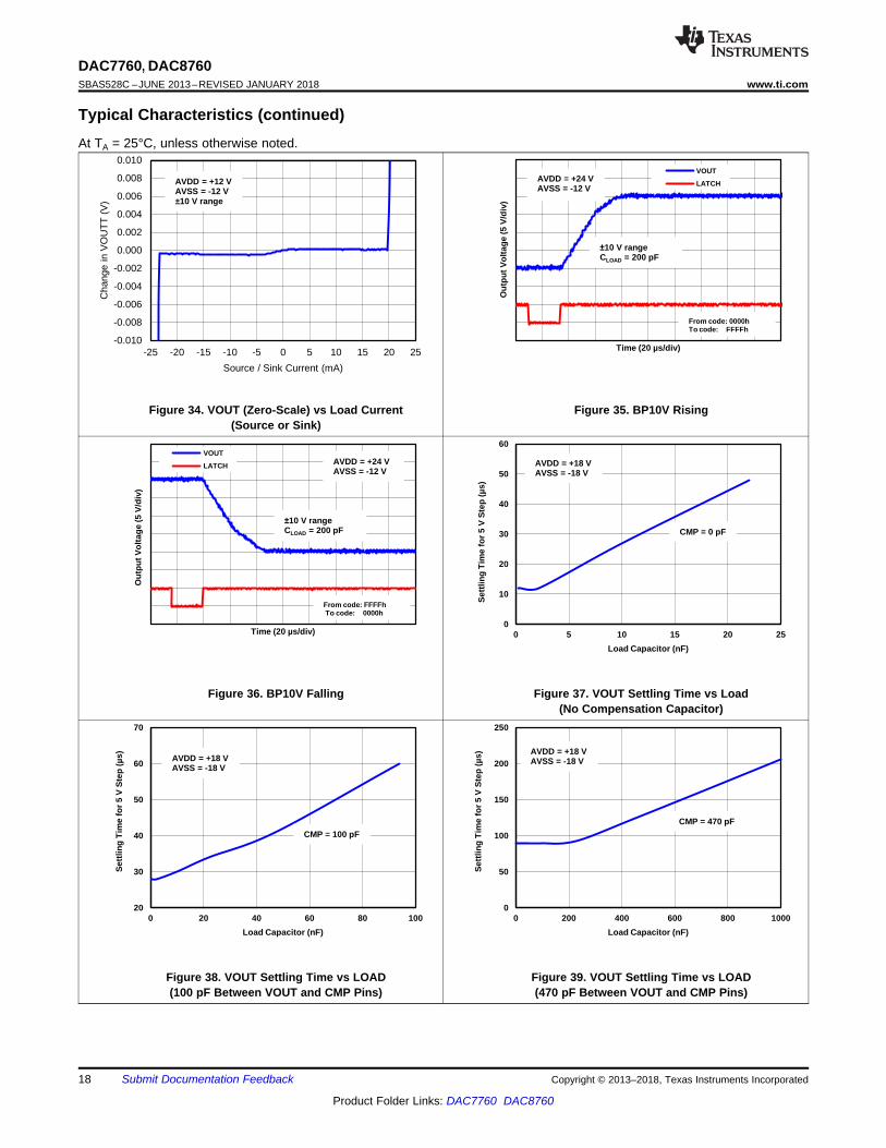
Figure 34. VOUT (Zero-Scale) vs Load Current(Source or Sink)
Figure 35. BP10V Rising
Figure 36. BP10V Falling Figure 37. VOUT Settling Time vs Load(No Compensation Capacitor)
Figure 38. VOUT Settling Time vs LOAD(100 pF Between VOUT and CMP Pins)
Figure 39. VOUT Settling Time vs LOAD(470 pF Between VOUT and CMP Pins)
-0.4
-0.2
0.0
0.2
0.4
0.6
0.8
1.0
1.2
-12 -8 -4 0 4 8 12 16 20 24
Lea
kag
e C
urr
ent
(nA
)
VOUT Pin Voltage (V) C003
AVDD = +24 V AVSS = -12 V Output disabled
0
5
10
15
20
25
30
35
40
45
50
-40 -25 -10 5 20 35 50 65 80 95 110 125
Sh
ort
Cir
cuit
Cu
rren
t (m
A)
Temperature (oC)
VOUT = 0 V, short circuit to AVDD
VOUT = 11 V, short circuit to AVSS
C001
AVDD = 24 V AVSS = -12 V
0
100
200
300
400
500
600
700
800
900
10 100 1k 10k 100k
VO
UT
No
ise
PS
D (
nV
/ rt-
Hz)
Frequency (Hz)
10 V range
+5 V range
5 V range/ +10 V range
C007
AVDD = +24V AVSS = -12V Output unloaded
VO
UT
Noi
se (
1 µV
/div
)
Time (2 s/div)
C002
AVDD = +24 V AVSS = -12 V
DAC = midscale
Time (20 µs/div)
C001
VOUT (50 mV/div)
LOAD = 1 k // 200 pF
VO
UT
(50
mV
/div
)
Time (3 µs/div)
C001
8000h to 7FFFh
7FFFh to 8000h
19
DAC7760, DAC8760www.ti.com SBAS528C –JUNE 2013–REVISED JANUARY 2018
Product Folder Links: DAC7760 DAC8760
Submit Documentation FeedbackCopyright © 2013–2018, Texas Instruments Incorporated
Typical Characteristics (continued)At TA = 25°C, unless otherwise noted.
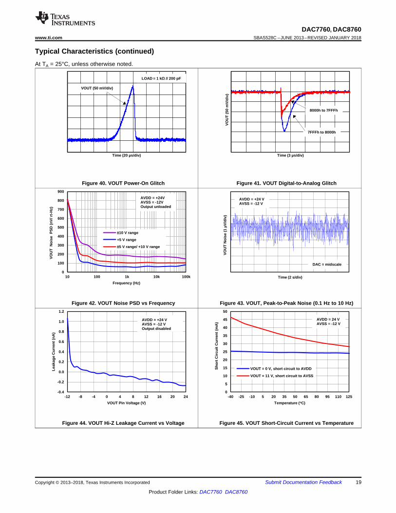
Figure 40. VOUT Power-On Glitch Figure 41. VOUT Digital-to-Analog Glitch
Figure 42. VOUT Noise PSD vs Frequency Figure 43. VOUT, Peak-to-Peak Noise (0.1 Hz to 10 Hz)
Figure 44. VOUT Hi-Z Leakage Current vs Voltage Figure 45. VOUT Short-Circuit Current vs Temperature
0.00
0.01
0.02
0.03
0.04
0.05
0.06
0.07
0.08
-40 -25 -10 5 20 35 50 65 80 95 110 125
To
tal U
nad
just
ed E
rro
r (%
FS
R)
Temperature (oC)
0 mA to 20 mA
0 mA to 24 mA
4 mA to 20 mA
C008
AVDD = 10 V AVSS = 0 V RLOAD = 300
0.00
0.02
0.04
0.06
0.08
0.10
0.12
-40 -25 -10 5 20 35 50 65 80 95 110 125
To
tal U
nad
juat
ed E
rro
r (%
FS
R)
Temperature (oC)
0 mA to 20 mA
0 mA to 24 mA
4 mA to 20 mA
C009
AVDD = 10 V AVSS = 0 V RLOAD = 300
-0.25
-0.20
-0.15
-0.10
-0.05
0.00
0.05
0 8192 16384 24576 32768 40960 49152 57344 65536
To
tal U
nad
just
ed E
rro
r (%
FS
R)
Code
0 mA - 20 mA Internal RSET
0 mA - 20 mA Internal RSET, BOOST
0 mA - 20 mA External RSET
0 mA - 20 mA External RSET, BOOST
C006
AVDD = 24 V AVSS = 0 V RLOAD = 300
-0.25
-0.20
-0.15
-0.10
-0.05
0.00
0.05
0 8192 16384 24576 32768 40960 49152 57344 65536
To
tal U
nad
just
ed E
rro
r (%
FS
R)
Code
4 mA - 20 mA Internal RSET
4 mA - 20 mA Internal RSET, BOOST
4 mA - 20 mA External RSET
4 mA - 20 mA External RSET, BOOST
C003
AVDD = 24 V AVSS = 0 V RLOAD = 300
-90
-80
-70
-60
-50
-40
-30
-20
-10
0
10 100 1k 10k 100k 1M
VO
UT
PS
RR
(d
B)
Frequency (Hz)
+5 V range
10 V range
+10 V Range/ 5 V range
C001
AVDD = +18 V AVSS = -18 V Output unloaded
-0.25
-0.20
-0.15
-0.10
-0.05
0.00
0.05
0 8192 16384 24576 32768 40960 49152 57344 65536
To
tal U
nad
just
ed E
rro
r (%
FS
R)
Code
0 mA - 24 mA Internal RSET
0 mA - 24 mA Internal RSET, BOOST
0 mA - 24 mA External RSET
0 mA - 24 mA External RSET, BOOST
C009
AVDD = 24 V AVSS = 0 V RLOAD = 300
20
DAC7760, DAC8760SBAS528C –JUNE 2013–REVISED JANUARY 2018 www.ti.com
Product Folder Links: DAC7760 DAC8760
Submit Documentation Feedback Copyright © 2013–2018, Texas Instruments Incorporated
Typical Characteristics (continued)At TA = 25°C, unless otherwise noted.
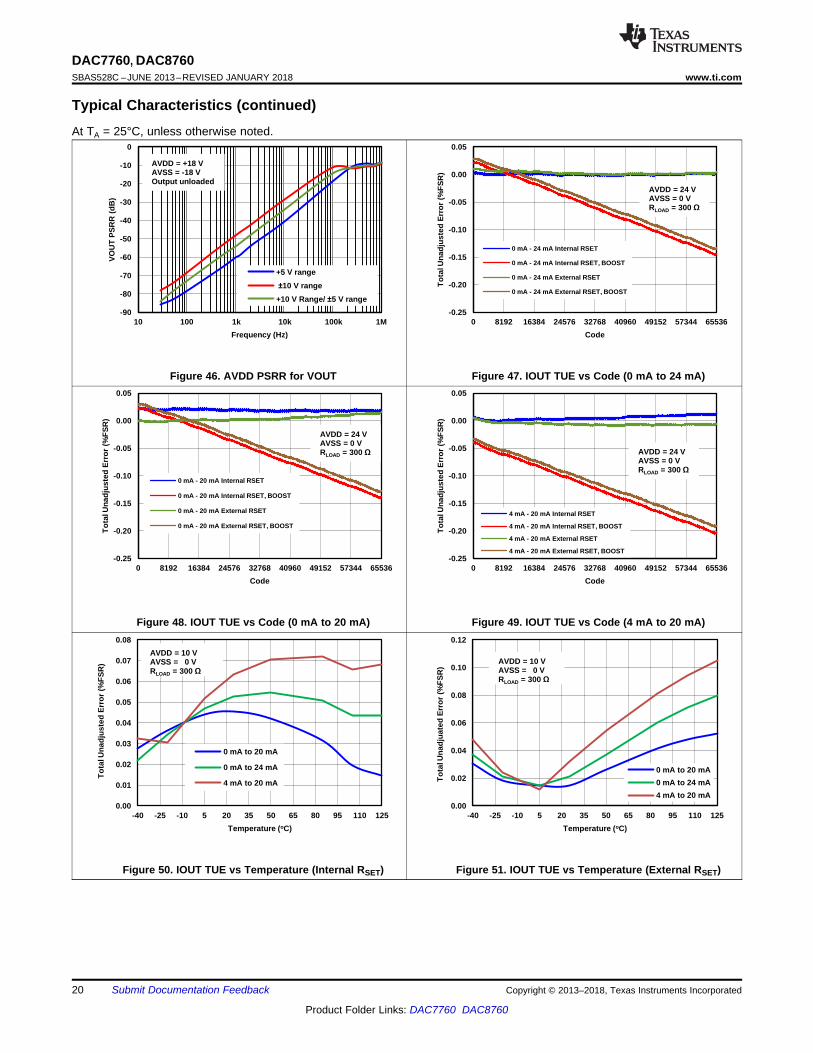
Figure 46. AVDD PSRR for VOUT Figure 47. IOUT TUE vs Code (0 mA to 24 mA)
Figure 48. IOUT TUE vs Code (0 mA to 20 mA) Figure 49. IOUT TUE vs Code (4 mA to 20 mA)
Figure 50. IOUT TUE vs Temperature (Internal RSET) Figure 51. IOUT TUE vs Temperature (External RSET)
-0.008
-0.006
-0.004
-0.002
0.000
0.002
0.004
-40 -25 -10 5 20 35 50 65 80 95 110 125
INL
Err
or
(%F
SR
)
Temperature (oC) C002
Max INL
Min INL
AVDD = 10 V AVSS = 0 V RLOAD = 300 All IOUT ranges
-0.016
-0.012
-0.008
-0.004
0.000
0.004
0.008
0.012
0.016
0 8192 16384 24576 32768 40960 49152 57344 65536
INL
Err
or
(%F
SR
)
Code
4 mA - 20 mA Internal RSET
4 mA - 20 mA Internal RSET, BOOST
4 mA - 20 mA External RSET
4 mA - 20 mA External RSET, BOOST
C001
AVDD = 24 V AVSS = 0 V RLOAD = 300
-0.016
-0.012
-0.008
-0.004
0.000
0.004
0.008
0.012
0.016
0 8192 16384 24576 32768 40960 49152 57344 65536
INL
Err
or
(%F
SR
)
Code
0 mA - 20 mA Internal RSET
0 mA - 20 mA Internal RSET, BOOST
0 mA - 20 mA External RSET
0 mA - 20 mA External RSET, BOOST
C004
AVDD = 24 V AVSS = 0 V RLOAD = 300
-0.016
-0.012
-0.008
-0.004
0.000
0.004
0.008
0.012
0.016
0 8192 16384 24576 32768 40960 49152 57344 65536
INL
Err
or
(%F
SR
)
Code
0 mA - 24 mA Internal RSET
0 mA - 24 mA Internal RSET, BOOST
0 mA - 24 mA External RSET
0 mA - 24 mA External RSET, BOOST
C007
AVDD = 24 V AVSS = 0 V RLOAD = 300
-0.01
0.00
0.01
0.02
0.03
0.04
0.05
10 14 18 22 26 30 34 38
To
tal U
nad
just
ed E
rro
r (%
FS
R)
AVDD (V) C006
Min Total Unadjusted Error
Max Total Unadjusted Error AVSS = 0 V RLOAD = 300 0 mA to 24 mA range
0
0.01
0.02
0.03
0.04
0.05
10 14 18 22 26 30 34 38
To
tal U
nad
just
ed E
rro
r (%
FS
R)
AVDD (V) C005
Max Total Unadjusted Error
Min Total Unadjusted Error
AVSS = 0 V RLOAD = 300 0 mA to 24 mA range
21
DAC7760, DAC8760www.ti.com SBAS528C –JUNE 2013–REVISED JANUARY 2018
Product Folder Links: DAC7760 DAC8760
Submit Documentation FeedbackCopyright © 2013–2018, Texas Instruments Incorporated
Typical Characteristics (continued)At TA = 25°C, unless otherwise noted.
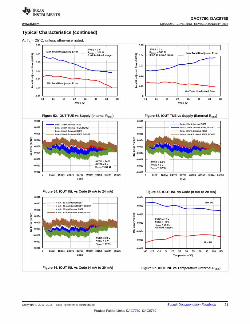
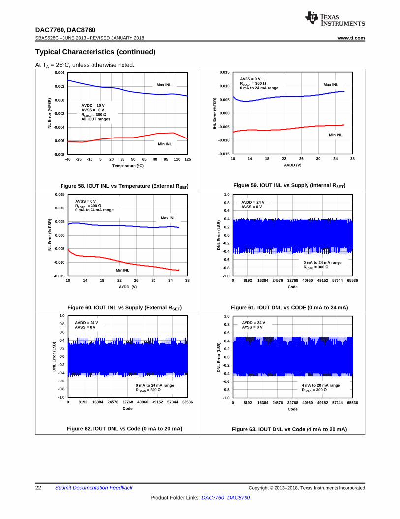
Figure 52. IOUT TUE vs Supply (Internal RSET) Figure 53. IOUT TUE vs Supply (External RSET)
Figure 54. IOUT INL vs Code (0 mA to 24 mA) Figure 55. IOUT INL vs Code (0 mA to 20 mA)
Figure 56. IOUT INL vs Code (4 mA to 20 mA) Figure 57. IOUT INL vs Temperature (Internal RSET)
-1.0
-0.8
-0.6
-0.4
-0.2
0.0
0.2
0.4
0.6
0.8
1.0
0 8192 16384 24576 32768 40960 49152 57344 65536
DN
L E
rro
r (L
SB
)
Code C002
AVDD = 24 V AVSS = 0 V
4 mA to 20 mA range RLOAD = 300
-1.0
-0.8
-0.6
-0.4
-0.2
0.0
0.2
0.4
0.6
0.8
1.0
0 8192 16384 24576 32768 40960 49152 57344 65536
DN
L E
rro
r (L
SB
)
Code C005
AVDD = 24 V AVSS = 0 V
0 mA to 20 mA range RLOAD = 300
-0.015
-0.010
-0.005
0.000
0.005
0.010
0.015
10 14 18 22 26 30 34 38
INL
Err
or
(% F
SR
)
AVDD (V) C003
Max INL
Min INL
AVSS = 0 V RLOAD = 300 0 mA to 24 mA range
-1.0
-0.8
-0.6
-0.4
-0.2
0.0
0.2
0.4
0.6
0.8
1.0
0 8192 16384 24576 32768 40960 49152 57344 65536
DN
L E
rro
r (L
SB
)
Code C008
AVDD = 24 V AVSS = 0 V
0 mA to 24 mA range RLOAD = 300
-0.008
-0.006
-0.004
-0.002
0.000
0.002
0.004
-40 -25 -10 5 20 35 50 65 80 95 110 125
INL
Err
or
(%F
SR
)
Temperature (oC) C001
AVDD = 10 V AVSS = 0 V RLOAD = 300 All IOUT ranges
Max INL
Min INL
-0.015
-0.010
-0.005
0.000
0.005
0.010
0.015
10 14 18 22 26 30 34 38
INL
Err
or
(%F
SR
)
AVDD (V) C004
AVSS = 0 V RLOAD = 300 0 mA to 24 mA range
Max INL
Min INL
22
DAC7760, DAC8760SBAS528C –JUNE 2013–REVISED JANUARY 2018 www.ti.com
Product Folder Links: DAC7760 DAC8760
Submit Documentation Feedback Copyright © 2013–2018, Texas Instruments Incorporated
Typical Characteristics (continued)At TA = 25°C, unless otherwise noted.
Figure 58. IOUT INL vs Temperature (External RSET) Figure 59. IOUT INL vs Supply (Internal RSET)
Figure 60. IOUT INL vs Supply (External RSET) Figure 61. IOUT DNL vs CODE (0 mA to 24 mA)
Figure 62. IOUT DNL vs Code (0 mA to 20 mA) Figure 63. IOUT DNL vs Code (4 mA to 20 mA)

-0.18
-0.12
-0.06
0.00
0.06
0.12
0.18
-40 -25 -10 5 20 35 50 65 80 95 110 125
Fu
ll S
cale
Err
or
(%F
SR
)
Temperature (oC)
0 mA to 20 mA Internal RSET
0 mA to 24 mA Internal RSET
4 mA to 20 mA Internal RSET
0 mA to 20 mA External RSET
0 mA to 24 mA External RSET
4 mA to 20 mA External RSET
C006
AVDD = 10 V AVSS = 0 V RLOAD = 300
-0.12
-0.09
-0.06
-0.03
0.00
0.03
0.06
0.09
0.12
-40 -25 -10 5 20 35 50 65 80 95 110 125
Off
set
Err
or
(%F
SR
)
Temperature (oC)
0 mA to 20 mA Internal RSET 0 mA to 24 mA Internal RSET 4 mA to 20 mA Internal RSET
0 mA to 20 mA External RSET 0 mA to 24 mA External RSET 4 mA to 20 mA External RSET
C003
AVDD = 10 V AVSS = 0 V RLOAD = 300
-1.0
-0.8
-0.6
-0.4
-0.2
0.0
0.2
0.4
0.6
0.8
1.0
10 14 18 22 26 30 34 38
DN
L E
rro
r (L
SB
)
AVDD (V) C008
Max DNL
Min DNL
AVSS = 0 V RLOAD = 300 0 mA to 24 mA range
-1.0
-0.8
-0.6
-0.4
-0.2
0.0
0.2
0.4
0.6
0.8
1.0
10 14 18 22 26 30 34 38
DN
L E
rro
r (L
SB
)
AVDD (V) C007
Max DNL
Min DNL
AVSS = 0 V RLOAD = 300 0 mA to 24 mA range
-1.0
-0.8
-0.6
-0.4
-0.2
0.0
0.2
0.4
0.6
0.8
1.0
-40 -25 -10 5 20 35 50 65 80 95 110 125
DN
L E
rro
r (L
SB
)
Temperature (oC) C010
AVDD = 10 V AVSS = 0 V RLOAD = 300 All IOUT ranges
Max DNL
Min DNL
-1.0
-0.8
-0.6
-0.4
-0.2
0.0
0.2
0.4
0.6
0.8
1.0
-40 -25 -10 5 20 35 50 65 80 95 110 125
DN
L E
rro
r (L
SB
)
Temperature (oC) C011
Max DNL AVDD = 10 V AVSS = 0 V RLOAD = 300 All IOUT ranges
Min DNL
23
DAC7760, DAC8760www.ti.com SBAS528C –JUNE 2013–REVISED JANUARY 2018
Product Folder Links: DAC7760 DAC8760
Submit Documentation FeedbackCopyright © 2013–2018, Texas Instruments Incorporated
Typical Characteristics (continued)At TA = 25°C, unless otherwise noted.
Figure 64. IOUT DNL vs Temperature (Internal RSET) Figure 65. IOUT DNL vs Temperature (External RSET)
Figure 66. IOUT DNL vs Supply (Internal RSET) Figure 67. IOUT DNL vs Supply (External RSET)
Figure 68. IOUT Full-Scale Error vs Temperature Figure 69. IOUT Offset Error vs Temperature
Time (5 µs/div)
IOUT (4 mA/div)
LATCH (5 V/div)
C001
AVDD = +24 V AVSS = 0 V
From code:FFFFh To code: 0000h
4 mA to 20 mA range RLOAD = 300
IOU
T (2
µA
/div
)
Time (60 µs/div)
C001
AVDD = 24 V AVSS = 0 V RLOAD = 300
0
5
10
15
20
25
30
0 1 2 3 4 5 6
IOU
T (m
A)
Headroom Voltage (V) C005
AVDD = 36 V AVSS = 0 V RLOAD = 300
DAC configured to deliver 24 mA
Time (5 µs/div)
IOUT (4 mA/div)
LATCH (5 V/div)
C001
4 mA to 20 mA range RLOAD = 300
From code: 0000h To code: FFFFh
AVDD = +24 V AVSS = 0 V
-0.12
-0.09
-0.06
-0.03
0.00
0.03
0.06
0.09
0.12
-40 -25 -10 5 20 35 50 65 80 95 110 125
Gai
n E
rro
r (%
FS
R)
Temperature (oC)
0 mA to 20 mA Internal RSET 0 mA to 24 mA Internal RSET 4 mA to 20 mA Internal RSET 0 mA to 20 mA External RSET 0 mA to 24 mA External RSET 4 mA to 20 mA External RSET
C007
AVDD = 10 V AVSS = 0 V RLOAD = 300
0.00
0.25
0.50
0.75
1.00
1.25
1.50
1.75
2.00
-40 -25 -10 5 20 35 50 65 80 95 110 125
Co
mp
lian
ce H
ead
roo
m V
olt
age
(V)
Temperature (oC) C004
AVDD = 36 V AVSS = 0 V IOUT = 24 mA RLOAD = 300
24
DAC7760, DAC8760SBAS528C –JUNE 2013–REVISED JANUARY 2018 www.ti.com
Product Folder Links: DAC7760 DAC8760
Submit Documentation Feedback Copyright © 2013–2018, Texas Instruments Incorporated
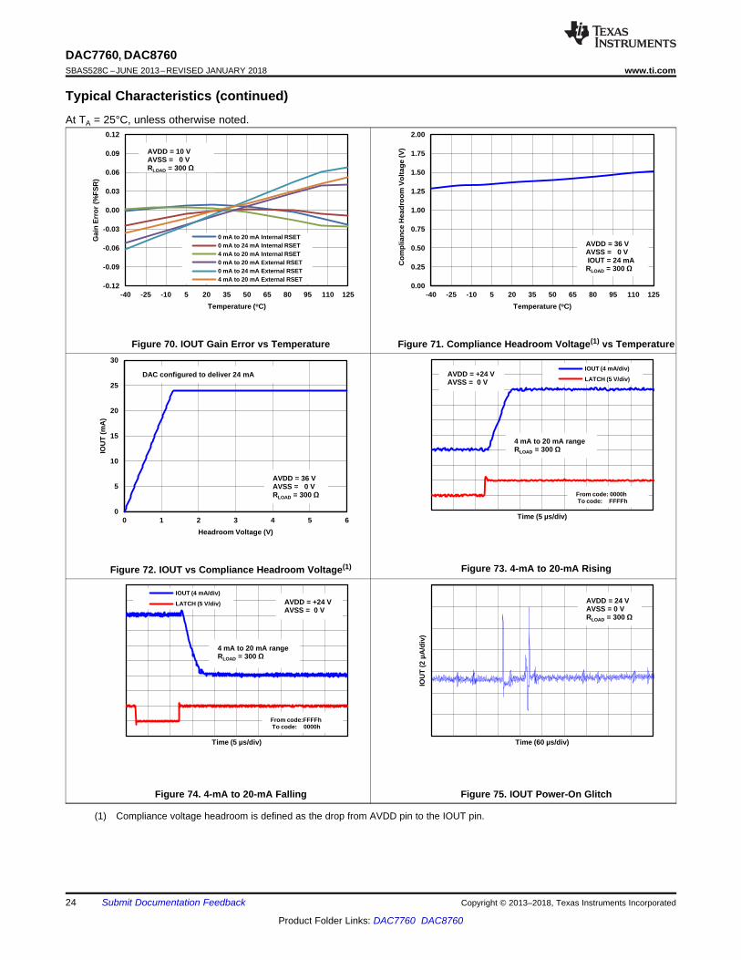
Typical Characteristics (continued)At TA = 25°C, unless otherwise noted.
Figure 70. IOUT Gain Error vs Temperature Figure 71. Compliance Headroom Voltage(1) vs Temperature
Figure 72. IOUT vs Compliance Headroom Voltage(1) Figure 73. 4-mA to 20-mA Rising
Figure 74. 4-mA to 20-mA Falling Figure 75. IOUT Power-On Glitch
(1) Compliance voltage headroom is defined as the drop from AVDD pin to the IOUT pin.
-0.5
0.0
0.5
1.0
1.5
2.0
2.5
3.0
3.5
0 4 8 12 16 20 24 28 32 36
Lea
kag
e C
urr
ent
(nA
)
IOUT Pin Voltage (V) C001
AVDD = 36 V AVSS = 0 V Output disabled
-90
-80
-70
-60
-50
-40
-30
-20
-10
0
10 100 1k 10k 100k 1M
IOU
T P
SR
R (
dB
)
Frequency (Hz) C002
AVDD = 24 V AVSS = 0 V
RLOAD = 250 All IOUT ranges
0
200
400
600
800
1000
1200
10 100 1k 10k 100k
IOU
T N
ois
e P
SD
(n
V/ s
qrt
-Hz)
Frequency (Hz) C003
AVDD = 24 V AVSS = 0 V
RLOAD = 300 All IOUT ranges
IOU
T N
ois
e (2
0 n
A/d
iv)
Time (4 s/div)
C002
0 mA to 20 mA range DAC = midscale
AVDD = 24 V AVSS = 0 V
-0.2
0.0
0.2
0.4
0.6
0.8
1.0
IOU
T (m
A)
Time (2 µs/div)
C002
AVDD = 24 V AVSS = 0 V RLOAD = 300
IOU
T (2
00 µ
A/d
iv)
Time (2 µs/div)
8000h - 7FFFh
7FFFh - 8000h
C001
AVDD = 24 V AVSS = 0 V RLOAD = 250
25
DAC7760, DAC8760www.ti.com SBAS528C –JUNE 2013–REVISED JANUARY 2018
Product Folder Links: DAC7760 DAC8760
Submit Documentation FeedbackCopyright © 2013–2018, Texas Instruments Incorporated
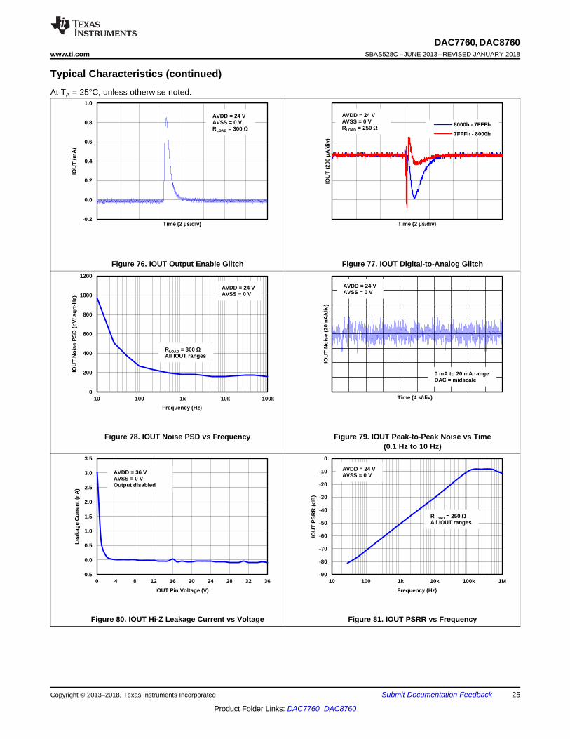
Typical Characteristics (continued)At TA = 25°C, unless otherwise noted.
Figure 76. IOUT Output Enable Glitch Figure 77. IOUT Digital-to-Analog Glitch
Figure 78. IOUT Noise PSD vs Frequency Figure 79. IOUT Peak-to-Peak Noise vs Time(0.1 Hz to 10 Hz)
Figure 80. IOUT Hi-Z Leakage Current vs Voltage Figure 81. IOUT PSRR vs Frequency
DAC
GND
DACx760
AVDDDVDD-EN AVSSDVDD
Pre-Conditioning
CurrentSource
IENABLE ISET-RIGAIN
VGAIN
VENABLE
Current Output Stage
Voltage Output Stage
WatchdogTimer
Slew RateControl
User CalibrationGain/Offset
Register
DAC InputRegister
ThermalAlarm
InternalReference
SP
I S
hift R
egis
ter
Input C
ontr
ol Logic
Contr
ol Logic
CMP
–VSENSE
+VSENSE
VOUT
IOUT
ALARM
BOOST
REFOUT REFIN HART-IN
LATCH
SCLK
DIN
SDO
CLR
CLR-SEL
Copyright © 2016, Texas Instruments Incorporated
26
DAC7760, DAC8760SBAS528C –JUNE 2013–REVISED JANUARY 2018 www.ti.com
Product Folder Links: DAC7760 DAC8760
Submit Documentation Feedback Copyright © 2013–2018, Texas Instruments Incorporated
8 Detailed Description
8.1 OverviewThe DAC8760 and DAC7760 are low-cost, precision, fully-integrated, 16-bit an 12-bit digital-to-analog converters(DACs) designed to meet the requirements of industrial process control applications. These devices can beprogrammed as a current output with a range of 4 mA to 20 mA, 0 mA to 20 mA, or 0 mA to 24 mA; or as avoltage output with a range of 0 V to 5 V, 0 V to 10 V, ±5 V, or ±10 V, with a 10% overrange (0 V to 5.5 V, 0 V to11 V, ±5.5 V, or ±11 V). Both current and voltage outputs can be simultaneously enabled while being controlledby a single data register.
These devices include a power-on-reset function to ensure powering up in a known state (both IOUT and VOUTare disabled and in a high-impedance state). The CLR and CLR-SEL pins set the voltage outputs to zero-scaleor mid-scale, and the current output to the low-end of the range, if the output is enabled. Zero code error andgain error calibration registers can be programmed to digitally calibrate the device in the end system. The outputslew rate is also programmable. These devices can AC couple an external HART signal on the current outputand can operate with either a single 10-V to 36-V supply, or dual supplies up to ±18 V.
8.2 Functional Block Diagram
8.3 Feature Description
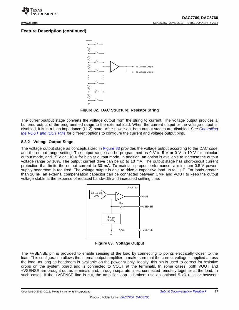
8.3.1 DAC ArchitectureThe DAC8760 and DAC7760 (DACx760) consist of a resistor-string digital-to-analog converter (DAC) followed bya buffer amplifier. The output of the buffer drives the current output and the voltage output. The resistor-stringsection is simply a string of resistors, each of value R, from REF to GND, as Figure 82 illustrates. This type ofarchitecture makes sure the DAC is monotonic. The 16-bit binary digital code (DAC8760) loaded to the DACregister determines at which node on the string the voltage is tapped off before it is fed into the output amplifier.
+12-/16-Bit
DAC
DACx760
í
RangeScaling
RFB
íVSENSE
+VSENSE
VOUT
To Current Output
To Voltage Output
27
DAC7760, DAC8760www.ti.com SBAS528C –JUNE 2013–REVISED JANUARY 2018
Product Folder Links: DAC7760 DAC8760
Submit Documentation FeedbackCopyright © 2013–2018, Texas Instruments Incorporated
Feature Description (continued)
Figure 82. DAC Structure: Resistor String
The current-output stage converts the voltage output from the string to current. The voltage output provides abuffered output of the programmed range to the external load. When the current output or the voltage output isdisabled, it is in a high impedance (Hi-Z) state. After power-on, both output stages are disabled. See Controllingthe VOUT and IOUT Pins for different options to configure the current and voltage output pins.
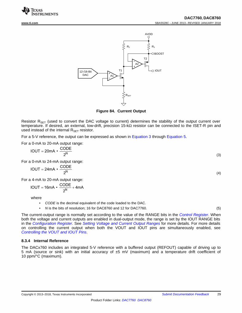
8.3.2 Voltage Output StageThe voltage output stage as conceptualized in Figure 83 provides the voltage output according to the DAC codeand the output range setting. The output range can be programmed as 0 V to 5 V or 0 V to 10 V for unipolaroutput mode, and ±5 V or ±10 V for bipolar output mode. In addition, an option is available to increase the outputvoltage range by 10%. The output current drive can be up to 10 mA. The output stage has short-circuit currentprotection that limits the output current to 30 mA. To maintain proper performance, a minimum 0.5-V power-supply headroom is required. The voltage output is able to drive a capacitive load up to 1 µF. For loads greaterthan 20 nF, an external compensation capacitor can be connected between CMP and VOUT to keep the outputvoltage stable at the expense of reduced bandwidth and increased settling time.
Figure 83. Voltage Output
The +VSENSE pin is provided to enable sensing of the load by connecting to points electrically closer to theload. This configuration allows the internal output amplifier to make sure that the correct voltage is applied acrossthe load, as long as headroom is available on the power supply. Ideally, this pin is used to correct for resistivedrops on the system board and is connected to VOUT at the terminals. In some cases, both VOUT and+VSENSE are brought out as terminals and, through separate lines, connected remotely together at the load. Insuch cases, if the +VSENSE line is cut, the amplifier loop is broken; use an optional 5-kΩ resistor between

N
CODE VREFVOUT VREF • GAIN • GAIN •
22
= -
N
CODEVOUT VREF • GAIN •
2
=
28
DAC7760, DAC8760SBAS528C –JUNE 2013–REVISED JANUARY 2018 www.ti.com
Product Folder Links: DAC7760 DAC8760
Submit Documentation Feedback Copyright © 2013–2018, Texas Instruments Incorporated
Feature Description (continued)VOUT and +VSENSE to prevent this from occurring. The –VSENSE pin, on the other hand, is provided as aGND sense reference output from the internal VOUT amplifier. The output swing of the VOUT amplifier is relativeto the voltage seen at this pin. The actual voltage difference between the –VSENSE pin and the device GNDpins is not expected to be more than a few 100 µV. The internal resistor in Figure 83 between the device internalGND and the –VSENSE pin is typically 2 kΩ.
After power on, the power-on-reset circuit makes sure that all registers are at their default values. Therefore, thevoltage output buffer is in a Hi-Z state; however, the +VSENSE pin connects to the amplifier inputs through aninternal 60-kΩ feedback resistor (RFB in Figure 83). If the VOUT and +VSENSE pins are connected together, theVOUT pin is also connected to the same node through the feedback resistor. This node is protected by internalcircuitry and settles to a value between GND and the reference input.
The output voltage (VOUT) can be expressed as Equation 1 and Equation 2.
For unipolar output mode:
(1)
For bipolar output mode:
where• CODE is the decimal equivalent of the code loaded to the DAC• N is the bits of resolution; 16 for DAC8760 and 12 for DAC7760• VREF is the reference voltage; for internal reference, VREF = 5 V• GAIN is automatically selected for a desired voltage output range as shown in Table 1 (2)
(1) VREF = 5 V
Table 1. Voltage Output Range vs Gain Setting (1)
VOLTAGE OUTPUT GAIN0 V to 5 V 10 V to 10 V 2
±5 V 2±10 V 4
The voltage range is set according to the value of the RANGE bits and the OVR bit in the Control Register. TheOVR bit makes the gain value in Table 1 increase by 10%, thereby increasing the voltage output range, asshown in Table 10 (see Setting Voltage and Current Output Ranges for more details).
8.3.3 Current Output StageThe current output stage consists of a preconditioner and a current source as conceptualized in Figure 84. Thisstage provides a current output according to the DAC code. The output range can be programmed as 0 mA to20 mA, 0 mA to 24 mA, or 4 mA to 20 mA. An external boost transistor can be used to reduce the powerdissipation of the device. The maximum compliance voltage on pin IOUT equals (AVDD – 2 V). In single power-supply mode, the maximum AVDD is 36 V, and the maximum compliance voltage is 34 V. After power on, theIOUT pin is in a Hi-Z state.
N
CODEIOUT 16mA • 4mA
2
= +
N
CODEIOUT 24mA •
2
=
N
CODEIOUT 20mA •
2
=
+12-/16-BitBa_
DACBa_
RSET
R2
T1
A1
+
T2
A2
R3
í
í
IOUT
BOOST
AVDD
29
DAC7760, DAC8760www.ti.com SBAS528C –JUNE 2013–REVISED JANUARY 2018
Product Folder Links: DAC7760 DAC8760
Submit Documentation FeedbackCopyright © 2013–2018, Texas Instruments Incorporated
Figure 84. Current Output
Resistor RSET (used to convert the DAC voltage to current) determines the stability of the output current overtemperature. If desired, an external, low-drift, precision 15-kΩ resistor can be connected to the ISET-R pin andused instead of the internal RSET resistor.
For a 5-V reference, the output can be expressed as shown in Equation 3 through Equation 5.
For a 0-mA to 20-mA output range:
(3)
For a 0-mA to 24-mA output range:
(4)
For a 4-mA to 20-mA output range:
where• CODE is the decimal equivalent of the code loaded to the DAC.• N is the bits of resolution; 16 for DAC8760 and 12 for DAC7760. (5)
The current-output range is normally set according to the value of the RANGE bits in the Control Register. Whenboth the voltage and current outputs are enabled in dual-output mode, the range is set by the IOUT RANGE bitsin the Configuration Register. See Setting Voltage and Current Output Ranges for more details. For more detailson controlling the current output when both the VOUT and IOUT pins are simultaneously enabled, seeControlling the VOUT and IOUT Pins.
8.3.4 Internal ReferenceThe DACx760 includes an integrated 5-V reference with a buffered output (REFOUT) capable of driving up to5 mA (source or sink) with an initial accuracy of ±5 mV (maximum) and a temperature drift coefficient of10 ppm/°C (maximum).

30
DAC7760, DAC8760SBAS528C –JUNE 2013–REVISED JANUARY 2018 www.ti.com
Product Folder Links: DAC7760 DAC8760
Submit Documentation Feedback Copyright © 2013–2018, Texas Instruments Incorporated
8.3.5 Digital Power SupplyAn internally generated 4.6-V supply capable of driving up to 10 mA can be output on DVDD by leaving the DVD-EN pin unconnected. This supply eases the system power supply design especially when an isolation barrier isrequired to cross and generate the digital supply. It can be used to drive isolation components used for the digitaldata lines and other miscellaneous components like references and temp sensors. See Figure 96 for an exampleapplication. If an external supply is preferred, the DVDD pin (which can be driven up to 5.5 V in this case) can bemade into an input by tying DVDD-EN to GND (see Electrical Characteristics for detailed specifications).
8.3.6 DAC ClearThe DAC has an asynchronous clear function through the CLR pin, which is active-high and allows the voltageoutput to be cleared to either zero-scale code or midscale code. This action is user-selectable through the CLR-SEL pin or the CLRSEL bit of Table 19, as Table 2 describes. The CLR-SEL pin and CLRSEL register are ORedtogether. The current output clears to the bottom of its preprogrammed range. When the CLR signal returns tolow, the output remains at the cleared value. The pre-clear value can be restored by pulsing the LATCH signalwithout clocking any data. A new value cannot be programmed until the CLR pin returns to low. Note that in dual-output mode, the value that the DAC data register is cleared to follows the settings for the voltage output mode.
Table 2. CLR-SEL Options
CLR-SELOUTPUT VALUE
UNIPOLAR OUTPUT RANGE BIPOLAR OUTPUT RANGE0 0 V 0 V1 Midscale Negative full-scale
In addition to defining the output value for a clear operation, the CLRSEL bit and the CLR-SEL pin also definethe default output value. During the selection of a new voltage range, the output value corresponds to thedefinitions given in Table 9. To avoid glitches on the output, disable the output by writing a 0 to the OUTEN bit ofthe Table 19 before changing the voltage range. When the OUTEN bit is set to 1, the output goes to the defaultvalue as defined by the CLRSEL bit and the CLR-SEL pin.
8.3.7 Power-Supply SequenceThe DACx760 has internal power on reset (POR) circuitry for both the digital DVDD and analog AVDD supplies.This circuitry makes sure that the internal logic and power-on state of the DAC power up to the proper stateindependent of the supply sequence. The recommended power-supply sequence is to first have the analogAVDD supply come up, followed by the digital supply DVDD. DVDD can also come up first as long as AVDDramps to at least 5 V within 50 µs. If neither of these conditions can be satisfied, TI recommends that a softwarereset command be issued via the SPI bus after both AVDD and DVDD are stable.
8.3.8 Power-On ResetThe DACx760 incorporates two internal POR circuits for the DVDD and AVDD supplies. The DVDD and AVDDPOR signals are ANDed together so that both supplies must be at their minimal specified values for the device tonot be in a reset condition. These POR circuits initialize internal logic and registers as well as set the analogoutputs to a known state while the device supplies are ramping. All registers are reset to their default values withthe default value of the data register being determined by the CLR-SEL pin. The behavior of IOUT and VOUT isdescribed in their respective sections. Typically the POR function can be ignored as long as the device suppliespower up and maintain the specified minimum voltage levels. However, in the case of supply drop or brownout,the DACx760 can have an internal POR reset event or lose digital memory integrity. Figure 85 represents thethreshold levels for the internal POR for both the DVDD and AVDD supplies.

0.00
Supply (V)
Specified SupplyVoltage RangeNo Power-On Reset
Supply Max.
Supply Min.
Power-On Reset
POR Threshold
Undefined
Undefined Operation Threshold
31
DAC7760, DAC8760www.ti.com SBAS528C –JUNE 2013–REVISED JANUARY 2018
Product Folder Links: DAC7760 DAC8760
Submit Documentation FeedbackCopyright © 2013–2018, Texas Instruments Incorporated
Figure 85. Relevant Voltage Levels for POR Circuit
For the DVDD supply, no internal POR occurs for nominal supply operation from 2.7 V (supply minimum) to 5.5 V(supply maximum). For the DVDD supply region between 2.4 V (undefined operation threshold) and 0.8 V (PORthreshold), the internal POR circuit may or may not provide a reset over all temperature conditions. For theDVDD supply below 0.8 V (POR threshold), the internal POR resets as long as the supply voltage is below 0.8 Vfor approximately 1 ms.
For the AVDD supply, no internal POR occurs for nominal supply operation from 10 V (supply minimum) to 36 V(supply maximum). For AVDD supply voltages between 8 V (undefined operation threshold) to 1 V (PORthreshold), the internal POR circuit may or may not provide a reset over all temperature conditions. For theAVDD supply below 1 V (POR threshold), the internal POR resets as long as the supply voltage is below 1 V forapproximately 1 ms. In case the DVDD or AVDD supply drops to a level where the internal POR signal isindeterminate, either power cycle the device or toggle the LATCH pin followed by a software reset. Both optionsinitialize the internal circuitry to a known state and provide proper operation.
8.3.9 Alarm DetectionThe device also provides an alarm detection feature. When one or more of following events occur, the ALARMpin goes low:• The current output load is in open circuit; or• The voltage at IOUT reaches a level where the accuracy of the output current is compromised. This condition
is detected by monitoring internal voltage levels of the IOUT circuitry and is typically below the specifiedcompliance voltage headroom (defined as the voltage drop between the AVDD and IOUT pins) minimum of 2V; or
• The die temperature has exceeded 142°C; or• The SPI watchdog timer exceeded the timeout period (if enabled); or• The SPI frame error CRC check encountered an error (if enabled).
When the ALARM pins of multiple DACx760 devices are connected together to form a wired-AND function, thehost processor must read the status register of each device to know all the fault conditions that are present. Notethat the thermal alarm has hysteresis of about 18°C. After being set, the alarm only resets when the dietemperature drops below 124°C.
8.3.10 Watchdog TimerThis feature is useful to make sure that communication between the host processor and the DACx760 has notbeen lost. It can be enabled by setting the WDEN bit of the Configuration Register to 1. The watchdog timeoutperiod can be set using the WDPD bits of the configuration register; see Table 3. The timer period is based offan internal oscillator with a typical value of 8 MHz.
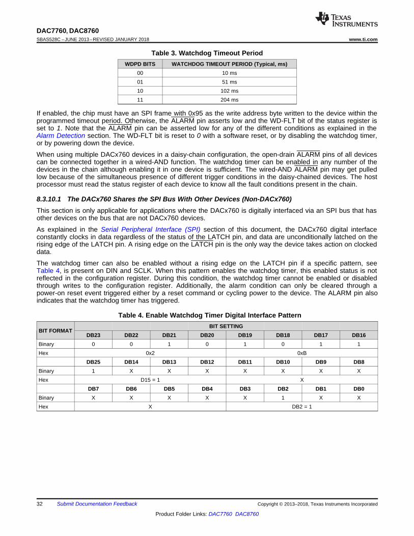
32
DAC7760, DAC8760SBAS528C –JUNE 2013–REVISED JANUARY 2018 www.ti.com
Product Folder Links: DAC7760 DAC8760
Submit Documentation Feedback Copyright © 2013–2018, Texas Instruments Incorporated
Table 3. Watchdog Timeout PeriodWDPD BITS WATCHDOG TIMEOUT PERIOD (Typical, ms)
00 10 ms01 51 ms10 102 ms11 204 ms
If enabled, the chip must have an SPI frame with 0x95 as the write address byte written to the device within theprogrammed timeout period. Otherwise, the ALARM pin asserts low and the WD-FLT bit of the status register isset to 1. Note that the ALARM pin can be asserted low for any of the different conditions as explained in theAlarm Detection section. The WD-FLT bit is reset to 0 with a software reset, or by disabling the watchdog timer,or by powering down the device.
When using multiple DACx760 devices in a daisy-chain configuration, the open-drain ALARM pins of all devicescan be connected together in a wired-AND function. The watchdog timer can be enabled in any number of thedevices in the chain although enabling it in one device is sufficient. The wired-AND ALARM pin may get pulledlow because of the simultaneous presence of different trigger conditions in the daisy-chained devices. The hostprocessor must read the status register of each device to know all the fault conditions present in the chain.
8.3.10.1 The DACx760 Shares the SPI Bus With Other Devices (Non-DACx760)This section is only applicable for applications where the DACx760 is digitally interfaced via an SPI bus that hasother devices on the bus that are not DACx760 devices.
As explained in the Serial Peripheral Interface (SPI) section of this document, the DACx760 digital interfaceconstantly clocks in data regardless of the status of the LATCH pin, and data are unconditionally latched on therising edge of the LATCH pin. A rising edge on the LATCH pin is the only way the device takes action on clockeddata.
The watchdog timer can also be enabled without a rising edge on the LATCH pin if a specific pattern, seeTable 4, is present on DIN and SCLK. When this pattern enables the watchdog timer, this enabled status is notreflected in the configuration register. During this condition, the watchdog timer cannot be enabled or disabledthrough writes to the configuration register. Additionally, the alarm condition can only be cleared through apower-on reset event triggered either by a reset command or cycling power to the device. The ALARM pin alsoindicates that the watchdog timer has triggered.
Table 4. Enable Watchdog Timer Digital Interface Pattern
BIT FORMATBIT SETTING
DB23 DB22 DB21 DB20 DB19 DB18 DB17 DB16Binary 0 0 1 0 1 0 1 1Hex 0x2 0xB
DB25 DB14 DB13 DB12 DB11 DB10 DB9 DB8Binary 1 X X X X X X XHex D15 = 1 X
DB7 DB6 DB5 DB4 DB3 DB2 DB1 DB0Binary X X X X X 1 X XHex X DB2 = 1
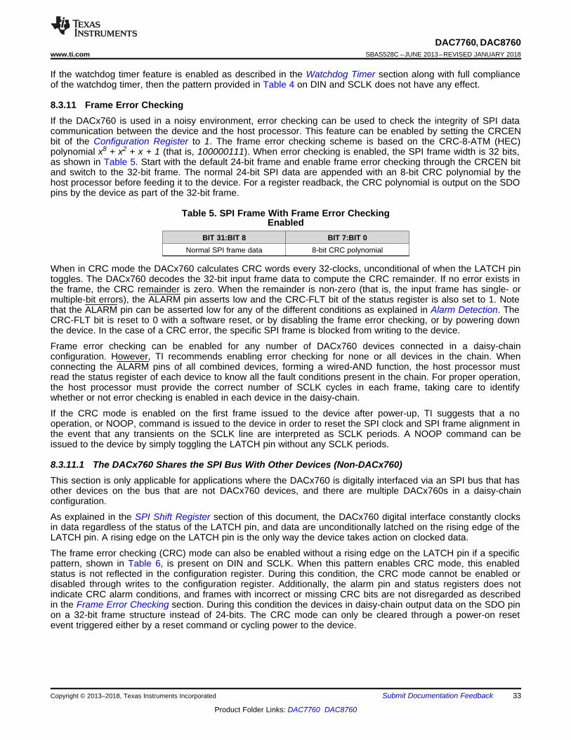
33
DAC7760, DAC8760www.ti.com SBAS528C –JUNE 2013–REVISED JANUARY 2018
Product Folder Links: DAC7760 DAC8760
Submit Documentation FeedbackCopyright © 2013–2018, Texas Instruments Incorporated
If the watchdog timer feature is enabled as described in the Watchdog Timer section along with full complianceof the watchdog timer, then the pattern provided in Table 4 on DIN and SCLK does not have any effect.
8.3.11 Frame Error CheckingIf the DACx760 is used in a noisy environment, error checking can be used to check the integrity of SPI datacommunication between the device and the host processor. This feature can be enabled by setting the CRCENbit of the Configuration Register to 1. The frame error checking scheme is based on the CRC-8-ATM (HEC)polynomial x8 + x2 + x + 1 (that is, 100000111). When error checking is enabled, the SPI frame width is 32 bits,as shown in Table 5. Start with the default 24-bit frame and enable frame error checking through the CRCEN bitand switch to the 32-bit frame. The normal 24-bit SPI data are appended with an 8-bit CRC polynomial by thehost processor before feeding it to the device. For a register readback, the CRC polynomial is output on the SDOpins by the device as part of the 32-bit frame.
Table 5. SPI Frame With Frame Error CheckingEnabled
BIT 31:BIT 8 BIT 7:BIT 0Normal SPI frame data 8-bit CRC polynomial
When in CRC mode the DACx760 calculates CRC words every 32-clocks, unconditional of when the LATCH pintoggles. The DACx760 decodes the 32-bit input frame data to compute the CRC remainder. If no error exists inthe frame, the CRC remainder is zero. When the remainder is non-zero (that is, the input frame has single- ormultiple-bit errors), the ALARM pin asserts low and the CRC-FLT bit of the status register is also set to 1. Notethat the ALARM pin can be asserted low for any of the different conditions as explained in Alarm Detection. TheCRC-FLT bit is reset to 0 with a software reset, or by disabling the frame error checking, or by powering downthe device. In the case of a CRC error, the specific SPI frame is blocked from writing to the device.
Frame error checking can be enabled for any number of DACx760 devices connected in a daisy-chainconfiguration. However, TI recommends enabling error checking for none or all devices in the chain. Whenconnecting the ALARM pins of all combined devices, forming a wired-AND function, the host processor mustread the status register of each device to know all the fault conditions present in the chain. For proper operation,the host processor must provide the correct number of SCLK cycles in each frame, taking care to identifywhether or not error checking is enabled in each device in the daisy-chain.
If the CRC mode is enabled on the first frame issued to the device after power-up, TI suggests that a nooperation, or NOOP, command is issued to the device in order to reset the SPI clock and SPI frame alignment inthe event that any transients on the SCLK line are interpreted as SCLK periods. A NOOP command can beissued to the device by simply toggling the LATCH pin without any SCLK periods.
8.3.11.1 The DACx760 Shares the SPI Bus With Other Devices (Non-DACx760)This section is only applicable for applications where the DACx760 is digitally interfaced via an SPI bus that hasother devices on the bus that are not DACx760 devices, and there are multiple DACx760s in a daisy-chainconfiguration.
As explained in the SPI Shift Register section of this document, the DACx760 digital interface constantly clocksin data regardless of the status of the LATCH pin, and data are unconditionally latched on the rising edge of theLATCH pin. A rising edge on the LATCH pin is the only way the device takes action on clocked data.
The frame error checking (CRC) mode can also be enabled without a rising edge on the LATCH pin if a specificpattern, shown in Table 6, is present on DIN and SCLK. When this pattern enables CRC mode, this enabledstatus is not reflected in the configuration register. During this condition, the CRC mode cannot be enabled ordisabled through writes to the configuration register. Additionally, the alarm pin and status registers does notindicate CRC alarm conditions, and frames with incorrect or missing CRC bits are not disregarded as describedin the Frame Error Checking section. During this condition the devices in daisy-chain output data on the SDO pinon a 32-bit frame structure instead of 24-bits. The CRC mode can only be cleared through a power-on resetevent triggered either by a reset command or cycling power to the device.
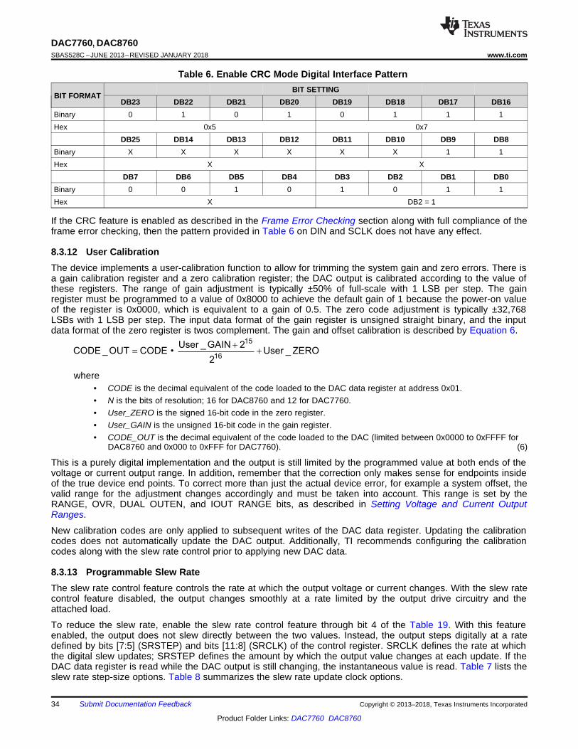
15
16
User _ GAIN 2CODE _ OUT CODE • User _ ZERO
2
+= +
34
DAC7760, DAC8760SBAS528C –JUNE 2013–REVISED JANUARY 2018 www.ti.com
Product Folder Links: DAC7760 DAC8760
Submit Documentation Feedback Copyright © 2013–2018, Texas Instruments Incorporated
Table 6. Enable CRC Mode Digital Interface Pattern
BIT FORMATBIT SETTING
DB23 DB22 DB21 DB20 DB19 DB18 DB17 DB16Binary 0 1 0 1 0 1 1 1Hex 0x5 0x7
DB25 DB14 DB13 DB12 DB11 DB10 DB9 DB8Binary X X X X X X 1 1Hex X X
DB7 DB6 DB5 DB4 DB3 DB2 DB1 DB0Binary 0 0 1 0 1 0 1 1Hex X DB2 = 1
If the CRC feature is enabled as described in the Frame Error Checking section along with full compliance of theframe error checking, then the pattern provided in Table 6 on DIN and SCLK does not have any effect.
8.3.12 User CalibrationThe device implements a user-calibration function to allow for trimming the system gain and zero errors. There isa gain calibration register and a zero calibration register; the DAC output is calibrated according to the value ofthese registers. The range of gain adjustment is typically ±50% of full-scale with 1 LSB per step. The gainregister must be programmed to a value of 0x8000 to achieve the default gain of 1 because the power-on valueof the register is 0x0000, which is equivalent to a gain of 0.5. The zero code adjustment is typically ±32,768LSBs with 1 LSB per step. The input data format of the gain register is unsigned straight binary, and the inputdata format of the zero register is twos complement. The gain and offset calibration is described by Equation 6.
where• CODE is the decimal equivalent of the code loaded to the DAC data register at address 0x01.• N is the bits of resolution; 16 for DAC8760 and 12 for DAC7760.• User_ZERO is the signed 16-bit code in the zero register.• User_GAIN is the unsigned 16-bit code in the gain register.• CODE_OUT is the decimal equivalent of the code loaded to the DAC (limited between 0x0000 to 0xFFFF for
DAC8760 and 0x000 to 0xFFF for DAC7760). (6)
This is a purely digital implementation and the output is still limited by the programmed value at both ends of thevoltage or current output range. In addition, remember that the correction only makes sense for endpoints insideof the true device end points. To correct more than just the actual device error, for example a system offset, thevalid range for the adjustment changes accordingly and must be taken into account. This range is set by theRANGE, OVR, DUAL OUTEN, and IOUT RANGE bits, as described in Setting Voltage and Current OutputRanges.
New calibration codes are only applied to subsequent writes of the DAC data register. Updating the calibrationcodes does not automatically update the DAC output. Additionally, TI recommends configuring the calibrationcodes along with the slew rate control prior to applying new DAC data.
8.3.13 Programmable Slew RateThe slew rate control feature controls the rate at which the output voltage or current changes. With the slew ratecontrol feature disabled, the output changes smoothly at a rate limited by the output drive circuitry and theattached load.
To reduce the slew rate, enable the slew rate control feature through bit 4 of the Table 19. With this featureenabled, the output does not slew directly between the two values. Instead, the output steps digitally at a ratedefined by bits [7:5] (SRSTEP) and bits [11:8] (SRCLK) of the control register. SRCLK defines the rate at whichthe digital slew updates; SRSTEP defines the amount by which the output value changes at each update. If theDAC data register is read while the DAC output is still changing, the instantaneous value is read. Table 7 lists theslew rate step-size options. Table 8 summarizes the slew rate update clock options.

Slew Time =Output Change
Step Size Update Clock Frequency LSB Size· ·
35
DAC7760, DAC8760www.ti.com SBAS528C –JUNE 2013–REVISED JANUARY 2018
Product Folder Links: DAC7760 DAC8760
Submit Documentation FeedbackCopyright © 2013–2018, Texas Instruments Incorporated
Table 7. Slew Rate Step-Size (SRSTEP) Options
SRSTEPSTEP SIZE (LSB)
DAC7760 DAC8760000 0.0625 1001 0.125 2010 0.125 4011 0.5 8100 1 16101 2 32110 4 64111 8 128
Table 8. Slew Rate Update Clock (SRCLK) OptionsSRCLK DAC UPDATE FREQUENCY (Hz)
0000 258,0650001 200,0000010 153,8450011 131,1450100 115,9400101 69,5650110 37,5600111 25,8051000 20,1501001 16,0301010 10,2951011 8,2801100 6,9001101 5,5301110 4,2401111 3,300
The time required for the output to slew over a given range can be expressed as Equation 7:
where• Slew Time is expressed in seconds• Output Change is expressed in amps (A) for IOUT or volts (V) for VOUT (7)
When the slew rate control feature is enabled, all output changes happen at the programmed slew rate. Thisconfiguration results in a staircase formation at the output. If the CLR pin is asserted, the output slews to thezero-scale value at the programmed slew rate. Bit 1 (SR-ON) of the Status Register can be read to verify that theslew operation has completed. The update clock frequency for any given value is the same for all output ranges.The step size, however, varies across output ranges for a given value of step size because the LSB size isdifferent for each output range. Figure 86 illustrates an example of IOUT slewing at a rate set by the previouslydescribed parameters. In this example for the DAC8760 (LSB size of 305 nA for the 0-mA to 20-mA range), thesettings correspond to an update clock frequency of 6.9 kHz and a step size of 128 LSB. As can be seen for thecase with no capacitors on CAP1 or CAP2, the steps occur at the update clock frequency (6.9 kHz correspondsto a period close to 150 µs) and the size of each step is about 38 µA (128 × 305 nA). The slew time for a specificcode change can be calculated using Equation 7.

IOU
T (3
8 µA
/div
) Time (150 µs/ div)
no cap 3 nF CAP1 3 nF CAP2 10 nF CAP1 10 nF CAP2
C001
0 mA to 20 mA range
SRCLK=1100h SRSTEP = 111h
36
DAC7760, DAC8760SBAS528C –JUNE 2013–REVISED JANUARY 2018 www.ti.com
Product Folder Links: DAC7760 DAC8760
Submit Documentation Feedback Copyright © 2013–2018, Texas Instruments Incorporated
Figure 86. IOUT vs Time With Digital Slew Rate Control
Apply the desired programmable slew rate control setting prior to updating the DAC data register becauseupdates to the DAC data register in tandem with updates to the slew rate control registers can create raceconditions that may result in unexpected DAC data.
8.4 Device Functional Modes
8.4.1 Setting Voltage and Current Output RangesFor voltage and current outputs in normal mode (VOUT and IOUT are not simultaneously enabled), the outputrange is set according to Table 9.
(1) RANGE bits cannot be programmed to 0x100. Previous value is held when this command is written.
Table 9. RANGE Bits vs Output RangeRANGE OUTPUT RANGE
000 0 V to +5 V001 0 V to +10 V010 ±5 V011 ±10 V100 Not allowed (1)
101 4 mA to 20 mA110 0 mA to 20 mA111 0 mA to 24 mA
Note that changing the RANGE bits at any time causes the DAC data register to be cleared based on the valueof CLR-SEL (pin or register bit) and the new value of the RANGE bits.
37
DAC7760, DAC8760www.ti.com SBAS528C –JUNE 2013–REVISED JANUARY 2018
Product Folder Links: DAC7760 DAC8760
Submit Documentation FeedbackCopyright © 2013–2018, Texas Instruments Incorporated
In addition to the RANGE bits, the OVR bit extends the voltage output range by 10%. if the OVR bit is set, thevoltage output range follows Table 10, as long as there is headroom with the supply.
Table 10. Voltage Output OverrangeVOLTAGE OUTPUT RANGE VOLTAGE OUTPUT OVERRANGE
0 V to 5 V 0 V to 5.5 V0 V to 10 V 0 V to +11 V
±5 V ±5.5 V±10 V ±11 V
When VOUT and IOUT are simultaneously enabled (dual-output mode) by setting the DUAL OUTEN bit in theConfiguration Register, the voltage output is controlled by the RANGE bits in the Control Register (see Table 11),and the current output is controlled by the IOUT RANGE bits in the Configuration Register (see Table 12).
(1) RANGE bits cannot be programmed to 0x100. Previous value is held when this command is written.
Table 11. RANGE Bits versus Voltage Output Range in Dual-Output ModeRANGE OUTPUT RANGE
000 0 V to +5 V001 0 V to +10 V010 ±5 V011 ±10 V100 Not allowed (1)
1xx Disabled
Table 12. IOUT RANGE Bits vs Current Output Range in Dual-Output ModeRANGE OUTPUT RANGE
00 Disabled01 4 mA to 20 mA10 0 mA to 20 mA11 0 mA to 24 mA
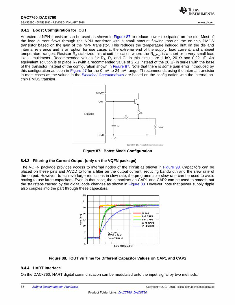
1
4
7
10
13
16
19
22
25
IOU
T (m
A)
Time (200 µs/div)
no cap 3 nF CAP1 3 nF CAP2 10 nF CAP1 10 nF CAP2
C001
TA = 25ºC AVDD = 24 V RLOAD = 250
R1
R2
RLOADC1
DACx760
BOOST
IOUT
GND
Copyright © 2016, Texas Instruments Incorporated
38
DAC7760, DAC8760SBAS528C –JUNE 2013–REVISED JANUARY 2018 www.ti.com
Product Folder Links: DAC7760 DAC8760
Submit Documentation Feedback Copyright © 2013–2018, Texas Instruments Incorporated
8.4.2 Boost Configuration for IOUTAn external NPN transistor can be used as shown in Figure 87 to reduce power dissipation on the die. Most ofthe load current flows through the NPN transistor with a small amount flowing through the on-chip PMOStransistor based on the gain of the NPN transistor. This reduces the temperature induced drift on the die andinternal reference and is an option for use cases at the extreme end of the supply, load current, and ambienttemperature ranges. Resistor R2 stabilizes this circuit for cases where the RLOAD is a short or a very small loadlike a multimeter. Recommended values for R1, R2 and C1 in this circuit are 1 kΩ, 20 Ω and 0.22 µF. Anequivalent solution is to place R2 (with a recommended value of 2 kΩ instead of the 20 Ω) in series with the baseof the transistor instead of the configuration shown in Figure 87. Note that there is some gain error introduced bythis configuration as seen in Figure 47 for the 0-mA to 24-mA range. TI recommends using the internal transistorin most cases as the values in the Electrical Characteristics are based on the configuration with the internal on-chip PMOS transitor.
Figure 87. Boost Mode Configuration
8.4.3 Filtering the Current Output (only on the VQFN package)The VQFN package provides access to internal nodes of the circuit as shown in Figure 93. Capacitors can beplaced on these pins and AVDD to form a filter on the output current, reducing bandwidth and the slew rate ofthe output. However, to achieve large reductions in slew rate, the programmable slew rate can be used to avoidhaving to use large capacitors. Even in that case, the capacitors on CAP1 and CAP2 can be used to smooth outthe stairsteps caused by the digital code changes as shown in Figure 88. However, note that power supply ripplealso couples into the part through these capacitors.
Figure 88. IOUT vs Time for Different Capacitor Values on CAP1 and CAP2
8.4.4 HART InterfaceOn the DACx760, HART digital communication can be modulated onto the input signal by two methods:
Bit
Boundary
Phase
Continuous2200 Hz
(space)
1200 Hz
(mark)
Time
5.5 mA
6.5 mA
6.0 mA
Loop C
urr
ent
Bit Cell Time = 833 sm
39
DAC7760, DAC8760www.ti.com SBAS528C –JUNE 2013–REVISED JANUARY 2018
Product Folder Links: DAC7760 DAC8760
Submit Documentation FeedbackCopyright © 2013–2018, Texas Instruments Incorporated
8.4.4.1 For 4-mA to 20-mA ModeThis method is limited to the case where the RANGE bits of the Table 19 are programmed to the 4-mA to 20-mArange. Some applications require going beyond the 4-mA to 20-mA range. In those cases, see second methoddescribed in this section.
The external HART signal (ac voltage; 500 mVPP, 1200 Hz and 2200 Hz) can be capacitively coupled in throughthe HART-IN pin and transferred to a current that is superimposed on the 4-mA to 20-mA current output. TheHART-IN pin has a typical input impedance of 35 kΩ that together with the input capacitor used to couple theexternal HART signal forms a filter to attenuate frequencies beyond the HART band-pass region. In addition tothis filter, an external passive filter is recommended to complete the filtering requirements of the HARTspecifications. Figure 89 illustrates the output current versus time operation for a typical HART signal.
Note: DC current = 6 mA.
Figure 89. Output Current vs Time
Table 13 specifies the performance of the HART-IN pin.
Table 13. HART-IN Pin CharacteristicsPARAMETER TEST CONDITIONS MIN TYP MAX UNIT
Input impedance HART signal ac-coupled into pin 35 kΩOutput current (peak-to-peak) Input signal of 500 mV (peak-to-peak) 0.9 1 1.1 mA
8.4.4.2 For All Current Output ModesThe use of the HART-IN pin to implement HART modulation is limited to the case where the RANGE bits of theTable 19 are set to the 4-mA to 20-mA range. To implement HART in all current-output modes, seeImplementing HART in All Current Output Modes.
8.5 Programming
8.5.1 Serial Peripheral Interface (SPI)The device is controlled over a versatile four-wire serial interface (SDI, SDO, SCLK, and LATCH) that operates atclock rates of up to 30 MHz and is compatible with SPI, QSPI™, Microwire, and digital signal processing (DSP)standards. The SPI communication command consists of a write address byte and a data word for a total of 24bits. The timing for the digital interface is shown in Figure 1, Figure 2, and Figure 3.
8.5.1.1 SPI Shift RegisterThe default frame is 24 bits wide (refer to the Frame Error Checking section for 32-bit frame mode) and beginswith the rising edge of SCLK that clocks in the MSB. The subsequent bits are latched on successive rising edgesof SCLK. The default 24-bit input frame consists of an 8-bit address byte followed by a 16-bit data word asshown in Table 14.

40
DAC7760, DAC8760SBAS528C –JUNE 2013–REVISED JANUARY 2018 www.ti.com
Product Folder Links: DAC7760 DAC8760
Submit Documentation Feedback Copyright © 2013–2018, Texas Instruments Incorporated
Table 14. Default SPI FrameBIT 23:BIT 16 BIT 15:BIT 0Address byte Data word
The host processor must issue 24 bits before it issues a rising edge on the LATCH pin. Input data bits areclocked in regardless of the LATCH pin and are unconditionally latched on the rising edge of LATCH. By default,the SPI shift register resets to 000000h at power on or after a reset.
8.5.1.2 Write OperationA write operation is accomplished when the address byte is set according to Table 15. For more information onthe DACx760 registers, see DACx760 Commands and Register Map.
Table 15. Write Address FunctionsADDRESS BYTE FUNCTION
0x00 No operation (NOP)0x01 Write DAC Data register0x02 Register read0x55 Write control register0x56 Write reset register0x57 Write configuration register0x58 Write DAC gain calibration register0x59 Write DAC zero calibration register0x95 Watchdog timer reset
8.5.1.3 Read OperationA read operation is accomplished when the address byte is 0x02. Follow the read operation with a no-operation(NOP) command to clock out an addressed register, as shown in Figure 2. To read from a register, the addressbyte and data word is as shown in Table 16. The read register value is output MSB first on SDO on successivefalling edges of SCLK.
Table 16. Default SPI Frame for Register Read
ADDRESS BYTEDATA WORD
BIT 15:BIT 6 BIT 5:BIT 00x02 X (don't care) Register read address (see Table 17)
Table 17 shows the register read addresses available on the DACx760 devices.
(1) X denotes don't care bits.
Table 17. Register Read Address FunctionsREAD ADDRESS (1) FUNCTION
XX XX00 Read status registerXX XX01 Read DAC data registerXX XX10 Read control register00 1011 Read configuration register01 0011 Read DAC gain calibration register01 0111 Read DAC zero calibration register
8.5.1.4 Stand-Alone OperationSCLK can operate in either continuous or burst mode as long as the LATCH rising edge occurs after theappropriate number of SCLK cycles. Providing more than or less than 24 SCLK cycles before the rising edge ofLATCH results in incorrect data being programmed into the device registers and incorrect data sent out on SDO.The rising edge of SCLK that clocks in the MSB of the 24-bit input frame marks the beginning of the write cycle,and data are written to the addressed registers on the rising edge of LATCH.
C B A
SDI
LATCH
SCLK
SDI-B SDI-ASDI-C SDO-C SDO-B SDO-BSDO
41
DAC7760, DAC8760www.ti.com SBAS528C –JUNE 2013–REVISED JANUARY 2018
Product Folder Links: DAC7760 DAC8760
Submit Documentation FeedbackCopyright © 2013–2018, Texas Instruments Incorporated
8.5.1.5 Daisy-Chain OperationFor systems that contain multiple DACx760s, use the SDO pin to daisy-chain several devices. This mode isuseful in reducing the number of serial interface lines in applications that use multiple SPI devices. Daisy-chainmode is enabled by setting the DCEN bit of the control register to 1. By connecting the SDO of the first device tothe SDI input of the next device in the chain, a multiple-device interface is constructed, as Figure 90 illustrates.
Figure 90. Three DACx760s in Daisy-Chain Mode
Like stand-alone operation, the SPI daisy-chain write operation requires one frame, and the read requires twoframes. The rising edge of SCLK that clocks in the MSB of the input frame marks the beginning of the writecycle. When the serial transfer to all devices is complete, LATCH is taken high. This action transfers the datafrom the SPI shift registers to the device internal register of each DACx760 in the daisy-chain. However, thenumber of clocks in each frame in this case depends on the number of devices in the daisy chain. For twodevices, each frame is 48 clocks; the first 24 clocks are for the second DAC and the next 24 bits are for the firstDAC. For a readback, the data are read from the two DACs in the following 48-bit frame; the first 24 clocks arefor the second DAC and the next 24 clocks are for the first DAC. The input data to the DACs during the secondframe can be another command or NOP. Similar to the two-device case described, for N devices, each frame isN × 24 clocks, where N is the total number of DACx760s in the chain.
The serial clock can be a continuous or gated clock. A continuous SCLK source can only be used if LATCH istaken high after the correct number of clock cycles. In gated clock mode, a burst clock containing the exactnumber of clock cycles must be used and LATCH must be taken high after the final clock to latch the data.
42
DAC7760, DAC8760SBAS528C –JUNE 2013–REVISED JANUARY 2018 www.ti.com
Product Folder Links: DAC7760 DAC8760
Submit Documentation Feedback Copyright © 2013–2018, Texas Instruments Incorporated
(1) X denotes don't care bits.(2) DAC8760 (16-bit version) shown. DAC7760 (12-bit version) contents are located in DB15:DB4.
For DAC7760, DB3:DB0 are don't care bits when writing and zeros when reading.(3) No operation, read operation, and watchdog timer are commands and not registers.
8.6 Register Maps
8.6.1 DACx760 Commands and Register MapTable 18 shows the available commands and registers on the DACx760 devices. No operation, read operation,and watchdog timer refer to commands and are not explicit registers. For more information on these commands,see Read Operation and Watchdog Timer. See DACx760 Register Descriptions for descriptions of all DACx760registers.
Table 18. Command and Register MapREGISTER /COMMAND
READ/WRITEACCESS
DATA BITS (DB15:DB0)
15 14 13 12 11 10:9 8 7 6 5 4 3 2 1 0
Control R/W CLRSEL OVR REXT OUTEN SRCLK SRSTEP SREN DCEN RANGE
Configuration R/W X (1) IOUTRANGE
DUALOUTEN APD Reser
ved CALEN HARTEN CRCEN WDEN WDPD
DAC Data (2) R/W D15:D0
No operation (3) — X
Read Operation (3) — X READ ADDRESS
Reset W RESET
Status R Reserved CRC-FLT WD-FLT I-FLT SR-
ON T-FLT
DAC GainCalibration (2) RW G15:G0, unsigned
DAC Zero Calibration(2) RW Z15:Z0, signed
Watchdog Timer (3) — X
8.6.1.1 DACx760 Register Descriptions
8.6.1.1.1 Control Register
The DACx760 control register is written to at address 0x55. Table 19 shows the description for the controlregister bits.
Table 19. Control Register 0x55DATA BIT(S) NAME DEFAULT DESCRIPTION
DB15 CLRSEL 0
VOUT clear value select bit.When bit = 0, VOUT is 0 V in DAC Clear mode or after reset.When bit = 1, VOUT is midscale in unipolar output and negative-full-scale in bipolar outputin DAC Clear mode or after reset.
DB14 OVR 0 Setting the bit increases the voltage output range by 10%.
DB13 REXT 0 External current setting resistor enable.
DB12 OUTEN 0Output enable.Bit = 1: Output is determined by RANGE bits.Bit = 0: Output is disabled. IOUT and VOUT are Hi-Z.
DB11:DB8 SRCLK[3:0] 0000 Slew rate clock control. Ignored when bit SREN = 0
DB7:DB5 SRSTEP[2:0] 000 Slew rate step size control. Ignored when bit SREN = 0
DB4 SREN 0
Slew Rate Enable.Bit = 1: Slew rate control is enabled, and the ramp speed of the output change isdetermined by SRCLK and SRSTEP.Bit = 0: Slew rate control is disabled. Bits SRCLK and SRSTEP are ignored. The outputchanges to the new level immediately.
DB3 DCEN 0 Daisy-chain enable.
DB2:DB0 RANGE[2:0] 000 Output range bits.
43
DAC7760, DAC8760www.ti.com SBAS528C –JUNE 2013–REVISED JANUARY 2018
Product Folder Links: DAC7760 DAC8760
Submit Documentation FeedbackCopyright © 2013–2018, Texas Instruments Incorporated
8.6.1.1.2 Configuration Register
The DACx760 configuration register is written to at address 0x57. Table 20 summarizes the description for theconfiguration register bits.
Table 20. Configuration Register 0x57DATA BIT(S) NAME DEFAULT DESCRIPTIONDB15:DB11 0h Reserved. User must not write any value other than zero to these bits.
DB10:DB9 IOUT RANGE 00
IOUT range. These bits are only used if both voltage and current outputs aresimultaneously enabled through bit 8 (DUAL OUTEN). The voltage outputrange is still controlled by bits 2:0 of the Control Register (RANGE bits). Thecurrent range is controlled by these bits and has similar behavior toRANGE[1:0] when RANGE[2] = 1. However, unlike the RANGE bits, a changeto this field does not make the DAC data register go to its default value.
DB8 DUAL OUTEN 0DAC dual output enable. This bit controls if the voltage and current outputs areenabled simultaneously. Both are enabled when this bit is high. However, bothoutputs are controlled by the same DAC data register.
DB7 APD 0
Alternate power down. On power-up, +VSENSE is connected to the internalVOUT amplifier inverting terminal. Diodes exist at this node to REFIN andGND. Setting this bit connects this node to ground through a resistor. Whenset, the equivalent resistance seen from +VSENSE to GND is 70 kΩ. This isuseful in applications where the VOUT and IOUT terminals are tied together.
DB6 0 Reserved. Do not write any value other than zero to these bits.
DB5 CALEN 0User calibration enable. When user calibration is enabled, the DAC data areadjusted according to the contents of the gain and zero calibration registers.See User Calibration.
DB4 HARTEN 0
Enable interface through HART-IN pin (only valid for IOUT set to 4-mA to 20-mA range through RANGE bits).Bit = 1: HART signal is connected through internal resistor and modulatesoutput current.Bit = 0: HART interface is disabled.
DB3 CRCEN 0 Enable frame error checking.DB2 WDEN 0 Watchdog timer enable.
DB1:DB0 WDPD[1:0] 00 Watchdog timeout period.
8.6.1.1.3 DAC Registers
The DAC registers consist of a DAC data register (Table 21), a DAC gain calibration register (Table 22), and aDAC zero calibration register (Table 23). User calibration as described in User Calibration is a feature that allowsfor trimming the system gain and zero errors. Table 21 through Table 23 show the DAC8760, 16-bit version ofthese registers. The DAC7760 (12-bit version) register contents are located in DB15:DB4. For DAC7760,DB3:DB0 are don't care bits when writing and zeros when reading.
Table 21. DAC Data RegisterDATA BITS NAME DEFAULT DESCRIPTIONDB15:DB0 D15:D0 0000h DAC data register. Format is unsigned straight binary.
Table 22. DAC Gain Calibration RegisterDATA BITS NAME DEFAULT DESCRIPTION
DB15:DB0 G15:G0 0000h Voltage and current gain calibration register for user calibration. Format isunsigned straight binary.
Table 23. DAC Zero Calibration RegisterDATA BITS NAME DEFAULT DESCRIPTION
DB15:DB0 Z15:Z0 0000h Voltage and current zero calibration register for user calibration. Format is twoscomplement.
44
DAC7760, DAC8760SBAS528C –JUNE 2013–REVISED JANUARY 2018 www.ti.com
Product Folder Links: DAC7760 DAC8760
Submit Documentation Feedback Copyright © 2013–2018, Texas Instruments Incorporated
8.6.1.1.4 Reset Register
The DACx760 reset register is written to at address 0x56. Table 24 provides the description.
Table 24. Reset Register 0x56DATA BIT(S) NAME DEFAULT DESCRIPTION
DB15:DB1 0000h Reserved. Writing to these bits does not cause any change.
DB0 RESET 0Software reset bit. Writing 1 to the bit performs a software reset to reset allregisters and the ALARM status to the respective power-on reset default value.After reset completes the RESET bit clears itself.
8.6.1.1.5 Status Register
This read-only register consists of four ALARM status bits (CRC-FLT, WD-FLT, I-FLT, and T-FLT) and bit SR-ONthat shows the slew rate status.
The device continuously monitors the output and die temperature. When an alarm occurs, the correspondingALARM status bit is set (1). Whenever an ALARM status bit is set, it remains set until the event that caused it isresolved. The ALARM bit can only be cleared by performing a software reset, or a power-on reset (by cyclingpower), or having the error condition resolved. These bits are reasserted if the ALARM condition continues toexist in the next monitoring cycle.
The ALARM bit goes to 0 when the error condition is resolved.
Table 25. Status RegisterDATA BIT(S) NAME DEFAULT DESCRIPTION
DB15:DB5 000h Reserved. Reading these bits returns 0.
DB4 CRC-FLT 0 Bit = 1 indicates CRC error on SPI frame.Bit = 0 indicates normal operation.
DB3 WD-FLT 0 Bit = 1 indicates watchdog timer timeout.Bit = 0 indicates normal operation.
DB2 I-FLT 0 Bit = 1 indicates Open Circuit or Compliance Voltage Violation in IOUT loading.Bit = 0 indicates IOUT load is at normal condition.
DB1 SR-ON 0 Bit = 1 when DAC code is slewing as determined by SRCLK and SRSTEP.Bit = 0 when DAC code is not slewing.
DB0 T-FLT 0 Bit = 1 indicates die temperature is over 142°C.Bit = 0 indicates die temperature is not over 142°C.
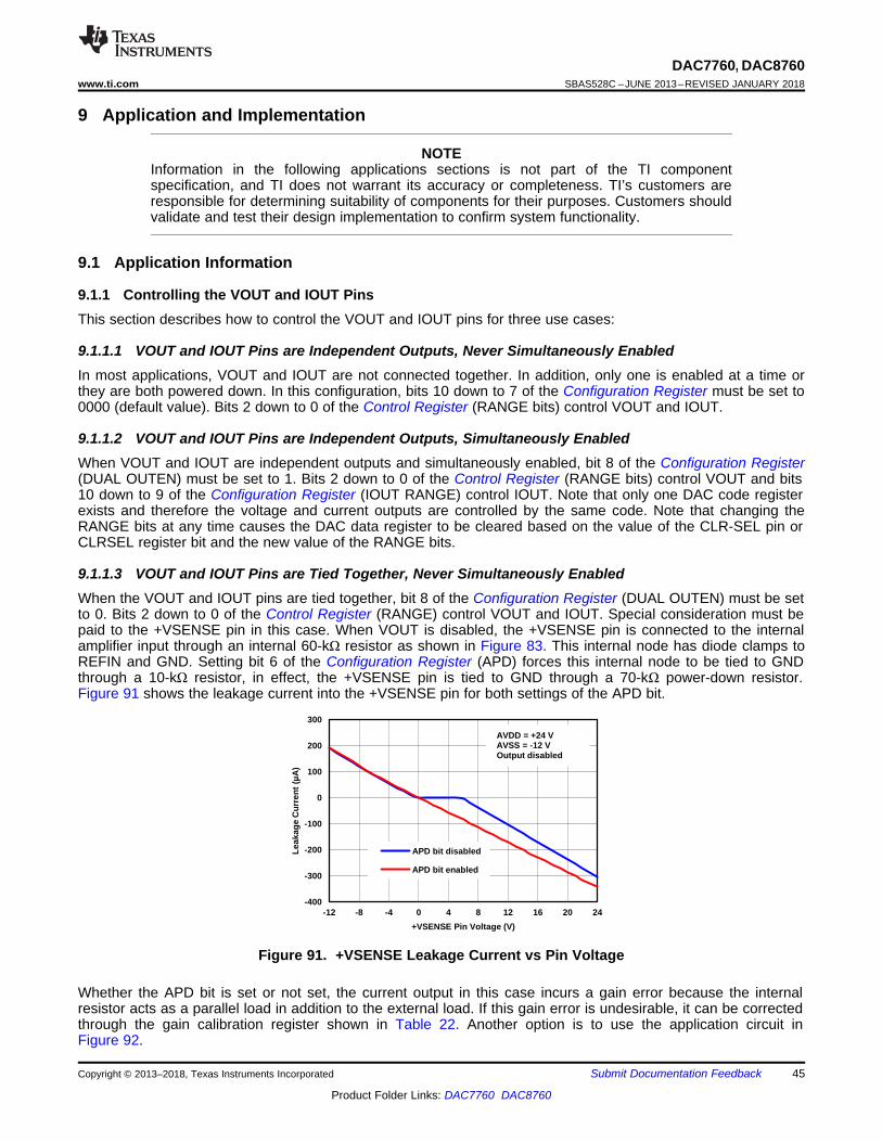
-400
-300
-200
-100
0
100
200
300
-12 -8 -4 0 4 8 12 16 20 24
Leak
age
Cur
rent
(µA
)
+VSENSE Pin Voltage (V)
APD bit disabled
APD bit enabled
C002
AVDD = +24 V AVSS = -12 V Output disabled
45
DAC7760, DAC8760www.ti.com SBAS528C –JUNE 2013–REVISED JANUARY 2018
Product Folder Links: DAC7760 DAC8760
Submit Documentation FeedbackCopyright © 2013–2018, Texas Instruments Incorporated
9 Application and Implementation
NOTEInformation in the following applications sections is not part of the TI componentspecification, and TI does not warrant its accuracy or completeness. TI’s customers areresponsible for determining suitability of components for their purposes. Customers shouldvalidate and test their design implementation to confirm system functionality.
9.1 Application Information
9.1.1 Controlling the VOUT and IOUT PinsThis section describes how to control the VOUT and IOUT pins for three use cases:
9.1.1.1 VOUT and IOUT Pins are Independent Outputs, Never Simultaneously EnabledIn most applications, VOUT and IOUT are not connected together. In addition, only one is enabled at a time orthey are both powered down. In this configuration, bits 10 down to 7 of the Configuration Register must be set to0000 (default value). Bits 2 down to 0 of the Control Register (RANGE bits) control VOUT and IOUT.
9.1.1.2 VOUT and IOUT Pins are Independent Outputs, Simultaneously EnabledWhen VOUT and IOUT are independent outputs and simultaneously enabled, bit 8 of the Configuration Register(DUAL OUTEN) must be set to 1. Bits 2 down to 0 of the Control Register (RANGE bits) control VOUT and bits10 down to 9 of the Configuration Register (IOUT RANGE) control IOUT. Note that only one DAC code registerexists and therefore the voltage and current outputs are controlled by the same code. Note that changing theRANGE bits at any time causes the DAC data register to be cleared based on the value of the CLR-SEL pin orCLRSEL register bit and the new value of the RANGE bits.
9.1.1.3 VOUT and IOUT Pins are Tied Together, Never Simultaneously EnabledWhen the VOUT and IOUT pins are tied together, bit 8 of the Configuration Register (DUAL OUTEN) must be setto 0. Bits 2 down to 0 of the Control Register (RANGE) control VOUT and IOUT. Special consideration must bepaid to the +VSENSE pin in this case. When VOUT is disabled, the +VSENSE pin is connected to the internalamplifier input through an internal 60-kΩ resistor as shown in Figure 83. This internal node has diode clamps toREFIN and GND. Setting bit 6 of the Configuration Register (APD) forces this internal node to be tied to GNDthrough a 10-kΩ resistor, in effect, the +VSENSE pin is tied to GND through a 70-kΩ power-down resistor.Figure 91 shows the leakage current into the +VSENSE pin for both settings of the APD bit.
Figure 91. +VSENSE Leakage Current vs Pin Voltage
Whether the APD bit is set or not set, the current output in this case incurs a gain error because the internalresistor acts as a parallel load in addition to the external load. If this gain error is undesirable, it can be correctedthrough the gain calibration register shown in Table 22. Another option is to use the application circuit inFigure 92.
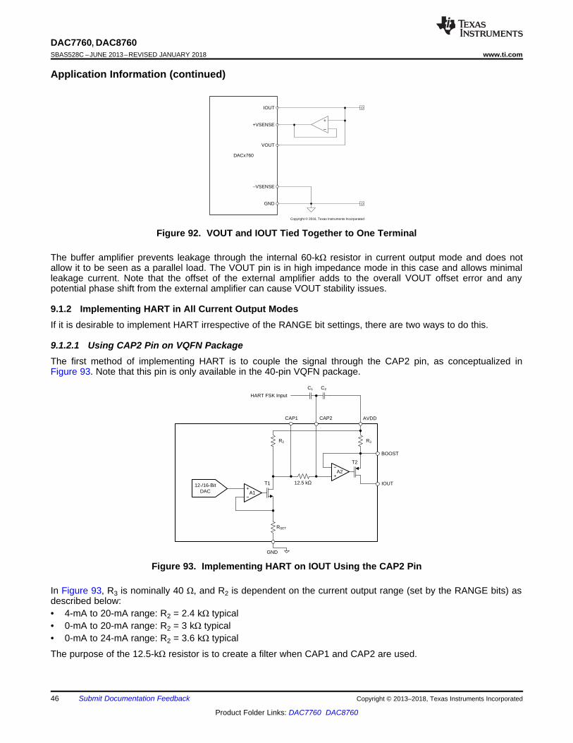
+12-/16-BitBa_
DACBa_
RSET
R2
T1
A1
+
T2
A2
R3
í
í
12.5 k
HART FSK Input
C1 C2
CAP2CAP1 AVDD
GND
IOUT
BOOST
DACx760
IOUT
+VSENSE
GND
±VSENSE
VOUT
+
±
Copyright © 2016, Texas Instruments Incorporated
46
DAC7760, DAC8760SBAS528C –JUNE 2013–REVISED JANUARY 2018 www.ti.com
Product Folder Links: DAC7760 DAC8760
Submit Documentation Feedback Copyright © 2013–2018, Texas Instruments Incorporated
Application Information (continued)
Figure 92. VOUT and IOUT Tied Together to One Terminal
The buffer amplifier prevents leakage through the internal 60-kΩ resistor in current output mode and does notallow it to be seen as a parallel load. The VOUT pin is in high impedance mode in this case and allows minimalleakage current. Note that the offset of the external amplifier adds to the overall VOUT offset error and anypotential phase shift from the external amplifier can cause VOUT stability issues.
9.1.2 Implementing HART in All Current Output ModesIf it is desirable to implement HART irrespective of the RANGE bit settings, there are two ways to do this.
9.1.2.1 Using CAP2 Pin on VQFN PackageThe first method of implementing HART is to couple the signal through the CAP2 pin, as conceptualized inFigure 93. Note that this pin is only available in the 40-pin VQFN package.
Figure 93. Implementing HART on IOUT Using the CAP2 Pin
In Figure 93, R3 is nominally 40 Ω, and R2 is dependent on the current output range (set by the RANGE bits) asdescribed below:• 4-mA to 20-mA range: R2 = 2.4 kΩ typical• 0-mA to 20-mA range: R2 = 3 kΩ typical• 0-mA to 24-mA range: R2 = 3.6 kΩ typical
The purpose of the 12.5-kΩ resistor is to create a filter when CAP1 and CAP2 are used.

T2
T1DAC
CAP1 CAP2 AVDD
IOUT
ISET-R
HART Signal Conditioning
HART-IN
R1
R3
R2
(ON Only in 4-mA to 20-mA Range)
CinHART SIGNAL
RSET
15 N
Rin
S1
+A1
+
A2
47
DAC7760, DAC8760www.ti.com SBAS528C –JUNE 2013–REVISED JANUARY 2018
Product Folder Links: DAC7760 DAC8760
Submit Documentation FeedbackCopyright © 2013–2018, Texas Instruments Incorporated
Application Information (continued)To insert the external HART signal on the CAP2 pin, an external ac-coupling capacitor is typically connected toCAP2. The high-pass filter 3-dB frequency would be determined by the resistive impedance looking into CAP2(R2 + 12.5 kΩ) and the coupling capacitor value. The 3-dB frequency would be 1 /(2 × π × [R2 + 12.5 kΩ] ×[Coupling Cap Value]).
After the input HART frequency is greater than the 3-dB frequency, the ac signal is seen at the plus input ofamplifier A2 and would therefore be seen across the 40-Ω resistor. To generate a 1-mA signal on the outputwould therefore require a 40-mV peak-to-peak signal on CAP2. Because most HART modems do not output a40-mV signal, a capacitive divider is used in the above circuit to attenuate the FSK signal from the modem. In theabove circuit, the high-pass cutoff frequency would be 1 / (2 × π × [R2+12.5 kΩ] × [C1 + C2]). There is onedisadvantage of this approach: if the AVDD supply was not clean, any ripple on it could couple into the part.
9.1.2.2 Using the ISET-R PinThe second method to implement HART is to couple the HART signal through the ISET-R pin when IOUT isoperated using an external RSET resistor. The FSK signal from the modem is ac coupled into the pin through aseries combination of Rin and Cin as shown in Figure 94.
Figure 94. Implementing HART With the ISET-R pin
The magnitude of the ac current output is calculated as (VHART × k) / Rin, where k is a constant that representsthe gain transfer function from the ISET-R pin to the IOUT pin and depends on the selected current output rangeas follows: k = 60 for the 4-mA to 20-mA range, 75 for the 0-mA to 20-mA range, and 90 for the 0-mA to 24-mArange. The series input resistor and capacitor form a high-pass filter at the ISET-R pin and Cin must be selectedto make sure that all signals in the HART extended-frequency band pass through unattenuated.
9.1.3 Short-Circuit Current LimitingThe DACx760 voltage output includes an internal circuit to typically regulate the load current to about 30 mA.However, this parameter is not production tested or trimmed. Optionally, users can use an external currentlimiting circuit on VOUT. However, if the VOUT, IOUT and +VSENSE pins are tied together, this circuit must beplaced in the VOUT path before it is tied together to the other pins at the common terminal. The nature of thecurrent-limiting circuit depends on the application and load. An example of a unidirectional current limiter isshown in Figure 95.
R1
R2 R3
R4
D1Q1
Q2
VIN
VOUT
48
DAC7760, DAC8760SBAS528C –JUNE 2013–REVISED JANUARY 2018 www.ti.com
Product Folder Links: DAC7760 DAC8760
Submit Documentation Feedback Copyright © 2013–2018, Texas Instruments Incorporated
Application Information (continued)
Figure 95. Unidirectional Current Limiter Circuit
Under normal operation, most current in this circuit flows through Q1 and into R3. As current increases throughR3, so does the voltage drop across R3, which increases the base-emitter voltage of Q2. Eventually the base-emitter voltage of Q2 becomes high enough to turn on Q2, which turns off Q1 and reduce the current that canpass from VIN to VOUT. The value of R3 sets the current limit. Note that this is a very simple example and onlyapplies for sourcing current into a resistive load. For cases involving both sourcing and sinking current as well asnonresistive loads, more complex circuits are required to achieve bidirectional current limiting.
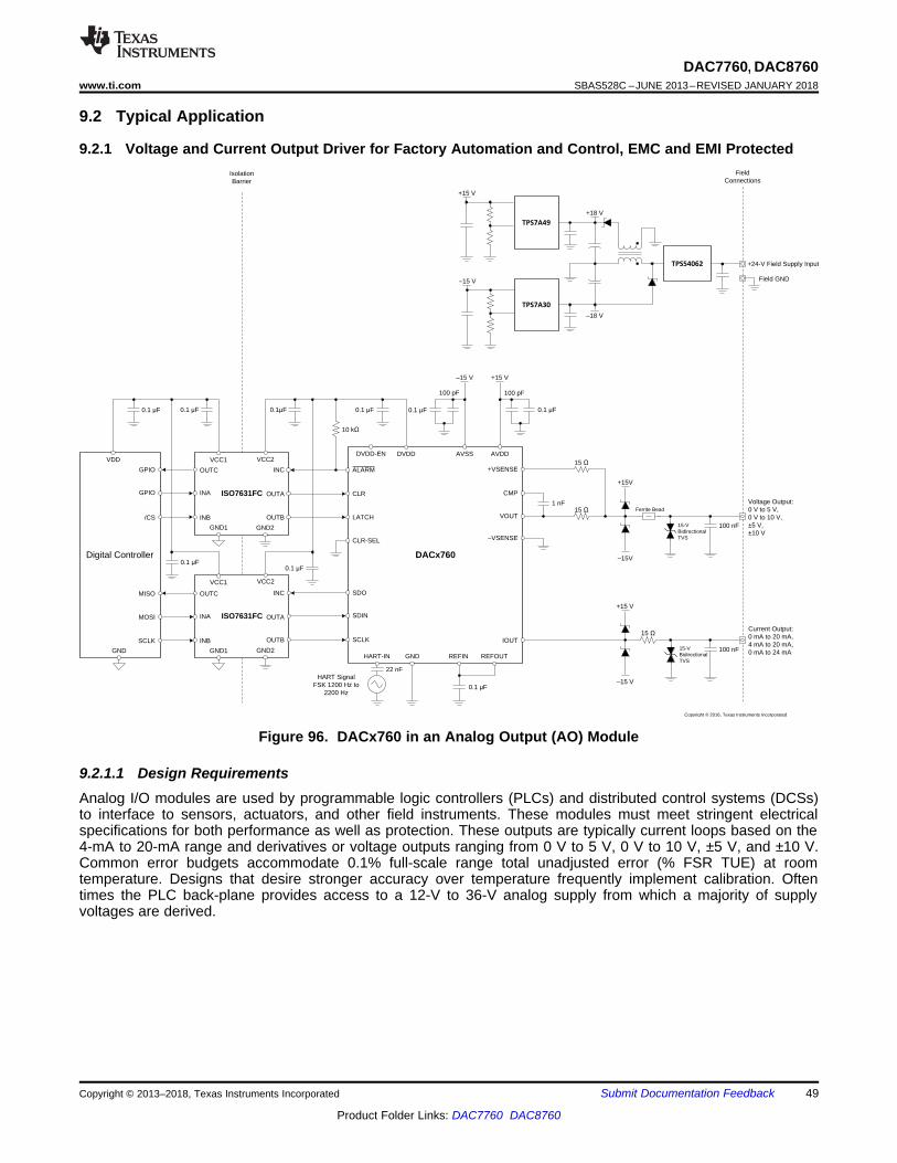
ISO7631FC
DACx760
IOUT
Voltage Output:0 V to 5 V,0 V to 10 V,±5 V,±10 V
Current Output:0 mA to 20 mA,4 mA to 20 mA,0 mA to 24 mA
+15V
±15V
15-V Bidirectional TVS
+15 V
±15 V
15-V Bidirectional TVS
Ferrite Bead
100 nF
100 nF
15
15
15
1 nF
±VSENSE
VOUT
CMP
+VSENSE
REFIN REFOUTGNDHART-IN
HART SignalFSK 1200 Hz to
2200 Hz
AVSS AVDDDVDDDVDD-EN
+15 V±15 V
0.1 F
0.1 F
22 nF
100 pF
0.1 F
100 pF
0.1 F
SCLK
SDIN
SDO
CLR-SEL
LATCH
CLR
ALARM
10 N
INC
OUTA
OUTB
VCC2
GND2
0.1F
0.1 F
ISO7631FC
INC
OUTA
OUTB
VCC2
GND2
VCC1
GND1
OUTC
INA
INB
VCC1
GND1
OUTC
INA
INB
Digital Controller
GND
VDD
0.1 F0.1 F
0.1 F
SCLK
MOSI
MISO
/CS
GPIO
GPIO
Isolation Barrier
TPS54062 +24-V Field Supply Input
Field GND
+18 V
±18 V
TPS7A30
TPS7A49
±15 V
+15 V
Field Connections
Copyright © 2016, Texas Instruments Incorporated
49
DAC7760, DAC8760www.ti.com SBAS528C –JUNE 2013–REVISED JANUARY 2018
Product Folder Links: DAC7760 DAC8760
Submit Documentation FeedbackCopyright © 2013–2018, Texas Instruments Incorporated
9.2 Typical Application
9.2.1 Voltage and Current Output Driver for Factory Automation and Control, EMC and EMI Protected
Figure 96. DACx760 in an Analog Output (AO) Module
9.2.1.1 Design RequirementsAnalog I/O modules are used by programmable logic controllers (PLCs) and distributed control systems (DCSs)to interface to sensors, actuators, and other field instruments. These modules must meet stringent electricalspecifications for both performance as well as protection. These outputs are typically current loops based on the4-mA to 20-mA range and derivatives or voltage outputs ranging from 0 V to 5 V, 0 V to 10 V, ±5 V, and ±10 V.Common error budgets accommodate 0.1% full-scale range total unadjusted error (% FSR TUE) at roomtemperature. Designs that desire stronger accuracy over temperature frequently implement calibration. Oftentimes the PLC back-plane provides access to a 12-V to 36-V analog supply from which a majority of supplyvoltages are derived.
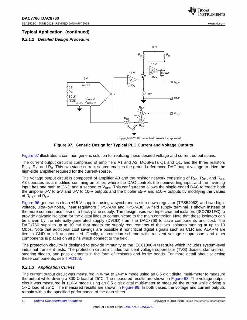
IOUT
15 V
RA RB
RSET
Q1
Q2
A1
A2
VOUT
GND
A3
RFB
RG1
AVDD
V /
VREFIN
REFOUTGND
DIN
SCLK
CS
LDAC
15 V
-15 V
15 V
-15 V
15 V
-15 V
5 V
RG2
+
+
+
Copyright © 2016, Texas Instruments Incorporated
50
DAC7760, DAC8760SBAS528C –JUNE 2013–REVISED JANUARY 2018 www.ti.com
Product Folder Links: DAC7760 DAC8760
Submit Documentation Feedback Copyright © 2013–2018, Texas Instruments Incorporated
Typical Application (continued)9.2.1.2 Detailed Design Procedure
Figure 97. Generic Design for Typical PLC Current and Voltage Outputs
Figure 97 illustrates a common generic solution for realizing these desired voltage and current output spans.
The current output circuit is comprised of amplifiers A1 and A2, MOSFETs Q1 and Q1, and the three resistorsRSET, RA, and RB. This two-stage current source enables the ground-referenced DAC output voltage to drive thehigh-side amplifier required for the current-source.
The voltage output circuit is composed of amplifier A3 and the resistor network consisting of RFB, RG1, and RG2.A3 operates as a modified summing amplifier, where the DAC controls the noninverting input and the invertinginput has one path to GND and a second to VREF. This configuration allows the single-ended DAC to create boththe unipolar 0-V to 5-V and 0-V to 10-V outputs and the bipolar ±5-V and ±10-V outputs by modifying the valuesof RG1 and RG2.
Figure 96 generates clean ±15-V supplies using a synchronous step-down regulator (TPS54062) and two high-voltage, ultra-low noise, linear regulators (TPS7A49 and TPS7A30). A field supply terminal is shown instead ofthe more common use case of a back-plane supply. The design uses two triple channel isolators (ISO7631FC) toprovide galvanic isolation for the digital lines to communicate to the main controller. Note that these isolators canbe driven by the internally-generated supply (DVDD) from the DACx760 to save components and cost. TheDACx760 supplies up to 10 mA that meets the supply requirements of the two isolators running at up to 10Mbps. Note that additional cost savings are possible if noncritical digital signals such as CLR and ALARM aretied to GND or left unconnected. Finally, a protection scheme with transient voltage suppressors and othercomponents is placed on all pins which connect to the field.
The protection circuitry is designed to provide immunity to the IEC61000-4 test suite which includes system-levelindustrial transient tests. The protection circuit includes transient voltage suppressor (TVS) diodes, clamp-to-railsteering diodes, and pass elements in the form of resistors and ferrite beads. For more detail about selectingthese components, see TIPD153.
9.2.1.3 Application CurvesThe current output circuit was measured in 0-mA to 24-mA mode using an 8.5 digit digital multi-meter to measurethe output while driving a 300-Ω load at 25°C. The measured results are shown in Figure 98. The voltage outputcircuit was measured in ±10-V mode using an 8.5 digit digital multi-meter to measure the output while driving a1-kΩ load at 25°C. The measured results are shown in Figure 99. In both cases, the voltage and current outputsremain within the specified performance of the data sheet.
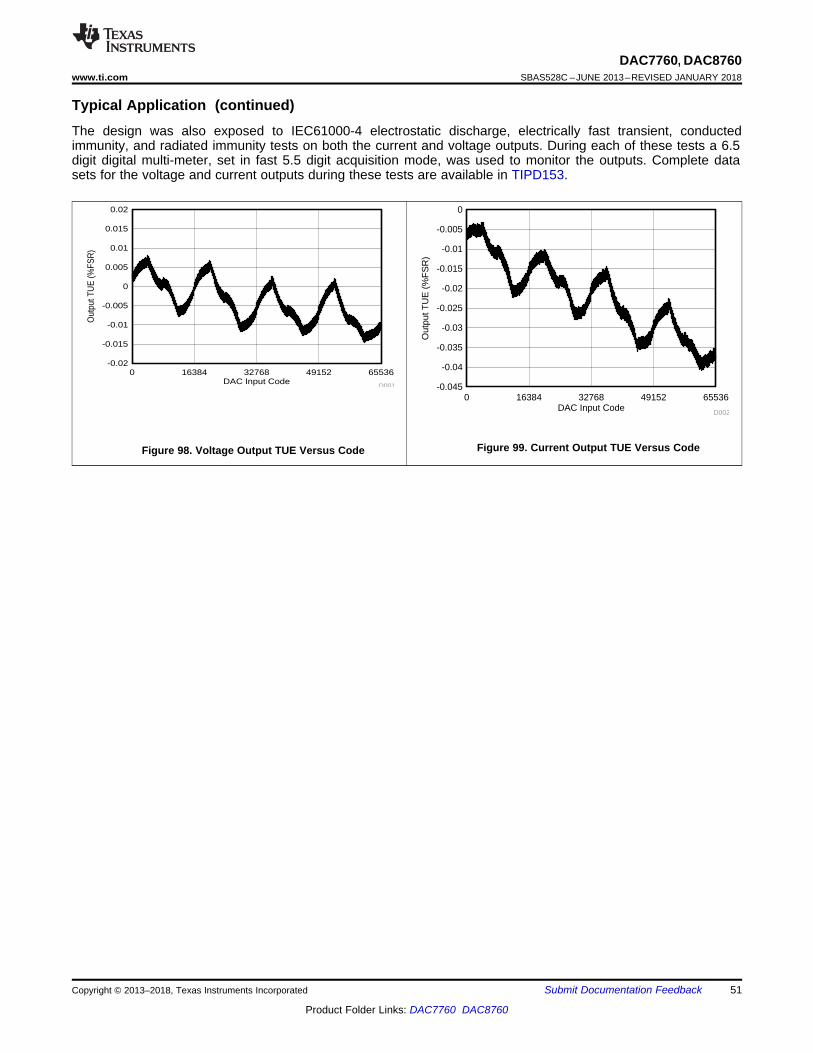
DAC Input Code
Out
put T
UE
(%
FS
R)
0 16384 32768 49152 65536-0.045
-0.04
-0.035
-0.03
-0.025
-0.02
-0.015
-0.01
-0.005
0
D002
DAC Input Code
Out
put T
UE
(%FS
R)
0 16384 32768 49152 65536-0.02
-0.015
-0.01
-0.005
0
0.005
0.01
0.015
0.02
D001
51
DAC7760, DAC8760www.ti.com SBAS528C –JUNE 2013–REVISED JANUARY 2018
Product Folder Links: DAC7760 DAC8760
Submit Documentation FeedbackCopyright © 2013–2018, Texas Instruments Incorporated
Typical Application (continued)The design was also exposed to IEC61000-4 electrostatic discharge, electrically fast transient, conductedimmunity, and radiated immunity tests on both the current and voltage outputs. During each of these tests a 6.5digit digital multi-meter, set in fast 5.5 digit acquisition mode, was used to monitor the outputs. Complete datasets for the voltage and current outputs during these tests are available in TIPD153.
Figure 98. Voltage Output TUE Versus Code Figure 99. Current Output TUE Versus Code
52
DAC7760, DAC8760SBAS528C –JUNE 2013–REVISED JANUARY 2018 www.ti.com
Product Folder Links: DAC7760 DAC8760
Submit Documentation Feedback Copyright © 2013–2018, Texas Instruments Incorporated
10 Power Supply RecommendationsThe DACx760 family can operate within the specified single-supply range of 10 V to 36 V applied to the AVDDpin or the specified dual-supply range of 10 V to 18 V applied to AVDD and 0 V to –18 V on AVSS or anysubsequent combination that does not exceed the maximum difference of 36 V between AVDD and AVSS. Thedigital supply, DVDD, can operate within the specified supply range of 2.7 V to 5.5 V or be powered by theinternal 4.6-V LDO. Switching power supplies and DC/DC converters often have high-frequency glitches orspikes riding on the output voltage. In addition, digital components can create similar high frequency spikes. Thisnoise can be easily coupled into the DAC output voltage or current through various paths between the powerconnections and analog output. To further reduce noise, TI recommends including bulk and local decouplingcapacitors. The current consumption on the AVDD and AVSS pins, the short-circuit current limit for the voltageoutput, and current ranges for the current output, are listed in Electrical Characteristics. The power supply mustmeet the requirements listed in Electrical Characteristics.
11 Layout
11.1 Layout GuidelinesTo maximize the performance of the DACx760 in any application, good layout practices and proper circuit designmust be followed. A few recommendations specific to the DACx760 are:1. As is seen in Figure 93, CAP2 is directly connected to the input of the final IOUT amplifier. Any noise or
unwanted ac signal routed near the CAP1 and/or CAP2 pins could capacitively couple onto internal nodesand affect IOUT. Therefore, with the QFN package, it is important to avoid routing any digital or HART signaltrace over the CAP1 and CAP2 traces.
2. The thermal PAD must be connected to the lowest potential in the system.3. The +VSENSE connection must be a low-impedance trace connected close to the point of load.4. AVDD and AVSS must have decoupling capacitors local to the respective pins.5. The reference capacitor must be placed close to the reference input pin.6. Avoid routing switching signals near the reference input.7. For designs that include protection circuits:
a. Place diversion elements, such as TVS diodes or capacitors, close to off-board connectors to make surethat return current from high-energy transients does not cause damage to sensitive devices.
b. Use large, wide traces to provide a low-impedance path to divert high-energy transients away from I/Oterminals.

GND
AVSS AVDD
Digital I/O
Analog Supply Decoupling
Digital Supply
Decoupling
Analo
g S
upply
Decouplin
g
External RSET
(Optional)
CA
P1 / C
AP
2
(Optional)
CM
PC
AP
(Optional)
BOOST Configuration
(Optional)
53
DAC7760, DAC8760www.ti.com SBAS528C –JUNE 2013–REVISED JANUARY 2018
Product Folder Links: DAC7760 DAC8760
Submit Documentation FeedbackCopyright © 2013–2018, Texas Instruments Incorporated
11.2 Layout Example
Figure 100. DACx760 Layout Example
11.3 Thermal ConsiderationsThe DACx760 is designed for a maximum junction temperature of +150°C. In cases where the maximum AVDDis driving maximum current into ground, this could be exceeded. Use the following equation, from the AbsoluteMaximum Ratings, to determine the maximum junction temperature that can be reached:
Power Dissipation = (TJmax – TA)/θJA
where• TJmax = 150°C• TA is the ambient temperature• θJA is the package dependent junction-to-ambient thermal resistance, which is found in Thermal Information (8)
The power dissipation can be calculated by multiplying all the supply voltages with the currents supplied, which isfound in the Power Requirements subsection of Electrical Characteristics.
Consider an example: IOUT is enabled, supplying 24 mA into GND with a 25°C ambient temperature, AVDD of24 V, AVSS is tied to GND and DVDD is generated internally. From the specifications table, the maximum valueof AIDD = 3 mA when IOUT is enabled and DAC code = 0x0000. Also, the maximum value of DIDD = 1 mA.Accordingly, the worst case power dissipation is 24 V × (24 mA + 3 mA + 1 mA) = 672 mW. Using the RθJA valuefor the TSSOP package, we get TJmax = 25°C + (32.3 × 0.672)°C = 46.7°C. At 85°C ambient temperature, thecorresponding value of TJmax is 106.7°C. Using this type of analysis, the system designer can both specify anddesign for the equipment operating conditions. Note that the thermal pad in both packages is recommended tobe connected to a copper plane for enhanced thermal performance.

54
DAC7760, DAC8760SBAS528C –JUNE 2013–REVISED JANUARY 2018 www.ti.com
Product Folder Links: DAC7760 DAC8760
Submit Documentation Feedback Copyright © 2013–2018, Texas Instruments Incorporated
12 Device and Documentation Support
12.1 Related LinksThe table below lists quick access links. Categories include technical documents, support and communityresources, tools and software, and quick access to order now.
Table 26. Related Links
PARTS PRODUCT FOLDER ORDER NOW TECHNICALDOCUMENTS
TOOLS &SOFTWARE
SUPPORT &COMMUNITY
DAC7760 Click here Click here Click here Click here Click hereDAC8760 Click here Click here Click here Click here Click here
12.2 Receiving Notification of Documentation UpdatesTo receive notification of documentation updates, navigate to the device product folder on ti.com. In the upperright corner, click on Alert me to register and receive a weekly digest of any product information that haschanged. For change details, review the revision history included in any revised document.
12.3 Community ResourceThe following links connect to TI community resources. Linked contents are provided "AS IS" by the respectivecontributors. They do not constitute TI specifications and do not necessarily reflect TI's views; see TI's Terms ofUse.
TI E2E™ Online Community TI's Engineer-to-Engineer (E2E) Community. Created to foster collaborationamong engineers. At e2e.ti.com, you can ask questions, share knowledge, explore ideas and helpsolve problems with fellow engineers.
Design Support TI's Design Support Quickly find helpful E2E forums along with design support tools andcontact information for technical support.
12.4 TrademarksE2E is a trademark of Texas Instruments.HART is a registered trademark of HART Communication Foundation.SPI, QSPI are trademarks of Motorola, Inc.All other trademarks are the property of their respective owners.
12.5 Electrostatic Discharge CautionThis integrated circuit can be damaged by ESD. Texas Instruments recommends that all integrated circuits be handled withappropriate precautions. Failure to observe proper handling and installation procedures can cause damage.
ESD damage can range from subtle performance degradation to complete device failure. Precision integrated circuits may be moresusceptible to damage because very small parametric changes could cause the device not to meet its published specifications.
12.6 GlossarySLYZ022 — TI Glossary.
This glossary lists and explains terms, acronyms, and definitions.
13 Mechanical, Packaging, and Orderable InformationThe following pages include mechanical, packaging, and orderable information. This information is the mostcurrent data available for the designated devices. This data is subject to change without notice and revision ofthis document. For browser-based versions of this data sheet, refer to the left-hand navigation.
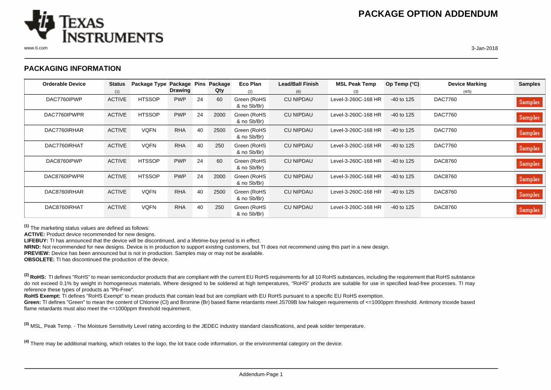
PACKAGE OPTION ADDENDUM
www.ti.com 3-Jan-2018
Addendum-Page 1
PACKAGING INFORMATION
Orderable Device Status(1)
Package Type PackageDrawing
Pins PackageQty
Eco Plan(2)
Lead/Ball Finish(6)
MSL Peak Temp(3)
Op Temp (°C) Device Marking(4/5)
Samples
DAC7760IPWP ACTIVE HTSSOP PWP 24 60 Green (RoHS& no Sb/Br)
CU NIPDAU Level-3-260C-168 HR -40 to 125 DAC7760
DAC7760IPWPR ACTIVE HTSSOP PWP 24 2000 Green (RoHS& no Sb/Br)
CU NIPDAU Level-3-260C-168 HR -40 to 125 DAC7760
DAC7760IRHAR ACTIVE VQFN RHA 40 2500 Green (RoHS& no Sb/Br)
CU NIPDAU Level-3-260C-168 HR -40 to 125 DAC7760
DAC7760IRHAT ACTIVE VQFN RHA 40 250 Green (RoHS& no Sb/Br)
CU NIPDAU Level-3-260C-168 HR -40 to 125 DAC7760
DAC8760IPWP ACTIVE HTSSOP PWP 24 60 Green (RoHS& no Sb/Br)
CU NIPDAU Level-3-260C-168 HR -40 to 125 DAC8760
DAC8760IPWPR ACTIVE HTSSOP PWP 24 2000 Green (RoHS& no Sb/Br)
CU NIPDAU Level-3-260C-168 HR -40 to 125 DAC8760
DAC8760IRHAR ACTIVE VQFN RHA 40 2500 Green (RoHS& no Sb/Br)
CU NIPDAU Level-3-260C-168 HR -40 to 125 DAC8760
DAC8760IRHAT ACTIVE VQFN RHA 40 250 Green (RoHS& no Sb/Br)
CU NIPDAU Level-3-260C-168 HR -40 to 125 DAC8760
(1) The marketing status values are defined as follows:ACTIVE: Product device recommended for new designs.LIFEBUY: TI has announced that the device will be discontinued, and a lifetime-buy period is in effect.NRND: Not recommended for new designs. Device is in production to support existing customers, but TI does not recommend using this part in a new design.PREVIEW: Device has been announced but is not in production. Samples may or may not be available.OBSOLETE: TI has discontinued the production of the device.
(2) RoHS: TI defines "RoHS" to mean semiconductor products that are compliant with the current EU RoHS requirements for all 10 RoHS substances, including the requirement that RoHS substancedo not exceed 0.1% by weight in homogeneous materials. Where designed to be soldered at high temperatures, "RoHS" products are suitable for use in specified lead-free processes. TI mayreference these types of products as "Pb-Free".RoHS Exempt: TI defines "RoHS Exempt" to mean products that contain lead but are compliant with EU RoHS pursuant to a specific EU RoHS exemption.Green: TI defines "Green" to mean the content of Chlorine (Cl) and Bromine (Br) based flame retardants meet JS709B low halogen requirements of <=1000ppm threshold. Antimony trioxide basedflame retardants must also meet the <=1000ppm threshold requirement.
(3) MSL, Peak Temp. - The Moisture Sensitivity Level rating according to the JEDEC industry standard classifications, and peak solder temperature.
(4) There may be additional marking, which relates to the logo, the lot trace code information, or the environmental category on the device.
PACKAGE OPTION ADDENDUM
www.ti.com 3-Jan-2018
Addendum-Page 2
(5) Multiple Device Markings will be inside parentheses. Only one Device Marking contained in parentheses and separated by a "~" will appear on a device. If a line is indented then it is a continuationof the previous line and the two combined represent the entire Device Marking for that device.
(6) Lead/Ball Finish - Orderable Devices may have multiple material finish options. Finish options are separated by a vertical ruled line. Lead/Ball Finish values may wrap to two lines if the finishvalue exceeds the maximum column width.
Important Information and Disclaimer:The information provided on this page represents TI's knowledge and belief as of the date that it is provided. TI bases its knowledge and belief on informationprovided by third parties, and makes no representation or warranty as to the accuracy of such information. Efforts are underway to better integrate information from third parties. TI has taken andcontinues to take reasonable steps to provide representative and accurate information but may not have conducted destructive testing or chemical analysis on incoming materials and chemicals.TI and TI suppliers consider certain information to be proprietary, and thus CAS numbers and other limited information may not be available for release.
In no event shall TI's liability arising out of such information exceed the total purchase price of the TI part(s) at issue in this document sold by TI to Customer on an annual basis.
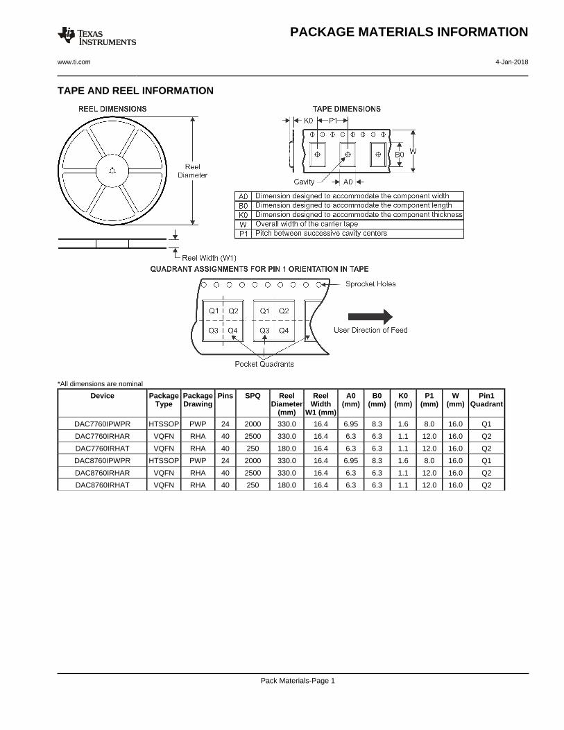
TAPE AND REEL INFORMATION
*All dimensions are nominal
Device PackageType
PackageDrawing
Pins SPQ ReelDiameter
(mm)
ReelWidth
W1 (mm)
A0(mm)
B0(mm)
K0(mm)
P1(mm)
W(mm)
Pin1Quadrant
DAC7760IPWPR HTSSOP PWP 24 2000 330.0 16.4 6.95 8.3 1.6 8.0 16.0 Q1
DAC7760IRHAR VQFN RHA 40 2500 330.0 16.4 6.3 6.3 1.1 12.0 16.0 Q2
DAC7760IRHAT VQFN RHA 40 250 180.0 16.4 6.3 6.3 1.1 12.0 16.0 Q2
DAC8760IPWPR HTSSOP PWP 24 2000 330.0 16.4 6.95 8.3 1.6 8.0 16.0 Q1
DAC8760IRHAR VQFN RHA 40 2500 330.0 16.4 6.3 6.3 1.1 12.0 16.0 Q2
DAC8760IRHAT VQFN RHA 40 250 180.0 16.4 6.3 6.3 1.1 12.0 16.0 Q2
PACKAGE MATERIALS INFORMATION
www.ti.com 4-Jan-2018
Pack Materials-Page 1
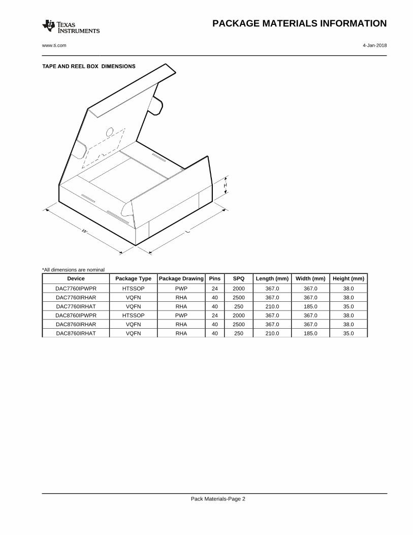
*All dimensions are nominal
Device Package Type Package Drawing Pins SPQ Length (mm) Width (mm) Height (mm)
DAC7760IPWPR HTSSOP PWP 24 2000 367.0 367.0 38.0
DAC7760IRHAR VQFN RHA 40 2500 367.0 367.0 38.0
DAC7760IRHAT VQFN RHA 40 250 210.0 185.0 35.0
DAC8760IPWPR HTSSOP PWP 24 2000 367.0 367.0 38.0
DAC8760IRHAR VQFN RHA 40 2500 367.0 367.0 38.0
DAC8760IRHAT VQFN RHA 40 250 210.0 185.0 35.0
PACKAGE MATERIALS INFORMATION
www.ti.com 4-Jan-2018
Pack Materials-Page 2
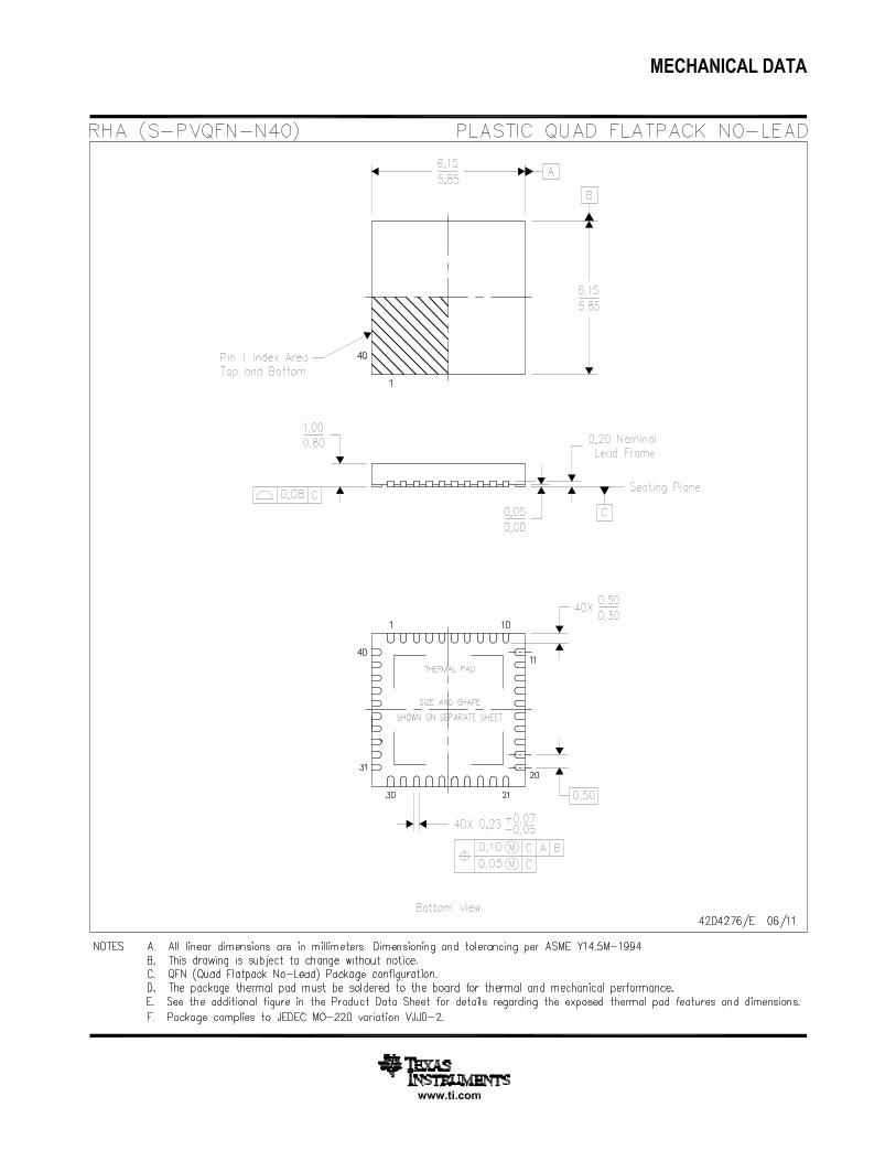
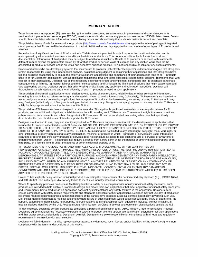
IMPORTANT NOTICE
Texas Instruments Incorporated (TI) reserves the right to make corrections, enhancements, improvements and other changes to itssemiconductor products and services per JESD46, latest issue, and to discontinue any product or service per JESD48, latest issue. Buyersshould obtain the latest relevant information before placing orders and should verify that such information is current and complete.TI’s published terms of sale for semiconductor products (http://www.ti.com/sc/docs/stdterms.htm) apply to the sale of packaged integratedcircuit products that TI has qualified and released to market. Additional terms may apply to the use or sale of other types of TI products andservices.Reproduction of significant portions of TI information in TI data sheets is permissible only if reproduction is without alteration and isaccompanied by all associated warranties, conditions, limitations, and notices. TI is not responsible or liable for such reproduceddocumentation. Information of third parties may be subject to additional restrictions. Resale of TI products or services with statementsdifferent from or beyond the parameters stated by TI for that product or service voids all express and any implied warranties for theassociated TI product or service and is an unfair and deceptive business practice. TI is not responsible or liable for any such statements.Buyers and others who are developing systems that incorporate TI products (collectively, “Designers”) understand and agree that Designersremain responsible for using their independent analysis, evaluation and judgment in designing their applications and that Designers havefull and exclusive responsibility to assure the safety of Designers' applications and compliance of their applications (and of all TI productsused in or for Designers’ applications) with all applicable regulations, laws and other applicable requirements. Designer represents that, withrespect to their applications, Designer has all the necessary expertise to create and implement safeguards that (1) anticipate dangerousconsequences of failures, (2) monitor failures and their consequences, and (3) lessen the likelihood of failures that might cause harm andtake appropriate actions. Designer agrees that prior to using or distributing any applications that include TI products, Designer willthoroughly test such applications and the functionality of such TI products as used in such applications.TI’s provision of technical, application or other design advice, quality characterization, reliability data or other services or information,including, but not limited to, reference designs and materials relating to evaluation modules, (collectively, “TI Resources”) are intended toassist designers who are developing applications that incorporate TI products; by downloading, accessing or using TI Resources in anyway, Designer (individually or, if Designer is acting on behalf of a company, Designer’s company) agrees to use any particular TI Resourcesolely for this purpose and subject to the terms of this Notice.TI’s provision of TI Resources does not expand or otherwise alter TI’s applicable published warranties or warranty disclaimers for TIproducts, and no additional obligations or liabilities arise from TI providing such TI Resources. TI reserves the right to make corrections,enhancements, improvements and other changes to its TI Resources. TI has not conducted any testing other than that specificallydescribed in the published documentation for a particular TI Resource.Designer is authorized to use, copy and modify any individual TI Resource only in connection with the development of applications thatinclude the TI product(s) identified in such TI Resource. NO OTHER LICENSE, EXPRESS OR IMPLIED, BY ESTOPPEL OR OTHERWISETO ANY OTHER TI INTELLECTUAL PROPERTY RIGHT, AND NO LICENSE TO ANY TECHNOLOGY OR INTELLECTUAL PROPERTYRIGHT OF TI OR ANY THIRD PARTY IS GRANTED HEREIN, including but not limited to any patent right, copyright, mask work right, orother intellectual property right relating to any combination, machine, or process in which TI products or services are used. Informationregarding or referencing third-party products or services does not constitute a license to use such products or services, or a warranty orendorsement thereof. Use of TI Resources may require a license from a third party under the patents or other intellectual property of thethird party, or a license from TI under the patents or other intellectual property of TI.TI RESOURCES ARE PROVIDED “AS IS” AND WITH ALL FAULTS. TI DISCLAIMS ALL OTHER WARRANTIES ORREPRESENTATIONS, EXPRESS OR IMPLIED, REGARDING RESOURCES OR USE THEREOF, INCLUDING BUT NOT LIMITED TOACCURACY OR COMPLETENESS, TITLE, ANY EPIDEMIC FAILURE WARRANTY AND ANY IMPLIED WARRANTIES OFMERCHANTABILITY, FITNESS FOR A PARTICULAR PURPOSE, AND NON-INFRINGEMENT OF ANY THIRD PARTY INTELLECTUALPROPERTY RIGHTS. TI SHALL NOT BE LIABLE FOR AND SHALL NOT DEFEND OR INDEMNIFY DESIGNER AGAINST ANY CLAIM,INCLUDING BUT NOT LIMITED TO ANY INFRINGEMENT CLAIM THAT RELATES TO OR IS BASED ON ANY COMBINATION OFPRODUCTS EVEN IF DESCRIBED IN TI RESOURCES OR OTHERWISE. IN NO EVENT SHALL TI BE LIABLE FOR ANY ACTUAL,DIRECT, SPECIAL, COLLATERAL, INDIRECT, PUNITIVE, INCIDENTAL, CONSEQUENTIAL OR EXEMPLARY DAMAGES INCONNECTION WITH OR ARISING OUT OF TI RESOURCES OR USE THEREOF, AND REGARDLESS OF WHETHER TI HAS BEENADVISED OF THE POSSIBILITY OF SUCH DAMAGES.Unless TI has explicitly designated an individual product as meeting the requirements of a particular industry standard (e.g., ISO/TS 16949and ISO 26262), TI is not responsible for any failure to meet such industry standard requirements.Where TI specifically promotes products as facilitating functional safety or as compliant with industry functional safety standards, suchproducts are intended to help enable customers to design and create their own applications that meet applicable functional safety standardsand requirements. Using products in an application does not by itself establish any safety features in the application. Designers mustensure compliance with safety-related requirements and standards applicable to their applications. Designer may not use any TI products inlife-critical medical equipment unless authorized officers of the parties have executed a special contract specifically governing such use.Life-critical medical equipment is medical equipment where failure of such equipment would cause serious bodily injury or death (e.g., lifesupport, pacemakers, defibrillators, heart pumps, neurostimulators, and implantables). Such equipment includes, without limitation, allmedical devices identified by the U.S. Food and Drug Administration as Class III devices and equivalent classifications outside the U.S.TI may expressly designate certain products as completing a particular qualification (e.g., Q100, Military Grade, or Enhanced Product).Designers agree that it has the necessary expertise to select the product with the appropriate qualification designation for their applicationsand that proper product selection is at Designers’ own risk. Designers are solely responsible for compliance with all legal and regulatoryrequirements in connection with such selection.Designer will fully indemnify TI and its representatives against any damages, costs, losses, and/or liabilities arising out of Designer’s non-compliance with the terms and provisions of this Notice.
Mailing Address: Texas Instruments, Post Office Box 655303, Dallas, Texas 75265Copyright © 2018, Texas Instruments Incorporated


![Drawing Lines with SystemVerilog - Columbia …sedwards/classes/2015/4840/lines.pdfmodule bresenham(input logic clk, reset, input logic start, input logic [10:0] x0, y0, x1, y1, ...](https://static.fdocuments.in/doc/165x107/5ad6e3987f8b9a9d5c8b68ee/drawing-lines-with-systemverilog-columbia-sedwardsclasses20154840linespdfmodule.jpg)