Simulation Ver2
35
P.R. Patil College Of Engg. & Tech. Amt Department of Electronics &Telecommunication Engg. SEM: VII Branch: ExTC P.R. Patil College of Engineering & Management, Amravati Department of Electronics & Telecommunication Engineering Subject-SIMULATION LAB SEM: VII Branch: ExTC Experiment No. 1 Aim: To get conversant with CADENCE&ORCAD Products. Explore the ORCAD Products&get introduce with it. Facilities Required: PC installed with CADENCE 16.6_OrCAD_Lite_All_Products. Theory: OrCAD Capture can be used by designers to create schematics and produce connectivity and simulation information for printed circuit boards and programmable logic designs. You can use OrCAD Capture to create designs for other EDA applications by choosing to set up a PSpice project, PCB project, or programmable logic project when you start a new project. You can set your user preferences for the appearance of all designs on your system, and set up design options for each particular project or design you create.Capture provides standard libraries that can be used to design schematics. You can also create your own library. In Capture, you can drag and drop schematic folders and pages in the project manager in the session window. You can place parts and pins in Capture schematic editor, and then connect the parts with buses, wires, off-page connectors, and more. Use a multitude of Capture tools to edit the design, including the part editor, the Edit menu, and the pop-up menu. Create your own parts and part packages, or use the standard libraries provided with Capture.The property editor of Capture shows you properties of all or selected parts in your schematic design; one page at a time. You can use the property editor to add, change, or delete user properties andpropertyvaluesinyourowncustomfilterforanydesign.Capture also includes verification and reporting, printing, and netlisting features for a schematic page, a folder, or an entire design. About the Capture Workspace: OrCAD Capture is a graphical user interface based application used for schematic design. The tool provides you with a large set of user-friendly tools to easily capture your schematic design. Figure shows the graphical user interface of the ORCAD Capture CIS-Lite.
-
Upload
rupeshsushir -
Category
Documents
-
view
34 -
download
2
description
free
Transcript of Simulation Ver2

P.R. Patil College Of Engg. & Tech. Amt Department of Electronics &Telecommunication Engg.
SEM: VII Branch: ExTC
P.R. Patil College of Engineering & Management, Amravati
Department of Electronics & Telecommunication Engineering
Subject-SIMULATION LAB
SEM: VII Branch: ExTC
Experiment No. 1
Aim: To get conversant with CADENCE&ORCAD Products. Explore the ORCAD Products&get introduce
with it.
Facilities Required: PC installed with CADENCE 16.6_OrCAD_Lite_All_Products.
Theory:
OrCAD Capture can be used by designers to create schematics and produce connectivity and
simulation information for printed circuit boards and programmable logic designs. You can use OrCAD
Capture to create designs for other EDA applications by choosing to set up a PSpice project, PCB project, or
programmable logic project when you start a new project. You can set your user preferences for the
appearance of all designs on your system, and set up design options for each particular project or design you
create.Capture provides standard libraries that can be used to design schematics. You can also create your
own library.
In Capture, you can drag and drop schematic folders and pages in the project manager in the session
window. You can place parts and pins in Capture schematic editor, and then connect the parts with buses,
wires, off-page connectors, and more. Use a multitude of Capture tools to edit the design, including the part
editor, the Edit menu, and the pop-up menu. Create your own parts and part packages, or use the standard
libraries provided with Capture.The property editor of Capture shows you properties of all or selected parts
in your schematic design; one page at a time. You can use the property editor to add, change, or delete user
properties andpropertyvaluesinyourowncustomfilterforanydesign.Capture also includes verification and
reporting, printing, and netlisting features for a schematic page, a folder, or an entire design.
About the Capture Workspace:
OrCAD Capture is a graphical user interface based application used for schematic design. The tool provides
you with a large set of user-friendly tools to easily capture your schematic design. Figure shows the
graphical user interface of the ORCAD Capture CIS-Lite.
P.R. Patil College Of Engg. & Tech. Amt Department of Electronics &Telecommunication Engg.
SEM: VII Branch: ExTC
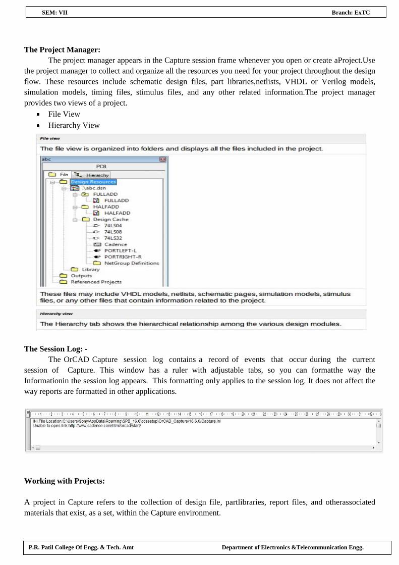
The Project Manager:
The project manager appears in the Capture session frame whenever you open or create aProject.Use
the project manager to collect and organize all the resources you need for your project throughout the design
flow. These resources include schematic design files, part libraries,netlists, VHDL or Verilog models,
simulation models, timing files, stimulus files, and any other related information.The project manager
provides two views of a project.
File View
Hierarchy View
The Session Log: -
The OrCAD Capture session log contains a record of events that occur during the current
session of Capture. This window has a ruler with adjustable tabs, so you can formatthe way the
Informationin the session log appears. This formatting only applies to the session log. It does not affect the
way reports are formatted in other applications.
Working with Projects:
A project in Capture refers to the collection of design file, partlibraries, report files, and otherassociated
materials that exist, as a set, within the Capture environment.
P.R. Patil College Of Engg. & Tech. Amt Department of Electronics &Telecommunication Engg.
SEM: VII Branch: ExTC
In this section:
Creating a Project
Setting Project Preferences
Setting up the Design Template
Dragging and dropping Folders, Pages and Parts
Capture Directory Map
Opening a project
Saving a project ,design or library
Closing a Project
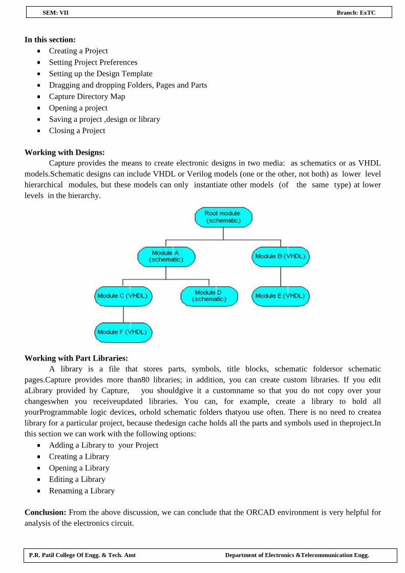
Working with Designs:
Capture provides the means to create electronic designs in two media: as schematics or as VHDL
models.Schematic designs can include VHDL or Verilog models (one or the other, not both) as lower level
hierarchical modules, but these models can only instantiate other models (of the same type) at lower
levels in the hierarchy.
Working with Part Libraries:
A library is a file that stores parts, symbols, title blocks, schematic foldersor schematic
pages.Capture provides more than80 libraries; in addition, you can create custom libraries. If you edit
aLibrary provided by Capture, you shouldgive it a customname so that you do not copy over your
changeswhen you receiveupdated libraries. You can, for example, create a library to hold all
yourProgrammable logic devices, orhold schematic folders thatyou use often. There is no need to createa
library for a particular project, because thedesign cache holds all the parts and symbols used in theproject.In
this section we can work with the following options:
Adding a Library to your Project
Creating a Library
Opening a Library
Editing a Library
Renaming a Library
Conclusion: From the above discussion, we can conclude that the ORCAD environment is very helpful for
analysis of the electronics circuit.

P.R. Patil College Of Engg. & Tech. Amt Department of Electronics &Telecommunication Engg.
SEM: VII Branch: ExTC
P.R. Patil College of Engineering & Management, Amravati
Department of Electronics & Telecommunication Engineering
Subject-SIMULATION LAB
SEM:VII Branch: EXTC
Experiment No.2
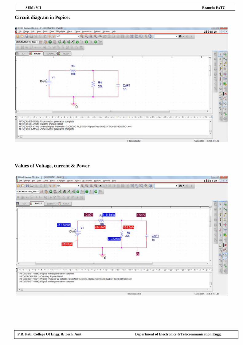
Aim: Tofindthe BIAS POINT Voltage, Current & Power of the given Network.
Facilities Required: -PC installed with CADENCE 16.6_OrCAD_Lite_All_Products.
Theory:
Biasing in electronics is the method of establishing predetermined voltages or currents at various
points of an electronic circuit for the purpose of establishing proper operating conditions in electronic
components. Many electronic devices whose function is processing time-varying (AC) signals also require a
steady (DC) current or voltage to operate correctly. The AC signal applied to them is superposed on this DC
bias current or voltage. Other types of devices, for example magnetic recording heads, require a time-
varying (AC) signal as bias. The operating point of a device, also known as bias point, quiescent point, or Q-
point, is the steady-state voltage or current at a specified terminal of an active device (a transistor or vacuum
tube) with no input signal applied
Procedure:
1) Open ORCAD Capture CIS Lite Software.
2) Go to File>New>Project>
3) Write the name of the project> Select the required .Lib file>
4) Click on projectname.dcn file> Schematic1> Page1 Double click on that >>
5) A new window will appear Go to place>pSpice Component> And place the required component>
6) Connect all the component>
7) Go to Pspice> New Simulation Profile>
8) Give the name to profile and new window of Simulation Setting will appear>
9) Make the changes with analysis type to use the bias point >
10) Go to Pspice > RUN>
11) Find the values of the VOLTAGE, CURREN & POWER..
12) Save and Run and generate the net list.
P.R. Patil College Of Engg. & Tech. Amt Department of Electronics &Telecommunication Engg.
SEM: VII Branch: ExTC
Circuit diagram in Pspice:
Values of Voltage, current & Power
P.R. Patil College Of Engg. & Tech. Amt Department of Electronics &Telecommunication Engg.
SEM: VII Branch: ExTC
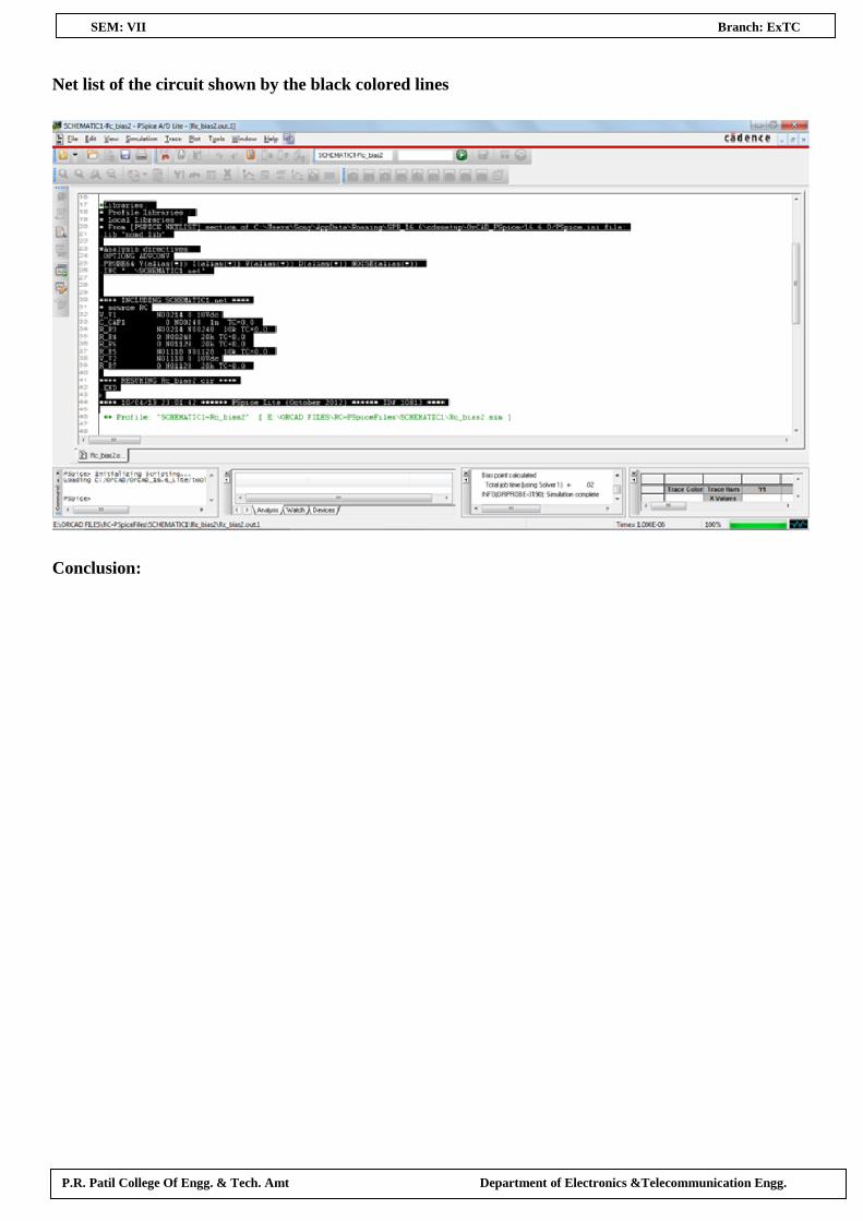
Net list of the circuit shown by the black colored lines
Conclusion:

P.R. Patil College Of Engg. & Tech. Amt Department of Electronics &Telecommunication Engg.
SEM: VII Branch: ExTC
P.R. Pote College of Engineering & Management, Amravati
Department of Electronics & Telecommunication Engineering
Subject-SIMULATION LAB
SEM: VII Branch: ExTC
Experiment No.3
Aim:To Observe the TIME DOMAIN (TRANSIENT) analysis of the simple RC Network.
Facilities Required: PC installed with CADENCE 16.6_OrCAD_Lite_All_Products.
Theory:
A change in the circuit operating conditions is the cause of a transient before reaching the steady
state operation which can be studied in the time domain by means of the set of the equations of the circuit
analysis. On‐off or off‐on mode changes of switches or sudden changes of the excitation (voltage or current
source modeled as step functions) are the cause of transients followed by a steady state operation that is the
response of the circuit to the changed condition. The transient response is the circuit’s temporary response
that will die out with time. This is the temporary part of the response. The transient response operation,
which will precede the establishment of the steady‐state operation, is due to the time required by the storage
elements to build the new conditions under which they will operate at the final steady‐state regime. The
storage elements may change their operation state with fulfilling the energy conservation principle. As a
consequence of it storage elements prevent instantaneous variation of energy in the transit from t = 0‐ to t =
0+.
Procedure:
1) Open ORCAD Capture CIS Lite Software>
2) Go to File>New>Project>
3) Write the name of the project> Select the required .Lib file>
4) Click on projectname.dcn file> Schematic1> Page1 Double click on that >>
5) A new window will appear Go to place>pSpice Component> And place the required component>
6) Connect all the component>
7) Go to Pspice> New Simulation Profile>
8) Give the name to profile and new window of Simulation Setting will appear>
9) Make the changes with analysis type to use the bias point >
10) Go to Pspice > RUN>
11) Find the values of the VOLTAGE, CURREN & POWER..
12) Save and Run and generate the net list.

P.R. Patil College Of Engg. & Tech. Amt Department of Electronics &Telecommunication Engg.
SEM: VII Branch: ExTC
Circuit diagram in Pspice:
Charging and discharging across the capacitor:

P.R. Patil College Of Engg. & Tech. Amt Department of Electronics &Telecommunication Engg.
SEM: VII Branch: ExTC
Net list of the circuit shown below:
Conclusion:

P.R. Patil College Of Engg. & Tech. Amt Department of Electronics &Telecommunication Engg.
SEM: VII Branch: ExTC
Experiment No.4
Aim:To Observe the AC Sweep/Noise analysis (dB Magnitude & Phase plot of the Voltage) of the given
RC Network.
Facilities Required: PC installed with CADENCE 16.6_OrCAD_Lite_All_Products.
Theory:
The topological analysis of basic ac electric circuits containing impedances and ideal ac supplies are
studied in AC analysis. Maximum power transfer theorems, Norton Theorem etc. are used for AC circuit
analysis.It is used for small signal analysis of circuits with sources of varying frequencies. It also calculates
all nodal voltages and branch currents (over a range of frequencies) and their magnitudes and phase angles.
The AC small-signal portion of Spice computes the AC output variables as a function of frequency. The
resultant linear circuit is analyzed over a user-specified range of frequencies. The desired output of an AC
small- signal analysis is usually a transfer function (voltage gain, trans-impedance, etc.). If the circuit has
only one AC input, it is convenient to set that input to unity and zero phases, so that output variables have
the same value as the transfer function of the output variable with respect to the input.
Procedure:
1) Open ORCAD Capture CIS Lite Software>
2) Go to File>New>Project>
3) Write the name of the project> Select the required .Lib file>
4) Click on projectname.dcn file> Schematic1> Page1 Double click on that >>
5) A new window will appear Go to place>pSpice Component> And place the required component>
6) Connect all the component>
7) Go to Pspice> New Simulation Profile>
8) Give the name to profile and new window of Simulation Setting will appear>
9) Make the changes with analysis type to use the bias point >
10) Go to Pspice > RUN>
11) Find the values of the VOLTAGE, CURREN & POWER..
12) Save and Run and generate the net list.

P.R. Patil College Of Engg. & Tech. Amt Department of Electronics &Telecommunication Engg.
SEM: VII Branch: ExTC
Circuit diagram in Pspice
dB Magnitude & Phase of Voltage:

P.R. Patil College Of Engg. & Tech. Amt Department of Electronics &Telecommunication Engg.
SEM: VII Branch: ExTC
Net list of the circuit shown below:
Conclusion:
P.R. Patil College Of Engg. & Tech. Amt Department of Electronics &Telecommunication Engg.
SEM: VII Branch: ExTC
Experiment No.5
Aim:To Observe the Charging & Discharging properties of series resistor, Capacitor & Inductor circuit with
Time Domain (Transient) Analysis that produces the waveform after initial charged values.
Facilities Required: PC installed with CADENCE 16.6_OrCAD_Lite_All_Products.
Theory:
The series RLC circuit above has a single loop with the instantaneous current flowing through the
loop being the same for each circuit element. Since the inductive and capacitive reactance's are a function of
frequency, the sinusoidal response of a series RLC circuit will vary with the applied frequency, (ƒ).
Therefore the individual voltage drops across each circuit element of R, L and C element will be "out-of-
phase" with each other. The phasor diagram for a series RLC circuit is produced by combining together the
three individual phasors above and adding these voltages vectorially. Since the current flowing through the
circuit is common to all three circuit elements we can use this as the reference vector with the three voltage
vectors drawn relative to this at their corresponding angles. The resulting vector VS is obtained by adding
together two of the vectors, VL and VC and then adding this sum to the remaining vector VR. The resulting
angle obtained between VS and I will be the circuits phase angle as shown below.
The amplitude of the source voltage is proportional to the amplitude of the current flowing through the
circuit. This proportionality constant is called the Impedance of the circuit which ultimately depends upon
the resistance and the inductive and capacitive reactance’s. Then in the series RLC circuit above, it can be
seen that the opposition to current flow is made up of three components, XL, XC and R with the reactance,
XT of any series RLC circuit being defined as: XT = XL - XC or XT = XC - XL with the total impedance of the
circuit being thought of as the voltage source required to drive a current through it.
Procedure:
1) Open ORCAD Capture CIS Lite Software>
2) Go to File>New>Project>
3) Write the name of the project> Select the required .Lib file>
4) Click on projectname.dcn file> Schematic1> Page1 Double click on that >>
5) A new window will appear Go to place>pSpice Component> And place the required component>
6) Connect all the component>
7) Go to Pspice> New Simulation Profile>
8) Give the name to profile and new window of Simulation Setting will appear>
9) Make the changes with analysis type to use the bias point >
P.R. Patil College Of Engg. & Tech. Amt Department of Electronics &Telecommunication Engg.
SEM: VII Branch: ExTC
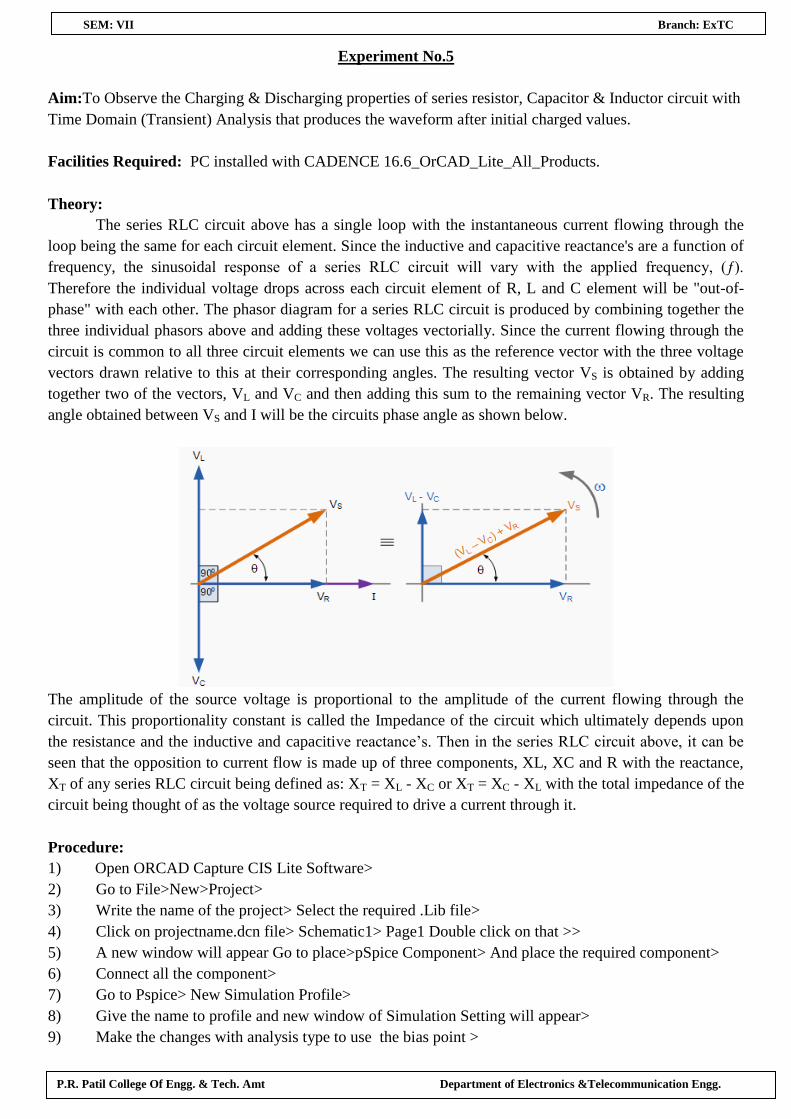
Circuit diagram formed:
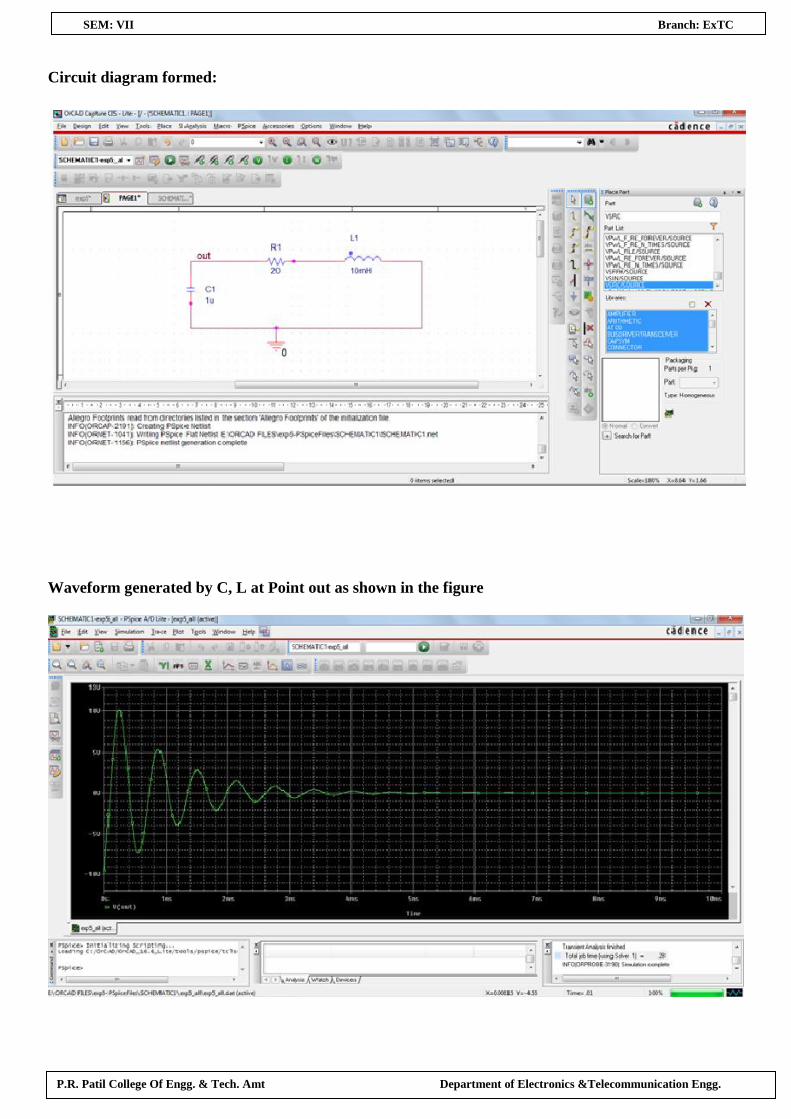
Waveform generated by C, L at Point out as shown in the figure

P.R. Patil College Of Engg. & Tech. Amt Department of Electronics &Telecommunication Engg.
SEM: VII Branch: ExTC
Net list of the circuit shown below:
Conclusion:
P.R. Patil College Of Engg. & Tech. Amt Department of Electronics &Telecommunication Engg.
SEM: VII Branch: ExTC
Experiment No.6
Aim:To Design and Simulate D-flip flop and D Latch in Simulink.
Facilities Required: PC installed with MATLAB and SIMULINK.
Theory:
Latches and flip-flops are the basic elements for storing information. One latch or flip-flop can store
one bit of information. The main difference between latches and flip-flops is that, for latches their outputs
are constantly affected by their inputs as long as the enable signal is asserted. In other words, when they are
enabled, their content changes immediately when their inputs change. Flip-flops, on the other hand, have
their content change only either at the rising or falling edge of the enable signal. This enable signal is usually
the controlling clock signal. After the rising or falling edge of the clock, the flip-flop content remains
constant even if the input changes.
There are basically four main types of latches and flip-flops: SR, D, JK, and T.The major differences
in these flip-flop types are the number of inputs they have and how they change state. For each type, there
are also different variations that enhance their operations.
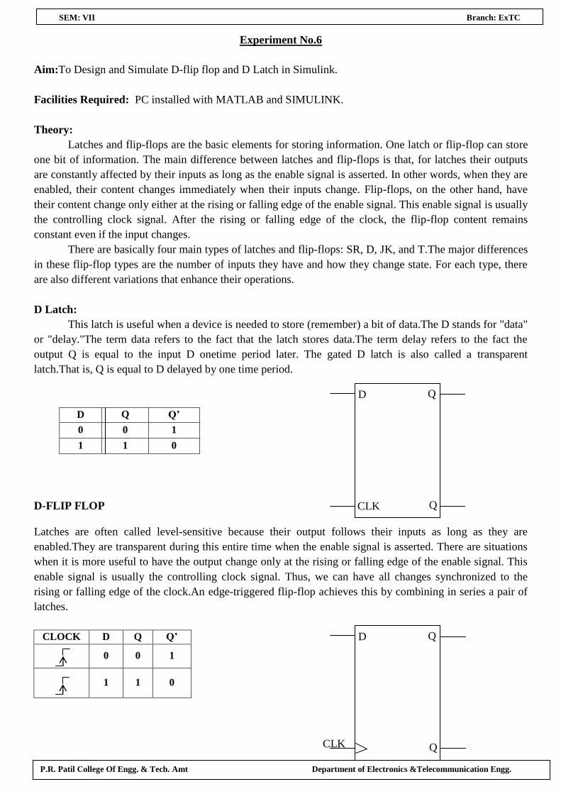
D Latch:
This latch is useful when a device is needed to store (remember) a bit of data.The D stands for "data"
or "delay."The term data refers to the fact that the latch stores data.The term delay refers to the fact the
output Q is equal to the input D onetime period later. The gated D latch is also called a transparent
latch.That is, Q is equal to D delayed by one time period.
D Q Q’
0 0 1
1 1 0
D-FLIP FLOP
Latches are often called level-sensitive because their output follows their inputs as long as they are
enabled.They are transparent during this entire time when the enable signal is asserted. There are situations
when it is more useful to have the output change only at the rising or falling edge of the enable signal. This
enable signal is usually the controlling clock signal. Thus, we can have all changes synchronized to the
rising or falling edge of the clock.An edge-triggered flip-flop achieves this by combining in series a pair of
latches.
CLOCK D Q Q’
0 0 1
1 1 0
D
CLK
Q
Q
´’
”’
”’
CLK
D Q
Q
´’
”’
”’
P.R. Patil College Of Engg. & Tech. Amt Department of Electronics &Telecommunication Engg.
SEM: VII Branch: ExTC
Procedure:
1. Open Matlab and then Simulink.
2. Create new model >Ctrl+N
3. Simulink> Sources> Constant.
4. Simulink> Sink> Scope.
5. Simulink Extras> Flip Flop> D Flip flop
6. Simulink Extras> Clock
7. Make connection as per logic diagram.
8. Simulate given circuit and observe output in Scope.
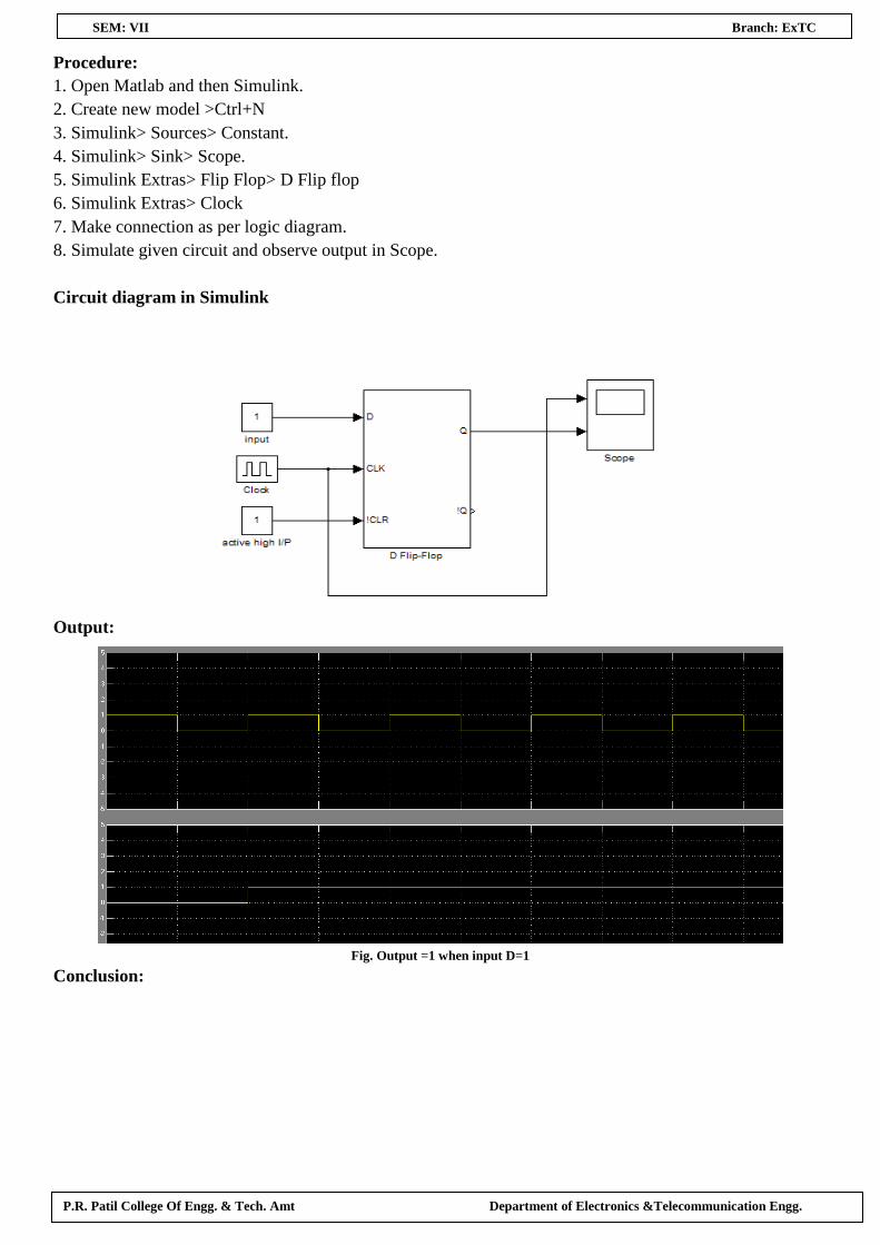
Circuit diagram in Simulink
Output:
Fig. Output =1 when input D=1
Conclusion:

P.R. Patil College Of Engg. & Tech. Amt Department of Electronics &Telecommunication Engg.
SEM: VII Branch: ExTC
Experiment No.7
Aim:To Design and Simulate MUX and DeMux as subsystem in Simulink.
Facilities Required: PC installed with MATLAB and SIMULINK.
Theory:
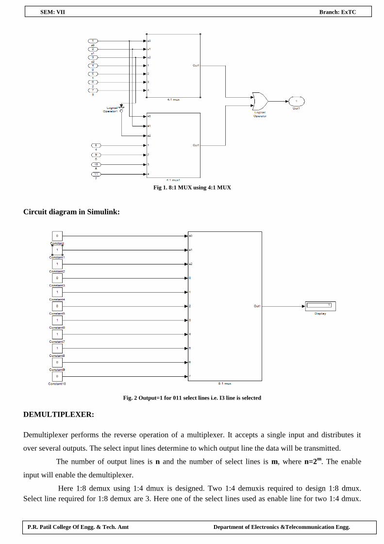
Multiplexer is a combinational logic circuit with multiple inputs and a single output.A multiplexer
(or mux) is a device that selects one of several analog or digitalinput signals and forwards the selected input
into a single line. A multiplexer of 2n inputs has n select lines, which are used to select which input line to
send to the output. Multiplexers are mainly used to increase the amount of data that can be sent over the
network within a certain amount of time and bandwidth. A multiplexer is also called a data selector. Where,
n=2m
. Consider 8 inputs MUX therefore; the select input required will be 23=8 where, n=8 and m=3
TRUTH TABLE:
INPUT SELECT LINE OUTPUT
I S2 S1 S0 Y
I0 0 0 0 D0
I1 0 0 1 D1
I2 0 1 0 D2
I3 0 1 1 D3
I4 1 0 0 D4
I5 1 0 1 D5
I6 1 1 0 D6
I7 1 1 1 D7
LOGIC DIAGRAM:
P.R. Patil College Of Engg. & Tech. Amt Department of Electronics &Telecommunication Engg.
SEM: VII Branch: ExTC
Fig 1. 8:1 MUX using 4:1 MUX
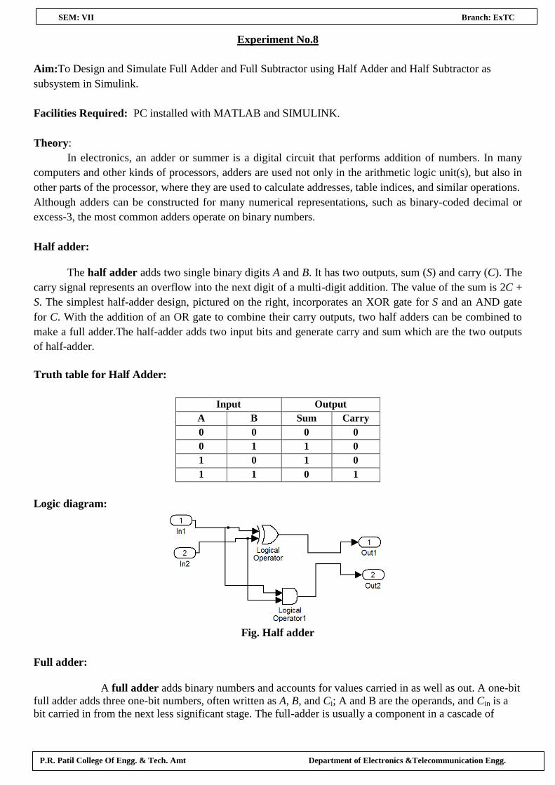
Circuit diagram in Simulink:
Fig. 2 Output=1 for 011 select lines i.e. I3 line is selected
DEMULTIPLEXER:
Demultiplexer performs the reverse operation of a multiplexer. It accepts a single input and distributes it
over several outputs. The select input lines determine to which output line the data will be transmitted.
The number of output lines is n and the number of select lines is m, where n=2m
. The enable
input will enable the demultiplexer.
Here 1:8 demux using 1:4 dmux is designed. Two 1:4 demuxis required to design 1:8 dmux.
Select line required for 1:8 demux are 3. Here one of the select lines used as enable line for two 1:4 dmux.

P.R. Patil College Of Engg. & Tech. Amt Department of Electronics &Telecommunication Engg.
SEM: VII Branch: ExTC
1:8 demux having only 1 input and 8 output lines. There is common data connected to both demux. Select
lines are ‘a’, ’b’, ’c’. Select line ‘a’ is connected directly to enable second 1:4 demux whereas inverted ‘a’ is
connected to enable first 1:4 demux.
TRUTH TABLE:
INPUT SELECT LINE OUTPUT
D
S2 S1 S0 Y
0 0 0 D0
0 0 1 D1
0 1 0 D2
0 1 1 D3
1 0 0 D4
1 0 1 D5
1 1 0 D6
1 1 1 D7
LOGIC DIAGRAM:

P.R. Patil College Of Engg. & Tech. Amt Department of Electronics &Telecommunication Engg.
SEM: VII Branch: ExTC
1:8 DeMux using 4:1 DeMUX
Fig. 1:8 demux using 1:4 demux
Circuit diagram in Simulink:
Conclusion:
P.R. Patil College Of Engg. & Tech. Amt Department of Electronics &Telecommunication Engg.
SEM: VII Branch: ExTC
Experiment No.8
Aim:To Design and Simulate Full Adder and Full Subtractor using Half Adder and Half Subtractor as
subsystem in Simulink.
Facilities Required: PC installed with MATLAB and SIMULINK.
Theory:
In electronics, an adder or summer is a digital circuit that performs addition of numbers. In many
computers and other kinds of processors, adders are used not only in the arithmetic logic unit(s), but also in
other parts of the processor, where they are used to calculate addresses, table indices, and similar operations.
Although adders can be constructed for many numerical representations, such as binary-coded decimal or
excess-3, the most common adders operate on binary numbers.
Half adder:
The half adder adds two single binary digits A and B. It has two outputs, sum (S) and carry (C). The
carry signal represents an overflow into the next digit of a multi-digit addition. The value of the sum is 2C +
S. The simplest half-adder design, pictured on the right, incorporates an XOR gate for S and an AND gate
for C. With the addition of an OR gate to combine their carry outputs, two half adders can be combined to
make a full adder.The half-adder adds two input bits and generate carry and sum which are the two outputs
of half-adder.
Truth table for Half Adder:
Input Output
A B Sum Carry
0 0 0 0
0 1 1 0
1 0 1 0
1 1 0 1
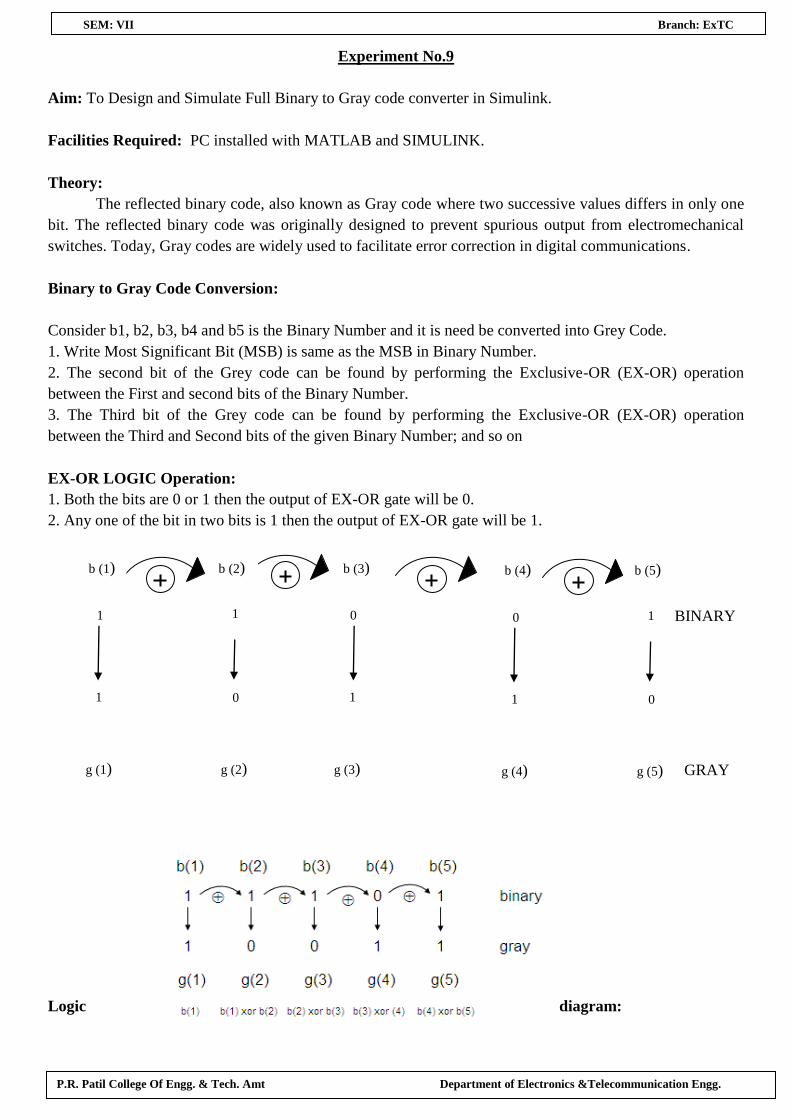
Logic diagram:
Fig. Half adder
Full adder:
A full adder adds binary numbers and accounts for values carried in as well as out. A one-bit
full adder adds three one-bit numbers, often written as A, B, and Ci; A and B are the operands, and Cin is a
bit carried in from the next less significant stage. The full-adder is usually a component in a cascade of

P.R. Patil College Of Engg. & Tech. Amt Department of Electronics &Telecommunication Engg.
SEM: VII Branch: ExTC
adders, which add 8, 16, 32, etc. bit wide binary numbers. The circuit produces a two-bit output, output
carry and sum typically represented by Cout and S where sum = 2x Cout+ S.
Truth table for Full Adder:
Inputs Output
A B Ci Sum Carry
0 0 0 0 0
0 0 1 1 0
0 1 0 1 0
0 1 1 0 1
1 0 0 1 0
1 0 1 0 1
1 1 0 0 1
1 1 1 1 1
Logic diagram:
Fig. Full Adder
Circuit diagram for Full adder using Half adder:
Fig. full adder using half adder
Conclusion:
P.R. Patil College Of Engg. & Tech. Amt Department of Electronics &Telecommunication Engg.
SEM: VII Branch: ExTC
Experiment No.9
Aim: To Design and Simulate Full Binary to Gray code converter in Simulink.
Facilities Required: PC installed with MATLAB and SIMULINK.
Theory:
The reflected binary code, also known as Gray code where two successive values differs in only one
bit. The reflected binary code was originally designed to prevent spurious output from electromechanical
switches. Today, Gray codes are widely used to facilitate error correction in digital communications.
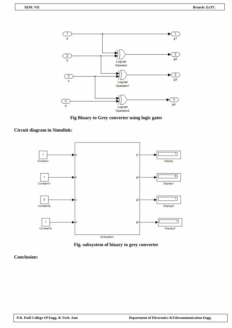
Binary to Gray Code Conversion:
Consider b1, b2, b3, b4 and b5 is the Binary Number and it is need be converted into Grey Code.
1. Write Most Significant Bit (MSB) is same as the MSB in Binary Number.
2. The second bit of the Grey code can be found by performing the Exclusive-OR (EX-OR) operation
between the First and second bits of the Binary Number.
3. The Third bit of the Grey code can be found by performing the Exclusive-OR (EX-OR) operation
between the Third and Second bits of the given Binary Number; and so on
EX-OR LOGIC Operation:
1. Both the bits are 0 or 1 then the output of EX-OR gate will be 0.
2. Any one of the bit in two bits is 1 then the output of EX-OR gate will be 1.
Logic diagram:
b (3)
0
1
g (3)
b (4) b (5)
0
1
g (4)
1
0
g (5)
b (1) b (2)
1
1
g (1)
1
0
g (2) GRAY
BINARY
P.R. Patil College Of Engg. & Tech. Amt Department of Electronics &Telecommunication Engg.
SEM: VII Branch: ExTC
Fig Binary to Grey converter using logic gates
Circuit diagram in Simulink:
Fig. subsystem of binary to grey converter
Conclusion:

P.R. Patil College Of Engg. & Tech. Amt Department of Electronics &Telecommunication Engg.
SEM: VII Branch: ExTC
Experiment No.10
Aim: To Design and Simulate sequence generator to generate a given sequence as 1,3,4,7.
Facilities Required: PC installed with MATLAB and SIMULINK.
Theory:
The circuit which generates the desired sequence of bits is known as sequence generator. Sequence
generator is categorized into two types as follows:
1. Synchronous sequence generator.
2. Asynchronous sequence generator.
In synchronous mode same clock is applied to all flip-flop is known as synchronous sequence
generator. We have to generate a sequence 1,3,4,7 using synchronous clock mode.
Truth table for sequence generator:
PRESENT STATE NEXT STATE FLIP FLOP INPUTS
QB QC QD QB QC QD JB KB JC KC JD KD
0 0 1 0 1 1 0 X 1 X X 0
0 1 1 1 0 0 1 X X 1 X 1
1 0 0 1 1 1 X 0 1 X 1 X
1 1 1 0 0 1 X 1 X 1 X 0
0 0 0 0 0 1 0 X 0 X 1 X
0 1 0 0 1 1 0 X X 0 1 X
1 0 1 1 1 1 X 0 1 X X 0
1 1 0 1 1 1 X 0 X 0 1 X
K – Map Equations:
JB = KB = QCQD
JC = QD + QB
KC = QD
JD = 1
KD = QBQC
Circuit diagram in Simulink:
P.R. Patil College Of Engg. & Tech. Amt Department of Electronics &Telecommunication Engg.
SEM: VII Branch: ExTC
Output:
Conclusion:

P.R. Patil College Of Engg. & Tech. Amt Department of Electronics &Telecommunication Engg.
SEM: VII Branch: ExTC
Experiment No.11
Aim: To Design and Simulate Up-down counter.
Facilities Required: PC installed with MATLAB and SIMULINK.
Theory:
The UP/DOWN counter in increasing or decreasing direction as per the control inputs .Whenever
the circuit is designed to operate for more than one operation, the control input are provided to control the
operation . Let’s consider UP/DOWN is a control inputs, which controls the direction of the counter. When
UP/DOWN input is 0,the direction of the counter is in decreasing direction and counter is said to be Down
Counter, When UP/DOWN input is 1, then the direction of counter is in increasing direction and counter is
said to be an Up Counter.
Here we design counter using J-K flip flop with the help of MATLAB 7.10 software.
Circuit diagram in Simulink:
P.R. Patil College Of Engg. & Tech. Amt Department of Electronics &Telecommunication Engg.
SEM: VII Branch: ExTC
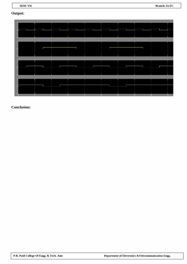
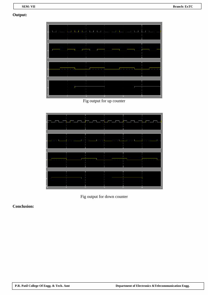
Output:
Fig output for up counter
Fig output for down counter
Conclusion:
P.R. Patil College Of Engg. & Tech. Amt Department of Electronics &Telecommunication Engg.
SEM: VII Branch: ExTC
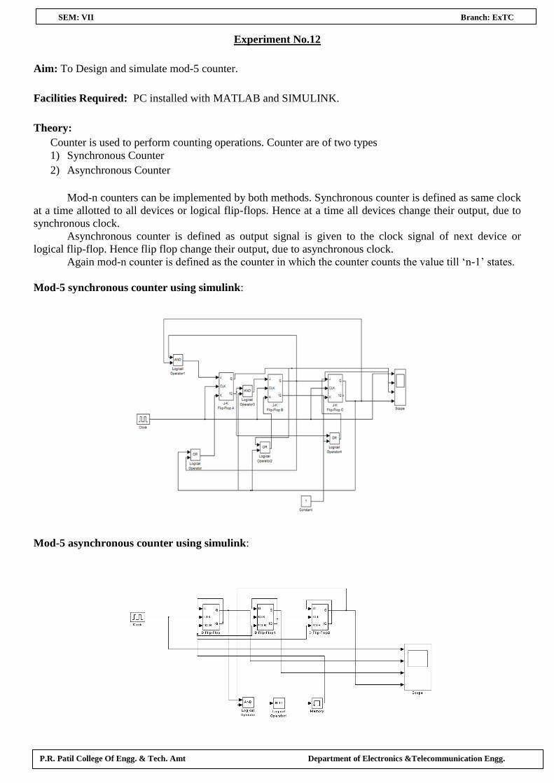
Experiment No.12
Aim: To Design and simulate mod-5 counter.
Facilities Required: PC installed with MATLAB and SIMULINK.
Theory:
Counter is used to perform counting operations. Counter are of two types
1) Synchronous Counter
2) Asynchronous Counter
Mod-n counters can be implemented by both methods. Synchronous counter is defined as same clock
at a time allotted to all devices or logical flip-flops. Hence at a time all devices change their output, due to
synchronous clock.
Asynchronous counter is defined as output signal is given to the clock signal of next device or
logical flip-flop. Hence flip flop change their output, due to asynchronous clock.
Again mod-n counter is defined as the counter in which the counter counts the value till ‘n-1’ states.
Mod-5 synchronous counter using simulink:
Mod-5 asynchronous counter using simulink:

P.R. Patil College Of Engg. & Tech. Amt Department of Electronics &Telecommunication Engg.
SEM: VII Branch: ExTC
Output:
For synchronous counter:
For asynchronous counter:
Conclusion:

P.R. Patil College Of Engg. & Tech. Amt Department of Electronics &Telecommunication Engg.
SEM: VII Branch: ExTC
Experiment No.13
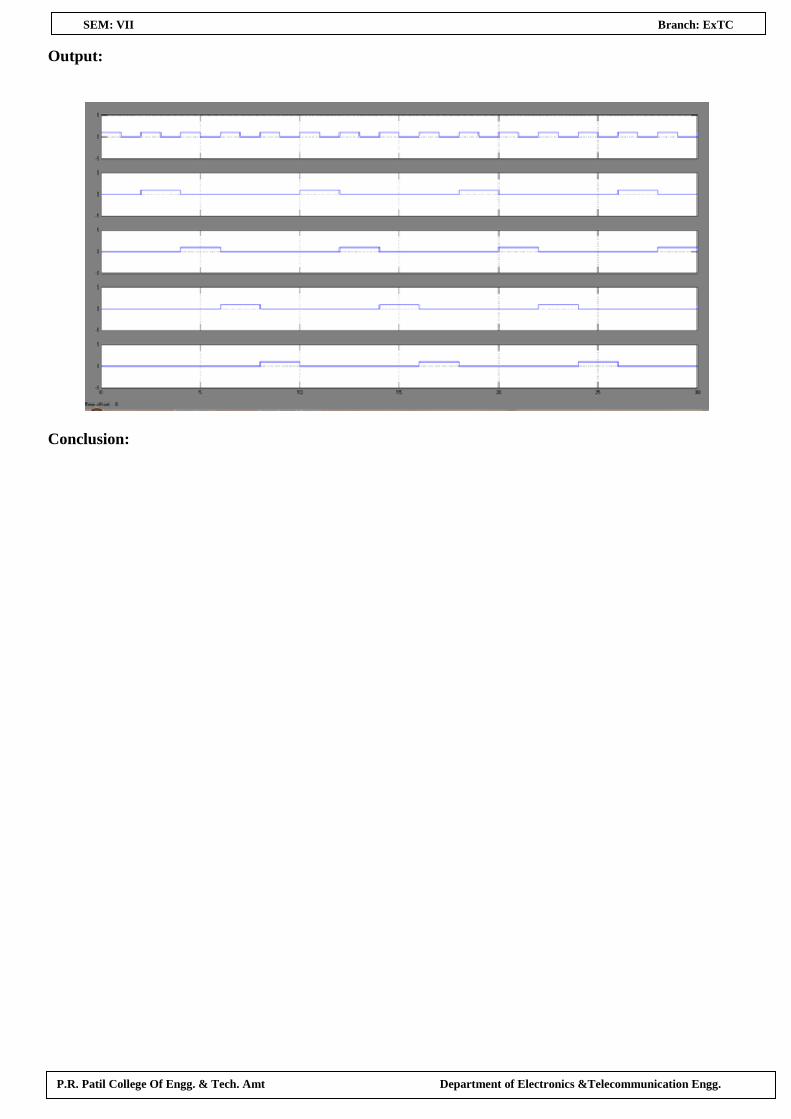
Aim: To Design and simulate 4 bit Johnson Counter.
Facilities Required: PC installed with MATLAB and SIMULINK.
Theory:
In Johnson counter, the Q output of each stage of flip flop is connected to the J input of next stage.
The single exception is that the output of last flip flop is cross coupled with the input of first flip flop. There
is a feedback from rightmost flip flop compliment output to the leftmost flip flop J input. This arrangement
produces a unique sequence of states.
Initially, the register (all flip flops) is cleared. So all the outputs, Qa, Qb, Qc, Qd are zero. The output
of last stage, Qd is zero. Therefore compliment output of last stage, Qd is one. This is connected back to J
input of first stage, and the output which is Qd is zero is connected to input K of first flip flop.
Truth Table:
CLOCK
PULSE
Qa Qb Qc Qd
0 0 0 0 0
1 1 0 0 0
2 1 1 0 0
3 1 1 1 0
4 1 1 1 1
5 0 1 1 1
6 0 0 1 1
7 0 0 0 1
Circuit diagram in simulink:
Scope
J-K
Flip -Flop 3
J
CLK
K
Q
!Q
J-K
Flip -Flop 2
J
CLK
K
Q
!Q
J-K
Flip -Flop 1
J
CLK
K
Q
!Q
J-K
Flip -Flop
J
CLK
K
Q
!Q
Clock

P.R. Patil College Of Engg. & Tech. Amt Department of Electronics &Telecommunication Engg.
SEM: VII Branch: ExTC
Output:
Conclusion:
P.R. Patil College Of Engg. & Tech. Amt Department of Electronics &Telecommunication Engg.
SEM: VII Branch: ExTC
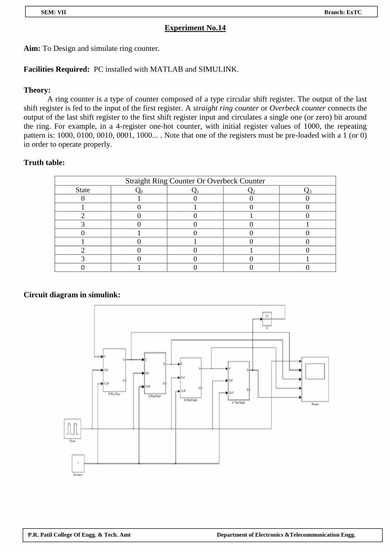
Experiment No.14
Aim: To Design and simulate ring counter.
Facilities Required: PC installed with MATLAB and SIMULINK.
Theory:
A ring counter is a type of counter composed of a type circular shift register. The output of the last
shift register is fed to the input of the first register. A straight ring counter or Overbeck counter connects the
output of the last shift register to the first shift register input and circulates a single one (or zero) bit around
the ring. For example, in a 4-register one-hot counter, with initial register values of 1000, the repeating
pattern is: 1000, 0100, 0010, 0001, 1000... . Note that one of the registers must be pre-loaded with a 1 (or 0)
in order to operate properly.
Truth table:
Straight Ring Counter Or Overbeck Counter State Q0 Q1 Q2 Q3
0 1 0 0 0
1 0 1 0 0
2 0 0 1 0
3 0 0 0 1
0 1 0 0 0
1 0 1 0 0
2 0 0 1 0
3 0 0 0 1
0 1 0 0 0
Circuit diagram in simulink:
P.R. Patil College Of Engg. & Tech. Amt Department of Electronics &Telecommunication Engg.
SEM: VII Branch: ExTC
Output:
Conclusion: