Simulation of Wire Antennas using 4NEC2 - qsl.net · 1 Simulation of Wire Antennas using 4NEC2 A...
42
1 Simulation of Wire Antennas using 4NEC2 A Tutorial for Beginners Version 1.0 Author: Gunthard Kraus, Oberstudienrat, Elektronikschule Tettnang, Germany Email: [email protected] Consultant: Hardy Lau, Dipl.-Eng. (DH) Duale Hochschule Baden Württemberg (DHBW), Friedrichshafen, Germany August 15th, 2010
Transcript of Simulation of Wire Antennas using 4NEC2 - qsl.net · 1 Simulation of Wire Antennas using 4NEC2 A...

1
Simulation of Wire Antennas using 4NEC2
A Tutorial for Beginners
Version 1.0 Author: Gunthard Kraus , Oberstudienrat, Elektronikschule Tettnang, Germany Email: [email protected] Consultant: Hardy Lau , Dipl.-Eng. (DH) Duale Hochschule Baden Württemberg (DHBW), Friedrichshafen, Germany
August 15th, 2010

2
Content Page 1. Introduction 3 2. Installation 3 3. Getting Started 3 4. Geometry Builder, Geometry Editor or Text Editor to create an NEC File 4 5. Start with the included „example2.nec“ (300MHz D ipole) 5
5.1. Far Field Simulation 5 5.2. Coloured 3D Presentation 7 5.3. Opening the NEC File with Notepad 10 5.4. Using the 4NEC2 Editor 12
5.4.1. Working with the old 4NEC2 editor 12 5.4.2. The new 4NEC2 editor 12
5.5. Near Field Simulation 14 5.6. Sweeping the SWR and the Input Reflection 15 6. First own Project: 300MHz Dipole over realistic Ground 16
6.1. Modification of the NEC-File 1 6 6.2. Far Field Simulation 18 6.3. Near Field Simulation 19 6.4. Sweeping the SWR and the Input Reflection 20
7. Second Project: 300MHz Dipole using thick Wires 21
7.1. The thick wire problem 21 7.2. Far Field and Near Field Simulation 22 7.3. Sweeping the SWR and the Input Reflection 22 7.4. Sweeping the Antenna Gain 23
7.5. Sweeping the Input Impedance 24 8. A wonderful toy: the Smith Chart Machine 25 9. Optimizing (Key F12) 27 9.1. Optimizing the Antenna Length (thick wire dipo le of chapter 7) 27 9.2. Parameter Sweep 29 9.2.1. Input Impedance for different Antenna Heights 29 9.2.2. Far Field Pattern for different Antenna Heights 31 10. Third Project: Geometry Builder or Text Editor to design a Helix Antenna? 32 10.1. Fundamentals of Helix Antenna Design 32 10.2. Design using the Geometry Builder 33
10.3. Far Field Simulation 34 10.4. Frequency Sweep of Gain and Impedance 34 10.5. Once more the same procedure, but now using t he Notepad Editor 35 10.6. Once more: Far Field Simulation 37 10.7. Once more: Frequency Sweep of Gain and Impeda nce 38 10.8. Feeding the Antenna by a short piece of wire 38
Appendix: A short Overview of the most important NEC Cards 41

3
1. Introduction NEC (= Numerical Electric Code ) is a simulation method for wire antennas, developed by the Lawrence Livermore Laboratory in 1981 or the Navy. To realize this an antenna is divided into “short segments” with linear variation of current and voltage (like SPICE when simulating circuits). The results are very convenient and the standard for this simulation technique is NEC2. Time is running and so the weaknesses of NEC2 (e. g. simulation errors when wires are crossing in a very short distance or when using buried wires) were overcome with 4NEC2. But 4NEC2 was top secret for a long time, no export allowed and still today very expensive (= starting at 2000$). So a normal private user will take NEC2 and has the choice between lots of offers in the Internet. The two leaders are EZNEC (= not free of charge) and 4NEC2 (= completely free). Especially 4NEC2 offers a huge amount of possibilities and options (including graphical 3D display of the results) and was programmed by Arie Voors. Its main advantages are the optimizing tools and the parameter sweeps. It can be found and downloaded free of charge from the Internet. Two program packages must be installed: first „4NEC2.zip“ and afterwards „4NEC2X.zip“ in the same directory. „4NEC2“ is the NEc calculator but „4NEC2X“ (= 4NEC2 Ext ended) offers after pressing F9 the mentioned coloured 3D presentation of the simulation results with a lot of features . Please note: 4NEC2 is an unbelievable huge tool with infinite pos sibilities. So this tutorial wants to “open a door” and so the user gets the necessary fundamental informat ion about the usage of the software. He has then to continue itself…. 2. Installation No problem: after the download (http://home.ict.nl/~arivoors/) unzip the package and start the 4NEC2 exe file. After the successful installation right click on the 4NEC2X – exe file and install this software in the same directory. The software is completely free and no licensing necessary. Bugs or proposals for improvements can be mailed to the author Arie Voors who has done a huge work. So tell him „Thank you“ in the mail for his work.
3. Getting Started Click on the 4NEC2X icon and you get two windows on your screen: Main (F2) and Geometry (F3) After the simulation two additional windows can be opened: Pattern (F4) and Impedance / SWR / Gain (F5) . : Remarks:
a) Input and property inputs, modifications and start of simulation are all done in the Main window. b) The antenna geometry is shown in the Geometry window due to the Input NEC File.
c) Far field and near field simulation results are presented in the Pattern window.
d) And finally when sweeping you can see the impedance or the SWR or the F/B ratio versus frequency by
pressing F5.

4
4. Geometry Builder, Geometry Editor or Text Editor to create a NEC File? This must be decided by the user who has the choice. a) Creating the NEC file with the Geometry Builder is fine. For Patch-, Plane-, Box-, Helix-, Spherical-, Cylinder- or Parabolic structures there exist own menus with own screens and the usage is really simple. But you have only the listed 7 antenna types… b) To create any desired structure is an affair for the Geometry Editor . This editor this mainly foreseen for beginners and is easy of use. The next 3 editors concentrate directly on the NEC file, because this is the goal of all preparation for the simulation. That needs more effort for the user but gives more options for simulation and optimizing. But remember: All length values in a NEC File are always read as „ Meters“. Otherwise you must write an additional “GS” card with a scaling factor for correction (example: entries in Inches…) which is applied to the comple te structure. But now let’s have a look at the 3 editors: With a simple text editor like Notepad you have to write the pure NEC file and / or modify entries in it. So the complete antenna structure must exist in your brain before writing -- but this is the fastest and most effective way. That is not difficult and after a short time you ar e familiar with this method. Then you are able to m odify structures or parts of them in a hurry…. The „old 4NEC2 – Editor“ was a progress because of using buttons to separate the different parts of the NEC file (but today no longer used and maintained). e) the „new 4NEC2-Editor“ uses menus with lines and columns for the different entries. Very fine -- but the user with lot of experience misses now the direct view on the complete NEC file. So after some time of working with 4NEC2 nearly everybody returns to Notepad..... In the following examples and projects all these different editor methods are demonstrated. So please examine and decide yourself.

5
5. Starting with the included “example2.nec“ (300MH z Dipole)
5.1. Far Field Simulation Please change to the folder “models “ and open the “example2.nec” file.
In the left (= Main) window you find the simulation frequency and wavelength (= big red circle). The small red circle in the under left corner of the window indicates that the dipole is divided into 9 segments. The right window shows the dipole geometry in the related coordinate system.
Now press the F7 button (= start of calculation) and choose „Far Field pattern “, “Full “ and “Generate “. An arc resolution of 5 degrees will do the job for the first time, giving short calculating times. Then press “Generate”.

6
This is the success and the main window is now fulfilled with entries and data. Now Press F4 and the vertical radiation pattern is shown in an additional window.
The „Show “ menu in the Pattern (F4) window offers several options. With “Next pattern” and Previous pattern” you can walk through the diagrams.
Pressing „Indicator “ gives an additional radial cursor for the diagram. If you left click on any point of the pattern curve with the mouse the cursor snaps to this point and the values of this point are indicated.

7
Under “Far Field “ can be found:
a) The switch for changing to the Horizontal Plane.
b) The option to change to the „ARRL-style scale “, using a logarithmic scaling for the amplitude including an „automatic scaling spread“. So all lobes of a pattern are visible without efforts.
c) “Multi Pattern “ shows all diagrams for chosen
polarity.
d) “Bold lines “ gives thick lines of the curves and
e) “Font scaling “ is self explaining.
f) At last you can switch the azimuth angle (Phi) and / or the elevation angle (Theta) forward or reverse.
The rest of the menu should be tested by yourself.
5.2. Coloured 3D Presentation This option needs „4NEC2X“ . So please start your work in the future always by opening this program.
Close 4NEC2 and start 4NEC2X Use again the „example2.nec“ file and repeat the far field simulation. Then select F9 to start the 3D Viewer and you will get this screen. Now press the left mouse button when rolling your mouse -- this varies the azimuth and elevation angle of the diagram (…for you the result is like a flight in a helicopter around the antenna…).

8
Now play a little bit with the following buttons:
a) „Ident “ is used to identify and to mark a desired segment after entering the segment number. b) „Res“ = “Reset “ to the start position after the invoke of the 3D presentation.
c) “Rotc “ is used to define a segment as rotation centre.
d) „Col“ invokes the colour menu .
Let us continue with the proposed 3D presentation of the antenna’s radiation. Chose these settings…. …and you get this screen. The pattern can be rotated like before by using the mouse.
9
Here follow some presentations which are of interest for a lot users:
At first the current distribution on the antenna wire…
…or additionally the phase distribution.
Or all the segments of the wire can be made visible:
Play now yourself with this huge amount of possibilities…but this takes time….

10
5.3. Opening the NEC-File with Notepad Change to the Main menu (F2), open “settings” and chose notepad editor . Then press F6 to open the NEC file of the antenna. Please do not jump over this chapter, because a deep analysis of the NEC file details helps to modify or to optimize or to analyse error messages.
Every line starts with a short abbreviation (= card name) and describes in a short form the task of the line.
Attention: In the main window you find a “NEC short reference“ in the help menu. Now let us examine every line. Line 1 and line 2 : “CM“ starts a comment line with a maximum of 30 signs. ---------------------------------------------------------------------------------------------------------------------------------------- Line 3: “ CE“ is “End of comment “ ----------------------------------------------------------------------------------------------------------------------------------------- Line 4: “SY“ stands for a “Symbol“ and this is always a Variable (here: length = len=0.4836 ).
Caution: all length values in a NEC file are given a nd calculated in Meters. Corrections can be made by using an additional “GS” card (= geometry scaling) e. g. when using feet instead of meters. This scaling factor is applied to the complete structure.
--------------------------------------------------------------------------------------------------------------------------------------- Line 5: “ GW“ =„Geometry of wire“. Let us have a detailed look at the entries of this line. The line starts with “1“ (= “Wire number 1 “). “9“ indicates that the wire is divided into 9 Segments . “0 / -len/2 / 0“ are the xyz coordinates of the wire’s starting point . Length unit is
always “Meter“. “0 / len/2 / 0“ are the xyz coordinates of the wire’s end point . “.0001“ is the wire’s radius in Meters . ------------------------------------------------------------------------------------------------------------------------------------ Line 6: „GE“ = end of “geometry information “, followed by a number which describes the
ground “0“ means: no ground = free space.
“-1“ or “1“ represent a ground, but the details mus t be entered in a separate “Ground card“ (= GN card) .
------------------------------------------------------------------------------------------------------------------------------------

11
Line 7: „ LD“ = „Loading of a segment “. Please use the NEC short reference and the NEC manual in the online help to find out all options.
“5” = in this example only “LD 5“ is used to enter the conductivity of the antenna wire .
“1” = Wire 1 .
„0 0“ = two empty fields. „5.8001E7“ is the conductivity for copper ( in mhos). ---------------------------------------------------------------------------------------------------------- Line 8: “ EX“ = “Exitation “. “0“ = a voltage source is used for excitation. “1“ = wire 1 (= tag 1) is excited “5“ = excited segment of Wire 1. “0“ = an empty field. „1 0“ = real and imaginary part of the applied complex voltage (1 + j0). So in this case a real voltage of 1V is used ---------------------------------------------------------------------------------------------------------- Line 9: “ FR“ = frequency information.
Normally a sweep is used and must be programmed. So some information is necessary if only a fixed frequency is used:
“0“ = linear frequency sweep (“1“ gives a logarithmic sweep) “1“ = only one frequency step is foreseen. “0 0“ = two empty fields. “300“ = start value of frequency = 300MHz. “0“ = gives a frequency step width of Null MHz --------------------------------------------------------------------------------------------------------- Line 10: “ EN“ = end of NEC file ---------------------------------------------------------------------------------------------------------

12
5.4. Using the 4NEC2 Editor Caution: As already mentioned you have the choice between an old and a new version (…you find them in the “Settings” of the Main menu). 5.4.1. Working with the old 4NEC2 Editor No problem, it’s like working with Notepad in a modern environment. But this editor version is obsolete.
------------------------------------------------------------------------------------------------------------------------------------------------------- 5.4.2. The new 4NEC2 Editor
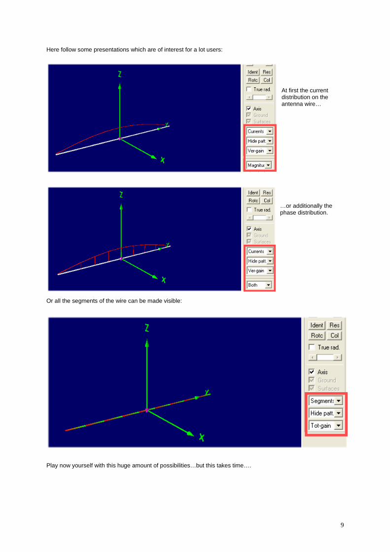
The editor can either be invoked by pressing <Control> + <F4> or by opening “Settings ” in the main menu followed by “Edit / Open Input NEC File”. This is the first card named “Symbols ”.
All the used wires and their properties are listed on the next card “Geometry “ (Tag Number / number of segments / xyz coordinates of wire start and end / radius of wire in Meters ).
13
--------------------------------------------------------------------------------------------- On the Source / Load card must be noted that a real voltage source (magnitude = 1V) is connected to Tag 1 / Segment 5 . (Remember: In the load card “LD” in the true NEC file there was only one entry the value of the conductivity of the
copper for the wire).

14
At last information about frequency and sweeping must be entered. No problem for a fixed frequency simulation at 300MHz and a dipole in free space.
----------------------------------------------------------------------------------------------------------------------------------------
5.5. Near Field Simulation
Open main “ (F2) and press “F7“. Then choose “Near Field Pattern “ and “E-Field “ and check the entries. This is the task: Show the E Field distribution for Y = 0 (= centre of dipole as seen in the direction of the antenna wire and step „X“ from -20m to +20m in steps of 1,6m and „Z“ from 0 to 50m in steps of 2m.“
This is the simulation result. Important: The scaling of the field distribution belongs to an Input Power of 100W (See the “Settings” menu and then „Input Power“ for changing) (Remember: This power value is also used when simulating the current distribution on the antenna wire).

15
5.6. Sweeping the SWR and the Input Reflection
Press F2, then „F7. Select “Frequency sweep “. Enter the sweep range from 295 to 305 MHz in the lower half of the menu. Use a step width of 0.1MHz. Select „Ver“ (= Vertical Pattern) and start the Simulation with the button “Generate “.
Simulation result:

16
6. First own Project: 300MHz Dipole over realistic Ground
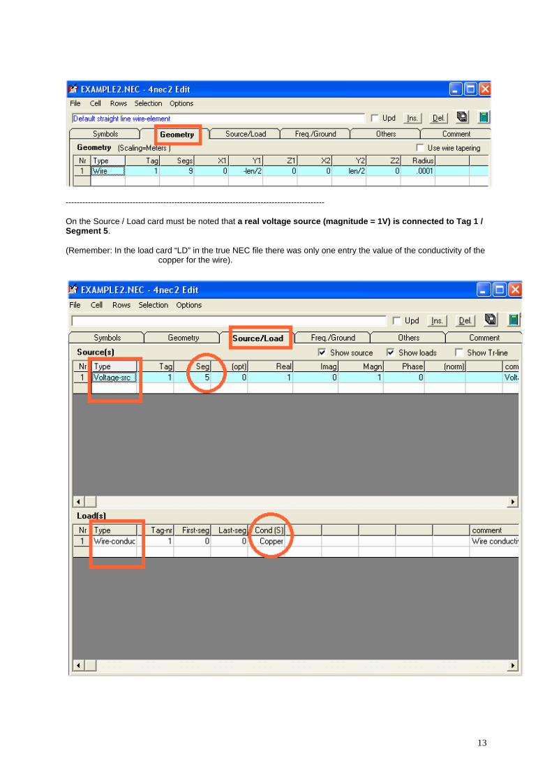
6.1. Modification of the NEC-File The easiest way is to use the NEC file of the last example and to modify it:
a) now the dipole hangs 1m above the ground and b) a realistic ground shall be used.
At first create a new folder for own projects (e. g. “own_examples “) and in it an additional folder this task (“dipole_over_ground “). Then copy the NEC file of the last example into this new folder and rename it to
dipole_over_ground.nec Then start 4NEC2X and select the new 4NEC2 editor in the settings menu. Open the new file “dipole_over_ground.nec” (by pressing F6). At first enter in the geometry card the height of the dipole’s start and end point to z = 1m
Then switch to “Freq./Ground”. Select “Real ground “ and “Average “. Let the field “Connect wire for Z = 0 to ground“ free.
Now open the NEC file with notepad to see the modifications:
17
The entries in the Ground card GN are easy to understand: „2“ = Sommerfeld Norton Ground. „13“ = Dielectric constant „.005“ = Conductivity in mhos/m
18
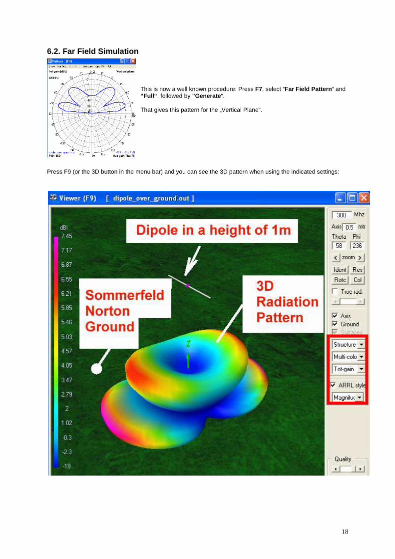
6.2. Far Field Simulation This is now a well known procedure: Press F7, select “Far Field Pattern “ and “Full“ , followed by ”Generate “. That gives this pattern for the „Vertical Plane“.
Press F9 (or the 3D button in the menu bar) and you can see the 3D pattern when using the indicated settings:

19
6.3. Near Field Simulation
No problem: use these settings and at once you get the Electrical Field Strength around the dipole. Input power is 100W.

20
6.4. Sweeping the SWR and the Input Reflection
Open this well known F7 menu, select “Frequency sweep “ and choose a sweep range from 295 to 305MHz with a frequency step of 0.1MHz. Select “Ver” = Vertical and click on “Generate” to start the simulation.
After the (longer) calculation time we get the result. The only difference to the last chapter is an increase of 1.5MHz of the frequency for minimum reflection

21
7. Second project: 300MHz Dipole using thick wires
7.1. The Thick Wire Problem In the last examples an ideal and infinite thin wire was used for the simulation. But in practice the wire radius must be increased to get some mechanical stability. When opening “Settings” in the main menu you find in „pre-defined symbols“ an AWG (= American Wire Gauge) list. . Choose “#3“ with a diameter of 5.8mm because this gives eno ugh mechanical stability. Open the NEC file with the editor, enter this value and save all. So the Geometry card must now look like in the new 4NEC2 editor:
Caution:
Now you must open “Others“ to activate the extended kernel for the fat wire support!
When checking the NEC file with Notepad you will now find an additional new card:
The card is named “EK“ (= extended kernel) and in t he future this new line can also be added by hand with the Notepad editor… (Information: the new 4NEC2 editor adds this line automatically).
22
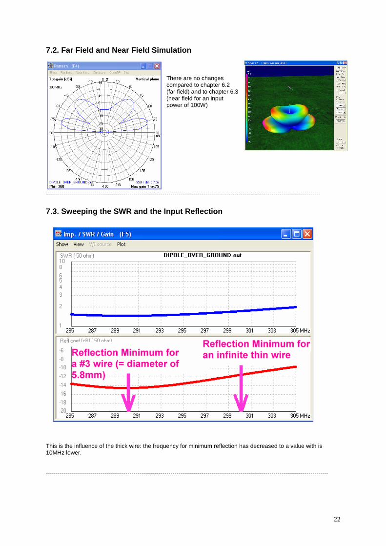
7.2. Far Field and Near Field Simulation
There are no changes compared to chapter 6.2 (far field) and to chapter 6.3 (near field for an input power of 100W)
--------------------------------------------------------------------------------------------------------------------------------------------- 7.3. Sweeping the SWR and the Input Reflection
This is the influence of the thick wire: the frequency for minimum reflection has decreased to a value with is 10MHz lower. -------------------------------------------------------------------------------------------------------------------------------------------------

23
7.4. Sweeping the Antenna Gain At first repeat the simulation of the vertical radiation pattern (see chapter 7.2.), but with an angle resolution of 1 degree.
In this diagram the elevation angle for maximum gain is indicated as Theta = 76 degrees . In the left lower corner of the diagram an azimuth angle of 360 degrees is indicated (this means that we see a “cut” through the 3D pattern at this angle).
Press F7 to enter the following options:
a) Frequency sweep
b) “Gain“
c) Angle resolution of 1 degree
d) Sweep from 280 to 310MHz with a step width of 0. 2MHz
e) Set Theta to 76 degrees and Phi to 0 degrees Now press “Generate “. (Click off the information that in this case no “F/B” data = front to back data are available. Ignore ist and continue with “Generate”)
After the simulation process we see window F5 with the SWR and the input reflection S11.
24
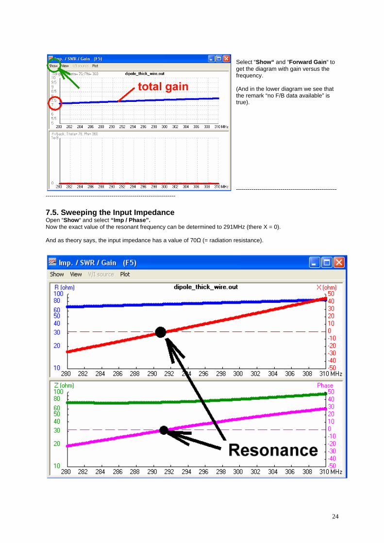
Select “Show“ and “Forward Gain “ to get the diagram with gain versus the frequency. (And in the lower diagram we see that the remark “no F/B data available” is true). ----------------------------------------------------
------------------------------------------------------------------- 7.5. Sweeping the Input Impedance Open “Show “ and select “Imp / Phase”. Now the exact value of the resonant frequency can be determined to 291MHz (there X = 0). And as theory says, the input impedance has a value of 70Ω (= radiation resistance).

25
8. A wonderful toy: the Smith Chart Machine When a simulation is successfully done a Smith chart symbol is highlighted in the menu bar. So we repeat the frequency sweep of the SWR and the Input reflection over a frequency range from 270 to 310MHz with a step width of 0.2MHz and press the Smith chart button. This gives the following screen:
The simulated S11 is shown as black coloured curve . In the right lower corner of the screen you find the actual frequency (here. 270MHz). Use the “right” resp. “left arrow key” on the keyboard to walk through the simulated frequency range and you will here see the S11 value for this frequency. Caution: The information “Mouse” in the next line shows alwa ys the impedance value at the actual mouse cursor position (….and NOT the converted S11 value of the c urve for the simulation frequency). This impedance is indicated in serial and in parallel form. Additionally we find a pink curve and a green vector running through the actual point of the S11 curve. The circle radius gives the S11 magnitude (here: 0.409) and this circle is the way on which we march when a transmission line is connected to the input of the antenna. The phase of S11 is indicated by the green vector (..use the scaling on the circumference of the Smith chart).
26
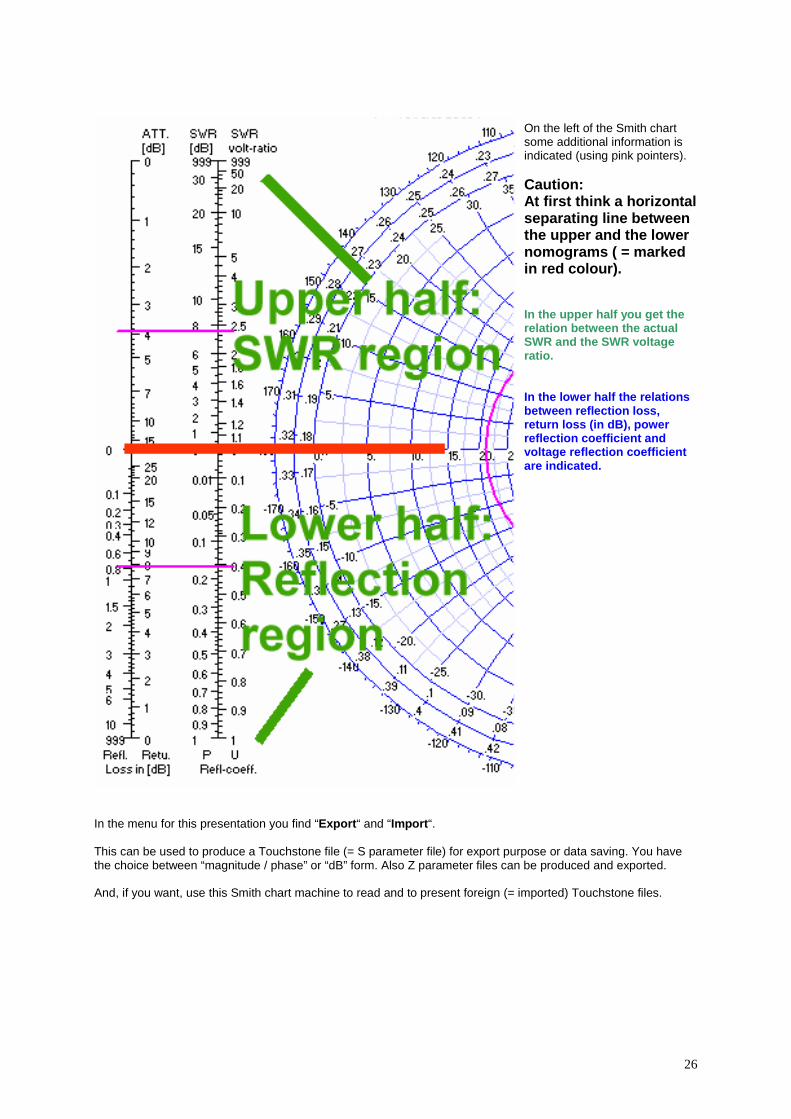
On the left of the Smith chart some additional information is indicated (using pink pointers). Caution: At first think a horizontal separating line between the upper and the lower nomograms ( = marked in red colour). In the upper half you get the relation between the actual SWR and the SWR voltage ratio. In the lower half the relations between reflection loss, return loss (in dB), power reflection coefficient and voltage reflection coefficient are indicated.
In the menu for this presentation you find “Export “ and “Import “. This can be used to produce a Touchstone file (= S parameter file) for export purpose or data saving. You have the choice between “magnitude / phase” or “dB” form. Also Z parameter files can be produced and exported. And, if you want, use this Smith chart machine to read and to present foreign (= imported) Touchstone files.
27
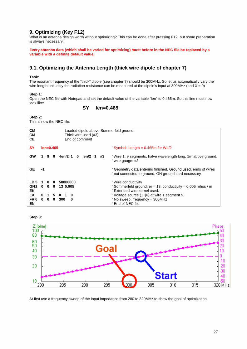
9. Optimizing (Key F12) What is an antenna design worth without optimizing? This can be done after pressing F12, but some preparation is always necessary: Every antenna data (which shall be varied for optimi zing) must before in the NEC file be replaced by a variable with a definite default value. 9.1. Optimizing the Antenna Length (thick wire dipo le of chapter 7) Task: The resonant frequency of the “thick” dipole (see chapter 7) should be 300MHz. So let us automatically vary the wire length until only the radiation resistance can be measured at the dipole’s input at 300MHz (and X = 0) Step 1: Open the NEC file with Notepad and set the default value of the variable “len” to 0.465m. So this line must now look like: SY len=0.465 Step 2: This is now the NEC file: CM Loaded dipole above Sommerfeld ground CM Thick wire used (#3) CE End of comment SY len=0.465 ' Symbol: Length = 0.465m for WL/2 GW 1 9 0 -len/2 1 0 len/2 1 #3 ' Wire 1, 9 segments, halve wavelength long, 1m above ground, ‘ wire gauge: #3 GE -1 ‘ Geometry data entering finished. Ground used, ends of wires ‘ not connected to ground. GN ground card necessary LD 5 1 0 0 58000000 ' Wire conductivity GN 2 0 0 0 13 0.005 ‘ Sommerfeld ground, er = 13, conductivity = 0.005 mhos / m EK ‘ Extended wire kernel used. EX 0 1 5 0 1 0 ' Voltage source (1+j0) at wire 1 segment 5. FR 0 0 0 0 300 0 ‘ No sweep, frequency = 300MHz EN ‘ End of NEC file Step 3:
At first use a frequency sweep of the input impedance from 280 to 320MHz to show the goal of optimization.

28
Step 4: Press F12 and check whether “Optimize “ and “Default “ are set in the upper left corner of the menu. Then select the variable (by clicking in the list) which shall be varied for optimization. In this example we have only “len” as variable and this variable can be activated by a mouse click on its name. But check whether “len” now can be found under “Selected”. At last we set the goal of optimization. It is possible to optimize more but one antenna property but in this case every property must be combined with a figures of merit in % (blue circle in the figure).
Important: Right click on the “X-in” window with its entered value of 100% to get this additional menu. There select “minimize” as optimization goal.
At last press “Start” and wait.
This is the result after 23 seconds and you can press “OK”

29
In the center of the screen changes something and you have now the choice between “Resume” and “Update NEC-File”. Press “Update NEC-File ” to save the necessary modifications. If you now check the file by opening it with Notepad you will find a new value for the wire length with “len=0.4697”. So start a new simulation (F7) with the same frequency sweep as before.
Here is the result:
A fine done job!
---------------------------------------------------------------------------------------------------------------------------------------- 9.2. Parameter Sweep Often it is of interest how some characteristic antenna data (e. g. input impedance) vary not only with frequency but also with special antenna properties (e.g. height over ground). To get a good overview in this case you can use the parameter sweep for this purpose. Here comes an example. 9.2.1. Input Impedance for different Antenna Height s Task: Simulate the input impedance of the thick dipole at f = 300MHz when varying the height over ground between 0.5m and 1,5m in 20 steps. Step 1: Use Notepad to open the NEC file for the following modifications:
a) In the “SY” card add an entry for height as a variable with a default value of 1m (hght=1).
b) Replace the value of 1m in the GW card by the va riable “hght”. CM Example 2 : Loaded dipole above Sommerfeld ground CM Thick wire used (#3) CE End of comment SY len=0.4697, hght=1 ‘ Symbols: Length = 0.4697m for WL/2, height = 1m GW 1 9 0 -len/2 hght 0 len/2 hght #3 ' Wire 1, 9 segments, halve wavelength long, 1m ‘ above ground, wire gauge: #3 GE -1 ‘ Geometry data entering finished. Ground used, ends of wires ‘ not connected to ground. GN ground card necessary LD 5 1 0 0 58000000 ' Wire conductivity on “Load” card GN 2 0 0 0 13 0.005 ‘ Sommerfeld ground, er = 13, conductivity = 0.005 Siemens / m EK ‘ Extended wire kernel used. EX 0 1 5 0 1 0 ' Voltage source (1+j0) at wire 1 segment 5. FR 0 0 0 0 300 0 ‘ No sweep, frequency = 300MHz EN ‘ End of NEC file
30
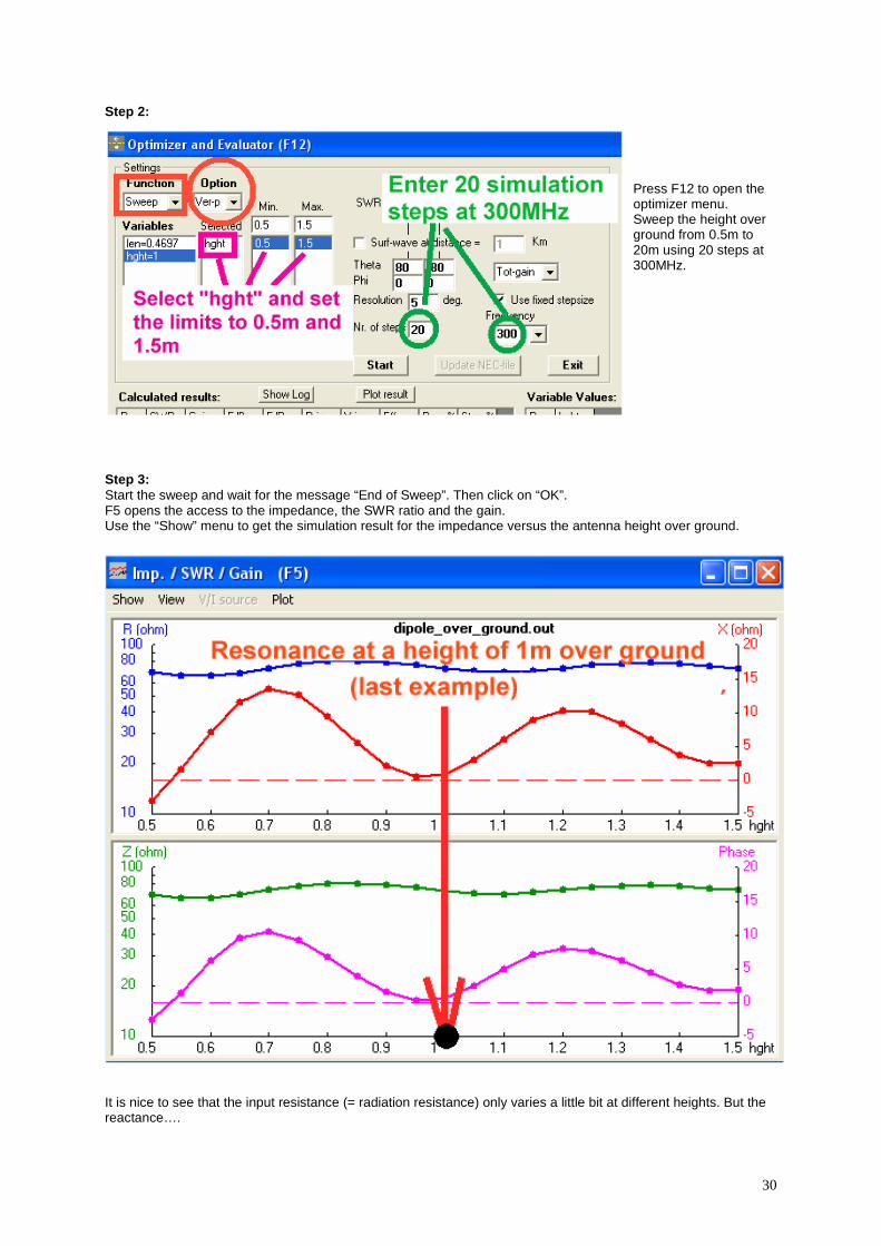
Step 2: Press F12 to open the optimizer menu. Sweep the height over ground from 0.5m to 20m using 20 steps at 300MHz.
Step 3: Start the sweep and wait for the message “End of Sweep”. Then click on “OK”. F5 opens the access to the impedance, the SWR ratio and the gain. Use the “Show” menu to get the simulation result for the impedance versus the antenna height over ground.
It is nice to see that the input resistance (= radiation resistance) only varies a little bit at different heights. But the reactance….

31
9.2.2. Far Field Pattern for different Antenna Heig hts This is not very difficult. First open the windows F3 and F4. F3 is a resume of all simulated patterns. But in F4 only one pattern can be indicated for the choosen height over ground. Click on F4 to activate it and use the horizontal Cursor tabs to regard the pattern collection. (Caution: these are the tabs on the right hand side of your keyboard). The actual height is indicated in the left upper corner of F4, the actual pattern is up lighted in red colour in F3.
32
10. Third Project: Geometry Builder or Text Editor to design a Helix Antenna? 10.1. Fundamentals of Helix-Antenna Design
(Literature: „ARRL Antenna Book“, chapter 19-5. An excellent book which must be recommended…) A helix antenna consists of more but three turns of alumina or copper wire and constant pitch. This gives a circular polarized radiation in direction of the antenna axis (in the left illustration: upwards) and an antenna gain of more but 8dBi. The radiation resistance has a value of approx. 140Ω, if a circumference value of one wavelength is used. Increasing or decreasing the ratio of circumference and wavelength alters the radiation resistance in the same manner. So the perfect matching of the antenna to 50Ω is sometimes heavy work. But one important advantage is the large usable frequency range with nearly constant gain and radiation resistance and the circular polarization. . This antenna shall work over “perfect ground” and so in practice you often find a
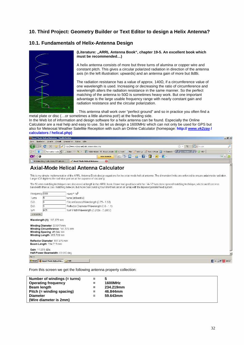
metal plate or disc (…or sometimes a little alumina pot!) at the feeding side. In the Web lot of information and design software for a helix antenna can be found. Especially the Online Calculator are a real help and easy to use. So let us design a 1600MHz which can not only be used for GPS but also for Meteosat Weather Satellite Reception with such an Online Calculator (homepage: http:// www.vk2zay / calculators / helical.php)
From this screen we get the following antenna property collection: Number of windings (= turns) = 5 Operating frequency = 1600MHz Beam length = 234.219mm Pitch (= winding spacing) = 46.844mm Diameter = 59.643mm (Wire diameter is 2mm)

33
10.2. Design using the Geometry Builder Start “main “, then “run “. Select “Geomtry Builder “. Go to the “Helix” card for the necessary entries:
Caution: Let us use 24 segments per turn. For a wire diameter of 2mm the radius is 1mm. Be aware that 3 different units (Meters, Centimetres and Millimetres) are used when entering data! Because “Left / Right handed” is not marked you will automatically get a left hand circular polarization of the radiation. If everything is OK, press “Create” to create the NEC file, which will open automatically. But with (5 turns) x (24 segments per turn) = 120 segments it is a little huge… Save it at once using an adequate namen (e. g. “helix_01.nec“) and close the file and the Geometry Builder.
Go to “Main”, open this NEC file and select “NEC Editor (new)“ in the “Settings” menu. Then press F6. On the “Geometry Card” you find the entry for 120 segments with the all the coordinates and the wire radius of 0.001m On the “Source / Load “ card a voltage source must be applied to “Tag 1“ and “Segment 1“ with a real amplitude of 1V:
The frequency is set to 1600MH. No sweep is used. We use perfect ground and connect wires for Z=0 to ground.
34
On the “Others “ card the Fat wire support must be activated. The last card of the menu is used for comments. Now it is time to save the finished NEC file.
10.3. Far Field Simulation
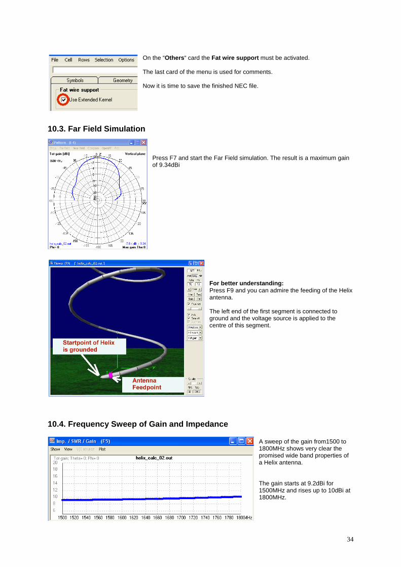
Press F7 and start the Far Field simulation. The result is a maximum gain of 9.34dBi
For better understanding: Press F9 and you can admire the feeding of the Helix antenna. The left end of the first segment is connected to ground and the voltage source is applied to the centre of this segment.
10.4. Frequency Sweep of Gain and Impedance
A sweep of the gain from1500 to 1800MHz shows very clear the promised wide band properties of a Helix antenna. The gain starts at 9.2dBi for 1500MHz and rises up to 10dBi at 1800MHz.
35
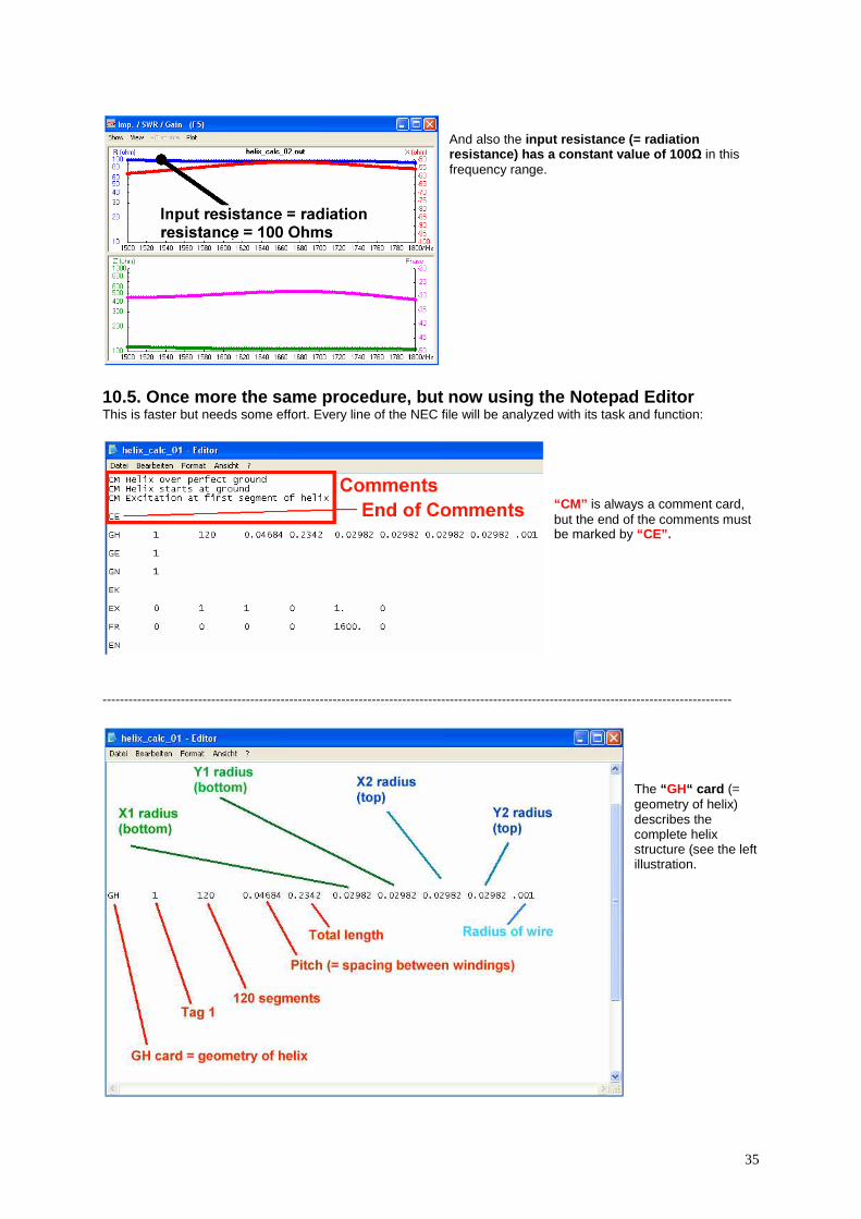
And also the input resistance (= radiation resistance) has a constant value of 100 Ω in this frequency range.
10.5. Once more the same procedure, but now using t he Notepad Editor This is faster but needs some effort. Every line of the NEC file will be analyzed with its task and function:
“CM” is always a comment card, but the end of the comments must be marked by “CE”.
-------------------------------------------------------------------------------------------------------------------------------------------------
The “ GH“ card (= geometry of helix) describes the complete helix structure (see the left illustration.
36
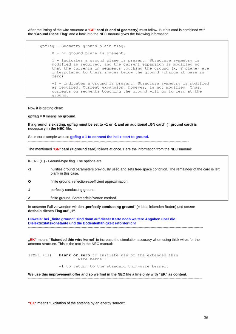
After the listing of the wire structure a “GE” card (= end of geometry ) must follow. But his card is combined with the “Ground Plane Flag “ and a look into the NEC manual gives the following information:
gpflag - Geometry ground plain flag.
0 - no ground plane is present.
1 - Indicates a ground plane is present. Structure symmetry is modified as required, and the current expansion is modified so that the currents in segments touching the ground (x, Y plane) are interpolated to their images below the ground (charge at base is zero)
-1 - indicates a ground is present. Structure symmetry is modified as required. Current expansion, however, is not modified, Thus, currents on segments touching the ground will go to zero at the ground. Now it is getting clear: gpflag = 0 means no ground . If a ground is existing, gpflag must be set to +1 o r -1 and an additional „GN card“ (= ground card) is necessary in the NEC file. So in our example we use gpflag = 1 to connect the helix start to ground. --------------------------------------------------------------------------------------------------------------------------------------- The mentioned “GN“ card (= ground card) follows at once. Here the information from the NEC manual:
IPERF (I1) - Ground-type flag. The options are: -1 nullifies ground parameters previously used and sets free-space condition. The remainder of the card is left blank in this case. O finite ground, reflection-coefficient approximation. 1 perfectly conducting ground. 2 finite ground, Sommerfeld/Norton method. In unserem Fall verwenden wir den „perfectly conducting ground “ (= ideal leitenden Boden) und setzen deshalb dieses Flag auf „1“ . Hinweis: bei „finite ground“ sind dann auf dieser K arte noch weitere Angaben über die Dielektrizitätskonstante und die Bodenleitfähigkeit erforderlich! --------------------------------------------------------------------------------------------------------------------------------------------------- „ EK“ means “Extended thin wire kernel “ to increase the simulation accuracy when using thick wires for the antenna structure. This is the text in the NEC manual:
ITMP1 (I1) - Blank or zero to initiate use of the extended thin- wire kernel.
-1 to return to the standard thin-wire kernel. We use this improvement offer and so we find in the NEC file a line only with “EK” as content. -------------------------------------------------------------------------------------------------------------------------------------------------- “EX “ means “Excitation of the antenna by an energy source“:

37
„0“ = a voltage source is applied „1“ = Tag 1 is used for excitation „1“ = number of the segment of this tag, where the voltage source is applied to (..at the centre of this segment) „0“ = empty field on this card „1 0“ = real and imaginary part of the applied complex voltage (here: 1 + j0). That means that a real voltage of 1V
is applied ------------------------------------------------------------------------------------------------------------------------------------- „ FR“ = frequency sweep information . „0“ = linear sweep (1 = logarithmic sweep) „0“ = no frequency steps used. So only the frequenca start value is used for a simulation. „0 0“ = two empty fields on this card „1600“ = start value of frequency sweep = 1600MHz „0“ = frequency step width = 0 MHz for our example -------------------------------------------------------------------------------------------------------------------------------------- „EN“ = end of NEC file ------------------------------------------------------------------------------------------------------------------------------------- 10.6. Once more: Far Field Simulation
This the form of the diagram is nearly identical to the patter in chapter 9.3. One difference is the reduced maximum gain calculation (8,9dBi compared to 9,3dBi in chapter 9.3.)
Pressing F9 shows that the helix start is connected to ground and the voltage source applied to the centre of the first segment.

38
10.7. Once more: Frequency Sweep of Gain and Impeda nce The gain curve is identical to chapter 9.4. but the absolute values are reduced by 0.4dB. The impedance curves are absolutely identical to chapter 9.4. and the radiation resistance has its correct value of 100Ω.
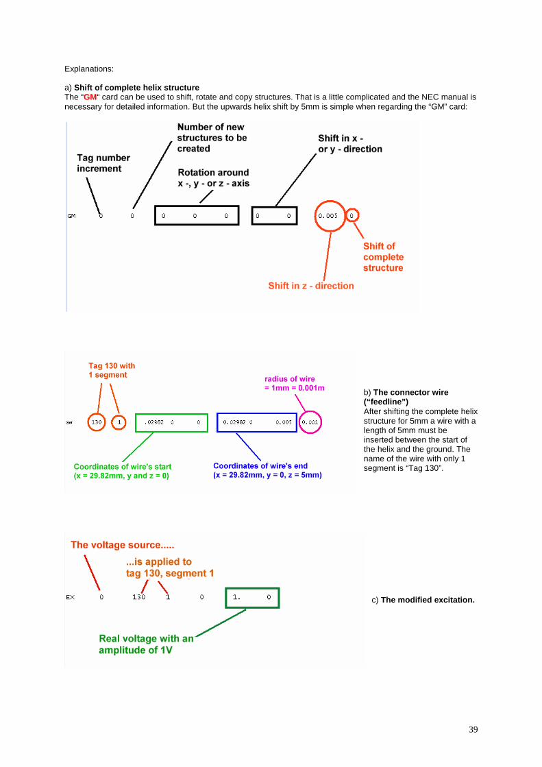
------------------------------------------------------------------------------------- 10.8. Feeding the Antenna by a short Piece of Wire This is the reality because normally an SMA or N connector is used to feed the helix. This connector is screwed on the other side of the ground plane alumina plate and feeds the antenna through a drilled hole in the plate. So the helix structure is “lifted” to avoid a contact between the first antenna winding and the alumina plate. In the NEC file
a) The antenna structure must be lifted by 5 mm b) A new wire must be added from the helix start to the perfect ground. The voltage source for excitation is
then connected to the centre of this wire. This can be done in the NEC file using Notepad:
This is the new file with modified comments, a “lif ted” helix (“GM” = geometry move), an added piece o f wire and a modified excitation point at the centre of the piece of wire.
39
Explanations: a) Shift of complete helix structure The “GM“ card can be used to shift, rotate and copy structures. That is a little complicated and the NEC manual is necessary for detailed information. But the upwards helix shift by 5mm is simple when regarding the “GM” card:
b) The connector wire (“feedline”) After shifting the complete helix structure for 5mm a wire with a length of 5mm must be inserted between the start of the helix and the ground. The name of the wire with only 1 segment is “Tag 130”.
c) The modified excitation.

40
F7 starts the far field simulation . No changes… When pressing F9 you can see the added new feedline and the shifted helix structure (voltage source applied to the centre of this wire = marked in pink).
And now the sweep results from 1500 to1800MHz.
The gain: no changes…
But the impedance has changed: Lifting the helix structure increases the “height of the antenna over ground” and this gives a new radiation resistance of 150 Ω. Also the reactance differs now…

41
Appendix: Short overview of the most important „Cards“ -------------------------------------------------------------------------------------------------------------------------------- “CM“ = comment with a maximum of 30 characters in one line -------------------------------------------------------------------------------------------------------------------------------- ” CE“ = end of comments ------------------------------------------------------------------------------------------------------------------------------- “ SY“ = “Symbol “ = definition of a Variable (or more, separated by a comma, for optimizing or
parametric sweep). ------------------------------------------------------------------------------------------------------------------------------- “ GW“ = “Geometry of wire“. Entries are necessary in the following range: :
Tag number / number of segments / XYZ coordinates of start point / XYZ coordinates of end point / wire radius in Meters.
------------------------------------------------------------------------------------------------------------------------------- “ GM“ = “Geometry Move “. Structures can be rotated, shifted and copied (For details see the NEC2 manual).
But shifting a structure is simple. The necessary line for a 5 mm (upwards) shift is GM 0 0 0 0 0 0 0 0.005 0 -------------------------------------------------------------------------------------------------------------------------------- “ GE“ = “End of geometry” . The following number says:
“0“ = no ground (= free space)
“-1“ or “1“ says: ground is present. But now an add itional ground card is obligatory. The NEC2 manual says:
0 - no ground plane is present. 1 - Indicates a ground plane is present. Structure symmetry is modified as required, and the current expansion is modified so that the currents on segments touching the ground (x, Y plane) are interpolated to their images below the ground (charge at base is zero) -1 - indicates a ground is present. Structure symmetry is modified as required. Current expansion, however, is not modified, Thus, currents on segments touching the ground will go to zero at the ground.
-------------------------------------------------------------------------------------------------------------------------------- “ LD“ = “Loading of a segment “. See the NEC manual or the online help to use this option
with success.
Very often only “LD 5“ is used and this gives the conductance of the antenna wire. The line starts with the tag number and after two empty fields follows the conductance
(e. g. “5.8001E7“ for copper in mhos / m). ---------------------------------------------------------------------------------------------------------- “ GN“ = Ground card . This card is always obligatory if GE is followed by a number. Please have a look at the NEC2 manual for correct usage of “freespace” or “finite
ground” or “perfect ground” or “Sommerfeld – Norton ground”. ---------------------------------------------------------------------------------------------------------- “ EK“ = „Extended thin wire kernel “. This increases the accuracy when using non infinite thin
wires. The manual says:
ITMP1 (I1) - Blank or zero to initiate use of the extended thin- wire kernel.
-1 to return to the standard thin-wire kernel. -------------------------------------------------------------------------------------------------------------------------

42
“ EX“ = „Exitation “ of the structure by an energy source. Example: EX 0 1 5 0 1 0 “0“ = a voltage source is used The source is applied to tag 1 / segment 5 „0“ = stands for an empty field
“1 0“ is a real voltage source (no imaginary part) with an amplitude of 1V ------------------------------------------------------------------------------------------------------------------ “ FR“ = “Frequency sweep”.
(Explained by an example line: “FR 0 1 0 0 300 0”)
“0“ = „linear sweep “ (“1” = logarithmic sweep) “1“ = only 1 frequency step. „0 0“ = two empty fields. „300“ = sweep starts at a frequency of 300MHz „0“ = frequency step width is 0 MHz. This programs a simulation at only one frequency
(here. 300MHz) --------------------------------------------------------------------------------------------------------- “ EN“ = “End of Run“ ---------------------------------------------------------------------------------------------------------