![Design of a Simulation Tool for Steam Assisted Gravity ... · SAGD [5, 6]. The future development of a software tool for SAGD process simulation for production and tooling design](https://static.fdocuments.in/doc/165x107/5fe7e08271960123b454f877/design-of-a-simulation-tool-for-steam-assisted-gravity-sagd-5-6-the-future.jpg)
SIMULATION DESIGN TOOL - · PDF fileSimulation Design Tool INDEX Sr. No. Title Page Date Sign...
45
SHANKERSINH VAGHELA BAPU INSTITUTE OF TECHNOLOGY SIMULATION DESIGN TOOL LABORATORY MANUAL B.E. 4 th SEMESTER-2015-16 SHANKERSINH VAGHELA BAPU INSTITUTE OF TECHNOLOGY Gandhinagar-Mansa Road, PO. Vasan, Gandhinagar District, Gujarat, Pin. 382650
Transcript of SIMULATION DESIGN TOOL - · PDF fileSimulation Design Tool INDEX Sr. No. Title Page Date Sign...

SHANKERSINH VAGHELA BAPU INSTITUTE OF TECHNOLOGY
SIMULATION DESIGN TOOL
LABORATORY MANUAL
B.E. 4th SEMESTER-2015-16
SHANKERSINH VAGHELA BAPU INSTITUTE OF TECHNOLOGY
Gandhinagar-Mansa Road, PO. Vasan,
Gandhinagar District, Gujarat,
Pin. 382650

Shankersinh Vaghela Bapu Institute Of Technology.
Simulation Design Tool
1
Simulation Design Tool
INDEX
Sr.
No.
Title Page Date Sign Grade
1.a
1.b
Simulate and study of half-wave, using
Multisim.
Simulate and study of full-wave, using
Multisim.
2. Simulate and study of bridge-rectifier
using Multisim.
3.a
3.b
Stimulate and Study Positive Clipper
circuits using Multisim.
Stimulate and Study Negative Clipper
circuits using Multisim.
4.a
4.b
Stimulate and Study Positive Clamper
circuits using Multisim
Stimulate and Study Negative Clamper
circuits using Multisim
5. Stimulate and Study Voltage Regulator
using Multisim.
6. Stimulate and Study logical expression
using Multisim
7.a
7.b
Simulate Full adder using Multisim and
determine its truth table.
Simulate Full adder using Multisim and
determine its truth table.

Shankersinh Vaghela Bapu Institute Of Technology.
Simulation Design Tool
2
8. Simulate a 3-bit synchronous counter
and determine its counter sequence
using Multisim.
9. Simulate a 4-bit Asynchronous counter
and determine its counter sequence
using Multisim.
10. Introduction to PCB Design

Shankersinh Vaghela Bapu Institute Of Technology.
Simulation Design Tool
3
EXPERIMENT:- 1
[A] AIM: Stimulate and Study half-wave Rectifier using Multisim.
EQUIPMENTS: [1].Transformer NLT_PQ_4_12.
[2].Oscilloscope XSC1.
[3].Resistor 2k.
[4].Diode Virtual.
[5].Voltage Source.
THEORY: The process of converting an alternating voltage/current to a
unidirectional voltage/current is called rectification. A diode offers very
low resistance when forward biased and very high resistance when
reverse biased. Hence, it can be used as rectifier. The rectified output is a
pulsating unidirectional voltage/current. A filter is necessary after rectifier
to convert pulsating waveform to dc.
Half wave rectifier: During positive half cycle, the diode is forward biased. Hence,
current flows through load resistor. During negative half cycle, the diode
is reverse biased and is equivalent to open circuit. Therefore current
through load is zero. Thus, the diode conducts only for one half cycles
and results in half wave rectified output. Half wave rectifier is simple and
low cost circuit but it has very high ripple, lower efficiency.

Shankersinh Vaghela Bapu Institute Of Technology.
Simulation Design Tool
4
CIRCUIT DIAGRAM:
Figure 1
PROCEDURE:
[1]Complete the circuit as per the fig. (1) for half wave rectifier.
[2]Connect the CRO across the load.
[3]Switch on the supply.
[4]Keep the CRO in ground mode and Switch the CRO to DC mode
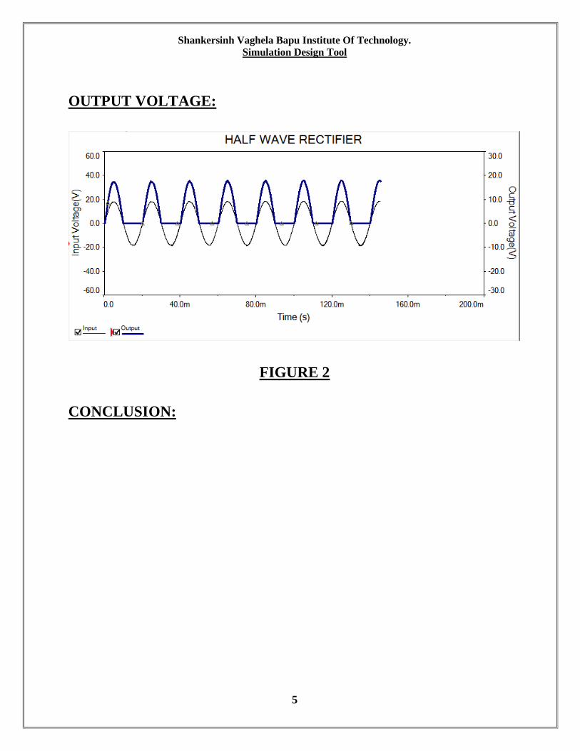
[5]Observe the half wave rectifier output voltage
Shankersinh Vaghela Bapu Institute Of Technology.
Simulation Design Tool
5
OUTPUT VOLTAGE:
FIGURE 2
CONCLUSION:

Shankersinh Vaghela Bapu Institute Of Technology.
Simulation Design Tool
6
EXPERIMENT:-1
[B] AIM:
Stimulate and Study Full-wave Rectifier using Multisim.
EQUIPMENTS:
[1].Transformer NLT_PQ_4_12.
[2].Oscilloscope XSC1.
[3].Resistor 2k.
[4].Diode Virtual. (2)
[5].Voltage Source.
THEORY:
The process of converting an alternating voltage/current to a
unidirectional voltage/current is called rectification. A diode offers very
low resistance when forward biased and very high resistance when
reverse biased. Hence, it can be used as rectifier. The rectified output is a
pulsating unidirectional voltage/current. A filter is necessary after rectifier
to convert pulsating waveform to dc.
Full wave rectifier: The full wave rectifier consists of a center-tap transformer, which
results in equal voltages above and below the center-tap. During the
positive half cycle, positive voltage appears at the anode of D1 while
negative voltage at the anode of D2. So diode D1 is forward biased and it
results in current through load. During negative half cycle, the positive
voltage appears at the anode of D2 and hence it is forward biased
resulting in current through load. At the same instant a negative voltage
appears at the anode of D1, thus reverse biasing it and hence D1 does not
conduct. The current through the load during both half cycles is in the

Shankersinh Vaghela Bapu Institute Of Technology.
Simulation Design Tool
7
same direction hence it is sum of individual currents. The individual
currents and voltages are combined in the load and therefore their average
values are double that obtained in a half wave rectifier. In full wave
rectifier, ripple is reduced, efficiency is improved. And as equal current
flows through secondary during both the half cycle, core does not
saturate. The demerits of full wave rectifier are : output voltage is half the
secondary voltage and diodes with high PIV ratings are required.
CIRCUIT DIAGRAM:
Figure-1
PROCEDURE:
[1]Complete the circuit as per the fig. (1) for Full wave rectifier.
[2]Connect the CRO across the load.
Shankersinh Vaghela Bapu Institute Of Technology.
Simulation Design Tool
8
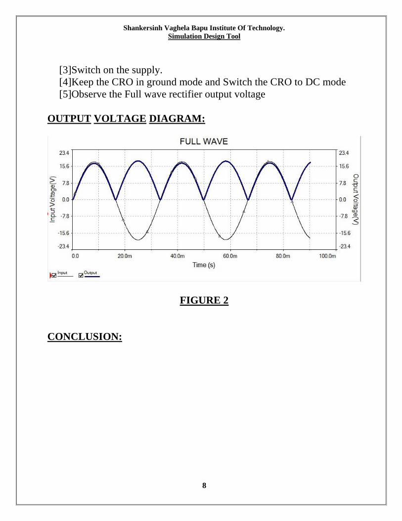
[3]Switch on the supply.
[4]Keep the CRO in ground mode and Switch the CRO to DC mode
[5]Observe the Full wave rectifier output voltage
OUTPUT VOLTAGE DIAGRAM:
FIGURE 2
CONCLUSION:

Shankersinh Vaghela Bapu Institute Of Technology.
Simulation Design Tool
9
EXPERIMENT: - 2
AIM:
Stimulate and Study Bridge-wave Rectifier using Multisim.
EQUIPMENTS:
[1].Transformer NLT_PQ_4_12.
[2].Oscilloscope XSC1.
[3].Resistor 2k.
[4].Diode Virtual. (4)
[5].Voltage Source.
THEORY:
The process of converting an alternating voltage/current to a
unidirectional voltage/current is called rectification. A diode offers very
low resistance when forward biased and very high resistance when
reverse biased. Hence, it can be used as rectifier. The rectified output is a
pulsating unidirectional voltage/current. A filter is necessary after rectifier
to convert pulsating waveform to dc.
Bridge rectifier: This circuit does not required center-tap transformer. During the
positive half cycle, diodes D1 and D2 are forward biased and D3 and D4
are reverse biased. Thus, current flows in the circuit due to D1 and D2.
During the positive half cycle, diodes D1 and D2 are forward biased and
D3 and D4 are reverse biased. Thus, current flows in the circuit due to D1
and D2. During the negative half cycle, diodes D3 and D4 are forward
biased and D1 and D2 are reverse biased which results in a current in the
same direction. Thus the current flows for the whole cycle across the load
in one direction resulting in full wave rectification. Since bridge rectifier
does not required center-tapped transformer, its cost, weight and size are
lesser compared to a full wave rectifier. Diode with lesser PIV can be
used in bridge rectifier compared to full wave rectifier.

Shankersinh Vaghela Bapu Institute Of Technology.
Simulation Design Tool
10
CIRCUTI DIAGRAM:
FIGURE 1
PROCEDURE:
[1]Complete the circuit as per the fig. (1) for Bridge rectifier.
[2]Connect the CRO across the load.
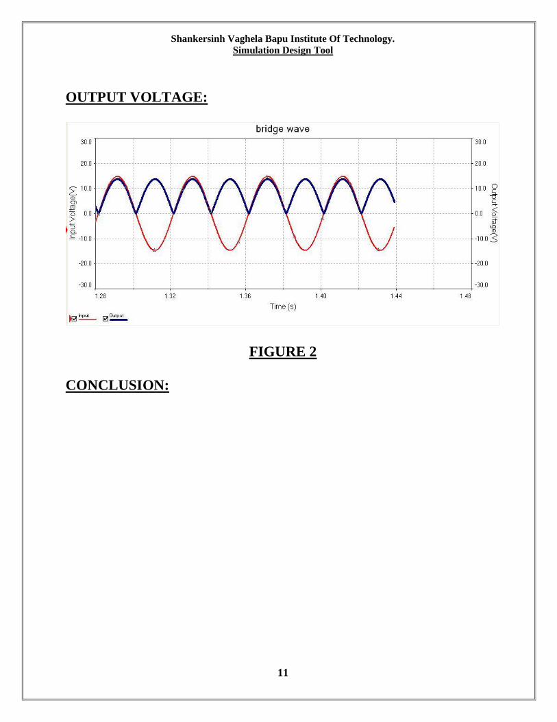
[3]Switch on the supply.
[4]Keep the CRO in ground mode and Switch the CRO to DC mode
[5]Observe the Bridge rectifier output voltage.
Shankersinh Vaghela Bapu Institute Of Technology.
Simulation Design Tool
11
OUTPUT VOLTAGE:
FIGURE 2
CONCLUSION:

Shankersinh Vaghela Bapu Institute Of Technology.
Simulation Design Tool
12
EXPERIMENT:-3 [A]
AIM:
Stimulate and Study Positive Clipper circuits using Multisim.
EQUIPMENTS:
[1]XFG1
[2]Resistor 2K.
[3]Oscilloscope XSC1
[4]Virtual Diode.
THEORY: The circuit used to limit or clip the extremities of the ac signal
is called the limiter or clipper. Limiters can transform a sine wave into a
rectangular wave. It can limit either the positive or negative amplitude of
an ac voltage. It can also perform other useful wave shaping functions.
The unidirectional characteristics of semiconductor diodes permit to
serve as limiter. In Figure 1, a sine wave signal of amplitude V in is
applied to the input. During the positive half cycle of the input signal,
diode D is reversed biased and cannot conduct. Hence the output obtained
at the output terminals is zero. During the negative half cycle of the input
signal, diode D is forward biased and current can flow in the circuit.
Hence at the output terminal, the output voltage Vo will be developed
which will be having full negative half cycles and clipped positive half
cycles. This circuit is known as positive clipper because the diode is in
series with the output terminal and the output is clipped on the positive
side.

Shankersinh Vaghela Bapu Institute Of Technology.
Simulation Design Tool
13
CIRCUIT DIAGRAM:
Figure-1
PROCEDURE:
POSITIVE CLIPPER
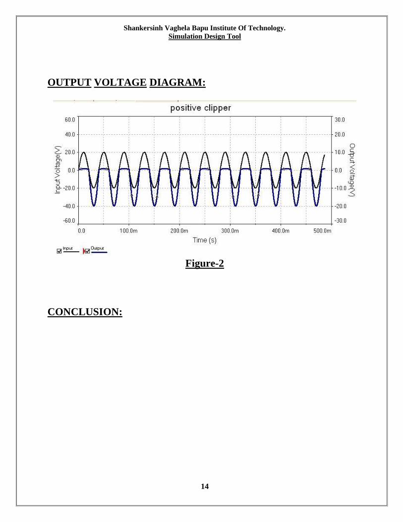
[1]Connect the circuit of Figure-1 and apply a sine wave voltage of 50 Hz
(Vin max.15V) at the input terminal using audio signal generator
XFG1.
[2]Observe the output voltage Vo in waveform in Oscilloscope.
Shankersinh Vaghela Bapu Institute Of Technology.
Simulation Design Tool
14
OUTPUT VOLTAGE DIAGRAM:
Figure-2
CONCLUSION:

Shankersinh Vaghela Bapu Institute Of Technology.
Simulation Design Tool
15
EXPERIMENT:-3
[B]
AIM:
Stimulate and Study Negative Clipper circuits using Multisim.
EQUIPMENTS:
[1]XFG1
[2]Resistor 2K.
[3]Oscilloscope XSC1
[4]Virtual Diode.
THEORY: The circuit used to limit or clip the extremities of the ac signal is
called the limiter or clipper. Limiters can transform a sine wave into a
rectangular wave. It can limit either the positive or negative amplitude of
an ac voltage. It can also perform other useful wave shaping functions.
The unidirectional characteristics of semiconductor diodes permit to
serve as limiter. In Figure 1, a sine wave signal of amplitude Vin is
applied to the input. During the positive half cycle of the input signal,
diode D is reversed biased and cannot conduct. Hence the output obtained
at the output terminals is zero. During the negative half cycle of the input
signal, diode D is forward biased and current can flow in the circuit.
Hence at the output terminal, the output voltage Vo will be developed
which will be having full negative half cycles and clipped positive half
cycles. By reversing the polarity of diode negative clipper can be
realized which can give the output voltage Vo with full positive half
cycles and clipped negative half cycles.

Shankersinh Vaghela Bapu Institute Of Technology.
Simulation Design Tool
16
CIRCUIT DIAGRAM:
Figure-3
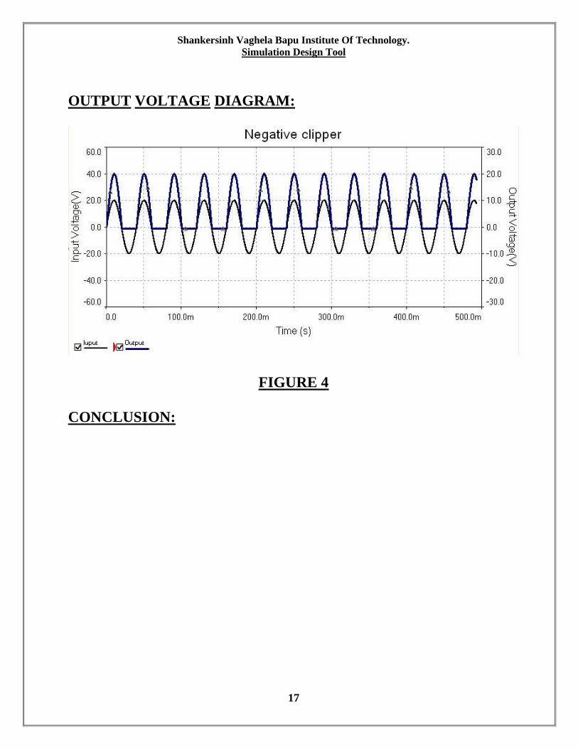
PROCEDURE: [1]Connect the circuit of Figure-3 and apply a sine wave voltage of 50
Hz (Vin max.15V) at the input terminal using audio signal generator
XFG1.
[2]Observe the output voltage Vo in waveform in Oscilloscope.
Shankersinh Vaghela Bapu Institute Of Technology.
Simulation Design Tool
17
OUTPUT VOLTAGE DIAGRAM:
FIGURE 4
CONCLUSION:

Shankersinh Vaghela Bapu Institute Of Technology.
Simulation Design Tool
18
EXPERIMENT:-4 [A]
AIM:
Stimulate and Study Positive Clamper circuits using Multisim.
EQUIPMENTS:
[1]XFG1
[2]Resistor 200K.
[3]Oscilloscope XSC1
[4]Virtual Diode.
[5]Capacitor 100 pf
THEORY:
The circuit that does not change the shape of the input waveform but
only adds a D.C. level to the input waveform is known as clamper, d.c.
Restorer or dc inserter.
In the circuit of Figure 1, during the negative half cycle of the input
sine wave signal of 15 V (peak-to-peak), the diode D will conduct and the
capacitor C will charge to the 5Vpeak value of the negative half cycle
through the low resistance path of the forward biased diode. During the
positive half cycle of the input sine wave signal, the diode D can not
conduct and the capacitor C will try to discharge through R. If the
discharge time constant RC is large as compared to the time period of the
input sine wave, the capacitor will lose very little of its charge and will
hold the charged value of 5 V across it. Now during the next negative half
cycle of the input sine wave signal, the negative input voltage will be
cancelled by the positive voltage across the capacitor and diode cannot
conduct. Hence, effectively 5 V is added by this positive clamper to the
input sine wave. The output wave will have D.C. Level of 5 V and it will
vary from 0 V to 10 V.
Shankersinh Vaghela Bapu Institute Of Technology.
Simulation Design Tool
19
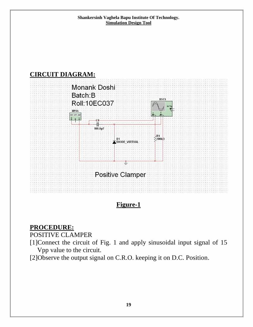
CIRCUIT DIAGRAM:
Figure-1
PROCEDURE:
POSITIVE CLAMPER
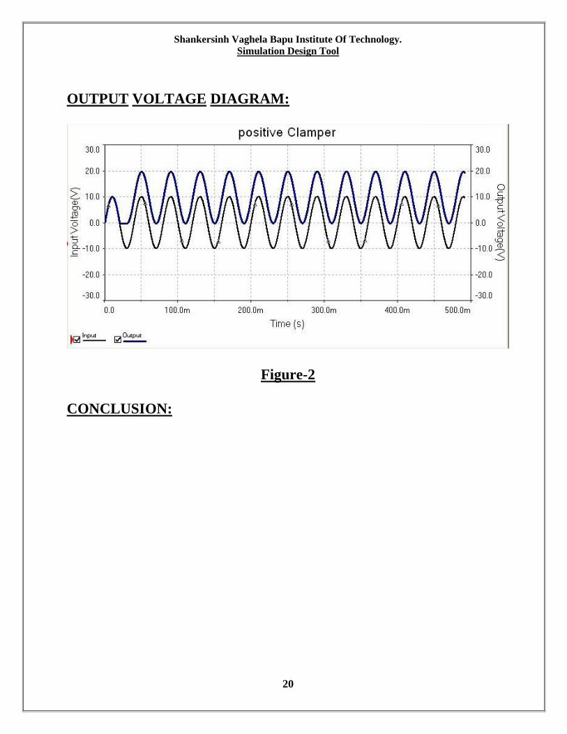
[1]Connect the circuit of Fig. 1 and apply sinusoidal input signal of 15
Vpp value to the circuit.
[2]Observe the output signal on C.R.O. keeping it on D.C. Position.
Shankersinh Vaghela Bapu Institute Of Technology.
Simulation Design Tool
20
OUTPUT VOLTAGE DIAGRAM:
Figure-2
CONCLUSION:

Shankersinh Vaghela Bapu Institute Of Technology.
Simulation Design Tool
21
EXPERIMENT:-4
[B]
AIM:
Stimulate and Study Negative Clamper circuits using Multisim.
EQUIPMENTS:
[1]XFG1
[2]Resistor 200K.
[3]Oscilloscope XSC1
[4]Virtual Diode.
[5]Capacitor 100 pf
THEORY: The circuit that does not change the shape of the input waveform but
only adds a D.C. level to the input waveform is known as clamper, d.c.
Restorer or dc inserter.
In the circuit of Figure 1, during the negative half cycle of the input
sine wave signal of 15 V (peak-to-peak), the diode D will conduct and the
capacitor C will charge to the 5Vpeak value of the negative half cycle
through the low resistance path of the forward biased diode.Negative
clamper works on the similar principle as that of the positive clamper and
can add a negative D.C. Level to the input wave. In the circuit shown in
Figure 3, the polarity of the diode D has been reversed. The capacitor C
will charge during the positive half cycle of the input sine wave signal and
will hold the peak value of the half cycle across it. The circuit effectively
will add - 5 V to the input sine wave and the output will vary from 0 V to
- 10 V with D.C. Value equal to - 5 V.
Shankersinh Vaghela Bapu Institute Of Technology.
Simulation Design Tool
22
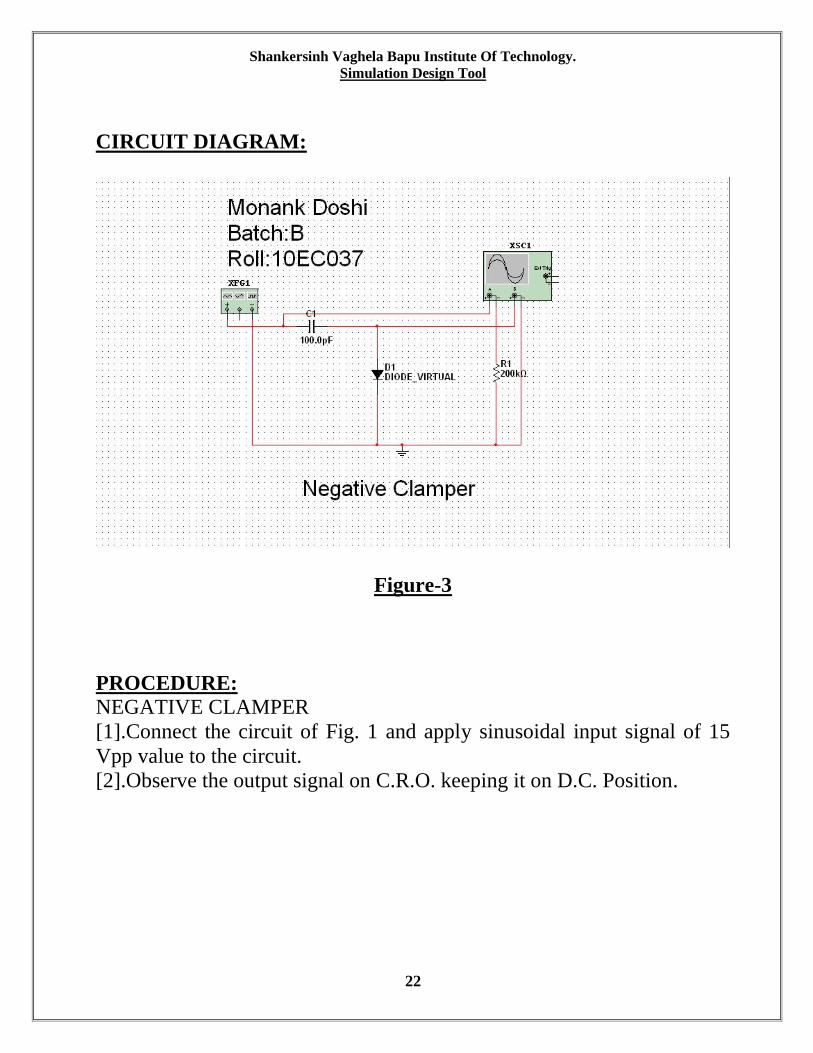
CIRCUIT DIAGRAM:
Figure-3
PROCEDURE:
NEGATIVE CLAMPER
[1].Connect the circuit of Fig. 1 and apply sinusoidal input signal of 15
Vpp value to the circuit.
[2].Observe the output signal on C.R.O. keeping it on D.C. Position.
Shankersinh Vaghela Bapu Institute Of Technology.
Simulation Design Tool
23
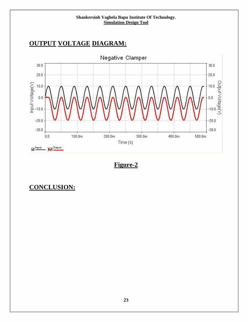
OUTPUT VOLTAGE DIAGRAM:
Figure-2
CONCLUSION:
Shankersinh Vaghela Bapu Institute Of Technology.
Simulation Design Tool
24
EXPERIMENT:- 5
AIM: Stimulate and Study Voltage Regulator using Multisim.
EQUIPMENTS: [1].Function generator.
[2].Oscilloscope XSC1.
[3].Resistor 2k.
[4]. Line voltage.
THEORY:
The Digilab board can use any power supply that creates a DC
voltage between 6 and 12 volts. A 5V voltage regulator (7805) is used to
ensure that no more than 5V is delivered to the Digilab board regardless
of the voltage present at the J12 connector (provided that voltage is less
than 12VDC). The regulator functions by using a diode to clamp the
output voltage at 5VDC regardless of the input voltage - excess voltage is
converted to heat and dissipated through the body of the regulator. If a
DC supply of greater than 12V is used, excessive heat will be generated,
and the board may be damaged. If a DC supply of less than 5V is used,
insufficient voltage will be present at the regulators output.
If a power supply provides a voltage higher than 7 or 8 volts, the
regulator must dissipate significant heat. The "fin" on the regulator body
(the side that protrudes upward beyond the main body of the part) helps to
dissipate excess heat more efficiently. If the board requires higher
currents (due to the use of peripheral devices or larger breadboard
circuits), then the regulator may need to dissipate more heat. In this case,
the regulator can be secured to the circuit board by fastening it with a
screw and nut (see below). By securing the regulator tightly to the circuit
board, excess heat can be passed to the board and then radiated away.
Shankersinh Vaghela Bapu Institute Of Technology.
Simulation Design Tool
25
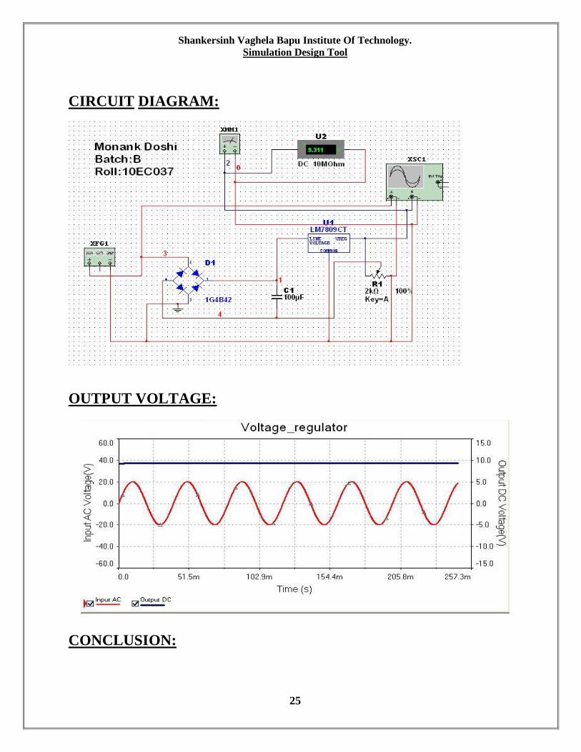
CIRCUIT DIAGRAM:
OUTPUT VOLTAGE:
CONCLUSION:

Shankersinh Vaghela Bapu Institute Of Technology.
Simulation Design Tool
26
EXPERIMENT: - 6
AIM: Stimulate and Study logical expression using Multisim.
EQUIPMENTS:
[1].AND GATE.
[2].OR GATE.
[3].NOT GATE.
THEORY:
LOGIC EXPRESSION:-
Minterms:-
Y= ∑ m(0,1,2,3,5,7,8,10,15)
K-map
Shankersinh Vaghela Bapu Institute Of Technology.
Simulation Design Tool
27
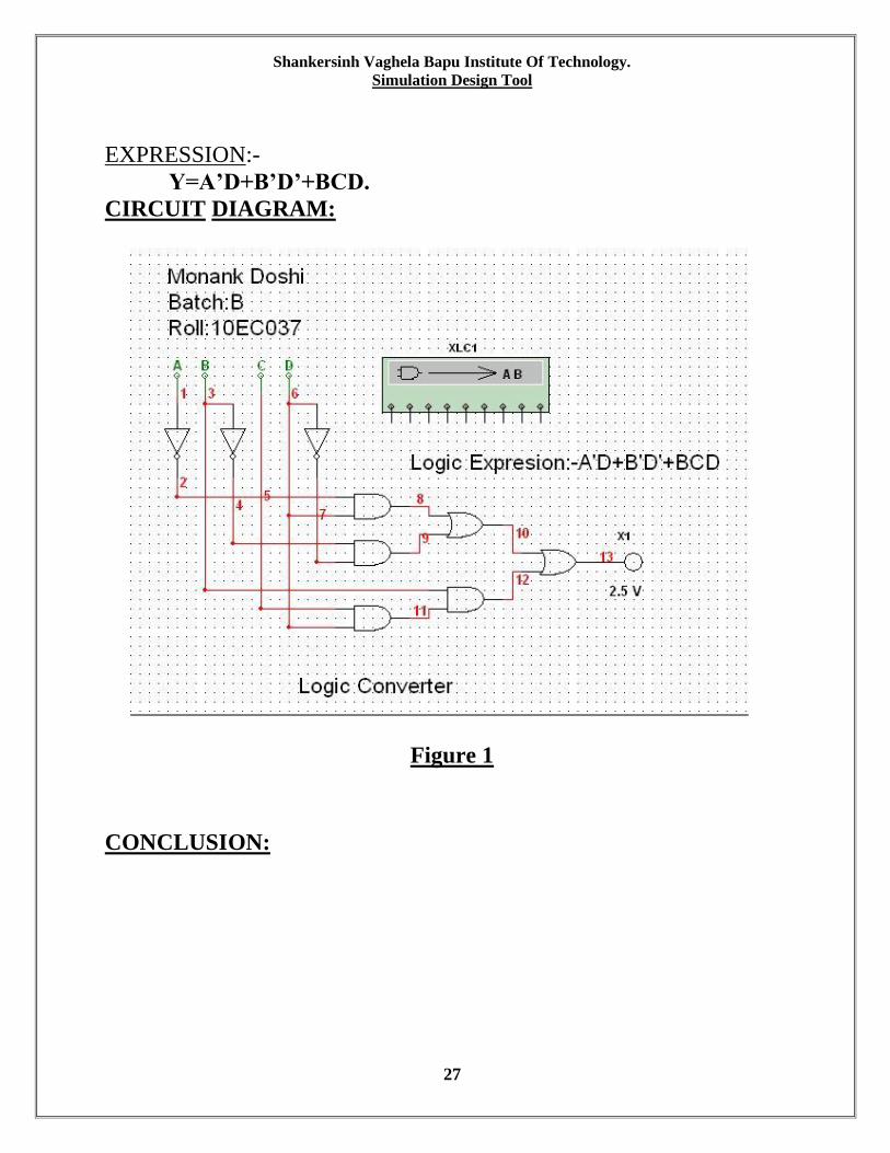
EXPRESSION:-
Y=A’D+B’D’+BCD.
CIRCUIT DIAGRAM:
Figure 1
CONCLUSION:
Shankersinh Vaghela Bapu Institute Of Technology.
Simulation Design Tool
28
EXPERIMENT: - 7
[A]
AIM: Simulate Full adder using Multisim and determine its truth table.
EQUIPMENTS: [1].AND GATE.
[2].OR GATE.
[3].NOT GATE.
[4].PROBE.
[5]. VOLTAGE SOURCE.
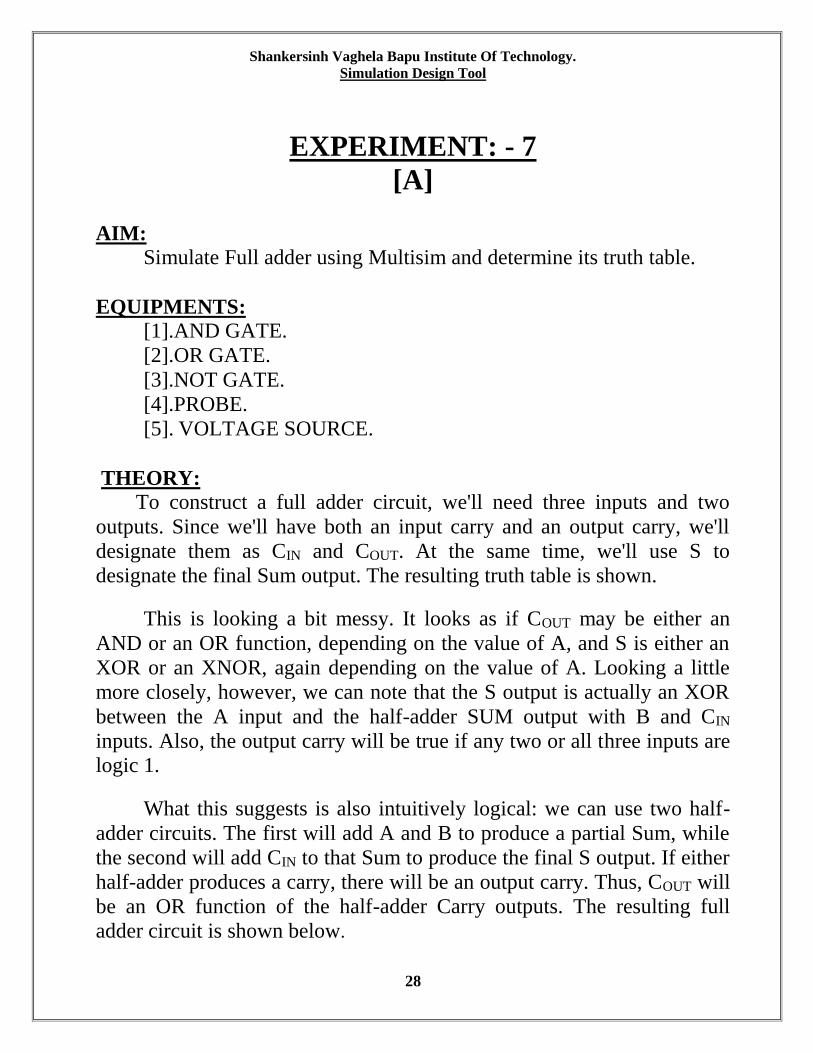
THEORY: To construct a full adder circuit, we'll need three inputs and two
outputs. Since we'll have both an input carry and an output carry, we'll
designate them as CIN and COUT. At the same time, we'll use S to
designate the final Sum output. The resulting truth table is shown.
This is looking a bit messy. It looks as if COUT may be either an
AND or an OR function, depending on the value of A, and S is either an
XOR or an XNOR, again depending on the value of A. Looking a little
more closely, however, we can note that the S output is actually an XOR
between the A input and the half-adder SUM output with B and CIN
inputs. Also, the output carry will be true if any two or all three inputs are
logic 1.
What this suggests is also intuitively logical: we can use two half-
adder circuits. The first will add A and B to produce a partial Sum, while
the second will add CIN to that Sum to produce the final S output. If either
half-adder produces a carry, there will be an output carry. Thus, COUT will
be an OR function of the half-adder Carry outputs. The resulting full
adder circuit is shown below.
Shankersinh Vaghela Bapu Institute Of Technology.
Simulation Design Tool
29
TRUTH TABLE:-
CIRCUIT:-
INPUTS OUTPUTS
A B C COUT S
0 0 0 0 0
0 0 1 0 1
0 1 0 0 1
0 1 1 1 0
1 0 0 0 1
1 0 1 1 0
1 1 0 1 0
1 1 1 1 1
Shankersinh Vaghela Bapu Institute Of Technology.
Simulation Design Tool
30
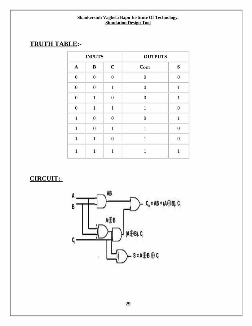
CIRCUIT DIAGRAM:
OUTPUT DIAGRAM:
CONCLUSION:
Shankersinh Vaghela Bapu Institute Of Technology.
Simulation Design Tool
31
EXPERIMENT:- 7
[B]
AIM: Simulate Full Subtractor using multisim and determine its truth
table.
EQUIPMENTS: [1].AND GATE.
[2].OR GATE.
[3].XOR GATE.
[4].PROBE.
[5]. VOLTAGE SOURCE.
THEORY:
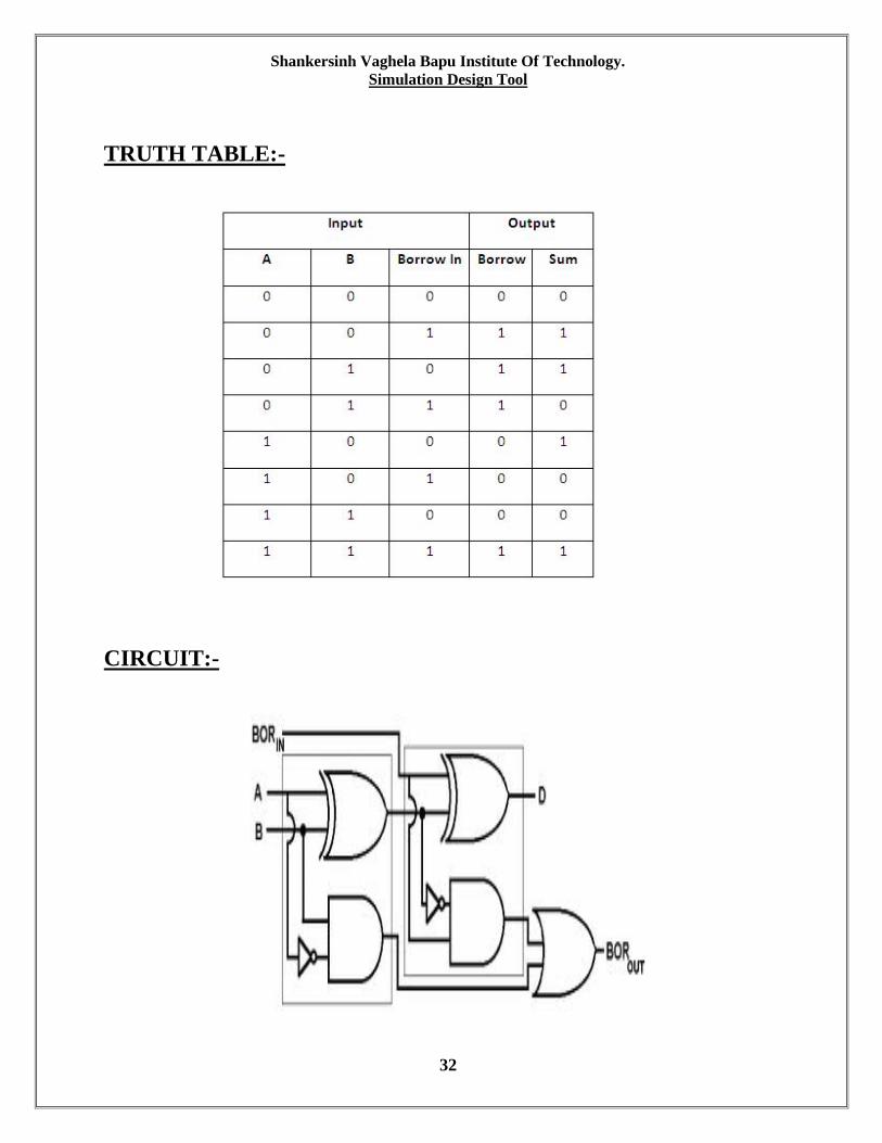
This circuit is performing binary subtraction of B from A (A-B,
recalling that in binary 0-1 = 1 borrow 1). Such a circuit is called a half-
subtractor, the reason for this is that it enables a borrow out of the
current arithmetic operation but no borrow in from a previous arithmetic
operation.
As in the case of the addition using logic gates, a full subtractor is
made by combining two half-subtractor and an additional OR-gate. A full
subtractor has the borrow in capability (denoted as BORIN in the diagram
below) and so allows cascading which results in the possibility of multi-
bit subtraction. The circuit diagram for a full subtractor is given below.
Shankersinh Vaghela Bapu Institute Of Technology.
Simulation Design Tool
32
TRUTH TABLE:-
CIRCUIT:-
Shankersinh Vaghela Bapu Institute Of Technology.
Simulation Design Tool
33
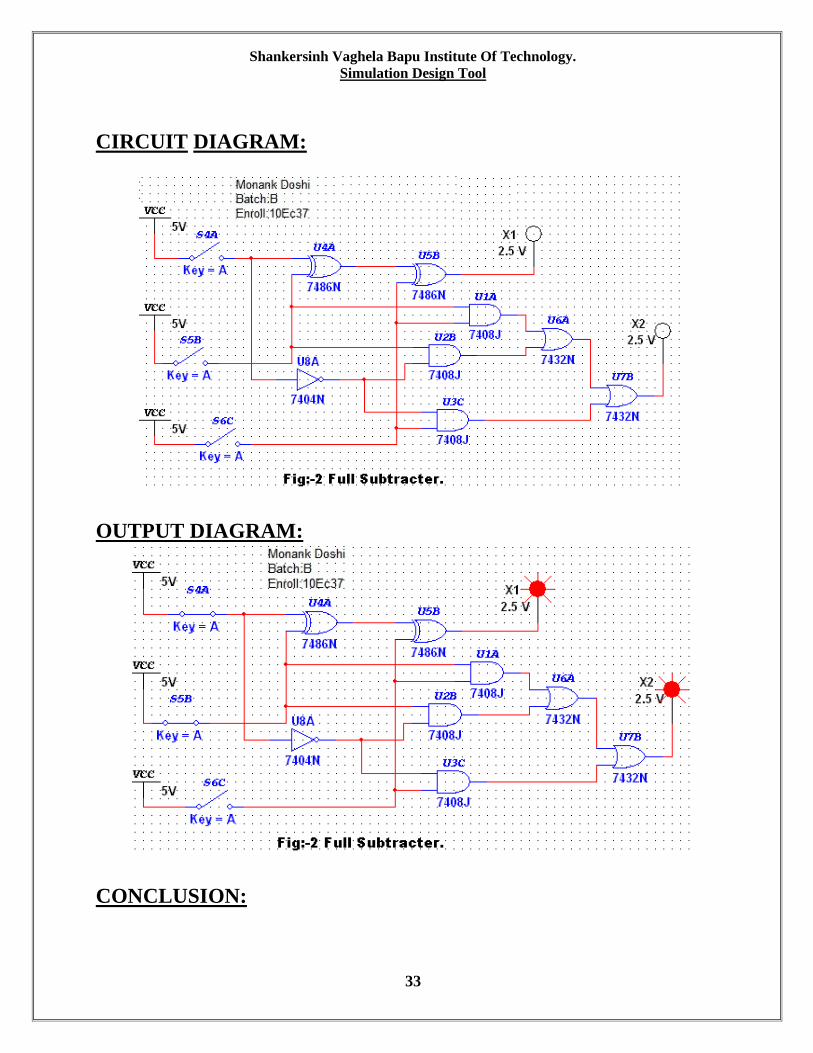
CIRCUIT DIAGRAM:
OUTPUT DIAGRAM:
CONCLUSION:
Shankersinh Vaghela Bapu Institute Of Technology.
Simulation Design Tool
34
EXPERIMENT:- 8
AIM:
Stimulate 3bit Synchronous UP Counter using Multisim and
determine its truth table.
EQUIPMENTS:
[1]. JK-FLIP FLOP.
[2]. AND GATE.
[3].CLOCK.
[4].OSCILLOSCOPE.
[5].VOLTAGE SOURCE.
THEORY:
A counter is a register capable of counting numbers of clock pulse
arriving at its clock input. Counter represents the number of clock pulses
arrived. An up/down counter is one that is capable of progressing in
increasing order or decreasing order through a certain sequence. An
up/down counter is also called bidirectional counter. Usually up/down
operation is controlled by up/down signal. When this signal is high
counter goes through up sequence and when up/down signal is low
counter follows reverse sequence. Here we are performing our exp using
3-bit up synchronous counter.
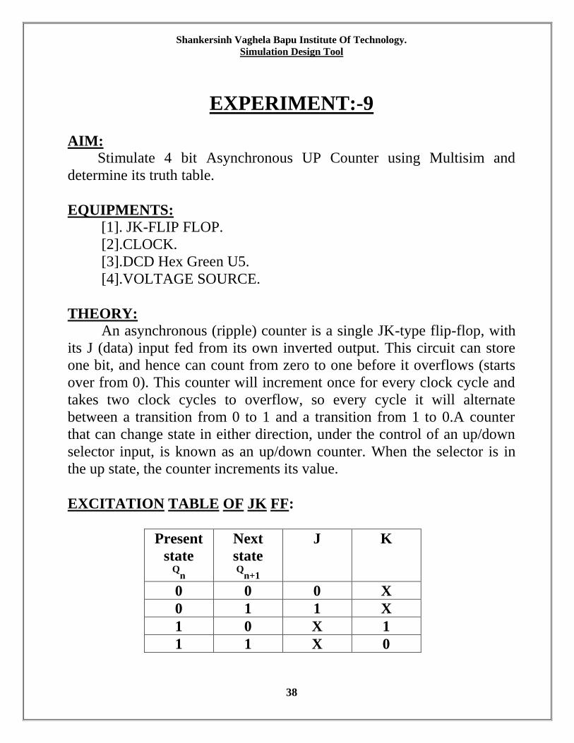
EXCITATION TABLE OF JK FF:
Present
state Q
n
Next
state Q
n+1
J K
0 0 0 X
0 1 1 X
1 0 X 1
1 1 X 0
Shankersinh Vaghela Bapu Institute Of Technology.
Simulation Design Tool
35
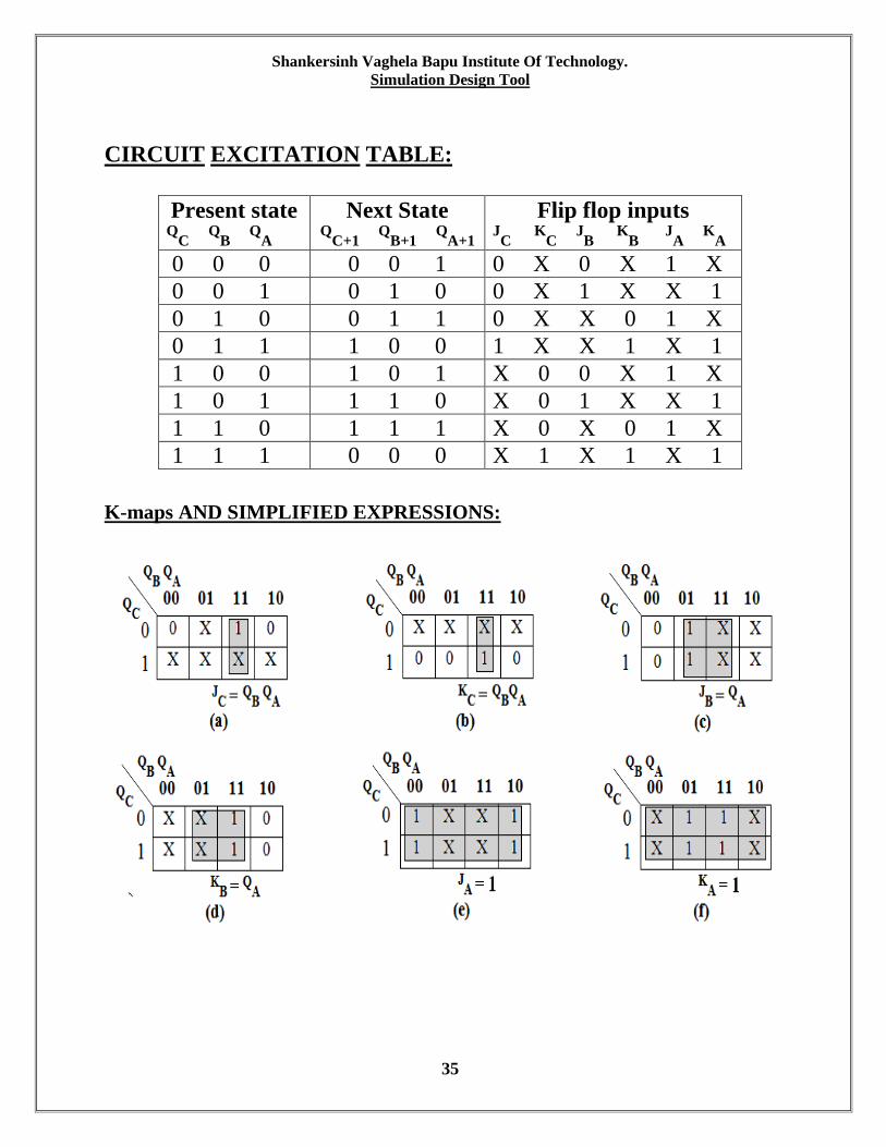
CIRCUIT EXCITATION TABLE:
K-maps AND SIMPLIFIED EXPRESSIONS:
Present state Q
C Q
B Q
A
Next State Q
C+1 Q
B+1 Q
A+1
Flip flop inputs JC
KC
JB
KB
JA
KA
0 0 0 0 0 1 0 X 0 X 1 X
0 0 1 0 1 0 0 X 1 X X 1
0 1 0 0 1 1 0 X X 0 1 X
0 1 1 1 0 0 1 X X 1 X 1
1 0 0 1 0 1 X 0 0 X 1 X
1 0 1 1 1 0 X 0 1 X X 1
1 1 0 1 1 1 X 0 X 0 1 X
1 1 1 0 0 0 X 1 X 1 X 1
Shankersinh Vaghela Bapu Institute Of Technology.
Simulation Design Tool
36
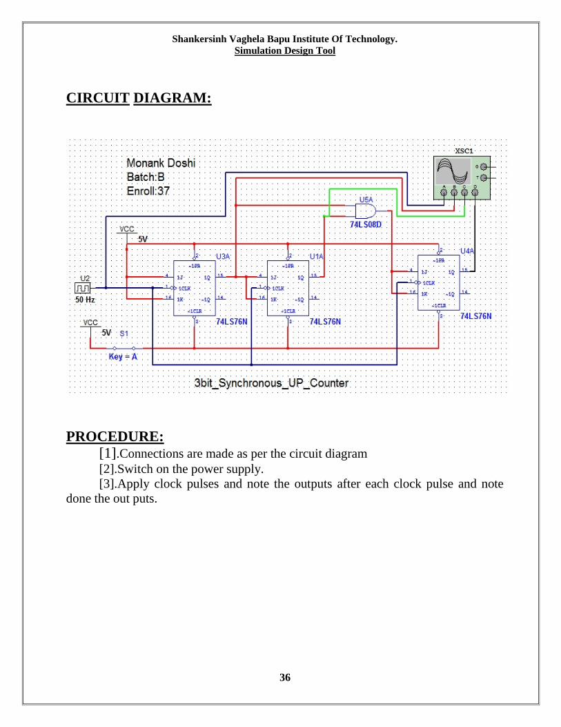
CIRCUIT DIAGRAM:
PROCEDURE:
[1].Connections are made as per the circuit diagram [2].Switch on the power supply.
[3].Apply clock pulses and note the outputs after each clock pulse and note
done the out puts.
Shankersinh Vaghela Bapu Institute Of Technology.
Simulation Design Tool
37
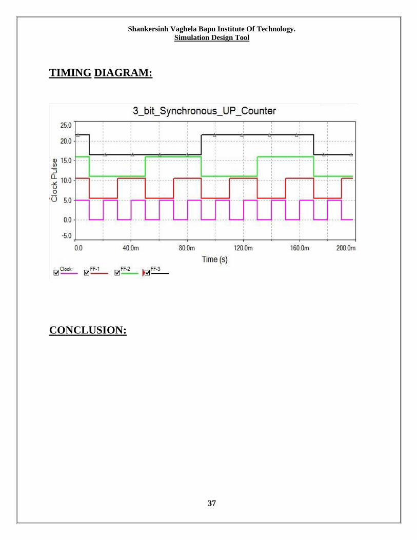
TIMING DIAGRAM:
CONCLUSION:
Shankersinh Vaghela Bapu Institute Of Technology.
Simulation Design Tool
38
EXPERIMENT:-9
AIM:
Stimulate 4 bit Asynchronous UP Counter using Multisim and
determine its truth table.
EQUIPMENTS:
[1]. JK-FLIP FLOP.
[2].CLOCK.
[3].DCD Hex Green U5.
[4].VOLTAGE SOURCE.
THEORY:
An asynchronous (ripple) counter is a single JK-type flip-flop, with
its J (data) input fed from its own inverted output. This circuit can store
one bit, and hence can count from zero to one before it overflows (starts
over from 0). This counter will increment once for every clock cycle and
takes two clock cycles to overflow, so every cycle it will alternate
between a transition from 0 to 1 and a transition from 1 to 0.A counter
that can change state in either direction, under the control of an up/down
selector input, is known as an up/down counter. When the selector is in
the up state, the counter increments its value.
EXCITATION TABLE OF JK FF:
Present
state Q
n
Next
state Q
n+1
J K
0 0 0 X
0 1 1 X
1 0 X 1
1 1 X 0

Shankersinh Vaghela Bapu Institute Of Technology.
Simulation Design Tool
39
CIRCUIT EXCITATION TABLE:
Present state Q
D Q
C Q
B Q
A
Next State Q
D+1 Q
C+1 Q
B+1 Q
A+1
Flip flop inputs JD
KD
JC
KC
JB
KB
JA
KA
0 0 0 0 0 0 0 1 0 X 0 X 0 X 1 X
0 0 0 1 0 0 1 0 0 X 0 X 1 X X 1
0 0 1 0 0 0 1 1 0 X 0 X X 0 1 X
0 0 1 1 0 1 0 0 0 X 1 X X 1 X 1
0 1 0 0 0 1 0 1 0 X X 0 0 X 1 X
0 1 0 1 0 1 1 0 0 X X 0 1 X X 1
0 1 1 0 0 1 1 1 0 X X 0 X 0 1 X
0 1 1 1 1 0 0 0 1 X X 1 X 1 X 1
1 0 0 0 1 0 0 1 X 0 0 X 0 X 1 X
1 0 0 1 1 0 1 0 X 0 0 X 1 X X 1
1 0 1 0 1 0 1 1 X 0 0 X X 0 1 X
1 0 1 1 1 1 0 0 X 0 1 X X 1 X 1
1 1 0 0 1 1 0 1 X 0 X 0 0 X 1 X
1 1 0 1 1 1 1 0 X 0 X 0 1 X X 1
1 1 1 0 1 1 1 1 X 0 X 0 X 0 1 X
1 1 1 1 0 0 0 0 X 1 X 1 X 1 X 1

Shankersinh Vaghela Bapu Institute Of Technology.
Simulation Design Tool
40
K-maps AND SIMPLIFIED EXPRESSIONS:
Shankersinh Vaghela Bapu Institute Of Technology.
Simulation Design Tool
41
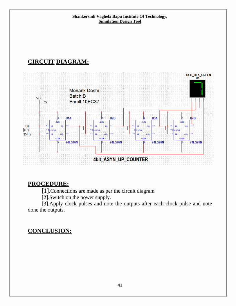
CIRCUIT DIAGRAM:
PROCEDURE:
[1].Connections are made as per the circuit diagram [2].Switch on the power supply.
[3].Apply clock pulses and note the outputs after each clock pulse and note
done the outputs.
CONCLUSION:
Shankersinh Vaghela Bapu Institute Of Technology.
Simulation Design Tool
42
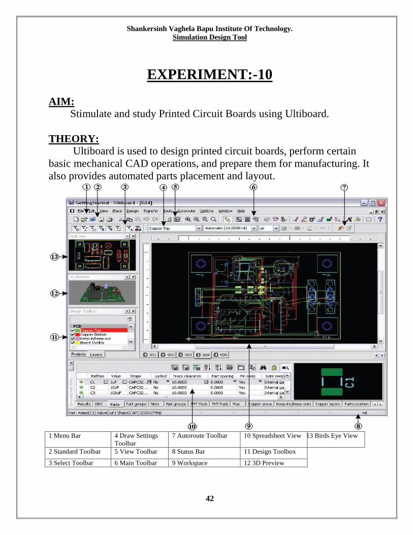
EXPERIMENT:-10
AIM:
Stimulate and study Printed Circuit Boards using Ultiboard.
THEORY:
Ultiboard is used to design printed circuit boards, perform certain
basic mechanical CAD operations, and prepare them for manufacturing. It
also provides automated parts placement and layout.
1 Menu Bar 4 Draw Settings
Toolbar
7 Autoroute Toolbar 10 Spreadsheet View 13 Birds Eye View
2 Standard Toolbar 5 View Toolbar 8 Status Bar 11 Design Toolbox
3 Select Toolbar 6 Main Toolbar 9 Workspace 12 3D Preview

Shankersinh Vaghela Bapu Institute Of Technology.
Simulation Design Tool
43
Design Toolbox:
Use the Design Toolbox, shown in the figure below, to manage
your design by controlling major parts of Ultiboard’s functionality.
The Design Toolbox is made up of two tabs:
The Projects tab is where you view the projects that are currently
open. Each project may contain one or more designs. Double-click
on a particular design to make it the active view.
The Layers tab is where you move between layers of your design,
control the appearance of layers, and perform several other
functions.
Autoroute Toolbar:
The Autoroute toolbar contains the autorouting and placement
functions supported by Ultiboard.
APPLICATIONS:
NI Ultiboard software helps students learn about the layout process
and industry practices by providing a flexible environment for PCB
layout and routing.
Students can retrieve designs from NI Multisim interactive SPICE-
based simulation or begin from scratch using parts from the built-in
Ultiboard database of land patterns.
Main features: - Prepares students for professional design
activities with integrated layout and routing.
Combine with NI Multisim to simplify transfer of designs from
schematic to layout.
Helps students produce their first PCBs with pick-and-place
components and follow-me routing.
Exports to standard formats including Gerber to give students an
understanding of industry practices.
Creates designs of up to four layers with up to 1,000 pin.

Shankersinh Vaghela Bapu Institute Of Technology.
Simulation Design Tool
44
CIRCUIT DIAGRAM:
PCB DESIGN:
CONCLUSION: