
Simulation and Analysis of Methylammonium Lead Iodide 3NH...
8
American Journal of Optics and Photonics 2019; 7(2): 33-40 http://www.sciencepublishinggroup.com/j/ajop doi: 10.11648/j.ajop.20190702.12 ISSN: 2330-8486 (Print); ISSN: 2330-8494 (Online) Simulation and Analysis of Methylammonium Lead Iodide (CH 3 NH 3 PbI 3 ) Perovskite Solar Cell with Au Contact Using SCAPS 1D Simulator Ali Husainat 1, * , Warsame Ali 2 , Penrose Cofie 2 , John Attia 2 , John Fuller 2 1 Department of Electrical and Computer Engineering, Prairie View A&M University, Prairie View, USA 2 Department of Electrical and Computer Engineering, Faculty of Electrical Engineering, Prairie View A&M University, Prairie View, USA Email address: * Corresponding author To cite this article: Ali Husainat, Warsame Ali, Penrose Cofie, John Attia, John Fuller. Simulation and Analysis of Methylammonium Lead Iodide (CH 3 NH 3 PbI 3 ) Perovskite Solar Cell with Au Contact Using SCAPS 1D Simulator. American Journal of Optics and Photonics. Vol. 7, No. 2, 2019, pp. 33-40. doi: 10.11648/j.ajop.20190702.12 Received: July 17, 2019; Accepted: August 10, 2019; Published: August 20, 2019 Abstract: Hybrid organic-inorganic perovskite solar cells have attracted the attention of researchers and scientists throughout the world. From 2009, when actual research work began on photovoltaic perovskite applications, a lab power conversion efficiency above 23.3% have been achieved. Whereas, silicon solar cells have only achieved power conversion efficiencies around 17.5% in both residential and commercial applications. A typical perovskite solar cell consists of 6 main layers of different materials: a glass layer, a thin layer of fluorine-doped tin oxide substrate (FTO), an electron transport layer of TiO 2 , a perovskite active layer known as methylammonium lead iodide (CH 3 NH 3 PbI 3 ), a hole transport layer of Spiro- Ometad, and a gold (Au) electrode. This paper summarizes the research that focused on the selective use of the perovskite solar cell’s composite materials, specifically, the Spiro-Ometad layer, the methylammonium lead iodide layer (CH 3 NH 3 PbI 3 ), and the TiO 2 layer with a variation of the thickness of the perovskite layer. Initial simulation results show a power conversion efficiency of 20.34% when using a gold (Au) electrode. Further research is needed, in which new technology for device fabrication will create homogeneous thin-film layers that will be tested for increased efficiency. Keywords: Modeling, Simulation, Perovskite Solar Cell, Photovoltaics, Inorganic Materials, Organic Materials 1. Introduction Until now, the silicon solar cell has an efficiency in the range of 12-17.5% PCE, which lead to an extensive search for a new material with better efficiency. Thus, researchers started looking into hybrid materials for photovoltaic applications. Hybrid photovoltaic technology is an emerging field, compared with inorganic silicon solar cells. Since the 1950s, silicon materials used as the primary material in making solar cells. Hybrid organic-inorganic perovskite solar cells have gained special attention since 2009, with exponential efficiency increases from 3.8% to 23.3% PCE. Perovskite solar cells offer a compelling combination of extremely low-cost, ease of fabrication, and high device performance [1, 2]. The perovskite solar cell (PSC) has the optical and electrical property to absorb not only the visible light spectrum but also the near-infrared as well. In contrast, the silicon solar cell can only absorb the visible light spectrum. Furthermore, the perovskite solar cell has passed the 23.0% PCE, which makes it an excellent and more efficient alternative to silicon. In this study, we have used a simulation program called Solar cell capacitance simulator (SCAPS) 1D. To model the perovskite solar cell, we used real experiment data in the simulator to analyze the perovskite solar cell. We have also examined the effect of the absorber layer thickness, doping concentrations, and defects on the performance of the solar cell performance [1].
Transcript of Simulation and Analysis of Methylammonium Lead Iodide 3NH...
American Journal of Optics and Photonics 2019; 7(2): 33-40
http://www.sciencepublishinggroup.com/j/ajop
doi: 10.11648/j.ajop.20190702.12
ISSN: 2330-8486 (Print); ISSN: 2330-8494 (Online)
Simulation and Analysis of Methylammonium Lead Iodide (CH3NH3PbI3) Perovskite Solar Cell with Au Contact Using SCAPS 1D Simulator
Ali Husainat1, *
, Warsame Ali2, Penrose Cofie
2, John Attia
2, John Fuller
2
1Department of Electrical and Computer Engineering, Prairie View A&M University, Prairie View, USA 2Department of Electrical and Computer Engineering, Faculty of Electrical Engineering, Prairie View A&M University, Prairie View, USA
Email address:
*Corresponding author
To cite this article: Ali Husainat, Warsame Ali, Penrose Cofie, John Attia, John Fuller. Simulation and Analysis of Methylammonium Lead Iodide
(CH3NH3PbI3) Perovskite Solar Cell with Au Contact Using SCAPS 1D Simulator. American Journal of Optics and Photonics.
Vol. 7, No. 2, 2019, pp. 33-40. doi: 10.11648/j.ajop.20190702.12
Received: July 17, 2019; Accepted: August 10, 2019; Published: August 20, 2019
Abstract: Hybrid organic-inorganic perovskite solar cells have attracted the attention of researchers and scientists
throughout the world. From 2009, when actual research work began on photovoltaic perovskite applications, a lab power
conversion efficiency above 23.3% have been achieved. Whereas, silicon solar cells have only achieved power conversion
efficiencies around 17.5% in both residential and commercial applications. A typical perovskite solar cell consists of 6 main
layers of different materials: a glass layer, a thin layer of fluorine-doped tin oxide substrate (FTO), an electron transport layer
of TiO2, a perovskite active layer known as methylammonium lead iodide (CH3NH3PbI3), a hole transport layer of Spiro-
Ometad, and a gold (Au) electrode. This paper summarizes the research that focused on the selective use of the perovskite
solar cell’s composite materials, specifically, the Spiro-Ometad layer, the methylammonium lead iodide layer (CH3NH3PbI3),
and the TiO2 layer with a variation of the thickness of the perovskite layer. Initial simulation results show a power conversion
efficiency of 20.34% when using a gold (Au) electrode. Further research is needed, in which new technology for device
fabrication will create homogeneous thin-film layers that will be tested for increased efficiency.
Keywords: Modeling, Simulation, Perovskite Solar Cell, Photovoltaics, Inorganic Materials, Organic Materials
1. Introduction
Until now, the silicon solar cell has an efficiency in the
range of 12-17.5% PCE, which lead to an extensive search
for a new material with better efficiency. Thus, researchers
started looking into hybrid materials for photovoltaic
applications. Hybrid photovoltaic technology is an
emerging field, compared with inorganic silicon solar cells.
Since the 1950s, silicon materials used as the primary
material in making solar cells. Hybrid organic-inorganic
perovskite solar cells have gained special attention since
2009, with exponential efficiency increases from 3.8% to
23.3% PCE. Perovskite solar cells offer a compelling
combination of extremely low-cost, ease of fabrication, and
high device performance [1, 2]. The perovskite solar cell
(PSC) has the optical and electrical property to absorb not
only the visible light spectrum but also the near-infrared as
well.
In contrast, the silicon solar cell can only absorb the
visible light spectrum. Furthermore, the perovskite solar
cell has passed the 23.0% PCE, which makes it an excellent
and more efficient alternative to silicon. In this study, we
have used a simulation program called Solar cell
capacitance simulator (SCAPS) 1D. To model the
perovskite solar cell, we used real experiment data in the
simulator to analyze the perovskite solar cell. We have also
examined the effect of the absorber layer thickness, doping
concentrations, and defects on the performance of the solar
cell performance [1].

American Journal of Optics and Photonics 2019; 7(2): 33-40 34
2. Perovskite Structure
Any material that has a similar crystal structure to the
mineral CaTiO3 (Figure 1 and Figure 2) at a different
transition state is called perovskite. The formula ABX3
represents the perovskite crystal structure (Figure 5), where
A is a large organic or inorganic cation, B is a smaller
inorganic cation such as (Cu2+, Sn2+, Pb2+) [4, 5], and X3 is
an ion from the halogen group (such as Cl-, Br- and I-) that is
able to bond with both cations A and B [1]. There are two
main categories of perovskite crystal structure and can be
classified into 1) Haloalkanes perovskite and 2) organic-
inorganic halide perovskite. Perovskite materials have
excellent optoelectronic behavior, which makes them
function well as the absorber layer for photovoltaic
application, this is the result of their having high absorption
coefficients, making them a more efficient alternative to
silicon. Another important characteristic is their ferroelectric
behavior, which was discovered half a century ago.
Figure 1. Same as Figure 2, but different view: Many ABX3 compounds adopt the perovskite structure, with A ions occupying large, 12-fold coordinated sites;
B ions are in octahedral coordination by X.
Figure 2. CaTiO3 Perovskite - TETRAGONAL phase: each titanium atom bonds to six nearest-neighbor oxygen atoms.
Perovskite has a direct bandgap of Eg between 1.3 to 2.2
eV, which gives it the optical properties necessary to harvest
and convert near-infrared (NIR) and ultraviolet (UV) light
into visible light, which can then be utilized by the perovskite
active layer as shown in Figure 3 [5-7].
In the 1990s, scientists discovered that halide perovskite
could convert light into electricity. Due to this discovery, the
light-emitting diodes (LED) were made. Perovskite structure
has four possible phases, such as 1) α is cubic structure phase
occurs at T > 327 K. 2) β is a tetragonal structure phase
occurs at T< 327° K, 3) γ is orthorhombic structure phase
occurs at T=160° K. 4) δ is a polyhedral phase structure
which is a none perovskite phase [8, 9].

35 Ali Husainat et al.: Simulation and Analysis of Methylammonium Lead Iodide (CH3NH3PbI3) Perovskite
Solar Cell with Au Contact Using SCAPS 1D Simulator
Figure 3. Standard solar spectral (source PVeducation. com).
The tolerance factor giving by equation (1):
� � �������√�������
(1)
In order to maintain the cubic structure of the perovskite
layer, the tolerance factor should be close to one, where, RA,
RB, and RX are the radius of the ions. In order to have a
stable perovskite, the tolerance factor must be in the range
of 0.7< T < 1, which maintain and hold the bond between
both cations. Cation A >> cation B to have a stable
perovskite structure. Therefore, Methylammonium (MA+)
ion is one of the best organic material options. The
transformation of perovskite depends on the tilting and
rotation of BX6 [6-8].
Figure 4. Cubic structure of MAPbI3 with symmetrical distant between MA-MA, Pb-I atoms.
From 2013 to about mid of 2018, referenced studies [10-12]
reported 15.6%, 15.9%, 16.7%, 19.3%, 20.1%, 22.1% and 22.7%
PCE respectively. We can see that the PCE of the perovskite solar
cell increased very rapidly, as shown in Figure 5.
This comparison makes the perovskite a promising
candidate. The primary goal of designing a highly efficient
solar cell is to optimize the power conversion efficiency
(PCE) to cost ratio. Furthermore, and due to this rapid
research and improvement of the perovskite family,
MAPbBr3, MAPbCl3, and MAPbI3. Methylammonium lead
iodide (MAPbI3) is the one that proved to be the best
perovskite material due to its excellent electrical and optical
properties, low-temperature solution processability, long
lifetime, and ferroelectricity. The efficiency of the perovskite
solar cell can be further improved through different design
techniques to not only the absorber layer but to all other six
layers, as shown in Figure 6 [13].
Figure 5. Comparison of the lab efficiencies of Silicon and Perovskite over the years. (source: metSolar. eu).

American Journal of Optics and Photonics 2019; 7(2): 33-40 36
Figure 6. Perovskite solar cell normal setup.
Figure 7. Energy Levels of the Device Layers.
Figure 7 shows the energy levels of the device Layers; it
must be in this position for an easy transfer of the electrons
and holes through their transport layers to the electrodes.
3. Experimental Details: Simulation and
Analysis Approach of Perovskite Solar
Cells
Simulation can show the physical operation, the viability
of a proposed physical model and is an important way of
understanding the device operation, and how the device
parameters affect the physical operation and performance of
the solar cell devices instantly without the need to wait for
long or spend money prior seen a result. There are various
simulation models used throughout the photovoltaics
technology (AMPS, COMSOL MULTIPHYSICS, GPVDM,
SCAPS, SILVACO, and TCAD). In this paper, we use
SCAPS 1D simulator to model the perovskite-based solar
cells [14] we can define up to 7 semiconductor layers.
SCAPS 1D can be used to simulate PSC because it has a very
intuitive operation window diversified models for grading,
defects, recombination, and generation. Once all parameters
defined, it behaves like a real-life counterpart. The following
differential equations in one dimension, are applied:
� ������ �
�ℇ [���� − ���� − ������ +
������ − ����� + �����] (2)
Poisson’s Equation
� ," � �#$ % + #& �+
�#$'% − #&' ' � (3)
Transport equations
( ," � )& ,"* ," (4)
Diffusion Length
& ," � [+,�-� . $ ," (5)
Diffusivity
," � � /
� 01 � + �2 − 3 � + /�
04 � + �2" − 3"� (6)
Continuity equation
567 � ,�-� [8� +9:9; + 1.] (7)
Where �: is the electrostatic potential, q is an elementary
charge, ℇ is the permittivity, n is the density of free electron,
p is the density of free hole, ��� is the ionized donor (doping
density), ��� is the ionized acceptor (doping density),
�� >?�ℎA�BC��ADℎEFADA�?>�G, �� is the electron trapped
density, Ln, p is the diffusion length of electron and holes,
& ,">?�ℎAAFAH�BE�, ℎEFA&>IIJ?>K>�G , $ is the electron
mobility, * is the electron lifetime, n, p is the electron/hole
concentration, E is the electric field, ," � is the concentration
gradient for the electrons/holes, 2 ," is the optical generation
rate, 3 ," is the recombination rate [15, 16], Voc is the open-
circuit voltage, � is the ideality factor, LBM⁄# is the thermal
voltage, 8( is the solar cell light generated current, and 80 is
the reverse saturation current.
PSC used in the simulation is an n-i-p structure laid
between the n-type semiconductor Titanium Oxide (TiO2) as
an Electron Transport Layer (ETL) and p-type Spiro-
OMeTAD as a Hole Transport Layer (HTL). A SnO2: F as
Fluorine doped Tin Oxide (FTO) is the transparent
conductive oxide (TCO), and Au (Gold) as conductor Figure
6 [17, 18]. Solar Cell Capacitance Simulator (SCAPS) is
used to simulate PSCs. SCAPS -1D is one of the most widely
used device simulators in inorganic solar cells. The simulator
uses the three main differential equations 1) Poisson’s
equation, 2) transport equation, and 3) continuity equation,
which is developed by a group of researchers at the
University of Gent, Belgium.
37 Ali Husainat et al.: Simulation and Analysis of Methylammonium Lead Iodide (CH3NH3PbI3) Perovskite
Solar Cell with Au Contact Using SCAPS 1D Simulator
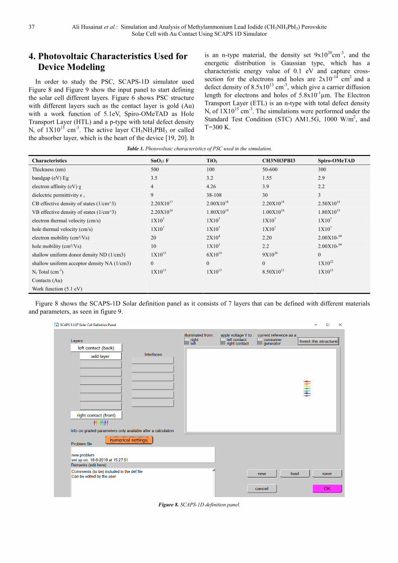
4. Photovoltaic Characteristics Used for
Device Modeling
In order to study the PSC, SCAPS-1D simulator used
Figure 8 and Figure 9 show the input panel to start defining
the solar cell different layers. Figure 6 shows PSC structure
with different layers such as the contact layer is gold (Au)
with a work function of 5.1eV, Spiro-OMeTAD as Hole
Transport Layer (HTL) and a p-type with total defect density
Nt of 1X10¹⁵
cm-3
. The active layer CH3NH3PBI3 or called
the absorber layer, which is the heart of the device [19, 20]. It
is an n-type material, the density set 9x10²⁰
cm-3
, and the
energetic distribution is Gaussian type, which has a
characteristic energy value of 0.1 eV and capture cross-
section for the electrons and holes are 2x10-14
cm2
and a
defect density of 8.5x10¹³
cm-3
, which give a carrier diffusion
length for electrons and holes of 5.8x10⁻¹
µm. The Electron
Transport Layer (ETL) is an n-type with total defect density
Nt of 1X10¹⁵
cm-3
. The simulations were performed under the
Standard Test Condition (STC) AM1.5G, 1000 W/m2, and
T=300 K.
Table 1. Photovoltaic characteristics of PSC used in the simulation.
Characteristics SnO2: F TiO2 CH3NH3PBI3 Spiro-OMeTAD
Thickness (nm) 500 100 50-600 300
bandgap (eV) Eg 3.5 3.2 1.55 2.9
electron affinity (eV) χ 4 4.26 3.9 2.2
dielectric permittivity Nr 9 38-108 30 3
CB effective density of states (1/cm^3) 2.20X10¹⁷ 2.00X10¹⁸ 2.20X10¹⁸ 2.50X10¹⁸
VB effective density of states (1/cm^3) 2.20X10¹⁶ 1.80X10¹⁹ 1.00X10¹⁸ 1.80X10¹⁹
electron thermal velocity (cm/s) 1X10⁷ 1X10⁷ 1X10⁷ 1X10⁷
hole thermal velocity (cm/s) 1X10⁷ 1X10⁷ 1X10⁷ 1X10⁷
electron mobility (cm²/Vs) 20 2X10⁴ 2.20 2.00X10-04
hole mobility (cm²/Vs) 10 1X10³ 2.2 2.00X10-04
shallow uniform donor density ND (1/cm3) 1X10¹⁵ 6X10¹⁹ 9X10²⁰ 0
shallow uniform acceptor density NA (1/cm3) 0 0 0 1X10²²
Nt Total (cm-3) 1X10¹⁵ 1X10¹⁵ 8.50X10¹³ 1X10¹⁵
Contacts (Au)
Work function (5.1 eV)
Figure 8 shows the SCAPS-1D Solar definition panel as it consists of 7 layers that can be defined with different materials
and parameters, as seen in figure 9.
Figure 8. SCAPS-1D definition panel.

American Journal of Optics and Photonics 2019; 7(2): 33-40 38
Figure 9. SCAPS-1D definition panel with PSC cell Layers name.
Figure 10. I-V characteristics curve of PSC with Au contacts.
5. Results and Discussion
In this study, we observed the thickness of the absorber
layer, which has a very high absorption coefficient up to
105cm-1
. It is a very critical parameter that affects the PSC
performance, and it is electrical properties such as (Jsc, Voc,
FF, and PCE), the short-circuit current density, the open-
circuit voltage, Fill Factor and the power conversion
efficiency, respectively. As the absorber thickness (vary from
50 to 600 nm). The default parameters for the other layers set,
as mentioned in Table 1. As shown in Figure 10, which
shows the optimal cell performance around the thickness of
300nm for the active layer, and then decreases slightly.
While Voc increases to an optimal value at 200nm and then
decreases afterward. For fill factor, it increases slowly when
the thickness increases. The behavior of the efficiency is very
similar to Voc, increasing to an optimal value between
300nm and 400nm, and then decreases with the thickness
increase. Another important property is the charge carriers in
the perovskite active layer has a longer diffusion length than
300nm as the case of our model, where the electron and hole
can reach their corresponding electrode before they
recombine, which can enhance the efficiency [21].
Moreover, Voc is defined by equation (8). More excess
carrier’s concentration gives a higher value of IL, while I0
stays at a low level because of not much recombination in the
cell. This is the reason why Voc increases for the first time.
Fill Factor is defined as the ratio of the maximum generated
power to the product of Voc and Isc when the thickness is
less than 500nm. However, the PCE is increasing with the
thickness increases to some degree. The internal power
depletion is also increasing after 300 nm. While the thickness
of more than 300 nm, we start noticing the decreasing effect
on the PCE, which caused by more recombination happens
because of the increasing number of traps and because more
and more excess carriers cannot reach the electrodes. In this
case, thicker absorber brings drops of Voc and PCE. In this
simulation, the performance of a solar cell is dominated by
two factors, 1) How efficient is the active layer can absorb
the photon. 2) How fast the charge carrier can move to the
corresponding electrode [22, 23].

39 Ali Husainat et al.: Simulation and Analysis of Methylammonium Lead Iodide (CH3NH3PbI3) Perovskite
Solar Cell with Au Contact Using SCAPS 1D Simulator
6. Conclusion
We employed the device simulator SCAPS 1D in the
modeling of PSC. SCAPS-1D [24] simulator. The
researchers widely use this program from around the world
for modeling all type of solar cell. We have Au as a contact
layer with a work function of 5.1eV, Spiro-Ometad,
CH3NH3PBI3 as an absorber layer with a different thickness
between 50nm to 600nm, the results are shown in Table 2.
Figure10 shows a 300nm thickness is an optimal thickness
for the absorber with an efficiency of 20.34%, and TiO2 as
ETL.
Table 2. Shows the simulation results.
Thickness (nm) Voc (V) Jsc (mA/cm2) FF% Efficiency %
50 1.4551 5.936405 89 7.7
100 1.471 9.708584 90 12.85
200 1.4772 13.804484 91 18.49
300 1.4758 15.158235 91 20.34
400 1.4726 15.042101 91 20.16
500 1.4689 14.159126 91 18.93
600 1.4652 12.912388 91 17.22
Acknowledgements
We would like to thank Dr. Marc Burgelman and his staff,
at the University of Gent, Belgium, for the freely distributed
SCAPS-1D simulator.
References
[1] Frost JM, Butler KT, Brivio F, Hendon CH, Schilfgaarde MV, and Walsh A. Atomistic origin of high performance in. Hybrid halide perovskite solar cells. Nano Lett. 2014; 14: 2484-2590.
[2] Baikie T, Fang YN, Kadro JM, Schreyer M, Wei FX, Mhaisalkar SG, Gratzel M, and White TJ "Synthesis And Crystal Chemistry Of The Hybrid Perovskite". https://pubs.rsc.org/en/content/articlelanding/2013/ta/c3ta10518k sensitized solar cell applications. J. Mater. Chem. A. 2013; 1: 5628–5641.
[3] Stoumpos C, Malliakas CD, and Kanatzidis MG."Thermochromic Halide Perovskite Solar Cells |Nature materials." https://www.nature.com/articles/s41563-017-0006-2013; 52: 9019–9038.
[4] "Synthesis And crystal Chemistry Of The Hybrid Perovskite"https://pubs.rsc.org/en/content/articlelanding/2013/ta/c3ta10518k.
[5] Yin WJ, Yang JH, Kang J, Yan Y, and Wei SH. Halide perovskite materials for Solar cells: a theoretical review. J. Mater. Chem. A. 2014.
[6] Walsh A, Watson GW. The origin of the stereochemically active Pb (II) lone Pair: DFT calculations on PbO and PbS. Journal of Solid-State Chemistry. 2005; 178: 1422–1428.
[7] Walsh A, Payne DJ, Egdell RG, and Watson GW. Stereochemistry of post-Transition metal oxides: revision of the classical lone pair model. Chem. Soc. Rev. 2011; 40: 4455 446.
[8] Keith T. Butler, Jarvis M. Frost, and Aron Walsh, Band alignment of the hybrid Halide perovskites CH3NH3PbCl3, CH3NH3PbBr3, and CH3NH3PbI3. Materials Horizons. 2014; 2: 228-231.
[9] Gray, D. E. American Institute of Physics Handbook, 3rd ed.; McGraw-Hill: New York, 1982.
[10] Lide, D. R. CRC Handbook of Chemistry and Physics, 73rd ed; CRC Press: Boca Raton, FL, 1994.
[11] Stranks, S. D.; Eperon, G. E.; Grancini, G.; Menelaou, C.; Alcocer, M. J. P.; Leijtens, T.; Herz, L. M.; Petrozza, A.; Snaith, H. J. Electron-Hole Diffusion Lengths Exceeding Micrometer in an Organometal Trihalide Perovskite Absorber. Science 2013, 342, 341−344.
[12] Lee MM, Teuscher J, Miyasaka T, Murakami TN, and Snaith HJ. Efficient hybrid Solar cells based on meso- superstructure organometal halide perovskites. Science. 2012; 338: 643-647.
[13] "Strong-Covalency-induced-Recombination-CentersIn..." http://pubs.acs.org/doi/abs/10.1021/ja5079305.26May. 2019.
[14] Liu F, Zhu J, Wei J, Li Y, Li M, Yang S, Zhang B, Yao J, and Dai S. Numerical simulation: Toward the design of high-efficiency planar perovskite solar cells. Applied Physics Letters. 2014; 104: 253508.
[15] Walsh A, Watson GW. The origin of the stereochemically active Pb (II) lone pair: DFT calculations on PbO and PbS. Journal of Solid-State chemistry. 005; 178: 1422–1428.
[16] Miyasaka T, Kojima A, Teshima K, and Shirai Y. Organometal halide perovskite As a visible- light sensitizer for photovoltaic cells. Jour. of Americ. Chem. Soc. 2009; 131: 6050-6051.
[17] Walsh A, Payne DJ, Egdell RG, and Watson GW. Stereochemistry of post-transition metal oxides: revision of the classical lone pair model. Chem. Soc. Rev. 2011; 40: 4455–446.
[18] G. Haacke, the New figure of merit for transparent conductors, J. Appl. Phys. 47.
[19] Lee MM, Teuscher J, Miyasaka T, Murakami TN, and Snaith HJ. Efficient hybrid Solar cells based on meso-superstructure organometal halide perovskites. Science. 2012; 338: 643-647.
[20] Jeon NJ, Lee HG, Kim YC, Seo J, Noh JH, Lee J, and Seok SI. O-Methoxy Substituents in Spiro-OMeTAD for Efficient inorganic-organic Hybrid Perovskite Solar Cells. J. Am. Chem. Soc. 2014; 136: 7837−7840.
[21] Wang JT, Ball JM, Barea EM, Abate A, Alexander-Webber JA, Huang J, Saliba M, Mora-Sero I, Bisquert J, Snaith HJ, and Nicholas RJ. Low-temperature processed electron collection layers of graphene/TiO2 nanocomposites in thin film perovskite solarCells. Nano Letters. 2014; 14: 724-730.
[22] Wojciechowski K, Saliba M, Leijtens T, Abate A, and Snaith HJ. Sub-1500 C Processed meso-super structured perovskite solar cells with enhanced efficiency. Energy Environ Sci. 2014; 7: 1142-1147.
[23] Jeon NJ, Lee HG, Kim YC, Seo J, Noh JH, Lee J, and Seok SI. O-Methoxy SubstituentsIn Spiro-OMeTAD for Efficient organic−OrganicHybrid perovskite Solar Cells. J. Am. Chem. Soc. 2014; 136: 7837−7840.

American Journal of Optics and Photonics 2019; 7(2): 33-40 40
[24] Zhou H, Chen Q, Li G, Luo S, Song T, Duan HS, Hong Z, Yu J, Liu Y, Yang Y. Interface Engineering of highly efficient perovskite solar cells. Science. 2014; 345: 542546.
[25] Green MA, Emery K, Hishikawa Y, Warta W, and Dunlop ED. Solar cell efficiency tables (Version 45). Prog. Photovolt: res. Appl. 2015; 23: 1-9.


![A Smart Semi-Automated Multifarious Surveillance Bot for ...article.networksjournal.org/pdf/10.11648.j.net.20190702.12.pdf · surveillance [10-12]. Moreover, modern devices such as](https://static.fdocuments.in/doc/165x107/5f5d87ddfb2c0a53764aea9a/a-smart-semi-automated-multifarious-surveillance-bot-for-surveillance-10-12.jpg)