Simulating the Device Characteristics of MEH-PPV Polymer Light
4
May 2005 Page 5 The Simulation Standard Simulating the Device Characteristics of MEH-PPV Polymer Light Emitting Diodes Using ATLAS Introduction Organic light emitting diodes (OLEDs) are attracting great interest in the display technology industry due to their promising low cost large area manufacturing and relative ease of fabrication using low processing temperatures. Although the research work of OLEDs has began since early 1980 and has been well established, there is still no commercially available software that can simulate the electrical and optical behavior of these organic polymer/monomer based devices. As such, Silvaco-ATLAS - - has recently extended its capability to simulate these devices using a variety of appropriate organic polymer/monomer models. In this article, we will present the use of ATLAS in simu- lating OLEDs based upon the commonly used organic material i.e. MEH-PPV [more fully known as poly(2- methoxy,5-(2’-ethyl-hexoxy)-1,4-phenylenevinylene)]. MEH-PPV has been chosen in the paper since it has been an attractive material in OLED fabrication because of its solubility in common organic solvents, in conjunction with a low operating voltage for light emission and rela- tively high conversion efficiency [1]. Device Simulation Structure Figure 1 shows the simulation structure used in this pa- per. It is a three layer device; typically consisting of the MEH-PPV polymer film sandwiched between an Indium- Tin-Oxide (ITO) coated glass substrate and a metal. The ITO is the anode while the cathode is made up of metal. Whether these contacts are electron or hole injection lim- ited depends on their workfunction with respect to the LUMO and HOMO energy levels of the MEH-PPV. In this simulation, the thickness of both electrodes are set to 0.05μm while the thickness of the MEH-PPV will be varied between the range of 475Å to 2100Å so as to study the electrical characteristics of the OLED device. Models and Device Parameters In this organic polymer LED simulation, the Poole-Fren- kel-like mobility model and the Langevin bimolecular recombination model have been used as the transport and recombination mechanism. These models are enabled in ATLAS by specifying the parameters PFMOB and LAN- GEVIN in the MODEL statement. In addition, to infer the radiative rates for luminescence or phosphorescence due to the Langevin recombination in organic polymer LEDs, the distribution of singlet or triplet excitons has to be calculated. ATLAS has included the exciton rate equation which is self-consistently solved along with the electron and hole drift diffusion equations. To enable the self-con- sistent simulation of excitons, the EXCITON parameter was also included in the MODEL statement. For the Poole-Frenkel-like mobility model, additional pa- rameters such as the DELTAEN.PFMOB, DELTAEP.PFMOB, BETAN.PFMOB and BETAP.PFMOB, are specified in the MOBILITY statement. DELTAEN.PFMOB and DELTAEP.PFMOB are the thermal activation energy of the organic polymer at zero electric field for elec- trons and holes respectively while BETAN.PFMOB and BETAP.PFMOB are the electron and hole Poole-Frenkel factor respectively. The device material parameters used in this simulation are given in Table 1 Figure 1 Schematic diagram of the simulation structure. Table 1. Device parameters used in this simulation. Parameter Magnitude Units Bandgap energy, E g 2.1 eV Temperature, T 300 K Affinity 2.8 eV ITO Workfunction 4.7 eV Density of State, N 0 2.5 × 10 19 cm -3 Hole mobility, µ p 0.5 × 10 -4 cm 2 V -1 s -1 Electron mobility, µ n 0.5 × 10 -5 cm 2 V -1 s -1 Exciton lifetime, τ 1 × 10 -9 s Exciton diffusion length, L D 1 × 10 -6 cm Fraction of excitons formed 0.45 unitless as singlets, F Relative permittivity, ε r 3.0 unitless Richardson constant 120 A cm -2 K -2
Transcript of Simulating the Device Characteristics of MEH-PPV Polymer Light
The Simulation Standard Page 4 May 2005 May 2005 Page 5 The Simulation Standard
Simulating the Device Characteristics of MEH-PPV Polymer Light Emitting Diodes Using ATLAS
IntroductionOrganic light emitting diodes (OLEDs) are attracting great interest in the display technology industry due to their promising low cost large area manufacturing and relative ease of fabrication using low processing temperatures. Although the research work of OLEDs has began since early 1980 and has been well established, there is still no commercially available software that can simulate the electrical and optical behavior of these organic polymer/monomer based devices. As such, Silvaco-ATLAS Silvaco-ATLAS Silvaco- has recently extended its capability to simulate these devices using a variety of appropriate organic polymer/monomer models.
In this article, we will present the use of ATLAS in simu-lating OLEDs based upon the commonly used organic material i.e. MEH-PPV [more fully known as poly(2-methoxy,5-(2’-ethyl-hexoxy)-1,4-phenylenevinylene)]. MEH-PPV has been chosen in the paper since it has been an attractive material in OLED fabrication because of its solubility in common organic solvents, in conjunction with a low operating voltage for light emission and rela-tively high conversion effi ciency [1].
Device Simulation StructureFigure 1 shows the simulation structure used in this pa-per. It is a three layer device; typically consisting of the MEH-PPV polymer fi lm sandwiched between an Indium-Tin-Oxide (ITO) coated glass substrate and a metal. The ITO is the anode while the cathode is made up of metal. Whether these contacts are electron or hole injection lim-ited depends on their workfunction with respect to the LUMO and HOMO energy levels of the MEH-PPV.
In this simulation, the thickness of both electrodes are set to 0.05μm while the thickness of the MEH-PPV will be varied between the range of 475Å to 2100Å so as to study the electrical characteristics of the OLED device.
Models and Device ParametersIn this organic polymer LED simulation, the Poole-Fren-kel-like mobility model and the Langevin bimolecular recombination model have been used as the transport and recombination mechanism. These models are enabled in ATLAS by specifying the parameters PFMOB and LAN-GEVIN in the MODEL statement. In addition, to infer the radiative rates for luminescence or phosphorescence due to the Langevin recombination in organic polymer LEDs, the distribution of singlet or triplet excitons has to be calculated. ATLAS has included the exciton rate equation which is self-consistently solved along with the electron and hole drift diffusion equations. To enable the self-con-sistent simulation of excitons, the EXCITON parameter was also included in the MODEL statement.
For the Poole-Frenkel-like mobility model, additional pa-rameters such as the DELTAEN.PFMOB, DELTAEP.PFMOB, BETAN.PFMOB and BETAP.PFMOB, are specifi ed in the MOBILITY statement. DELTAEN.PFMOB and DELTAEP.PFMOB are the thermal activation energy of the organic polymer at zero electric fi eld for elec-trons and holes respectively while BETAN.PFMOB and BETAP.PFMOB are the electron and hole Poole-Frenkel factor respectively. The device material parameters used in this simulation are given in Table 1
Figure 1 Schematic diagram of the simulation structure.
Table 1. Device parameters used in this simulation.
Parameter Magnitude Units
Bandgap energy, Eg
2.1 eV
Temperature, T 300 K
Affi nity 2.8 eV
ITO Workfunction 4.7 eV
Density of State, N0
2.5 × 1019 cm-3
Hole mobility, µp
0.5 × 10⁻⁴ cm2 V-1 s-1
Electron mobility, µn
0.5 × 10⁻⁵ cm2 V-1 s-1
Exciton lifetime, τ 1 × 10⁻⁹ s
Exciton diffusion length, LD
1 × 10⁻⁶ cm
Fraction of excitons formed 0.45 unitless as singlets, F
Relative permittivity, εr
3.0 unitless
Richardson constant 120 A cm-2 K-2
The Simulation Standard Page 6 May 2005 May 2005 Page 7 The Simulation Standard
Results
In this paper, we will simulate both the single-carrier “hole-only” and “electron only” and also the two-carriers OLED devices. The simulation results will then be com-pared to the experimental results mentioned as in [2].
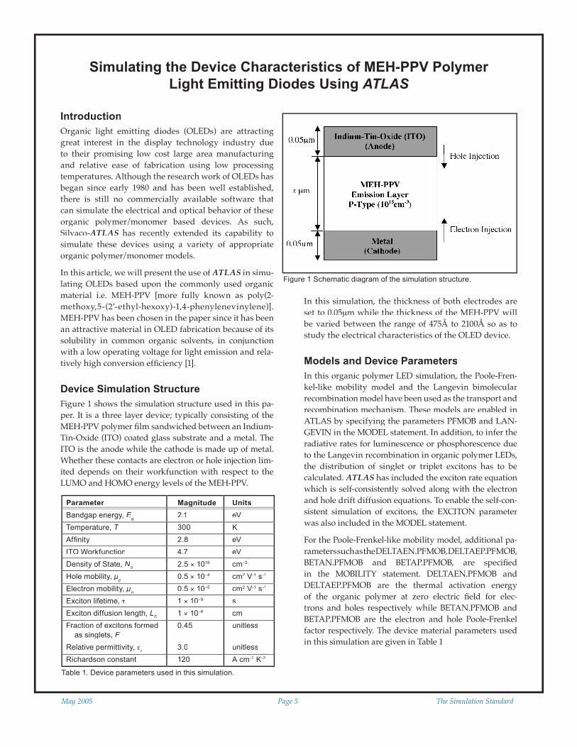
The “hole-only” device can be obtained by using a high workfunction metal such as In (4.2eV), Al(4.4.eV), Ag(4.6eV), Cu(4.7eV) or Au(5.2eV) at the cathode. The use of high workfunction metal contributes a high energy offset between the fermi energy at the cathode and the LUMO level in the MEH-PPV (which is 2.8eV). This ef-fectively reduces the number of injected electrons at the cathode and therefore the injected holes at the anode dominate. Figure 2 shows the current density versus
electric fi eld characteristics of a 1200Å thick OLED device with different metals. As can be seen from the graph, despite the fact that the workfunction of the cathode varies by more than 1eV between indium and gold, the simulated curves are identical, indicating that the electron injecting plays no part in determining the device characteristics.
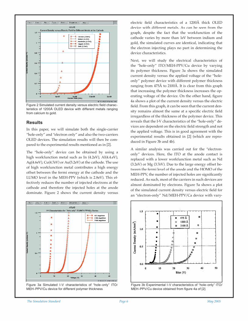
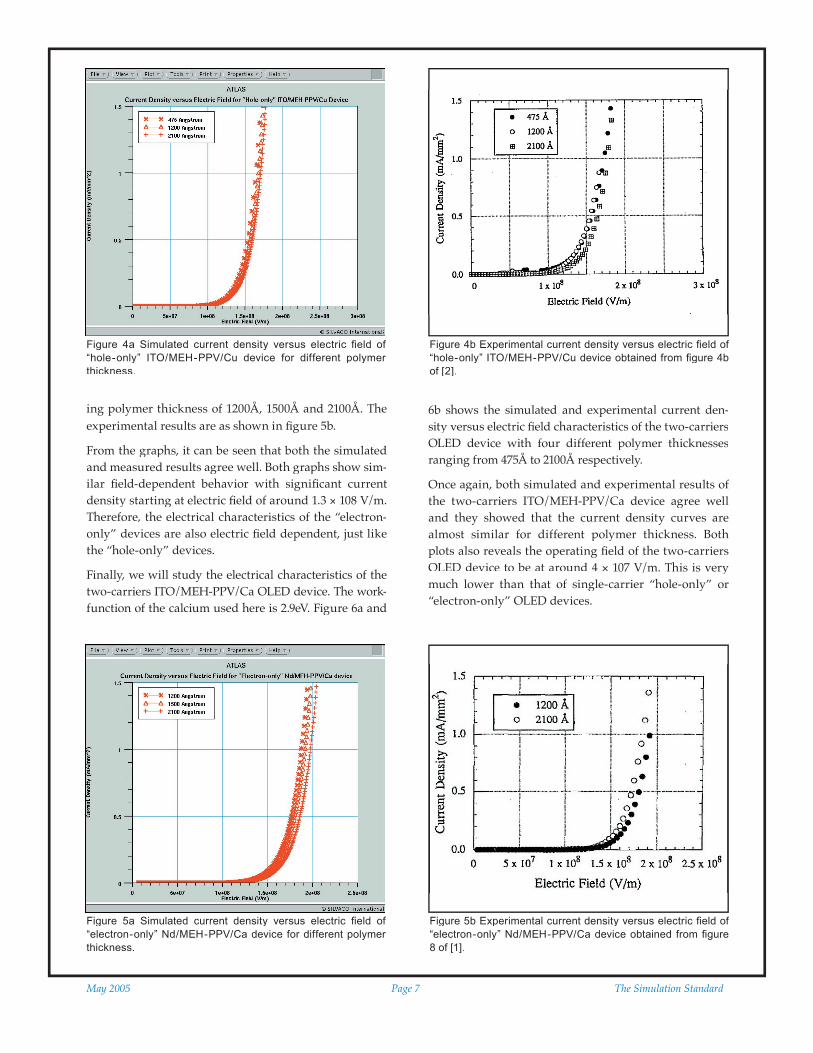
Next, we will study the electrical characteristics of the “hole-only” ITO/MEH-PPV/Cu device by varying its polymer thickness. Figure 3a shows the simulated current density versus the applied voltage of the “hole-only” polymer device with different polymer thickness ranging from 475Å to 2100Å. It is clear from this graph that increasing the polymer thickness increases the op-erating voltage of the device. On the other hand, fi gure 4a shows a plot of the current density versus the electric fi eld. From this graph, it can be seen that the current den-sity remains almost the same at a specifi c electric fi eld irregardless of the thickness of the polymer device. This reveals that the I-V characteristics of the “hole-only” de-vices are dependent on the electric fi eld strength and not the applied voltage. This is in good agreement with the experimental results obtained in [2] (which are repro-duced in Figure 3b and 4b).
A similar analysis was carried out for the “electron-only” devices. Here, the ITO at the anode contact is replaced with a lower workfunction metal such as Nd (3.2eV) or Mg (3.7eV). Due to the large energy offset be-tween the fermi level of the anode and the HOMO of the MEH-PPV, the number of injected holes are signifi cantly reduced. As such, most of the carriers in such devices are almost dominated by electrons. Figure 5a shows a plot of the simulated current density versus electric fi eld for an “electron-only” Nd/MEH-PPV/Ca device with vary-
Figure 2 Simulated current density versus electric fi eld charac-teristics of 1200Å OLED device with different metals ranging from calcium to gold.
Figure 3a Simulated I-V characteristics of “hole-only” ITO/MEH-PPV/Cu device for different polymer thickness.
Figure 3b Experimental I-V characteristics of “hole-only” ITO/MEH-PPV/Cu device obtained from fi gure 4a of [2].
The Simulation Standard Page 6 May 2005 May 2005 Page 7 The Simulation Standard
ing polymer thickness of 1200Å, 1500Å and 2100Å. The experimental results are as shown in fi gure 5b.
From the graphs, it can be seen that both the simulated and measured results agree well. Both graphs show sim-ilar fi eld-dependent behavior with signifi cant current density starting at electric fi eld of around 1.3 × 10⁸ V/m. Therefore, the electrical characteristics of the “electron-only” devices are also electric fi eld dependent, just like the “hole-only” devices.
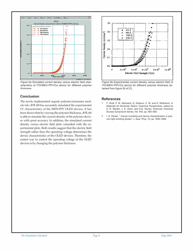
Finally, we will study the electrical characteristics of the two-carriers ITO/MEH-PPV/Ca OLED device. The work-function of the calcium used here is 2.9eV. Figure 6a and
6b shows the simulated and experimental current den-sity versus electric fi eld characteristics of the two-carriers OLED device with four different polymer thicknesses ranging from 475Å to 2100Å respectively.
Once again, both simulated and experimental results of the two-carriers ITO/MEH-PPV/Ca device agree well and they showed that the current density curves are almost similar for different polymer thickness. Both plots also reveals the operating fi eld of the two-carriers OLED device to be at around 4 × 10⁷ V/m. This is very much lower than that of single-carrier “hole-only” or “electron-only” OLED devices.
Figure 4a Simulated current density versus electric fi eld of “hole-only” ITO/MEH-PPV/Cu device for different polymer thickness.
Figure 4b Experimental current density versus electric fi eld of “hole-only” ITO/MEH-PPV/Cu device obtained from fi gure 4b of [2].
Figure 5a Simulated current density versus electric fi eld of “electron-only” Nd/MEH-PPV/Ca device for different polymer thickness.
Figure 5b Experimental current density versus electric fi eld of “electron-only” Nd/MEH-PPV/Ca device obtained from fi gure 8 of [1].
The Simulation Standard Page 8 May 2005 May 2005 Page 9 The Simulation Standard
ConclusionThe newly implemented organic polymer/monomer mod-ule into ATLAS has accurately simulated the experimental I-V characteristics of the MEH-PPV OLED devices. It has been shown that by varying the polymer thickness, ATLAS is able to simulate the current density of the polymer devic-es with great accuracy. In addition, the simulated current density versus electric fi eld plots coincided with the ex-perimental plots. Both results suggest that the electric fi eld strength rather than the operating voltage determines the device characteristics of the OLED devices. Therefore, the easiest way to control the operating voltage of the OLED devices is by changing the polymer thickness.
References1. F. Wudl, P. M. Allemand, G. Srdanov, Z. Ni, and D. McBranch, in
Materials for Nonlinear Optics: Chemical Perspectives, edited by S. R. Marder, J. E. Sohn, and G.D. Stucky, American Chemical Society Symposium Series, Vol. 455, pp. 683-686.
2. I. D. Parker, “ Carrier tunneling and device characteristics in poly-mer light-emitting diodes”, J. Appl. Phys. 75, pp. 1656-1666.
Figure 6a Simulated current density versus electric fi eld char-acteristics of ITO/MEH-PPV/Ca device for different polymer thickness.
Figure 6b Experimental current density versus electric fi eld of ITO/MEH-PPV/Ca device for different polymer thickness ob-tained from fi gure 2b of [1].