Simplified Block Diagram - Renesas Electronics
66
1 ©2021 Renesas Electronics Corporation April 8, 2021 Description The 8V97003 is a high-performance mmWave wideband Synthesizer / Phase Lock Loop (PLL) that generates output frequencies up to 18GHz from an integrated Voltage Controlled Oscillator (VCO) offering an octave of frequency tuning range. The device also offers a high-performance 32-bit fractional feedback divider and an output divider to allow users to fully benefit from the wideband characteristics of the VCO. The device's figure of merit (FOM) of -236dBc/Hz and the excellent VCO performance allow for very low phase noise and RMS phase jitter. The 8V97003 offers a very low output-to-output phase skew drift of < 10° across all operating conditions and frequencies, reducing radio path recalibration occurrences in beamforming applications, such as 5G radio card massive MIMO systems. The output drivers have programmable output power settings and can deliver high single-ended output power up of +12dBm at 8GHz, and +4dBm at 18GHz, when using inductively loaded output terminations (double termination). When the outputs are resistively loaded, the output drivers can deliver a single-ended output power of +9.5dBm at 8GHz, and up to -2.5dBm at 18GHz. The output power can be further increased when using differential outputs and measuring the output power differentially. The 8V97003 relies on a single 3.3V power supply and offers low noise integrated LDOs for excellent power supply noise immunity. Typical Applications ▪ 5G millimeter wave wireless infrastructure ▪ Massive MIMO ▪ Phase Array Antennas and beam forming ▪ Wireless backhaul ▪ Point-to-point and point-to-multipoint microwave links ▪ Satellites / VSATs ▪ Test equipment/instrumentation ▪ Clock generation ▪ High-speed RF converters sampling clocks ▪ Radar Features ▪ Output frequency range: 171.875MHz to 18GHz ▪ Ultra-low phase noise VCO • -60.6dBc integrated phase jitter (35fs rms jitter) from 20kHz to 100MHz at 6GHz ▪ Figure of Merit: -236dBc/Hz ▪ Input reference frequency: • 10MHz to 1.6GHz (LVPECL, LVDS) • 10MHz to 250MHz (LVCMOS) ▪ Fractional-N synthesizer and integer-N synthesizer ▪ 32-bit of fractional and modulus resolution ▪ Phase frequency detector (PFD) operation up to 500MHz (Integer mode) or 250MHz (Fractional mode) ▪ Programmable RF output power levels ▪ RF output power < -80dBm when in MUTE ▪ Programmable input multiplier (MULT) to increase PFD frequency when using a low input frequency ▪ -40°C to +95°C ambient temperature range; and up to +105°C board temperature ▪ 3.3V single power supply operation ▪ 7 7 mm 48-VFQFPN package ▪ SPI interface is compatible with 1.8V logic and tolerant to 3.3V ▪ Supported in the Timing Commander TM design tool Simplified Block Diagram x2 ÷R PLL x2 ÷M0 16-Bit Integer + 32-Bit Fractional Registers 2x RF Out 0.171-18GHz Clock Input SPI Loop Filter 171.875MHz to 18GHz RF / mmWave Wideband Synthesizer with Integrated VCO 8V97003 Datasheet
Transcript of Simplified Block Diagram - Renesas Electronics

1©2021 Renesas Electronics Corporation April 8, 2021
DescriptionThe 8V97003 is a high-performance mmWave wideband Synthesizer / Phase Lock Loop (PLL) that generates output frequencies up to 18GHz from an integrated Voltage Controlled Oscillator (VCO) offering an octave of frequency tuning range. The device also offers a high-performance 32-bit fractional feedback divider and an output divider to allow users to fully benefit from the wideband characteristics of the VCO.
The device's figure of merit (FOM) of -236dBc/Hz and the excellent VCO performance allow for very low phase noise and RMS phase jitter.
The 8V97003 offers a very low output-to-output phase skew drift of < 10° across all operating conditions and frequencies, reducing radio path recalibration occurrences in beamforming applications, such as 5G radio card massive MIMO systems.
The output drivers have programmable output power settings and can deliver high single-ended output power up of +12dBm at 8GHz, and +4dBm at 18GHz, when using inductively loaded output terminations (double termination). When the outputs are resistively loaded, the output drivers can deliver a single-ended output power of +9.5dBm at 8GHz, and up to -2.5dBm at 18GHz. The output power can be further increased when using differential outputs and measuring the output power differentially.
The 8V97003 relies on a single 3.3V power supply and offers low noise integrated LDOs for excellent power supply noise immunity.
Typical Applications 5G millimeter wave wireless infrastructure
Massive MIMO
Phase Array Antennas and beam forming
Wireless backhaul
Point-to-point and point-to-multipoint microwave links
Satellites / VSATs
Test equipment/instrumentation
Clock generation
High-speed RF converters sampling clocks
Radar
Features Output frequency range: 171.875MHz to 18GHz
Ultra-low phase noise VCO
• -60.6dBc integrated phase jitter (35fs rms jitter) from 20kHz to 100MHz at 6GHz
Figure of Merit: -236dBc/Hz
Input reference frequency:
• 10MHz to 1.6GHz (LVPECL, LVDS)
• 10MHz to 250MHz (LVCMOS)
Fractional-N synthesizer and integer-N synthesizer
32-bit of fractional and modulus resolution
Phase frequency detector (PFD) operation up to 500MHz (Integer mode) or 250MHz (Fractional mode)
Programmable RF output power levels
RF output power < -80dBm when in MUTE
Programmable input multiplier (MULT) to increase PFD frequency when using a low input frequency
-40°C to +95°C ambient temperature range; and up to +105°C board temperature
3.3V single power supply operation
7 7 mm 48-VFQFPN package
SPI interface is compatible with 1.8V logic and tolerant to 3.3V
Supported in the Timing CommanderTM design tool
Simplified Block Diagram
x2 ÷R PLL
x2
÷M016-Bit Integer +32-Bit Fractional
Registers
2x RF Out
0.171-18GHz
ClockInput
SPI
LoopFilter
171.875MHz to 18GHz RF / mmWave Wideband Synthesizer with Integrated VCO
8V97003Datasheet

2©2021 Renesas Electronics Corporation April 8, 2021
8V97003 Datasheet
Block Diagram
16-bit Int / 32-bit Frac
Divider
MUTE
LD
Logic and Registers
RF_OUTAnRF_OUTA
Lock Detect
CE
CPOUT
VTUNE
PFDCharge PumpREF_IN
RF_OUTBnRF_OUTB
SPI
SDOSDIOSCLKCSB
nRESET
8V97003
x2
÷RMULT
x2
/M0
ExternalLoop Filter
nREF_IN
SYNC

3©2021 Renesas Electronics Corporation April 8, 2021
8V97003 Datasheet
ContentsDescription ........................................................................................................................................................................................................... 1Typical Applications.............................................................................................................................................................................................. 1Features ............................................................................................................................................................................................................... 1Simplified Block Diagram ..................................................................................................................................................................................... 1Block Diagram ...................................................................................................................................................................................................... 2Contents ................................................................................................................................................................................................................ 3Pin Assignments................................................................................................................................................................................................... 8Pin Descriptions ................................................................................................................................................................................................... 8Absolute Maximum Ratings................................................................................................................................................................................ 11Recommended Operating Conditions ................................................................................................................................................................ 11Thermal Characteristics and Reliability Information ........................................................................................................................................... 12DC Electrical Characteristics ............................................................................................................................................................................. 12AC Electrical Characteristics .............................................................................................................................................................................. 15Typical Performance Characteristics.................................................................................................................................................................. 18Theory of Operation ........................................................................................................................................................................................... 21
Synthesizer Programming........................................................................................................................................................................... 22Reference Input Stage ................................................................................................................................................................................ 22Input Reference Divider (R) ........................................................................................................................................................................ 23Reference Doubler ...................................................................................................................................................................................... 23Reference Multiplier (MULT) ....................................................................................................................................................................... 23Feedback Divider ........................................................................................................................................................................................ 23Phase and Frequency Detector (PFD) and Charge Pump.......................................................................................................................... 25PFD Frequency ........................................................................................................................................................................................... 25External Loop Filter ..................................................................................................................................................................................... 25Charge Pump High-Impedance................................................................................................................................................................... 25Integrated Low Noise VCO ......................................................................................................................................................................... 26Output Clock Distribution and Optional Output Doubler.............................................................................................................................. 26Output Matching.......................................................................................................................................................................................... 27Band Selection Disable ............................................................................................................................................................................... 27Phase Adjust ............................................................................................................................................................................................... 28RF Output Power ........................................................................................................................................................................................ 28Output Phase Synchronization.................................................................................................................................................................... 28
Input-to-Output .................................................................................................................................................................................. 28Output Phases of Multiple 8V97003 Devices .................................................................................................................................... 28
Power-Down Mode...................................................................................................................................................................................... 29Default Power-Up Conditions...................................................................................................................................................................... 29VCO Calibration .......................................................................................................................................................................................... 29
3- or 4-Wire SPI Interface Description................................................................................................................................................................ 293/4-Wire Mode............................................................................................................................................................................................. 29Active Clock Edge....................................................................................................................................................................................... 29Reset........................................................................................................................................................................................................... 29Least Significant Bit Position....................................................................................................................................................................... 30Addressing .................................................................................................................................................................................................. 30Read Operation........................................................................................................................................................................................... 30Mirrored Register Bits ................................................................................................................................................................................. 30Double-Buffered Registers.......................................................................................................................................................................... 30Operation Protocols .................................................................................................................................................................................... 31

4©2021 Renesas Electronics Corporation April 8, 2021
8V97003 Datasheet
Register Map ...................................................................................................................................................................................................... 35Register Block Descriptions ........................................................................................................................................................................ 38Preface Registers........................................................................................................................................................................................ 39Feedback Divider Control Registers ........................................................................................................................................................... 41Phase Adjustments Control Registers ........................................................................................................................................................ 43DSM Control Registers ............................................................................................................................................................................... 44Calibration Control Registers ...................................................................................................................................................................... 45Band Select Clock Divider Control Registers.............................................................................................................................................. 46Lock Detect Control Registers .................................................................................................................................................................... 47Power Down Control Registers ................................................................................................................................................................... 48Input Control Registers ............................................................................................................................................................................... 49Charge Pump Control Registers ................................................................................................................................................................. 51Re-Sync Control Registers.......................................................................................................................................................................... 52Output Control Registers............................................................................................................................................................................. 53Status Registers.......................................................................................................................................................................................... 55
Applications Information ..................................................................................................................................................................................... 56Loop Filter Calculations............................................................................................................................................................................... 56
2nd Order Loop Filter ........................................................................................................................................................................ 563rd Order Loop Filter ......................................................................................................................................................................... 58
Recommendations for Unused Input and Output Pins................................................................................................................................ 59Inputs................................................................................................................................................................................................. 59Outputs.............................................................................................................................................................................................. 59
Schematic Example .................................................................................................................................................................................... 59Power Considerations ........................................................................................................................................................................................ 60Package Outline Drawings ................................................................................................................................................................................. 61Marking Diagram ............................................................................................................................................................................................... 61Ordering Information .......................................................................................................................................................................................... 62Revision History ................................................................................................................................................................................................. 63

5©2021 Renesas Electronics Corporation April 8, 2021
8V97003 Datasheet
List of FiguresFigure 1. Pin Assignments for 7 × 7 mm 48-VFQFPN Package ― Top View ................................................................................................... 8Figure 2. Phase Noise at 6GHz (Fractional Mode).......................................................................................................................................... 18Figure 3. Phase Noise at 6GHz (Integer Mode) .............................................................................................................................................. 18Figure 4. Phase Noise at 8GHz (Integer Mode) .............................................................................................................................................. 19Figure 5. Phase Noise at 11GHz (Integer Mode) ............................................................................................................................................ 19Figure 6. Phase Noise at 18GHz (Integer Mode) ............................................................................................................................................ 20Figure 7. Phase Noise at 8GHz (Open Loop).................................................................................................................................................. 20Figure 8. Typical Output Power vs. RF Output Frequency (Over Different Loads).......................................................................................... 21Figure 9. Test Setup for RF Output Power Measurement ............................................................................................................................... 21Figure 10. Input Reference Path........................................................................................................................................................................ 22Figure 11. RF Feedback N Divider .................................................................................................................................................................... 23Figure 12. Simplified PFD Circuit using D-type Flip-Flop................................................................................................................................... 25Figure 13. Output Clock Distribution ................................................................................................................................................................. 26Figure 14. Output Stage .................................................................................................................................................................................... 26Figure 15. Resistive Matching Termination ...................................................................................................................................................... 27Figure 16. Inductively Loaded Termination ....................................................................................................................................................... 27Figure 17. 4-Wire MSB First, Single Byte Write and Read ................................................................................................................................ 31Figure 18. 4-Wire LSB First, Single Byte Write and Read ................................................................................................................................. 32Figure 19. 4-Wire MSB First, Multiple Bytes Write (2 Bytes Shown as Example) ............................................................................................. 32Figure 20. 4-Wire LSB First, Multiple Bytes Read (2 Bytes Shown as Example) .............................................................................................. 33Figure 21. 3-Wire MSB First, Single Byte Read and Write ................................................................................................................................ 33Figure 22. SPI Timing Diagram ......................................................................................................................................................................... 34Figure 23. Typical 2nd Order Loop Filter ............................................................................................................................................................ 56Figure 24. Typical 3rd Order Loop Filter ........................................................................................................................................................... 58Figure 25. Loop Filter Example.......................................................................................................................................................................... 58Figure 26. Schematic Example.......................................................................................................................................................................... 60

6©2021 Renesas Electronics Corporation April 8, 2021
8V97003 Datasheet
List of TablesTable 1. Pin Descriptions .................................................................................................................................................................................. 8Table 2. Pin Characteristics ............................................................................................................................................................................ 10Table 3. Supply Pins and Associated Current Return Paths........................................................................................................................... 10Table 4. Absolute Maximum Ratings .............................................................................................................................................................. 11Table 5. Recommended Operating Conditions............................................................................................................................................... 11Table 6. Thermal Characteristics .................................................................................................................................................................... 12Table 7. Thermal Resistance θJA for 48-VFQFPN, Forced Convection......................................................................................................... 12Table 8. Power Supply DC Characteristics, VDDx = 3.3V ±5%, TA = -40°C to +95°C (Not Exceeding Max. Board or Junction Temp.) ...... 12Table 9. Typical Current by Power Domain .................................................................................................................................................... 13Table 10. LVCMOS DC Characteristics, VDDx = 3.3V ±5%, TA = -40°C to +95°C (Not Exceeding Max. Board or Junction Temp.) ............. 14Table 11. AC Characteristics, VDDx = 3.3V ±5%, TA = -40°C to +95°C (Not Exceeding Maximum Board or Junction Temp.)...................... 15Table 12. RF_OUT[A:B] Phase Noise Char., VDDx = 3.3V ±5%, TA = -40°C to +95°C (Not Exceeding Max. Board or Junction Temp.) ...... 16Table 13. Fractional Spurs Due to the Quantization Noise............................................................................................................................... 24Table 14. Timing Requirements ........................................................................................................................................................................ 28Table 15. SPI Read / Write Cycle Timing Parameters ...................................................................................................................................... 34Table 16. Preface Registers ............................................................................................................................................................................. 35Table 17. Control Registers .............................................................................................................................................................................. 35Table 18. Status Registers................................................................................................................................................................................ 37Table 19. Register Block Descriptions .............................................................................................................................................................. 38Table 20. Preface Register Block ..................................................................................................................................................................... 39Table 21. Preface Register Bits ........................................................................................................................................................................ 39Table 22. Preface Register Description ............................................................................................................................................................ 40Table 23. Feedback Divider Control Block........................................................................................................................................................ 41Table 24. Feedback Divider Control Register Bits ............................................................................................................................................ 41Table 25. Feedback Divider Control Register Description ................................................................................................................................ 42Table 26. Phase Adjustments Control Register Block ...................................................................................................................................... 43Table 27. Phase Adjustments Control Register Bits ......................................................................................................................................... 43Table 28. Phase Adjustments Control Register Descriptions ........................................................................................................................... 43Table 29. DSM Control Register Block ............................................................................................................................................................. 44Table 30. DSM Control Register Bits ................................................................................................................................................................ 44Table 31. DSM Control Register Descriptions .................................................................................................................................................. 44Table 32. Calibration Control Register Block .................................................................................................................................................... 45Table 33. Calibration Control Register Bits ....................................................................................................................................................... 45Table 34. Calibration Control Register Descriptions ......................................................................................................................................... 45Table 35. Band Select Clock Divider Control Register Block............................................................................................................................ 46Table 36. Band Select Clock Divider Control Register Bits............................................................................................................................... 46Table 37. Band Select Clock Divider Control Register Descriptions................................................................................................................. 46Table 38. Lock Detect Control Register Block .................................................................................................................................................. 47Table 39. Lock Detect Control Register Bits ..................................................................................................................................................... 47Table 40. Lock Detect Control Register Descriptions ....................................................................................................................................... 47Table 41. Power Down Control Register Block................................................................................................................................................. 48Table 42. Power Down Control Register Bits.................................................................................................................................................... 48Table 43. Power Down Control Register Descriptions ...................................................................................................................................... 48Table 44. Input Control Register Block ............................................................................................................................................................. 49Table 45. Input Control Register Bits ................................................................................................................................................................ 49Table 46. Input Control Register Descriptions .................................................................................................................................................. 49Table 47. Charge Pump Control Register Block ............................................................................................................................................... 51Table 48. Charge Pump Control Register Bits .................................................................................................................................................. 51

7©2021 Renesas Electronics Corporation April 8, 2021
8V97003 Datasheet
Table 49. Charge Pump Control Register Descriptions .................................................................................................................................... 51Table 50. Re-Sync Control Register Block........................................................................................................................................................ 52Table 51. Re-sync Control Register Bits ........................................................................................................................................................... 52Table 52. Re-sync Control Register Descriptions ............................................................................................................................................. 52Table 53. Output Control Register Block........................................................................................................................................................... 53Table 54. Output Control Register Bits ............................................................................................................................................................. 53Table 55. Output Control Register Descriptions................................................................................................................................................ 53Table 56. Status Register Block........................................................................................................................................................................ 55Table 57. Status Register Bits .......................................................................................................................................................................... 55Table 58. Status Register Descriptions............................................................................................................................................................. 55Table 59. Ordering Information ......................................................................................................................................................................... 62Table 60. Pin 1 Orientation in Tape and Reel Packaging ................................................................................................................................. 62

8©2021 Renesas Electronics Corporation April 8, 2021
8V97003 Datasheet
Pin AssignmentsFigure 1. Pin Assignments for 7 × 7 mm 48-VFQFPN Package ― Top View
Pin DescriptionsTable 1. Pin Descriptions
Pin Number Name TypePull-up/
Pull-Down Description
1 VREFVCO2 Analog Reference node for VCO regulator. Connect 22µF capacitor from this pin to GND.
2 NC Unused Do not connect.
3 VDDVCO2 Power VDD power supply for VCO.
4 VREGVCO2 Analog Regulator for VCO. Connect 22µF capacitor from this pin to GND.
5 VTUNE Analog VCO Tuning Voltage.
6 NC Unused Do not connect.
7 MUTE Input PD Outputs disable / High-Impedance. 1.8V LVCMOS logic levels (3.3V tolerant).
8 LD Output Lock Detector (CMOS).
9 NC Unused Do not connect.
10 CPOUT Analog Charge Pump Output.
NC
VREFVCO2 36
35
34
33
32
31
30
28
29
27
26
2513 14 15 16 17 18 19 20 21 22 23 24
1
2
3
4
5
6
7
9
8
10
11
12
48 47 46 45 44 43 42 41 40 39 38 37
VREGVCO2
VDDVCO2
NC
VTUNE
LD
MUTE
CPOUT
NC
VDDPDCP
CPBIAS
NC
VREFVCO1
VDDVCO1
NC
nRESET
VREGVCO1
CE
SYNC
SDO
SDIO
CSB
SCLK
8V97003

9©2021 Renesas Electronics Corporation April 8, 2021
8V97003 Datasheet
11 CPBIAS Analog Bias node for charge pump. Connect 22µF capacitor from this pin to GND.
12 VDDPDCP Power VDD power supply for phase detector and charge pump.
13 NC Unused Do not connect.
14 VSSPDCP Ground VSS power supply ground for phase detector and charge pump.
15 VDDFB Power VDD power supply for feedback divider.
16 NC Unused Do not connect.
17 VSSFB Ground VSS power supply ground for feedback divider.
18 VDDDIG Power VDD power supply for Digital, SPI and SDM.
19 VSSDIG Ground VSS power supply ground for Digital, SPI and SDM.
20 VSSIN Ground VSS power supply ground for reference input path.
21 NC Unused Do not connect.
22 REF_IN Input PD Differential reference clock input+ (LVDS, LVPECL, CMOS).
23 nREF_IN Input PD/PU Differential reference clock input– (LVDS, LVPECL).
24 VDDIN Power VDD power supply for reference input path.
25 CSB Input PD SPI Chip Select Bar. 1.8V LVCMOS logic levels (3.3V tolerant).
26 SCLK Input SPI Clock Input. 1.8V LVCMOS logic levels (3.3V tolerant).
27 SDO Output SPI Data Output.
28 SDIO Input/Output PU SPI Data Input/ Output. 1.8V LVCMOS logic levels (3.3V tolerant).
29 CE Input PU Chip Enable. 1.8V LVCMOS logic levels (3.3V tolerant).
CE = 0: Power-down mode
CE = 1: Normal operation
30 SYNC Input PD
SYNC pin can be used to implement a deterministic delay between the reference input rising edge and the output signal rising edge.
If not used, this pin can either be tied to ground, or left floating since it has an internal pulldown. 3.3V LVCMOS input.
31 nRESET Input PU Chip Reset. 1.8V LVCMOS logic levels (3.3V tolerant).
32 VREGVCO1 Analog Regulator for VCO. Connect 22µF capacitor from this pin to GND.
33 VDDVCO1 Power VDD power supply for VCO.
34 NC Unused Do not connect.
35 VREFVCO1 AnalogReference node for VCO regulator. Connect 22µF capacitor from this pin to GND.
36 NC Unused Do not connect.
37 VDDOUTA Power VDD output power supply for output pair A.
38 VSSOUTA Ground VSS power supply ground for output pair A.
39 nRF_OUTA OutputNegative side of output pair A (CML – Open Collector). The output power level is programmable.
Table 1. Pin Descriptions (Cont.)
Pin Number Name TypePull-up/
Pull-Down Description

10©2021 Renesas Electronics Corporation April 8, 2021
8V97003 Datasheet
40 RF_OUTA OutputPositive side of output pair A (CML – Open Collector). The output power level is programmable.
41 VSSOUTA Ground VSS power supply ground for output pair A.
42 NC Analog Do not connect.
43 NC Analog Do not connect.
44 VSSOUTB Ground VSS power supply ground for output pair B.
45 RF_OUTB Output Positive side of output pair B (CML – open collector). The output power level is programmable.
46 nRF_OUTB OutputNegative side of output pair B (CML – open collector). The output power level is programmable.
47 VSSOUTB Ground VSS power supply ground for output pair B.
48 VDDOUTB Power VDD output power supply output pair B.
EP EPAD Ground Must be connected to ground.
Table 2. Pin Characteristics
Symbol Parameter Test Condition Minimum Typical Maximum Units
CIN Input Capacitance REF_IN, nREF_IN 1 pF
ROUT LVCMOS Output Impedance LD 15 Ω
RPULLUP Input Pullup Resistor 50 kΩ
RPULLDOWN Input Pulldown Resistor 50 kΩ
Table 3. Supply Pins and Associated Current Return Paths
Power Supply Associated Ground
Pin Number Pin Name Pin Number Pin Name
3 VDDVCO2 EP EPAD
12 VDDPDCP 14 VSSPDCP
15 VDDFB 17 VSSFB
18 VDDDIG 19 VSSDIG
24 VDDIN 20 VSSIN
33 VDDVCO1 EP EPAD
37 VDDOUTA 38; 41 VSSOUTA
48 VDDOUTB 44; 47 VSSOUTB
Table 1. Pin Descriptions (Cont.)
Pin Number Name TypePull-up/
Pull-Down Description

11©2021 Renesas Electronics Corporation April 8, 2021
8V97003 Datasheet
Absolute Maximum RatingsThe absolute maximum ratings are stress ratings only. Stresses greater than those listed below can cause permanent damage to the device. Functional operation of the 8V97003 at absolute maximum ratings is not implied. Exposure to absolute maximum rating conditions may affect device reliability.
Recommended Operating Conditions
Table 4. Absolute Maximum Ratings[a]
[a] Over operating ambient temperature range (unless otherwise indicated).
Symbol Parameter Rating Units
VDDx[b]
[b] VDDx denotes, VDDVCO2, VDDPDCP, VDDFB, VDDDIG, VDDIN, VDDVCO1, VDDOUTA, VDDOUTB.
Supply Voltage 3.63 V
VIInput Voltage (REF_IN, nREF_IN, MUTE, SDIO, VTUNE, SCLK, CSB, CE, nRESET, and SYNC)
-0.5 to VDDx[a] +0.5 V
VoOutput Voltage (RF_OUTA, nRF_OUTA, RF_OUTB, nRF_OUTB, LD, CPOUT, SDIO, SDO)
-0.5 to VDDx[a] +0.5 V
I0 Output CurrentContinuous Current 60 mA
Surge Current 90 mA
I0 Output Current (SDO, SDIO, LD)Continuous Current 40 mA
Surge Current 65 mA
TJ Maximum Junction Temperature 150 °C
TS Storage Temperature -65 to 150 °C
— ESD – Human Body Model 2000 V
— ESD – Charged Device Model 750 V
Table 5. Recommended Operating Conditions[a][b]
[a] It is the user’s responsibility to ensure that device junction temperature remains below the maximum allowed.
[b] All conditions in this table must be met to guarantee device functionality.
Symbol Parameter Minimum Typical Maximum Units
TA Ambient Air Temperature -40 +95 °C
TB Board Temperature[c]
[c] Measured at solder connection to printed circuit board on exposed pad.
+105 °C
TJ Junction Temperature +125 °C

12©2021 Renesas Electronics Corporation April 8, 2021
8V97003 Datasheet
Thermal Characteristics and Reliability Information
DC Electrical Characteristics
Table 6. Thermal Characteristics
Symbol Parameter Value Units
θJB Theta JB. Junction to board 0.76 °C/W
θJC Theta JC. Junction to case 10.33 °C/W
Table 7. Thermal Resistance θJA for 48-VFQFPN, Forced Convection
θJA by Velocity
Air Flow 0 1 2 m/s
Multi-Layer PCB, JEDEC Standard Test Boards 22.3 18.84 17.3 °C/W
Table 8. Power Supply DC Characteristics, VDDx = 3.3V ±5%, TA = -40°C to +95°C (Not Exceeding Max. Board or Junction Temp.)[a][b][c]
[a] RF outputs terminated to 50Ω to VDDOUT[A:B].
[b] Output power set to 0101 (see RF_OUTx_pwr[3:0] in Table 55).
[c] Over Recommended Operating Conditions (unless otherwise indicated).
Symbol Parameter Conditions Minimum Typical Maximum Units
VDDx[d]
[d] VDDx denotes, VDDVCO2, VDDPDCP, VDDFB, VDDDIG, VDDIN, VDDVCO1, VDDOUTA, VDDOUTB.
Power Supply Voltage 3.135 3.3 3.465 V
IDDx[e]
[e] IDDx denotes IDDVCO2, IDDPDCP, IDDFB, IDDDIG, IDDIN, IDDVCO1, IDDOUTA, IDDOUTB.
Power Supply Current[f]
[f] Input Frequency = 122.88MHz, Input Doubler Enabled, Output Frequency = 6GHz; PLL is in Fractional mode.
RF_OUTA, nRF_OUTA – Active
RF_OUTB, nRF_OUTB – Muted516 590 mA
RF_OUTA, nRF_OUTA – Active
RF_OUTB, nRF_OUTB – Active566 650 mA
RF_OUTA, nRF_OUTA – Muted
RF_OUTB, nRF_OUTB – Muted464 538 mA
IVCO VCO Supply Current VCO Frequency = 6GHz 225 271 mA
— Power Down Current[g]
[g] VCO_EN is located in register 0x28, bit position 0. CE: Chip Enable, pin 29.
VCO Frequency = 6GHz, CE = Low, VCO_EN = 1
250 302 mA
CE = Low, VCO_EN = 0[h]
[h] Power Down Current with VCO_EN = 0 and CE = Low is independent of the VCO frequency.
71 90 mA

13©2021 Renesas Electronics Corporation April 8, 2021
8V97003 Datasheet
Table 9. Typical Current by Power Domain[a][b]
Pin Name Pin Number Condition Typical Unit
VDDVCO2, VDDVCO1[c] 3, 33
8GHz VCO frequency270 mA
VDDPDCP 12 ICP = 8mA 65 mA
VDDFB 15 49 mA
VDDDIG 18
PFD frequency: 245.76MHz
DSM setting: 3rd Order (Fractional mode)34 mA
PFD frequency: 245.76MHz
DSM OFF (Integer Mode)23 mA
VDDIN 24 Input doubler OFF, MULT OFF, Input divider OFF 36 mA
VDDOUTA 37
RF_OUT Disabled 10 mA
RF_OUTA Enabled; RF Output Power Setting: 0001 (Minimum setting) 43 mA
RF_OUTA Enabled; RF Output Power Setting: 1100 (Maximum setting) 82 mA
VDDOUTB 48
RF_OUTB Disabled 54 mA
RF_OUTB Enabled; RF Output Power Setting: 0001 (Minimum setting) 88 mA
RF_OUTB Enabled; RF Output Power Setting: 1100 (Maximum setting) 126 mA
RF_OUTB Enabled; RF Output Power Setting: 1100; Output doubler ON 137 mA
RF_OUTB Enabled; RF Output Power Setting: 0010; Output Divider: Divide by 2
89 mA
[a] Operating conditions are: REF_IN = 122.88MHz; RF_OUTA = RF_OUTB = 8GHz.
[b] Over Recommended Operating Conditions (unless otherwise indicated).
[c] Total current from VDDVCO1 and VDDVCO2 (externally connected).

14©2021 Renesas Electronics Corporation April 8, 2021
8V97003 Datasheet
Table 10. LVCMOS DC Characteristics, VDDx[a] = 3.3V ±5%, TA = -40°C to +95°C (Not Exceeding Max. Board or Junction Temp.)[b]
Symbol Parameter Test Conditions Minimum Typical Maximum Units
VIH Input High Voltage
nRESET, CE, MUTE, CSB, SCLK, SDIO
1.2 VDDx[a] V
SYNC 2 VDDx[a] V
VIL Input Low Voltage
nRESET, CE, MUTE, CSB, SCLK, SDIO
0.65 V
SYNC 0.8
IIH Input High CurrentnRESET, CE, SDIO VDDx = VIN = 3.465V 5 µA
CSB, MUTE, SYNC VDDx = VIN = 3.465V 150 µA
IIL Input Low CurrentnRESET, CE, SDIO VDDx = 3.465V, VIN = 0V -150 µA
CSB, MUTE, SYNC VDDx = 3.465V, VIN = 0V -5 µA
VOH Output High Voltage SDO, SDIO[c], LD VDDx = 3.465V, IOH = -2mA 2.4 V
VOL Output Low Voltage SDO, SDIO[c], LD VDDx = 3.465V, IOL = 2mA 0.4 V
[a] VDDx denotes, VDDVCO2, VDDPDCP, VDDFB, VDDDIG, VDDIN, VDDVCO1, VDDOUTA, VDDOUTB.
[b] Over Recommended Operating Conditions (unless otherwise indicated).
[c] SDIO as output.

15©2021 Renesas Electronics Corporation April 8, 2021
8V97003 Datasheet
AC Electrical CharacteristicsTable 11. AC Characteristics, VDDx[a] = 3.3V ±5%, TA = -40°C to +95°C (Not Exceeding Maximum Board or Junction Temp.)[b]
Symbol Parameter Test Conditions Minimum Typical Maximum Units
REF_IN Input Reference FrequencyReference doubler disabled 10 1600 MHz
Reference doubler enabled 10 250 MHz
VPP REF_IN Input Sensitivity Biased at VDDx/2[c] 0.4 VDDx[a] V
fVCO VCO Frequency Fundamental VCO mode 5,500 11,000 MHz
fRF_OUT Output FrequencyOutput doubler disabled 171.875 11,000 MHz
Output doubler enabled 11,000 18,000 MHz
fPFD PFD FrequencyFractional mode 250 MHz
Integer mode 500 MHz
KVCO VCO Sensitivity[d]
VCO Frequency = 5.625GHz 100
MHz/V
VCO Frequency = 6.23GHz 120
VCO Frequency = 6.975GHz 140
VCO Frequency = 7.8GHz 160
VCO Frequency = 8.65GHz 210
VCO Frequency = 9.575GHz 165
VCO Frequency = 10.3GHz 155
VCO Frequency = 10.9GHz 170
tLOCK
PLL Lock Time[e] Time from Low to High of CSB until Low to High of LD
1 ms
Frequency Lock TimeOne frequency to another frequency locking time when VCO calibration is bypassed.
70 µs
-Single-Ended RF Output Power[f]
Muted < -80 dBm
RF_OUTn_pwr = 1100 (max)
50-ohm Resistive Loading
RF_OUT = 8GHz 9.5 dBm
RF_OUT = 18GHz -2.5 dBm
RF_OUTn_pwr = 0110
50-ohm Resistive Loading
RF_OUT = 8GHz 5 dBm
RF_OUT = 18GHz -6.5 dBm
RF_OUTn_pwr = 1100 (max)
1nH Inductive LoadingRF_OUT = 8GHz 12 dBm
RF_OUTn_pwr = 1100 (max)
0.6nH Inductive LoadingRF_OUT = 18GHz 4 dBm
-RF Output Power Variation Across Temperature[g]
RF_OUT at 11GHz ±2 dBm
RF_OUT from 11GHz to 18GHz
±4 dBm
-Min/Max VCO Tuning Voltage
0.3/2.2 V

16©2021 Renesas Electronics Corporation April 8, 2021
8V97003 Datasheet
- Output-to-Output Skew 5 ps
- Output-to-Output Skew DriftAny value of fRF_OUT. Measurement taken from -40°C to +95°C.
2 10 °
- Input-to-Output Skew DriftAny value of fRF_OUT. Measurement taken from -40°C to +95°C.
9 ps
[a] VDDx denotes VDDVCO2, VDDPDCP, VDDFB, VDDDIG, VDDIN, VDDVCO1, VDDOUTA, VDDOUTB.
[b] Over Recommended Operating Conditions (unless otherwise indicated).
[c] AC-coupling the reference signal ensures VDDx / 2 biasing.
[d] The value depends on VCO frequency.
[e] Band Select/Calibration Resolution = 4x (BandSelAcc[1:0]=10), fPFD/BndSelDiv ~100kHz.
[f] Single-Ended RF Output Power values are based on after de-embedding the trace and cable losses while other output is connected with same length of cable and terminated to 50ohm resistor. For test setup, see Figure 9. For output terminations, see Figure 26.
[g] Output Power setting = 0110b.
Table 12. RF_OUT[A:B] Phase Noise Char., VDDx[a] = 3.3V ±5%, TA = -40°C to +95°C (Not Exceeding Max. Board or Junction Temp.)[b]
Symbol Parameter Test Conditions Minimum Typical Maximum Units
tjit(Ø)Integrated Phase Noise/Jitter
fRF_OUT = 6GHz
Integration Range: 20kHz – 100MHz PFD = 245.76MHz (Fractional Mode)
-55 -48.8 dBc
66 fs RMS
fRF_OUT = 6GHz
Integration Range: 20kHz – 100MHz PFD = 500MHz (Integer Mode)
-60.6 -57.4 dBc
35 50 fs RMS
fRF_OUT = 8GHz
Integration Range: 20kHz – 100MHz PFD = 500MHz (Integer Mode)
-57.6 -55 dBc
36.8 50 fs RMS
fRF_OUT = 11GHz
Integration Range: 20 kHz – 100MHz PFD = 500MHz (Integer Mode)
-53.3 -47 dBc
44 82 fs RMS
fRF_OUT = 18GHz
Integration Range: 20 kHz – 100MHz
PFD = 250kHz (Integer Mode)
-50.2 -46.4 dBc
38.5 58 fs RMS
ΦN(10k)
RF Output Phase Noise Performance at 6GHz (Open Loop)
10kHz offset from carrier -74.9 -72.8 dBc/Hz
ΦN(100k) 100kHz offset from carrier -104.8 -102.7 dBc/Hz
ΦN(1M) 1MHz offset from carrier -133.2 -130.9 dBc/Hz
ΦN(10M) 10MHz offset from carrier -153.8 -152.6 dBc/Hz
ΦN(60M) 60MHz offset from carrier -157.8 -156.8 dBc/Hz
Table 11. AC Characteristics, VDDx[a] = 3.3V ±5%, TA = -40°C to +95°C (Not Exceeding Maximum Board or Junction Temp.)[b] (Cont.)
Symbol Parameter Test Conditions Minimum Typical Maximum Units

17©2021 Renesas Electronics Corporation April 8, 2021
8V97003 Datasheet
ΦN(10k)
RF Output Phase Noise Performance at 8GHz (Open Loop)
10kHz offset from carrier -71.5 -69.3 dBc/Hz
ΦN(100k) 100kHz offset from carrier -101.9 -100.6 dBc/Hz
ΦN(1M) 1MHz offset from carrier -130.6 -128.4 dBc/Hz
ΦN(10M) 10MHz offset from carrier -152.1 -149.5 dBc/Hz
ΦN(60M) 60MHz offset from carrier -157.7 -155.7 dBc/Hz
ΦN(10k)
RF Output Phase Noise Performance at 11GHz (Open Loop)
10kHz offset from carrier -67.1 -65.2 dBc/Hz
ΦN(100k) 100kHz offset from carrier -98 -93.3 dBc/Hz
ΦN(1M) 1MHz offset from carrier -125.1 -114.2 dBc/Hz
ΦN(10M) 10MHz offset from carrier -144.7 -133.2 dBc/Hz
ΦN(60M) 60MHz offset from carrier -150.8 -142.2 dBc/Hz
ΦN(10k)
RF Output Phase Noise Performance at 18GHz (Open Loop)
10kHz offset from carrier -64.6 -62.7 dBc/Hz
ΦN(100k) 100kHz offset from carrier -95.5 -93.2 dBc/Hz
ΦN(1M) 1MHz offset from carrier -123.4 -119.9 dBc/Hz
ΦN(10M) 10MHz offset from carrier -144.1 -140.0 dBc/Hz
ΦN(60M) 60MHz offset from carrier -148.6 -142.1 dBc/Hz
—Spurious Signals due to PFD Frequency
fPFD = 245.76MHz; RF_OUT = 7.86432GHz; Integer Mode
-83.2 -77.5 dB
fPFD = 245.76MHz; RF_OUT = 8GHz; Fractional Mode
-74.1 -69.9 dB
ΦN(SYNTH)Normalized Phase Noise Floor
-236 dBc/Hz
ΦN(1/f) Normalized 1/f Noise[c] 10kHz Offset; fRF_OUT = 8GHz -132 dBc/Hz
H2 VCO second harmonic fVCO = 8GHz -36dB
H3 VCO third harmonic fVCO = 8GHz -33
[a] VDDx denotes VDDVCO2, VDDPDCP, VDDFB, VDDDIG, VDDIN, VDDVCO1, VDDOUTA, VDDOUTB.
[b] Over recommended operating conditions (unless otherwise indicated).
[c] N(1/f) = ΦN(RF_OUT) – 10 Log(10kHz ÷ f) – 20 Log (fRF_OUT ÷ 1GHz) where ΦN(1/f) is the 1/f noise contribution at a RF_OUT frequency (fRF_OUT) and at a frequency offset f.
Table 12. RF_OUT[A:B] Phase Noise Char., VDDx[a] = 3.3V ±5%, TA = -40°C to +95°C (Not Exceeding Max. Board or Junction Temp.)[b] (Cont.)
Symbol Parameter Test Conditions Minimum Typical Maximum Units

18©2021 Renesas Electronics Corporation April 8, 2021
8V97003 Datasheet
Typical Performance CharacteristicsFigure 2. Phase Noise at 6GHz (Fractional Mode)
Figure 3. Phase Noise at 6GHz (Integer Mode)

19©2021 Renesas Electronics Corporation April 8, 2021
8V97003 Datasheet
Figure 4. Phase Noise at 8GHz (Integer Mode)
Figure 5. Phase Noise at 11GHz (Integer Mode)

20©2021 Renesas Electronics Corporation April 8, 2021
8V97003 Datasheet
Figure 6. Phase Noise at 18GHz (Integer Mode)
Figure 7. Phase Noise at 8GHz (Open Loop)

21©2021 Renesas Electronics Corporation April 8, 2021
8V97003 Datasheet
Figure 8. Typical Output Power vs. RF Output Frequency (Over Different Loads)
Figure 9. Test Setup for RF Output Power Measurement
Theory of OperationThe 8V97003 is a high-performance frequency synthesizer with an integrated wideband VCO for wide frequency coverage. The VCO provides an octave frequency from 5.5GHz to 11GHz. An optional VCO-doubler is used to generate frequencies larger than the maximum VCO frequency (11GHz) up to 18GHz and an optional output divider can be used to divide the VCO frequency to an output frequency as low as 171.875 MHz. The input reference can support frequencies from 10MHz to 1600MHz. The phase detector (PFD) can support frequencies from 10MHz to 250MHz in fractional mode, and up to 500MHz in Integer mode. A Delta Sigma Modulator (DSM) controls the feedback divider of the PLL in order to create fractional N-divider values. The fractional numerator and the modulus are programmable to 32-bit long, allowing a very fine frequency resolution. The device provides two outputs with individually programmable RF output power (for more information, see Table 55). The digital logic is a 3- or 4-wire SPI interface that is 1.8V compatible and 3.3V tolerant.
‐6
‐4
‐2
0
2
4
6
8
10
12
14
16
4 5 6 7 8 9 10 11 12 13 14 15 16 17 18
RF O
utpu
t Pow
er, d
Bm
RF Output Frequency, GHz
RF_OUTn_pwr Setting = 1100 (Maximum)Single-Ended Output Power, dBm vs Output Frequency, GHz
Load_50ohm Load_1nH Load_0.6nH
8V97003
Vdd
Vdd
Spectrum Analyzer
50Ω
50Ω
50Ω
50Ω
22©2021 Renesas Electronics Corporation April 8, 2021
8V97003 Datasheet
Synthesizer ProgrammingThe Fractional-N divider architecture is implemented via a cascaded programmable dual modulus prescaler, controlled by a DSM. The N divider offers a division ratio in the feedback path of the Phase Lock Loop (PLL), and is given by programming the value of INT, FRAC, and MOD in the following equation:
N = INT + FRAC/MOD
where:
INT is the divide ratio of the binary 16-bit counter (see Table 25).
FRAC is the numerator value of the fractional divide ratio. It is programmable from 0 to (MOD – 1) (see Table 25).
MOD is the 32-bit modulus. It is programmable from 2 to 4,294,967,295 (see Table 25).
The VCO frequency (fVCO) at RF_OUTA or RF_OUTB is given by the following equation:
fVCO = fPFD (INT + FRAC/MOD) (1)
fPFD is the frequency at the input of the Phase and Frequency Detector (PFD).
The 8V97003 supports an Integer mode. It is enabled by programming the FRAC value to 0.
The device’s VCO is separated into several frequency bands in order to cover the entire range with sufficient margin for process, voltage, and temperature variations. These are automatically selected by invoking the Autocal feature. The charge pump current is also programmable via the ICP SETTING register for maximum flexibility.
The Output Control Registers can be used to enable RF_OUTA, or RF_OUTB, or both outputs.
Reference Input StageThe 8V97003 features one differential reference clock input, REF_IN. This differential input can also be configured as one single-ended input, and it can be driven by an AC-coupled sine wave or square wave.
The input type (Differential or Single-ended) can be programmed via the bit Input_Type in the Input Control Registers. In Power-down mode (set pin CE = 0), this input is set to High-Impedance to prevent loading of the reference source.
The reference input signal path also includes a reference divider (R) and an optional doubler (D), as well as an optional multiplier (MULT) that allows accommodating a higher PFD frequency when the input reference frequency is low (see Figure 10). Having a high enough PFD frequency is typically better for phase noise performance. However, note that the MULT multiplier also adds its own additive noise. In both cases (doubler and / or multiplier enabled), the maximum PFD frequency is limited to 500MHz in Integer mode and to 250MHz in Fractional mode.
Figure 10. Input Reference Path
REFIN is the input reference (REF_IN) frequency
D is the input reference doubler (0 if not active, or 1 if active)
MULT is the multiplication factor of the input Multiplier “MULT”. It is equal to 1 if it is bypassed.
REF_INx2
÷RMULT
nREF_IN
To PFD
fPFD REFIN1 D+
R------------- MULT=
23©2021 Renesas Electronics Corporation April 8, 2021
8V97003 Datasheet
Input Reference Divider (R)A 10-bit input reference divider (R Divider) is available to scale the input reference frequency to a frequency suitable for the PFD.
Reference DoublerIn order to improve the phase noise performance of the device, the reference doubler can be used. By using the doubler, the PFD frequency is also doubled to allow a more frequent update of the VCO, which may optimize the phase noise performance.
When operating the device in Fractional mode, the speed of the Sigma Delta modulator of the N counter is limited to 250MHz, which is also the maximum PFD frequency that can be used in fractional mode. When the part operates in integer-N mode, the PFD frequency is limited to 500MHz.
Reference Multiplier (MULT)The 8V97003 input path offers an optional frequency multiplier that can multiply the input reference frequency (or the frequency after the optional reference doubler D) to a frequency that must be between 160MHz and 250MHz. That multiplied frequency is used as the PFD frequency. When possible, enabling the doubler is recommended in order to provide a higher input frequency to the MULT multiplier, and thus, optimize its phase noise performance. When it is used, the optional MULT multiplier may degrade the in-band phase noise within the loop bandwidth of the 8V97003.
Note: The input reference multiplier can only output 160MHz to 250MHz before reaching the input reference divider on the input path. Using the input reference multiplier to output a frequency out of that range will not guarantee a lock.
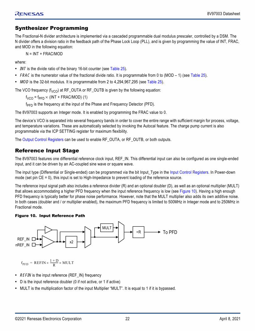
Feedback DividerThe feedback divider N supports fractional division capability in the PLL feedback path. It consists in an integer N divider of 16 bits, and a Fractional divider of 32 bits (FRAC) over 32-bits (MOD).
Figure 11. RF Feedback N Divider
The 16 INT bits (NInt[15:0] in the Feedback Divider Control Registers set the integer part of the feedback division ratio. The 32 FRAC bits (Bit NFrac[31:0] in the registers set the numerator of the fraction that goes into the Sigma Delta modulator. The 32 MOD bits (NMod[31:0] in the registers set the denominator of the fraction that goes into the Sigma Delta modulator.
From the relation (1), the VCO minimum step frequency is determined by (1/MOD) fPFD.
N Counter
16-bit INT
32-bit FRAC
32-bit MOD
3rd Order Modulator
From VCO Output To PFD
+
Σ

24©2021 Renesas Electronics Corporation April 8, 2021
8V97003 Datasheet
FRAC values from 0 to (MOD –1) cover channels over a frequency range equal to the PFD reference frequency. The PFD frequency is calculated as follows:
REFIN is the input reference (REF_IN) frequency
D is the input reference doubler (0 if not active, or 1 if active)
R is the 10-bit programmable input reference pre-divider
This formula assumes that the MULT input multiplier is bypassed.
The programmable modulus (MOD) is determined based on the input reference (REF_IN) frequency and the desired channelization (or output frequency resolution). The high resolution provided on the R counter and the Modulus allows the user to choose from several configuration of the PLL to optimize the performance. The high resolution Modulus also allows the use of the same input reference frequency to achieve different channelization requirements. Using a unique PFD frequency for several needed channelization requirements allows the user to design a loop filter for the different needed setups and ensure the stability of the loop.
The channelization is given by
In low noise mode (dither disabled), the Sigma Delta modulator can generate some fractional spurs that are due to the quantization noise. The spurs are located at regular intervals equal to fPFD/L where L is the repeat length of the code sequence in the Sigma Delta modulator. That repeat length depends on the MOD value, as described in Table 13.
In order to reduce the spurs, the user can enable the dither function to increase the repeat length of the code sequence in the Sigma Delta Modulator. The increased repeat length is 232 − 1 cycles so that the resulting quantization error is spread to appear like broadband noise. As a result, the in-band phase noise may be degraded when using the dither function. When the application requires the lowest possible phase noise and when the loop bandwidth is low enough to filter most of the undesirable spurs, or if the spurs will not affect the system performance, it is recommended to use the low noise mode with dither disabled.
Table 13. Fractional Spurs Due to the Quantization Noise
Condition (Dither Disabled) L Spur intervals
MOD can be divided by 2, but not by 3 2 MOD fPFD/(2 MOD)
MOD can be divided by 3, but not by 2 3 MOD fPFD/(3 MOD)
MOD can be divided by 6 6 MOD fPFD/(6 MOD)
Other conditions MOD fPFD/MOD (channel step)
fPFD REFIN1 D+
R-------------=
fPFD
MOD--------------
25©2021 Renesas Electronics Corporation April 8, 2021
8V97003 Datasheet
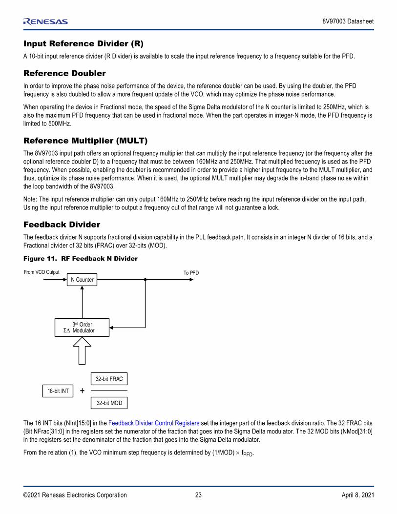
Phase and Frequency Detector (PFD) and Charge PumpThe phase detector compares the outputs from the R counter and N counter, and generates an output corresponding to the phase and frequency difference between the two inputs at the PFD. The charge pump current is programmable through the serial port (SPI) to several different levels (see Table 49).
Figure 12. Simplified PFD Circuit using D-type Flip-Flop
PFD FrequencyThe operating frequency for the PFD is up to 500MHz when the device operates in integer mode, and up to 250MHz when the device operates in fractional mode.
External Loop FilterThe 8V97003 requires an external loop filter. The design of that filter is application specific. For more information, see Applications Information.
Charge Pump High-ImpedanceIn order to put the charge pump into three-state mode, the user must set the bits CP_HiZ (Bit D5) to 1 in Register 47 in the Charge Pump Control Registers. This bit should be set to 0 for normal operation.
D1 Q1
VDD
REFIN [(1+D)/R] MULT
D1 Q1
FB
CPOUT
VDD
DELAY
ICP
ICP

26©2021 Renesas Electronics Corporation April 8, 2021
8V97003 Datasheet
Integrated Low Noise VCOThe VCO used in the 8V97003 is divided into several frequency bands. This allows for a lower VCO sensitivity (Kvco), which results in the best possible VCO phase noise and spurious performance.
The user does not have to select the different VCO bands. The VCO band select logic of the 8V97003 will automatically select the most suitable band of operation at power up or after programming. In addition, the Force_Relock bit (register 33, bit D7) can be used to automatically select the best frequency band.
Output Clock Distribution and Optional Output DoublerThe 8V97003 device provides two differential outputs. Either of the two outputs generates a frequency equal to fVCO when bypassing the optional output doubler and the optional output divider M0, or to 2 fVCO (up to 18GHz) when using the optional output doubler, or an integer division of the VCO frequency fVCO. The division ratios of the output divider are provided in the Output Control Registers.
Figure 13. Output Clock Distribution
RF_OUT and nRF_OUT are derived from the collector of an NPN differential pair driven by the VCO output (or the output doubler), as displayed in Figure 14.
Figure 14. Output Stage
The 8V97003 offers 4 bits of programmability for the RF output power of each output. The user can configure the RF output power to multiple available settings (see RF Output Power).
If the auxiliary output (RF_OUTB) is not used, it can be powered down by using the QB_ena bit in the Output Control Registers.
The outputs can be disabled until the part achieves lock. To enable this mode, the user will set the Mute_until_LD bit in the Outputs Control Registers (see Output Control Registers). The MUTE pin can be used to mute all outputs and be used as a similar function.
RF_OUTA
RF_OUTB
Mute Switches
nRF_OUTA
nRF_OUTB
x2
From VCO
/M0
RF_OUT nRF_OUT
VCO
or
Optional Output Doubler
Or
Optional Output Divider

27©2021 Renesas Electronics Corporation April 8, 2021
8V97003 Datasheet
Output MatchingThe outputs of the 8V97003 are “open collector outputs” and can be matched in different ways.
A simple resistive matching is used to terminate the open collector RF_OUT output with a 50Ω to VDD, and with an AC coupling capacitor in series. Two termination scheme examples are shown in Figure 15 and Figure 16. When considering the frequencies involved from the 8V97003, an inductively loaded configuration is recommended for better performance and optimal power transmission, and to minimize the distortion of the output signal. The resistive matching termination is not ideal to achieve maximum output power transmission, especially for high frequencies.
Figure 15. Resistive Matching Termination
This termination scheme provides one of the selected output powers on the differential pair when connected to a 50Ω load. For additional information about the output power selection, see RF Output Power.
The 50Ω resistor connected to VDD can also be replaced by a choke to provide better performance and optimal power transmission.
The pull-up inductor value is frequency dependent. For impedance matching of 50Ω, the inductance value can be calculated as L = 50 ÷ (2f), where “f” is the operating frequency. In this example, L = 1nH is for an operating frequency of approximately 6GHz.
Figure 16. Inductively Loaded Termination
For more recommendations on the termination scheme, see Applications Information.
Band Selection DisableFor a given frequency, the output phase can be adjusted when using the BandSelDisable bit (Bit D5 in Register 33; see Calibration Control Registers). When this bit is enabled (Bit D5 set to 1), the device does not complete a VCO band selection after changing the settings. When the Band_Sel_Disable bit is set to 0, and when the settings are updated, the device proceeds to a VCO band selection. The Band_Sel_Disable bit is useful when the user wants to make small changes in the output frequency (< 1MHz from the nominal frequency) without recalibrating the VCO and minimizing the settling time.
100
3.3V
Input Receiver
50
VDD
RF_OUT 100pF
3.3V
nRF_OUT
8V97003
100pF
Z0 = 50
Z0 = 50
50
100
3.3V
Input Receiver
1nH
VVCO
RF_OUT 100pF
3.3V
nRF_OUT
8V97003
100pF
1nH
Z0 = 50
Z0 = 50

28©2021 Renesas Electronics Corporation April 8, 2021
8V97003 Datasheet
Phase AdjustThe 8V97003 supports adjusting the phase delay between the outputs (RF_OUT/ nRF_OUT) and the input (REF_IN) of the device by shifting the output phase by a fraction of the size of the fractional denominator, when the device is used in fractional mode.
Writing to the Phase Adjustments Control Registers triggers a phase shift (see Table 28). The phase adjustment value set by the bits, Phase[31:0], should be less than the fractional-N denominator register, MOD. The actual phase shift can be obtained with the following equation:
or
360° represents one cycle of output clock, TVCO is the period of VCO (in ns), TOUT is the period at the output of the 8V97003, and Phase is a programmable value, the same bit length as MOD.
RF Output PowerEach output buffer RF_OUTA and RF_OUTB offers a configurable RF output power. The RF output power can be programmed via the bits RF_OUTA_pwr[3:0] and RF_OUTB_pwr[3:0] in the Output Control Registers.
Output Phase Synchronization
Input-to-OutputThe device input-to-output phase relations is deterministic with a fixed phase offset when the PLL feedback divider is integer and the output divider is not used. The phase offset remains the same across power cycles.
Output Phases of Multiple 8V97003 Devices The output phases of multiple devices can be aligned on the rising signal edge. This is supported for devices with identical configurations and the same input phase and frequency. The devices can use any setting of the input divider, input multiplier, integer and fractional feedback divider, the output frequency doubler, and the 1x frequency output path, but not the output divider.
Phase alignment across devices is established automatically when the PLL feedback divider is integer and the input frequency divider is not used.
In other configurations, an external pulse to the SYNC input establishes an output phase alignment. The SYNC pulse can be applied to the device at any time after the configuration is loaded with the AutoReSync register bit is set to 1 and the PLL is locked. Internal to the device, this synchronization procedure first resets the input divider and then resets the DSM. For applicable input SYNC and REF_IN timing requirements, see the following table.
Table 14. Timing Requirements
Symbol Parameter Test Conditions Minimum Maximum Unit
tS Setup TimeRising edge of SYNC pulse to Rising Edge of REF_IN
0.5 ns
tH Hold TimeRising Edge of REF_IN to Falling Edge of SYNC Pulse
0.5 ns
360PhaseMOD---------------
TVCO
TOUT--------------=Phase adjustment (degrees)
TVCOPhaseMOD--------------- =Phase adjustment (ns)

29©2021 Renesas Electronics Corporation April 8, 2021
8V97003 Datasheet
Power-Down ModeWhen power-down is activated, the following events occur:
1. VCO is not powered-down
2. RF_OUT buffers are disabled
3. The input stage is powered down and set to High-Impedance
4. Input registers remain active and capable of loading and latching data
5. The CE pin is set to low level (logic zero) for activating power-down mode. More power-down control bits are available in register 0x0028.
Default Power-Up ConditionsAll the RF outputs are muted at power-up. For default values in registers, see Register Map.
VCO CalibrationFor proper VCO calibration, the 8V97003 must be programmed with the following recommended settings:
The band select clock divider (Bits BndSelDiv[12:0] in the Band Select Clock Divider Control Registers) must be set to divide down the PFD frequency in between 50kHz to 100kHz (PFD Frequency/BandSelDiv[12:0] ≤ 100kHz and > 50kHz).
BandSelAcc[1:0] bits must be set to 10 or 11.
3- or 4-Wire SPI Interface DescriptionThe 8V97003 has a selectable 3/4-wire serial control port that can respond as a slave in an SPI configuration to allow read and write access to any of the internal registers for device programming or read back. The SPI interface consists of SCLK (clock), SDIO (serial data input and output in 3-wire mode, input in 4-wire mode), SDO (output in 4-wire mode), and CSB (chip select). A data transfer contains 16-bit instructions (direction +15 bit address) and any integer multiple of 8 bits data. Internal register data is organized in 8-bit byte.
3/4-Wire ModeThe 3- or 4-wire mode is defined by the SDO Active bit in the device configuration register 0x00 bit3 and bit4. If both bits are set to 0, the device is in a 3-wire mode and the SDIO pin is a bi-directional data input/ output, and the SDO pin is in high-impedance. Otherwise, the device is in a 4-wire mode, the SDIO pin is the data input, and the SDO pin is the data output.
Active Clock EdgeSDIO is always clocked-in on the rising edge of SCLK. SDIO (or SDO if in 4-wire mode) is always clocked-out on the falling edge of SCLK.
ResetAfter power-up or reset by the nRESET pin, the SPI engine is reset and all internal registers reset to their default values. The SPI interface is in 3-wire mode with SDO in high-impedance, MSB-first mode, and address is in auto-decrement mode.
The function of SoftReset bit in register 0x00 bit7 and bit0 is similar to the nRESET pin. It resets all the registers to their default values, except registers 0x00 and 0x01.

30©2021 Renesas Electronics Corporation April 8, 2021
8V97003 Datasheet
Least Significant Bit PositionThe 8V97003 supports both the least significant bit first and most significant bit first transfers.
If LSBFirst in register 0x00 bit6 and bit1 is set to 0, data is transferred in this order: transfer direction bit, the address bits A14 to A0, then first data byte D7 to D0, 2nd data byte D7 to D0, and so on until CSB is set to 1.
If LSBFirst is set to 1, the order is: address bits A0 to A14, then the transfer direction bit, then the first data byte D0 to D7, 2nd data byte D0 to D7, and so on until CSB is set to 1.
By default, LSBFirst is set to 0.
AddressingThe 8V97003 implements registers at the addresses from 0x00 to 0x49. The addressing mode is 15-bit.
During transferring operation, address increments automatically if AddressAcend in register 0x00 bit5 and bit2 is set to 1; otherwise it decrements. In incrementing mode, if address reaches 0x49, it wrap-around to 0x00. In decrementing mode, if address reaches 0x00, it wrap-around to 0x49.
By default, decrementing mode is set.
Read OperationA SPI operation starts when there is a high to low transition on CSB, and stops when there is a low to high transition on CSB. If the transfer direction bit R/nW is 1, it is a read operation; otherwise it is a write operation.
This device supports multi-byte read or write operations. Bits A14 to A0 refer to the register address. The device reads or writes data to this address and continues as long as CSB is held at low. The device automatically increments or decrements the address depending on AddressAcend bit.
Figure 17 to Figure 22 show the operation protocols.
Mirrored Register BitsIn register 0x00, bits D7–D4 are mirrored with the bits D3–D0. The mirrored bits pair must set to the same value.
Double-Buffered RegistersConfiguration registers that are wider than 8 bits are double-buffered for synchronous access. For these registers, it is required to write the multiple-byte setting into the buffered registers first. The new configurations will not take effect until writing 1 to the TransferOn bit in register 0x0F bit0 to transfer them from the buffered registers to the active registers. TransferOn bit is self-clearing. Multiple-byte configuration data can be read-back either from buffered registers or active registers as specified by the BufferReadMode bit in register 0x01 bit5.
Register 0x10 to 0x1D, 0x22 to 0x25, and 0x29 to 0x2C are double buffered.

31©2021 Renesas Electronics Corporation April 8, 2021
8V97003 Datasheet
Operation ProtocolsFigure 17. 4-Wire MSB First, Single Byte Write and Read
nCS
SCLK
SDIO
Single-byte data write
D1D2D3 D0D4D5D6D7A1 A0A2A3A4A5A6A7A8A9A10A11A12R/W
Instruction Reg( n) Data
nCS
SCLK
SDIO
Single-byte data readback
D1D2D3 D0D4D5D6D7
A1 A0A2A3A4A5A6A7A8A9A10A11A12A13A14R/W
Instruction
Reg( n) Data
SDO
A13A14
CSB
CSB
Register Address
Register Address
Register
Register
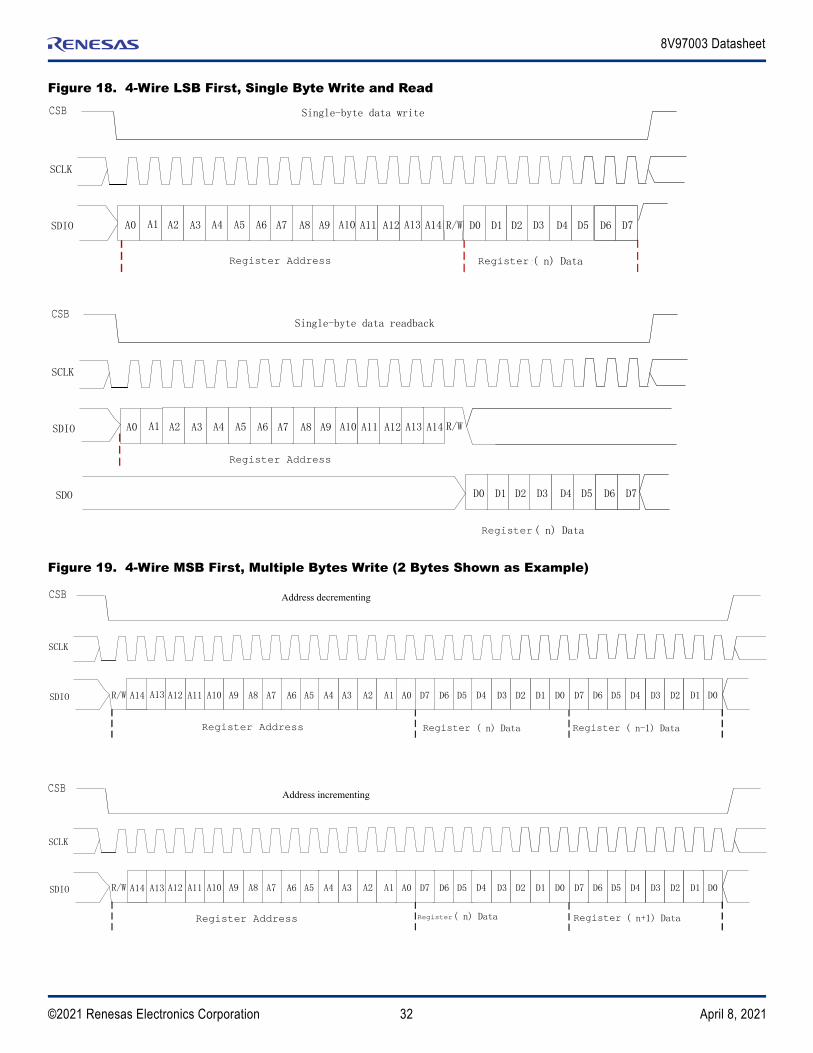
32©2021 Renesas Electronics Corporation April 8, 2021
8V97003 Datasheet
Figure 18. 4-Wire LSB First, Single Byte Write and Read
Figure 19. 4-Wire MSB First, Multiple Bytes Write (2 Bytes Shown as Example)
nCS
SCLK
SDIO
Single-byte data write
R/W
Instruction Reg( n) Data
nCS
SCLK
SDIO
Single-byte data readback
R/W
Instruction
Reg( n) Data
SDO
A13 A14A12A11A10A9A8A7A6A5A4A3A2A1A0 D6D5D4 D7D3D2D1D0
D6D5D4 D7D3D2D1D0
A13 A14A12A11A10A9A8A7A6A5A4A3A2A1A0
CSB
CSB
Register Address
Register Address
Register
Register
nCS
SCLK
SDIO
Address decrementing
D0D1D2D3D4D5D6D7D1D2D3 D0D4D5D6D7A1 A0A2A3A4A5A6A7A8A9A10A11A12A13A14R/W
Instruction Reg( n) Data Reg( n-1) Data
nCS
SCLK
SDIO
Address incrementing
D0D1D2D3D4D5D6D7D1D2D3 D0D4D5D6D7A1 A0A2A3A4A5A6A7A8A9A10A11A12R/W
Instruction Reg( n) Data Reg( n+1) Data
A13A14
CSB
CSB
Register Address
Register Address
Register
Register
Register
Register

33©2021 Renesas Electronics Corporation April 8, 2021
8V97003 Datasheet
Figure 20. 4-Wire LSB First, Multiple Bytes Read (2 Bytes Shown as Example)
Figure 21. 3-Wire MSB First, Single Byte Read and Write
nCS
SCLK
SDIO
Address decrementing
A1 A0A2A3A4A5A6A7A8A9A10A11A12A13A14R/W
nCS
SCLK
Address incrementing
SDIO D0D1D2D3D4D5D6D7D1D2D3 D0D4D5D6D7
Instruction Reg(n)Data Reg(n‐1)Data
SDIO A1 A0A2A3A4A5A6A7A8A9A10A11A12A13A14R/W
SDIO D0D1D2D3D4D5D6D7D1D2D3 D0D4D5D6D7
Instruction Reg(n)Data Reg(n+1)Data
CSB
CSB
Register Address
Register Address
Register
Register
Register
Register
SDO
SDO
nCS
SCLK
SDIO D1D2D3 D0D4D5D6D7A1 A0A2A3A4A5A6A7A8A9A10A11A12A13A14R/W
Instruction Reg( n) Data
CSB
Register Address Register

34©2021 Renesas Electronics Corporation April 8, 2021
8V97003 Datasheet
Figure 22. SPI Timing Diagram
Table 15. SPI Read / Write Cycle Timing Parameters
Parameter Minimum Maximum Units
fSCLK SCLK Frequency 20 MHz
tpwh SCLK High Pulse Width 25 ns
tpwl SCLK Low Pulse Width 25 ns
tS1 Setup Ttime, CSB falling to SCLK rising 10 ns
th1 Hold Time, SCLK falling to CSB rising 30 ns
tS2 Setup Time, SDIO input edge to SCLK rising 8 ns
th2 Hold Time, SCLK rising to SDIO input edge 8 ns
td1SCLK Falling Edge to valid readback data on SDIO if in 3-wire mode, or SDO if in 4-wire mode
10 ns
td2CSB Rising Edge to High-Impedance on SDIO if in 3-wire mode, or SDO if in 4-wire mode
10 ns
nCS
SCLK
SDIO
ts1
R/W
SDO
A0
ts2
tpwh tpwl th1
td1Hi‐z Hi‐z
td2
th2
A1
D0 D1
CSB

35©2021 Renesas Electronics Corporation April 8, 2021
8V97003 Datasheet
Register MapTable 16. Preface Registers
Register Addr TypeDefault Value D7 D6 D5 D4 D3 D2 D1 D0
0 0000 R/W 0000_0000 SoftReset LSBFirst AddressAscend
SDOActive SDOActive AddressAscend
LSBFirst SoftReset
1 0001 R/W 0000_0000 Unused Unused BufferReadMode
Unused Unused Unused Unused Unused
2 0002 R/W 0000_0000 Unused Unused Unused Unused Unused Unused Unused Unused
3 0003 R 0000_0110 ChipType<7> ChipType<6> ChipType<5> ChipType<4> ChipType<3> ChipType<2> ChipType<1> ChipType<0>
4 0004 R 0000_0000 ChipID<7> ChipID<6> ChipID<5> ChipID<4> ChipID<3> ChipID<2> ChipID<1> ChipID<0>
5 0005 R 0000_0000 ChipID<15> ChipID<14> ChipID<13> ChipID<12> ChipID<11> ChipID<10> ChipID<9> ChipID<8>
6 0006 R 0000_0000 ChipVersion<7>
ChipVersion<6>
ChipVersion<5>
ChipVersion<4>
ChipVersion<3>
ChipVersion<2>
ChipVersion<1>
ChipVersion<0>
7 0007 R 0001_0001 ChipOption<7>
ChipOption<6>
ChipOption<5>
ChipOption<4>
ChipOption<3>
ChipOption<2>
ChipOption<1>
ChipOption<0>
8 0008 R/W 0000_0000 Unused Unused Unused Unused Unused Unused Unused Unused
9 0009 R/W 0000_0000 Unused Unused Unused Unused Unused Unused Unused Unused
10 000A R/W 0000_0000 Unused Unused Unused Unused Unused Unused Unused Unused
11 000B R/W 0000_0000 Unused Unused Unused Unused Unused Unused Unused Unused
12 000C R 0010_0110 VendorID<7> VendorID<6> VendorID<5> VendorID<4> VendorID<3> VendorID<2> VendorID<1> VendorID<0>
13 000D R 0000_0100 VendorID<15> VendorID<14> VendorID<13> VendorID<12> VendorID<11> VendorID<10> VendorID<9> VendorID<8>
14 000E R/W 0000_0000 Unused Unused Unused Unused Unused Unused Unused Unused
15 000F R/W 0000_0000 Unused Unused Unused Unused Unused Unused Unused TransferOn
Table 17. Control Registers[a]
Register Addr TypeDefault Value D7 D6 D5 D4 D3 D2 D1 D0
16 0010 R/W 0001_1111 NInt<7> NInt<6> NInt<5> NInt<4> NInt<3> NInt<2> NInt<1> NInt<0>
17 0011 R/W 0000_0000 NInt<15> NInt<14> NInt<13> NInt<12> NInt<11> NInt<10> NInt<9> NInt<8>
18 0012 R/W 1000_0110 NFrac<7> NFrac<6> NFrac<5> NFrac<4> NFrac<3> NFrac<2> NFrac<1> NFrac<0>
19 0013 R/W 1111_1110 NFrac<15> NFrac<14> NFrac<13> NFrac<12> NFrac<11> NFrac<10> NFrac<9> NFrac<8>
20 0014 R/W 1111_1111 NFrac<23> NFrac<22> NFrac<21> NFrac<20> NFrac<19> NFrac<18> NFrac<17> NFrac<16>
21 0015 R/W 1011_1100 NFrac<31> NFrac<30> NFrac<29> NFrac<28> NFrac<27> NFrac<26> NFrac<25> NFrac<24>
22 0016 R/W 0000_0000 NMod<7> NMod<6> NMod<5> NMod<4> NMod<3> NMod<2> NMod<1> NMod<0>
23 0017 R/W 1111_1110 NMod<15> NMod<14> NMod<13> NMod<12> NMod<11> NMod<10> NMod<9> NMod<8>
24 0018 R/W 1111_1111 NMod<23> NMod<22> NMod<21> NMod<20> NMod<19> NMod<18> NMod<17> NMod<16>
25 0019 R/W 1111_1111 NMod<31> NMod<30> NMod<29> NMod<28> NMod<27> NMod<26> NMod<25> NMod<24>
26 001A R/W 0000_0001 Phase<7> Phase<6> Phase<5> Phase<4> Phase<3> Phase<2> Phase<1> Phase<0>
27 001B R/W 0000_0000 Phase<15> Phase<14> Phase<13> Phase<12> Phase<11> Phase<10> Phase<9> Phase<8>

36©2021 Renesas Electronics Corporation April 8, 2021
8V97003 Datasheet
28 001C R/W 0000_0000 Phase<23> Phase<22> Phase<21> Phase<20> Phase<19> Phase<18> Phase<17> Phase<16>
29 001D R/W 0000_0000 Phase<31> Phase<30> Phase<29> Phase<28> Phase<27> Phase<26> Phase<25> Phase<24>
30 001E R/W 0111_0010 0 DSMOrder<2>
DSMOrder<1>
DSMOrder<0>
DitherG<1> DitherG<0> ShapeDitherEn
DitherEn
31 001F R/W 0000_1000 ManualBandEn
0 0 0 VCOManu<3>
VCOManu<2>
VCOManu<1>
VCOManu<0>
32 0020 R/W 0100_0000 Unused BandManu<6>
BandManu<5>
BandManu<4>
BandManu<3>
BandManu<2>
BandManu<1>
BandManu<0>
33 0021 R/W 0000_0011 ForceRelock
PhAdj BandSelDisable
ManualReSync
0 0 BandSelAcc<1>
BandSelAcc<0>
34 0022 R/W 0000_0000 BndSelDiv<7>
BndSelDiv<6>
BndSelDiv<5>
BndSelDiv<4>
BndSelDiv<3>
BndSelDiv<2>
BndSelDiv<1>
BndSelDiv<0>
35 0023 R/W 0000_1010 Unused Unused Unused BndSelDiv<12>
BndSelDiv<11>
BndSelDiv<10>
BndSelDiv<9>
BndSelDiv<8>
36 0024 R/W 0000_0000 1 0 0 0 0 0 0 0
37 0025 R/W 0000_0000 0 0 0 0 0 0 0 0
38 0026 R/W 0000_0000 Unused Unused Unused LD_Enable AutoRecalEn
0 0 0
39 0027 R/W 0000_0000 Unused Unused LDPinMode<1>
LDPinMode<0>
Unused LDP<2> LDP<1> LDP<0>
40 0028 R/W 0000_0001 Reserved ref_vreg_pwrdwn
pdcp_vreg_pwrdwn
fb_vreg_pwrdwn
outA_vreg_pwrdwn
outBbuf_vreg_pwrdwn
PDNAnaRegu
VCO_En
41 0029 R/W 0000_0001 R<7> R<6> R<5> R<4> R<3> R<2> R<1> R<0>
42 002A R/W 0000_1100 Unused Unused Unused RefDoubler_Delay
Input_Type RefDoubler_En
R<9> R<8>
43 002B R/W 0000_0000 Mult_En Mult_reset Mult<5> Mult<4> Mult<3> Mult<2> Mult<1> Mult<0>
44 002C R/W 0000_0000 nMultpwrdwn<2>
nMultpwrdwn<1>
nMultpwrdwn<0>
Mult_force_vchi
Mult_force_vclow
1 0 0
45 002D R/W 0001_1101 Unused Unused Icp_pmos<5>
Icp_pmos<4>
Icp_pmos<3>
Icp_pmos<2>
Icp_pmos<1>
Icp_pmos<0>
46 002E R/W 0001_1101 Unused Unused Icp_nmos<5>
Icp_nmos<4>
Icp_nmos<3>
Icp_nmos<2>
Icp_nmos<1>
Icp_nmos<0>
47 002F R/W 0000_0000 CP_HiZ Icp_bleeder<6>
Icp_bleeder<5>
Icp_bleeder<4>
Icp_bleeder<3>
Icp_bleeder<2>
Icp_bleeder<1>
Icp_bleeder<0>
48 0030 R/W 0110_0010 Unused Unused Unused Unused pfd_pw<1> pfd_pw<0> 1 Unused
49 0031 R/W 0000_0000 1 0 0 0 1 0 0 0
50 0032 R/W 0000_0000 AutoReSync
0 0 1 0 0 1 1
51 0033 R/W 0000_0000 Unused Unused Unused Unused RF_OUTA_pwr<3>
RF_OUTA_pwr<2>
RF_OUTA_pwr<1>
RF_OUTA_pwr<0>
52 0034 R/W 0000_1000 1 Unused Mute_until_LD
RF_OUTA_ena
1 1 1 0
53 0035 R/W 0000_0000 Unused Unused Unused Unused RF_OUTB_pwr<3>
RF_OUTB_pwr<2>
RF_OUTB_pwr<1>
RF_OUTB_pwr<0>
Table 17. Control Registers[a] (Cont.)
Register Addr TypeDefault Value D7 D6 D5 D4 D3 D2 D1 D0

37©2021 Renesas Electronics Corporation April 8, 2021
8V97003 Datasheet
54 0036 R/W 0000_1000 1 Unused Unused RF_OUTB_ena
1 1 1 0
55 0037 R/W 0000_0000 Reserved Reserved Reserved Reserved Reserved Reserved Reserved Reserved
56 0038 R/W 0000_0000 Reserved Reserved Reserved Reserved Reserved Reserved Reserved Reserved
57 0039 R/W 0000_0000 Reserved Reserved Reserved Reserved Reserved Reserved Reserved Reserved
58 003A R/W 0000_0000 Reserved Reserved Reserved Reserved Reserved Reserved Reserved Reserved
59 003B R/W 0000_0000 OutDoubler_Ena
OutDivider_Ena
OutDoubler_Freq
Unused Unused OutDiv<2> OutDiv<1> OutDiv<0>
60 003C R/W 0000_0000 Unused Unused Unused Unused 0 0 1 0
61 003D R/W 0000_0000 Unused Unused Unused Reserved Reserved 0 0 0
62 003E R/W 0000_0000 Unused Unused Unused Unused Unused Unused Unused Unused
63 003F R/W 0000_0000 Unused Unused Unused Unused Unused Unused Unused Reserved
64 0040 R/W 0000_0000 Reserved Reserved Reserved Reserved Reserved Reserved Reserved Reserved
65 0041 R/W 0110_0010 0 1 1 0 Unused Unused 1 0
66 0042 R/W 0010_0010 Unused Unused 1 0 Unused Unused 1 0
67 0043 R/W 0010_0010 Unused Unused 1 0 Unused Unused 1 0
[a] It is recommended to write 0 for Unused and Reserved bits when writing.
Table 18. Status Registers
Register Addr TypeDefault Value D7 D6 D5 D4 D3 D2 D1 D0
68 0044 R 0000_0000 DigLock BandSelDone
Unused Unused VcoSts<3> VcoSts<2> VcoSts<1> VcoSts<0>
69 0045 R 0000_0000 Unused BandSts<6> BandSts<5> BandSts<4> BandSts<3> BandSts<2> BandSts<1> BandSts<0>
70 0046 R 0000_0000 0 0 0 0 0 0 0 0
71 0047 R 0000_0000 Unused Unused 0 0 0 0 0 0
72 0048 R 0000_0000 Unused Unused Unused Unused Unused Unused Unused Unused
73 0049 R/W 0000_0000 Unused Unused Unused Unused Unused LossLock Unused Unused
Table 17. Control Registers[a] (Cont.)
Register Addr TypeDefault Value D7 D6 D5 D4 D3 D2 D1 D0

38©2021 Renesas Electronics Corporation April 8, 2021
8V97003 Datasheet
Register Block DescriptionsTable 19. Register Block Descriptions
Register Blocks (Hex) Register Block Descriptions
Pref
ace
Reg
iste
rs
0000–0001 Startup Control Registers
0002 Reserved
0003–0007 Device Type, ID Version, and Option Registers
0008–000B Unused
000C–000D Vendor ID Control Registers
000E–000F Unused
Con
trol
Reg
iste
rs
0010–0019 Feedback Divider Control Registers
001A–001D Phase Adjustments Control Registers
001E DSM Control Registers
001F–0020 Manual VCO and Digital Band Selection
0021 Calibration Control Registers
0022–0023 Band Select Clock Divider Control Registers
0024–0025 Reserved
0026–0027 Lock Detect Control Registers
0028 Power Down Control Registers
0029–002C Input Control Registers
002D–002F Charge Pump Current Control Registers
0030 PFD Pulse Width Control Registers
0031–0032 Re-Sync Control Registers
0033–003B Output Control Registers
003C Reserved
003D Reserved
003E–0040 Unused or Reserved
0041–0043 Reserved
Stat
usR
egis
ters
0044 Digital Lock and Calibration and VCO Status Registers
0045 Digital Band Status Registers
0046–0048 Reserved or Unused
0049 Loss of Lock Status Registers

39©2021 Renesas Electronics Corporation April 8, 2021
8V97003 Datasheet
Preface RegistersTable 20. Preface Register Block
Register Blocks (Hex) Register Block Descriptions
0000–0001 Startup Control Registers
0002 Reserved
0003–0006 Device Type, ID and Version Registers
0007 Reserved
0008–000B Unused
000C 000D Vendor ID Control Registers
000E–000F Unused
Table 21. Preface Register Bits
Addr D7 D6 D5 D4 D3 D2 D1 D0
0000 SoftReset LSBFirst AddressAscend SDOActive <SDOActive> <AddressAscend> <LSBFirst> <SoftReset>
0001 Unused Unused BufferReadMode Unused Unused Unused Unused Unused
0002 Unused Unused Unused Unused Unused Unused Unused Unused
0003 ChipType<7> ChipType<6> ChipType<5> ChipType<4> ChipType<3> ChipType<2> ChipType<1> ChipType<0>
0004 ChipID<7> ChipID<6> ChipID<5> ChipID<4> ChipID<3> ChipID<2> ChipID<1> ChipID<0>
0005 ChipID<15> ChipID<14> ChipID<13> ChipID<12> ChipID<11> ChipID<10> ChipID<9> ChipID<8>
0006 ChipVersion<7> ChipVersion<6> ChipVersion<5> ChipVersion<4> ChipVersion<3> ChipVersion<2> ChipVersion<1> ChipVersion<0>
0007 ChipOption<7> ChipOption<6> ChipOption<5> ChipOption<4> ChipOption<3> ChipOption<2> ChipOption<1> ChipOption<0>
0008 Unused Unused Unused Unused Unused Unused Unused Unused
0009 Unused Unused Unused Unused Unused Unused Unused Unused
000A Unused Unused Unused Unused Unused Unused Unused Unused
000B Unused Unused Unused Unused Unused Unused Unused Unused
000C VendorID<7> VendorID<6> VendorID<5> VendorID<4> VendorID<3> VendorID<2> VendorID<1> VendorID<0>
000D VendorID<15> VendorID<14> VendorID<13> VendorID<12> VendorID<11> VendorID<10> VendorID<9> VendorID<8>
000E Unused Unused Unused Unused Unused Unused Unused Unused
000F Unused Unused Unused Unused Unused Unused Unused TransferOn

40©2021 Renesas Electronics Corporation April 8, 2021
8V97003 Datasheet
Table 22. Preface Register Description
Bit Field Name Field Type Default (Binary) Description
SoftReset<SoftReset>
R/WAuto-Clear
0
Soft Reset Function:
0 = Normal operation
1 = Register reset. The device loads the default values into the registers, 0002 - 0049.
The content of the register addresses 0000 an 0001 and the SPI engine are not reset.
SoftReset bit D7 is mirrored with <SoftReset> in bit position D0. Register reset requires setting both SoftReset and <SoftReset> bits.
LSBFirst<LSBFirst>
R/W 0
Least Significant Bit Position:
Defines the bit transmitted first in SPI transfers between slave and master.
0 = The most significant bit (D7) first
1 = The least significant bit (D0) first
The LSBFirst bit D6 is mirrored with the <LSBFirst> in bit position D1. Changing LSBFirst to most significant bit requires setting both LSBFirst and <LSBFirst> bits.
AddressAscend<AddressAscend>
R/W 0
Address Ascend On:
0 = Address Ascend is off (addresses auto-decrement in streaming SPI mode)
1 = Address Ascend is on (addresses auto-increment in streaming SPI mode)
The AddressAscend bit specifies whether addresses are incremented or decremented in streaming SPI transfers.
The AddressAscend bit D5 is mirrored with the <AddressAscend> in bit position D2. Changing AddressAscend to “ON” requires setting both the AddressAscend and <AddressAscend> bits.
SDOActive<SDOActive>
R/W 0
SPI 3/4-Wire Mode:
Selects the unidirectional or bidirectional data transfer mode for the SDIO pin.
0 = SPI 3-wire mode:– SDIO is the SPI bidirectional data I/O pin– SDO pin is not used and is in high-impedance
1 = SPI 4-wire mode
– SDIO is the SPI data input pin– SDO is the SPI data output pin
The SDOActive bit D4 is mirrored with <SDOActive> in bit position D3. Changing SDOActive to SPI 4-wire mode requires setting both the SDOActive and <SDOActive> bits.
BufferReadMode R/W 0
Read Back Mode of the Buffer Registers:
0 = Read from active registers
1 = Read from the Buffer Register (case of Doubled Buffer Registers); If the register being read is not doubled buffered, a 1 value will read from the active register.
ChipType[7:0] R only 0000 0110Device (Chip) Type:
Reads 00000110 (RF Synthesizer / PLL) after power-up and reset.
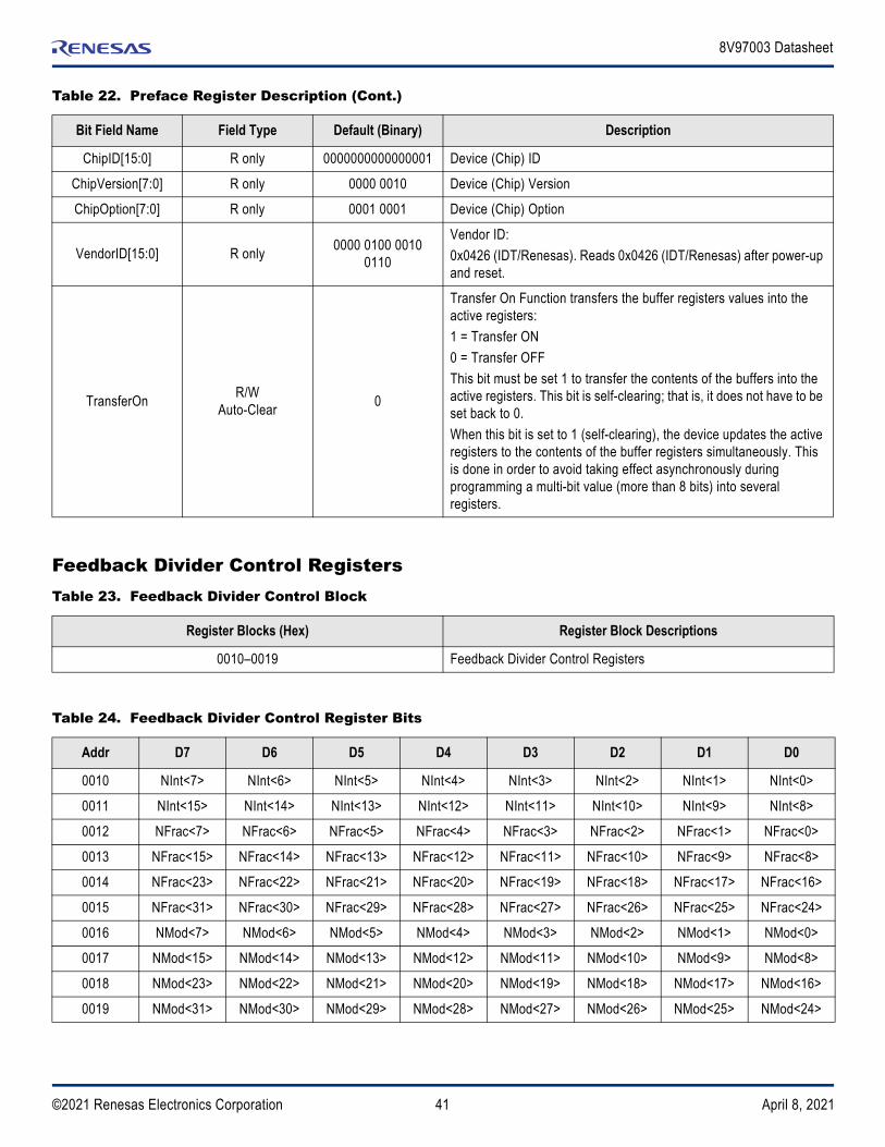
41©2021 Renesas Electronics Corporation April 8, 2021
8V97003 Datasheet
Feedback Divider Control Registers
ChipID[15:0] R only 0000000000000001 Device (Chip) ID
ChipVersion[7:0] R only 0000 0010 Device (Chip) Version
ChipOption[7:0] R only 0001 0001 Device (Chip) Option
VendorID[15:0] R only0000 0100 0010
0110
Vendor ID:
0x0426 (IDT/Renesas). Reads 0x0426 (IDT/Renesas) after power-up and reset.
TransferOnR/W
Auto-Clear0
Transfer On Function transfers the buffer registers values into the active registers:
1 = Transfer ON
0 = Transfer OFF
This bit must be set 1 to transfer the contents of the buffers into the active registers. This bit is self-clearing; that is, it does not have to be set back to 0.
When this bit is set to 1 (self-clearing), the device updates the active registers to the contents of the buffer registers simultaneously. This is done in order to avoid taking effect asynchronously during programming a multi-bit value (more than 8 bits) into several registers.
Table 23. Feedback Divider Control Block
Register Blocks (Hex) Register Block Descriptions
0010–0019 Feedback Divider Control Registers
Table 24. Feedback Divider Control Register Bits
Addr D7 D6 D5 D4 D3 D2 D1 D0
0010 NInt<7> NInt<6> NInt<5> NInt<4> NInt<3> NInt<2> NInt<1> NInt<0>
0011 NInt<15> NInt<14> NInt<13> NInt<12> NInt<11> NInt<10> NInt<9> NInt<8>
0012 NFrac<7> NFrac<6> NFrac<5> NFrac<4> NFrac<3> NFrac<2> NFrac<1> NFrac<0>
0013 NFrac<15> NFrac<14> NFrac<13> NFrac<12> NFrac<11> NFrac<10> NFrac<9> NFrac<8>
0014 NFrac<23> NFrac<22> NFrac<21> NFrac<20> NFrac<19> NFrac<18> NFrac<17> NFrac<16>
0015 NFrac<31> NFrac<30> NFrac<29> NFrac<28> NFrac<27> NFrac<26> NFrac<25> NFrac<24>
0016 NMod<7> NMod<6> NMod<5> NMod<4> NMod<3> NMod<2> NMod<1> NMod<0>
0017 NMod<15> NMod<14> NMod<13> NMod<12> NMod<11> NMod<10> NMod<9> NMod<8>
0018 NMod<23> NMod<22> NMod<21> NMod<20> NMod<19> NMod<18> NMod<17> NMod<16>
0019 NMod<31> NMod<30> NMod<29> NMod<28> NMod<27> NMod<26> NMod<25> NMod<24>
Table 22. Preface Register Description (Cont.)
Bit Field Name Field Type Default (Binary) Description

42©2021 Renesas Electronics Corporation April 8, 2021
8V97003 Datasheet
Table 25. Feedback Divider Control Register Description
Register Description
Bit Field Name Field Type Default (Binary) Description
Nint[15:0] R/W 0000 0000 0001 1111 = d'31
PLL Feedback Divider N Integer Portion INT:
Minimum divide ratio is 12
0000 0000 0000 0000 = Not allowed
…
0000 0000 0000 1011 = Not allowed
0000 0000 0000 0111 = 12
…
0000 0000 0001 1111 = 31 (default)
…
1111 1111 1111 1111 = 65,535
Nfrac[31:0] R/W 1011 1100 1111 1111 1111 1110 1000 0110
= d'3,170,893,446
PLL Feedback Divider N Fractional Portion FRAC [a]:
0000 0000 0000 0000 0000 0000 0000 0000 = d'0
…
1011 1100 1111 1111 1111 1110 1000 0110 = d'3,170,893,446 (default)
…
1111 1111 1111 1111 1111 1111 1111 1111 = d'4,294,967,295
Nmod[31:0] R/W 1111 1111 1111 1111 1111 1110 0000 0000
= d'4,294,966,784
PLL Feedback Divider N Modulus Portion MOD:
0000 0000 0000 0000 0000 0000 0000 0000 = Not allowed
0000 0000 0000 0000 0000 0000 0000 0001 = Not allowed
0000 0000 0000 0000 0000 0000 0000 0010 = d'2
…
1111 1111 1111 1111 1111 1110 0000 0000 = d'4,294,966,784 (default)
…
1111 1111 1111 1111 1111 1111 1111 1111 = d'4,294,967,295
[a] Nfrac is the numerator value of the fractional divide ratio. It is programmable from 0 to (MOD −1).

43©2021 Renesas Electronics Corporation April 8, 2021
8V97003 Datasheet
Phase Adjustments Control RegistersTable 26. Phase Adjustments Control Register Block
Register Blocks (Hex) Register Block Descriptions
001A–001D Phase Adjustments Control Registers
Table 27. Phase Adjustments Control Register Bits
Addr D7 D6 D5 D4 D3 D2 D1 D0
001A Phase<7> Phase<6> Phase<5> Phase<4> Phase<3> Phase<2> Phase<1> Phase<0>
001B Phase<15> Phase<14> Phase<13> Phase<12> Phase<11> Phase<10> Phase<9> Phase<8>
001C Phase<23> Phase<22> Phase<21> Phase<20> Phase<19> Phase<18> Phase<17> Phase<16>
001D Phase<31> Phase<30> Phase<29> Phase<28> Phase<27> Phase<26> Phase<25> Phase<24>
Table 28. Phase Adjustments Control Register Descriptions
Register Description
Bit Field Name Field Type Default (Binary) Description
Phase[31:0] R/W 0000 0000 0000 0000 0000 0000 0000 0001 = d'1
Phase Adjustments[a]
0000 0000 0000 0000 0000 0000 0000 0000 = d'0
0000 0000 0000 0000 0000 0000 0000 0001 = d'1 (default)
…
1111 1111 1111 1111 1111 1111 1111 1111 = d'4,294,967,295
[a] Phase adjustment (Phase value) must be less than the Modulus (Nmod value).

44©2021 Renesas Electronics Corporation April 8, 2021
8V97003 Datasheet
DSM Control RegistersTable 29. DSM Control Register Block
Register Blocks (Hex) Register Block Descriptions
001E DSM Control Registers
Table 30. DSM Control Register Bits
Addr D7 D6 D5 D4 D3 D2 D1 D0
001E 0 DSMOrder<2> DSMOrder<1> DSMOrder<0> DitherG<1> DitherG<0> ShapeDitherEn DitherEn
Table 31. DSM Control Register Descriptions
Register Description
Bit Field Name Field Type Default (Binary) Description
DSMOrder[2:0] R/W 111 DSM Order
000 = OFF. The device operates in integer mode and the fractional part is ignored
001 = 1st order
010 = 2nd order
011 = 3rd order
100 = Reserved
101 = Reserved
110 = Reserved
111 = 3rd order (default)
DitherG[1:0] R/W 00 Dither Gain
00 = LSB Dither (Recommended) (default)
01 = LSB x2 Dither
10 = LSB x4 Dither
11 = LSB x8 Dither
ShapeDitherEn R/W 1 Shape Dither Enable
0 = Shaped dither disabled
1 = Shaped dither enabled
DitherEn R/W 0 Dither Enable
0 = Dither off
1 = Dither on

45©2021 Renesas Electronics Corporation April 8, 2021
8V97003 Datasheet
Calibration Control RegistersTable 32. Calibration Control Register Block
Register Blocks (Hex) Register Block Descriptions
001F–0021 Calibration Control Registers
Table 33. Calibration Control Register Bits
Addr D7 D6 D5 D4 D3 D2 D1 D0
001F ManuBandEn 0 0 0 VCOManu<3> VCOManu<2> VCOManu<1> VCOManu<0>
0020 0 BandManu<6> BandManu<5> BandManu<4> BandManu<3> BandManu<2> BandManu<1> BandManu<0>
0021 ForceRelock PhAdj BandSelDisable ManualReSync 0 0 BandSelAcc<1> BandSelAcc<0>
Table 34. Calibration Control Register Descriptions
Register Description
Bit Field Name Field Type Default (Binary) Description
ManuBandEn R/W 0 Calibration Mode Enable
0 = Automatic VCO and Digital Band Selection
1 = Manual VCO and Digital Band Selection
VCOManu[3:0] R/W 1000 Manual VCO Selection (when ManuBandEn=1)
0000 = VCO0
0001= VCO1
...
0111 = VCO7
1000 – 1111 = Unused
Bandmanu[6:0] R/W 10000000 Manual Digital Band Selection (when ManuBandEn=1)
0000000 = Band
0000001 = Band1
...
1111111 = Band127
ForceRelock R/W 0 ForceRelock
0 = Normal operation (default)
1 = VCO forced to recalibrate. This bit is self-clearing.
Note: When the PLL is used in integer mode, this bit must be set to 1 after programming the feedback divider value.
PhAdj R/W 0 Phase Adjust Triggers
0 = Normal operation
1 = Trigger phase adjustment once. This bit is self-clearing.

46©2021 Renesas Electronics Corporation April 8, 2021
8V97003 Datasheet
Band Select Clock Divider Control Registers
BandSelDisable R/W 0 Band Select Disable
This bit will prevent a VCO recalibration when registers 0x0010 - 0x0019 are written.
0 = VCO recalibrates when registers 0x0010 - 0x0019 are written
1 = VCO does not recalibrate when registers 0x0010 - 0x0019 are written
ManualReSync R/W 0 0 = Normal operation
1 = Reset the DSM immediately
BandSelAcc[1:0] R/W 11 Band select/Calibration resolution
00 = Reserved
01 = Reserved
10 = 4x resolution
11 = 8x resolution (default)
Table 35. Band Select Clock Divider Control Register Block
Register Blocks (Hex) Register Block Descriptions
0022–0023 Band Select Clock Divider Control Registers
Table 36. Band Select Clock Divider Control Register Bits
Addr D7 D6 D5 D4 D3 D2 D1 D0
0022 BndSelDiv<7> BndSelDiv<6> BndSelDiv<5> BndSelDiv<4> BndSelDiv<3> BndSelDiv<2> BndSelDiv<1> BndSelDiv<0>
0023 Unused Unused Unused BndSelDiv<12> BndSelDiv<11> BndSelDiv<10> BndSelDiv<9> BndSelDiv<8>
Table 37. Band Select Clock Divider Control Register Descriptions
Register Description
Bit Field Name Field Type Default (Binary) Description
BndSelDiv[12:0] R/W 0 1010 0000 0000= d'2,560
Band Select Clock Divider[a]
0 0000 0000 0000 = Not allowed
0 0000 0000 0001 = d'1
…
0 1010 0000 0000 = d'2,560 (default)
…
1 1111 1111 1111 = d'8,192
[a] This value should be set so that FPFD / BndSelDiv is < 100kHz and > 50kHz.
Table 34. Calibration Control Register Descriptions
Register Description
Bit Field Name Field Type Default (Binary) Description

47©2021 Renesas Electronics Corporation April 8, 2021
8V97003 Datasheet
Lock Detect Control RegistersTable 38. Lock Detect Control Register Block
Register Blocks (Hex) Register Block Descriptions
0026–0027 Lock Detect Control Registers
Table 39. Lock Detect Control Register Bits
Addr D7 D6 D5 D4 D3 D2 D1 D0
0026 Unused Unused Unused LD_Disable AutoRecalEn 0 0 0
0027 Unused Unused LDPinMode<1> LDPinMode<0> Unused LDP<2> LDP<1> LDP<0>
Table 40. Lock Detect Control Register Descriptions
Register Description
Bit Field Name Field Type Default (Binary) Description
LD_Disable R/W 0 Lock Detect Disable
0 = Disable lock detect circuitry (default)
1 = Enable lock detect circuitry
AutoRecalEn R/W 0 Automatic Recalibration Enable
0 = Disable (default)
1 = Enable (an automatic recalibration occurs if an unlock on LD is detected)
LDPinMode[1:0] R/W 00 LD Pin Mode
00 = Digital Lock Detect (default); Normal lock detector function
01 = Calibration done
10 = Low
11 = High
LDP[2:0] R/W 000 Lock Detector Precision setting (ns)
000 = 0.375 (default)
001 = 0.75
010 = 1.5
011 = 2.4
100 = 5.2
101 = 5.2
110 = 8.5
111 = 8.5

48©2021 Renesas Electronics Corporation April 8, 2021
8V97003 Datasheet
Power Down Control RegistersTable 41. Power Down Control Register Block
Register Blocks (Hex) Register Block Descriptions
0028 Power Down Control Registers
Table 42. Power Down Control Register Bits
Addr D7 D6 D5 D4 D3 D2 D1 D0
0028 Reserved ref_vreg_pwrdwn
pdcp_vreg_pwrdwn
fb_vreg_pwrdwn
outA_vreg_pwrdwn
outBbuf_vreg_pwrdwn
PDNAnaRegu VCO_En
Table 43. Power Down Control Register Descriptions
Register Description
Bit Field Name Field Type Default (Binary) Description
ref_vreg_pwrdwn R/W 0 Reference Input Path Regulator Power Down Control
0 = Regulator enabled (default)
1 = Regulator powered down
pdcp_vreg_pwrdwn R/W 0 Phase Detector and Charge Pump Regulator Power Down Control
0 = Regulator enabled (default)
1 = Regulator powered down
fb_vreg_pwrdwn R/W 0 Feedback Divider Regulator Power Down Control
0 = Regulator enabled (default)
1 = Regulator powered down
outA_vreg_pwrdwn R/W 0 OutputA Regulator Power Down Control
0 = Regulator enabled (default)
1 = Regulator powered down
outBbuf_vreg_pwrdwn R/W 0 Power Down Control for output path regulator and outputB regulator
0 = Regulator enabled (default)
1 = Regulator powered down
PDNAnaRegu R/W 0 Analog Regulators Power Down Control[a]
0 = Normal working mode (default)
1 = Power down all analog regulators
[a] A value of 1 in PDNAnaRegu will supersede the values set for ref_vreg_pwrdwn, pdcp_vreg_pwrdwn, fb_vreg_pwrdwn, and out_vreg_pwrdwn.
VCO_En R/W 1 VCO Enable
0 = Disable all VCOs (reduces VCO supply current IVCO to 46mA (typ.))
1 = Normal mode

49©2021 Renesas Electronics Corporation April 8, 2021
8V97003 Datasheet
Input Control RegistersTable 44. Input Control Register Block
Register Blocks (Hex) Register Block Descriptions
0029–002C Input Control Registers
Table 45. Input Control Register Bits
Addr D7 D6 D5 D4 D3 D2 D1 D0
0029 R<7> R<6> R<5> R<4> R<3> R<2> R<1> R<0>
002A Unused Unused Unused RefDoubler_Delay
Input_Type RefDoubler_En
R<9> R<8>
002B Mult_En nMult_Reset Mult<5> Mult<4> Mult<3> Mult<2> Mult<1> Mult<0>
002C Mult_mux_ena Mult_d2s_ena Mult_cp_ena Mult_force_vchi
Mult_force_vclow
1 0 0
Table 46. Input Control Register Descriptions
Register Description
Bit Field Name Field Type Default (Binary) Description
R[9:0] R/W 00 0000 0001 = d'1 Input reference divide value
00 0000 0000 = d'1
00 0000 0001 = d'1 (default)
...
11 1111 1111 = d'1023
RefDoubler_Delay R/W 0 Selects the standard or extended pulse width delay for the input doubler.
0 = Standard pulse width (default). Use if the input reference frequency is > 50MHz.
1 = Extended pulse width for use with low frequencies (< 50MHz)
Input_Type R/W 1 Input type:
Selects either differential or single-ended input
0 = Single-ended input
1 = Differential input (default)
RefDoubler_En R/W 1 Reference Doubler Enable
Enables the Input Reference Doubler
0 = Input reference doubler disabled
1 = Input reference doubler enabled (default)
Mult_En R/W 0 MULT Enable
0 = MULT not enabled
1 = MULT enabled

50©2021 Renesas Electronics Corporation April 8, 2021
8V97003 Datasheet
Mult_reset R/W 0 Resets the Reference Multiplier Block (MULT)
0 = Multiplier is active (default)
1 = Multiplier is reset[a]
Mult<5:0> R/W 000000 Frequency multiplication factor for the input clock. When enabled, the multiplier block (Mult) multiplies the input frequency to a higher frequency for the phase detector.
000000 = Unused
000001 = Unused
000010 = Unused
000011 = Multiplication by 3
000100 = Multiplication by 4
…
111111 = Multiplication by 63
Mult_mux_ena R/W 0 Mux enable for the multiplier
0 = Multiplier mux is disabled (default)
1 = Multiplier mux is enabled
Mult_d2s_ena R/W 0 Differential to single-ended block enable for the Multiplier
0 = Multiplier differential to single-ended block disabled (default)
1 = Multiplier differential to single-ended block enabled
Mult_cp_ena R/W 0 Charge Pump enable for the multiplier
0 = Multiplier charge pump disabled (default)
1 = Multiplier charge pump enabled
Mult_force_vchi R/W 0 Force Multiplier Control Voltage High
0 = Normal operation (default)
1 = Multiplier control voltage is charged to VDD
Mult_force_vclow R/W 0 Force Multiplier Control Voltage Low[b]
0 = Normal operation (default)
1 = Multiplier control voltage is discharged to GND
[a] When Input Multiplier (MULT) is being used, it is recommended to program the device with proper MULT settings keeping Mult_reset = 1 and toggle it to low (active), then transfer the data using TransferOn Bit (Register 15, Bit 0) for Doubled-buffered registers and re-lock the PLL (ForceRelock).
[b] If Input Multiplier is not used, it is recommended to program the Mult_force_vclow bit to 1 (High).
Table 46. Input Control Register Descriptions (Cont.)
Register Description
Bit Field Name Field Type Default (Binary) Description

51©2021 Renesas Electronics Corporation April 8, 2021
8V97003 Datasheet
Charge Pump Control RegistersTable 47. Charge Pump Control Register Block
Register Blocks (Hex) Register Block Descriptions
002D–0030 Charge Pump Control Registers
Table 48. Charge Pump Control Register Bits
Addr D7 D6 D5 D4 D3 D2 D1 D0
002D Unused Unused Icp_pmos<5> Icp_pmos<4> Icp_pmos<3> Icp_pmos<2> Icp_pmos<1> Icp_pmos<0>
002E Unused Unused Icp_nmos<5> Icp_nmos<4> Icp_nmos<3> Icp_nmos<2> Icp_nmos<1> Icp_nmos<0>
002F CP_HiZ Icp_bleeder<6>
Icp_bleeder<5> Icp_bleeder<4> Icp_bleeder<3> Icp_bleeder<2> Icp_bleeder<1> Icp_bleeder<0>
0030 Unused Unused Unused Unused pfd_pw<1> pfd_pw<0> 1 Unused
Table 49. Charge Pump Control Register Descriptions
Register Description
Bit Field Name Field Type Default (Binary) Description
Icp_pmos[5:0][a] R/W 01 1101 Charge Pump Pmos Current Setting
00 0000 = 166uA
00 0001 = 333uA
...
01 1101 = 5mA (default)
...
11 1111 = 10.66mA
Icp_nmos[5:0][b] R/W 01 1101 Charge Pump Nmos Current Setting
00 0000 = 166uA
00 0001 = 333uA
...
01 1101 = 5mA (default)
...
11 1111 = 10.66mA

52©2021 Renesas Electronics Corporation April 8, 2021
8V97003 Datasheet
Re-Sync Control Registers
CP_HiZ R/W 0 Charge Pump High-Impedance Control
0 = Charge pump active
1 = Charge pump high-impedance
Icp_bleeder[6:0][c] R/W 000 0000 Charge Pump Bleeder Current Setting
000 0000 = Off (0uA) (Default)
000 0001 = 20 uA
000 0010 = 40 uA
...
111 1111 = 2540 uA
pfd_pw<1:0> R/W 00 PFD Pulse Width Setting
00 = 260ps (default)
01 = 348ps
10 = 487ps
11 = 583ps
[a] ICP_pmos = 166.66e - 6 (binary value + 1)
[b] ICP_pmos = 166.66e - 6 (binary value + 1)
[c] ICP_bleeder = 20e - 6 (binary value)
Table 50. Re-Sync Control Register Block
Register Blocks (Hex) Register Block Descriptions
0031-0032 Re-Sync Control Registers
Table 51. Re-sync Control Register Bits
Addr D7 D6 D5 D4 D3 D2 D1 D0
0031 1 0 0 0 1 0 0 0
0032 AutoReSync 0 0 1 0 0 1 1
Table 52. Re-sync Control Register Descriptions
Register Description
Bit Field Name Field Type Default (Binary) Description
AutoReSync R/W 0 0 = Normal operation and single-device operation
1 = Required setting for synchronizing the output phase of multiple devices. Waits for a pulse at the SYNC input and then resets the DSM.
Table 49. Charge Pump Control Register Descriptions (Cont.)
Register Description
Bit Field Name Field Type Default (Binary) Description
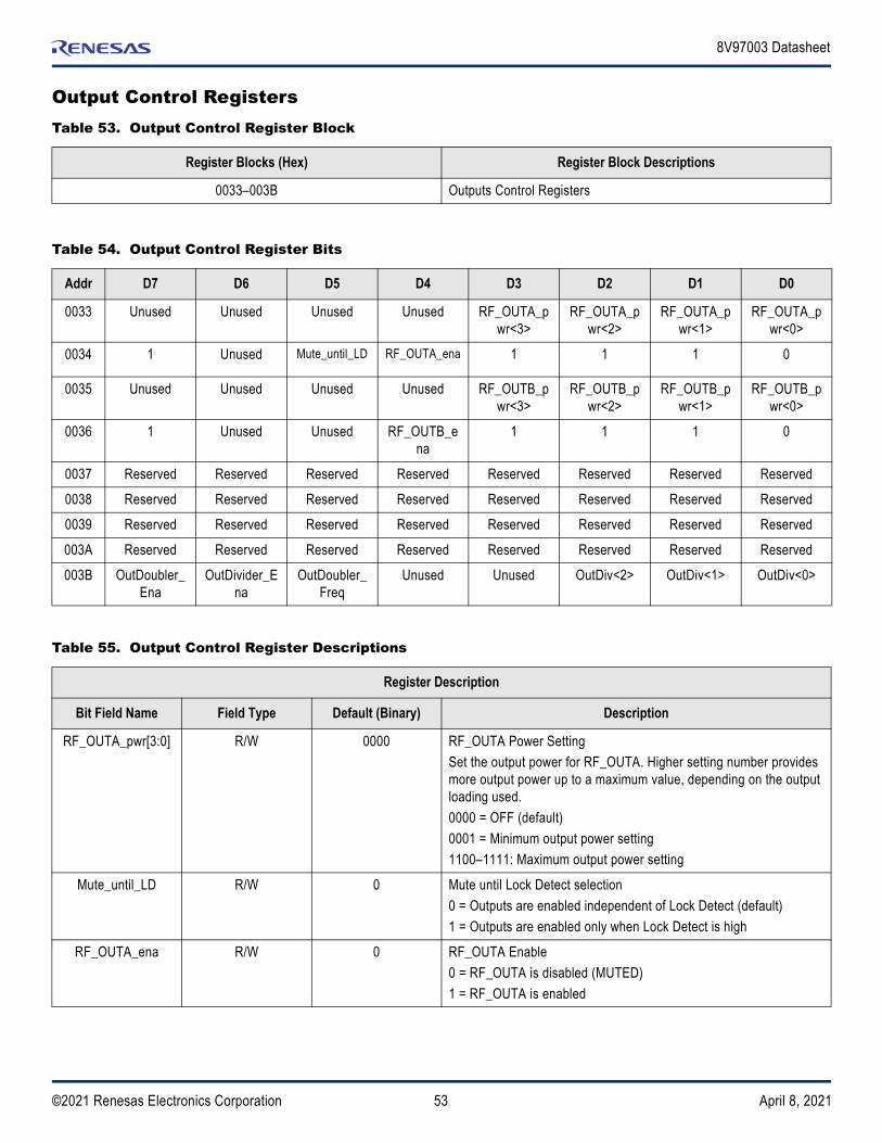
53©2021 Renesas Electronics Corporation April 8, 2021
8V97003 Datasheet
Output Control RegistersTable 53. Output Control Register Block
Register Blocks (Hex) Register Block Descriptions
0033–003B Outputs Control Registers
Table 54. Output Control Register Bits
Addr D7 D6 D5 D4 D3 D2 D1 D0
0033 Unused Unused Unused Unused RF_OUTA_pwr<3>
RF_OUTA_pwr<2>
RF_OUTA_pwr<1>
RF_OUTA_pwr<0>
0034 1 Unused Mute_until_LD RF_OUTA_ena 1 1 1 0
0035 Unused Unused Unused Unused RF_OUTB_pwr<3>
RF_OUTB_pwr<2>
RF_OUTB_pwr<1>
RF_OUTB_pwr<0>
0036 1 Unused Unused RF_OUTB_ena
1 1 1 0
0037 Reserved Reserved Reserved Reserved Reserved Reserved Reserved Reserved
0038 Reserved Reserved Reserved Reserved Reserved Reserved Reserved Reserved
0039 Reserved Reserved Reserved Reserved Reserved Reserved Reserved Reserved
003A Reserved Reserved Reserved Reserved Reserved Reserved Reserved Reserved
003B OutDoubler_Ena
OutDivider_Ena
OutDoubler_Freq
Unused Unused OutDiv<2> OutDiv<1> OutDiv<0>
Table 55. Output Control Register Descriptions
Register Description
Bit Field Name Field Type Default (Binary) Description
RF_OUTA_pwr[3:0] R/W 0000 RF_OUTA Power Setting
Set the output power for RF_OUTA. Higher setting number provides more output power up to a maximum value, depending on the output loading used.
0000 = OFF (default)
0001 = Minimum output power setting
1100–1111: Maximum output power setting
Mute_until_LD R/W 0 Mute until Lock Detect selection
0 = Outputs are enabled independent of Lock Detect (default)
1 = Outputs are enabled only when Lock Detect is high
RF_OUTA_ena R/W 0 RF_OUTA Enable
0 = RF_OUTA is disabled (MUTED)
1 = RF_OUTA is enabled

54©2021 Renesas Electronics Corporation April 8, 2021
8V97003 Datasheet
RF_OUTB_pwr[3:0] R/W 0000 RF_OUTB Power Setting
Set the output power for RF_OUTB. Higher setting number provides more output power up to a maximum value, depending on the output loading used.
0000 = OFF (Default)
0001 = Minimum output power setting
1100–1111: Maximum output power setting
RF_OUTB_ena R/W 0 RF_OUTB Enable
0 = RF_OUTB is disabled (MUTED)
1 = RF_OUTB is enabled
OutDoubler_Ena R/W 0 RF Output Doubler Enable[a]
0 = 1x path (Divide by 1) path Enabled (default)[b]
1 = 2x path Enabled (RF Output Doubler Enabled)
OutDivider_Ena R/W 0 RF Output Divider Enable
0 = 1x or 2x path Enabled (default)
1 = RF Output Divider Enabled
Note: The output divider M0 can only be used (OutDivider_Ena=1) if the output doubler is disabled (OutDoubler_Ena=0).[c]
OutDoubler_Freq R/W 1 RF Output Doubler Frequency Setting
0 = Use this setting for VCO frequency = 7.0-9.0GHz (default)
1 = Use this setting for VCO frequency = 5.5-7.0GHz
OutDiv[2:0] R/W 000 RF Output Divider (M0) Settings
000 = Unused
001 = Div By 2
010 = Div By 4
011 = Div By 8
100 = Div By 16
101 = Div By 32
110 = Unused
111 = Unused
[a] OutDoubler_Ena can only be set to 1 if the VCO frequency is not greater than 9GHz.
[b] For Divide by 1 (Output Divider and Doubler bypassed), both OutDoubler_Ena Bit and Out_Divider_Ena bit must be set 0 (Low).
[c] Both the OutDoubler_Ena and Out_Divider_Ena bits must not be set 1 (High) at the same time.
Table 55. Output Control Register Descriptions (Cont.)
Register Description
Bit Field Name Field Type Default (Binary) Description

55©2021 Renesas Electronics Corporation April 8, 2021
8V97003 Datasheet
Status RegistersTable 56. Status Register Block
Register Blocks (Hex) Register Block Descriptions
0044 Digital Lock and Calibration and VCO Status Registers
0045 Digital Band Status Registers
0046–0047 Reserved
0048 Unused
0049 Loss of Lock Status Registers
Table 57. Status Register Bits
Addr D7 D6 D5 D4 D3 D2 D1 D0
0044 DigLock BandSelDone Unused Unused VcoSts<3> VcoSts<2> VcoSts<1> VcoSts<0>
0045 Unused BandSts<6> BandSts<5> BandSts<4> BandSts<3> BandSts<2> BandSts<1> BandSts<0>
0046 0 0 0 0 0 0 0 0
0047 Unused Unused 0 0 0 0 0 0
0048 Unused Unused Unused Unused Unused Unused Unused Unused
0049 Unused Unused Unused Unused Unused LossLock Unused Unused
Table 58. Status Register Descriptions
Register Description
Bit Field Name Field Type Default (Binary) Description
DigLock R 0 Digital Lock
0 = PLL not locked
1 = PLL locked (according to LDP settings in Register 39)
BandSelDone R 0 Band Select Done (calibration completed)
0 = Band selection not completed
1 = Band selection completed
VcoSts[3:0] R 0000 Status bits reporting the current VCO
0000 = VCO0
0001 = VCO1
…
0111 = VCO7
1000–1111 = Unused
BandSts[6:0] R 000 0000 Status bits reporting the current digital band
000 0000 = Band0
000 0001 = Band1
...
111 1111 = Band127

56©2021 Renesas Electronics Corporation April 8, 2021
8V97003 Datasheet
Applications Information
Loop Filter Calculations
2nd Order Loop Filter This section provides design information for a 2nd order loop filter for the 8V97003. A general 2nd order loop filter is shown in Figure 23. Step-by-step calculations to determine Rz, Cz, and Cp values for a desired loop bandwidth are described below. Required parameters are provided. A spreadsheet for calculating the loop filter values is also available.
Figure 23. Typical 2nd Order Loop Filter
1. Determine desired loop bandwidth fc.
2. Calculate Rz:
Where,
ICP is charge pump current. ICP is programmable from 166µA to 10.66mA.
N is effective feedback divider. N must be programmed into the following value.
fVCO is VCO frequency. VCO frequency range: 5500 to 11000MHz
LossLock R/W1C 0 Status bit stating device loss of lock
Sticky bit. Write 1 to this bit to clear
0 = Locked since last time register was cleared
1 = Loss of Lock since last time register was cleared
Table 58. Status Register Descriptions (Cont.)
Register Description
Bit Field Name Field Type Default (Binary) Description
RZ
CZ
Cp
RZ2 fc NICP KVCO----------------------------------=
NfVCOfPFD----------------=

57©2021 Renesas Electronics Corporation April 8, 2021
8V97003 Datasheet
fPFD is phase detector input frequency.
fREF is reference clock (REF_IN) input frequency.
PV is overall pre-divider or input doubler setting.
KVCO is VCO gain depends on VCO Frequency (see VCO gain in KVCO in Table 11).
3. Calculate Cz:
Where,
= fc/ fz, user can determine an number.
> 6 is recommended.
fz is frequency at zero.
4. Calculate Cp:
Where,
= fp/fc, user can determine number.
> 4 is recommended.
fp is frequency at pole.
5. Verify Phase Margin (PM).
Where,
The phase margin (PM) should be greater than 50°.
A spreadsheet for calculating the loop filter component values is available at www.IDT.com. To use the spreadsheet, simply enter the following parameters:
fc, F_ref, PV, Icp, FVCO, and .
The spreadsheet will provide the component values, Rz, Cz, and Cp as the result. The spreadsheet also calculates the maximum phase margin for verification.
fPFDfREF
PV-------------=
CZ
2 fc RZ--------------------------------------=
CP
CZ -------------=
PM arb 1–
2 b---------------- tan=
Cp
Czb 1

58©2021 Renesas Electronics Corporation April 8, 2021
8V97003 Datasheet
3rd Order Loop FilterThis section provides design information for a 3rd order loop filter for the 8V97003. A general 3rd order loop filter is shown in Figure 24.
Figure 24. Typical 3rd Order Loop Filter
The Rz, Cz, and Cp can be calculated as 2nd order loop filter. The following equation helps determine the 3rd order loop filter Rp2 and Cp2.
Pick an Rp2 value. Rp2 ~ 1.5xRz is suggested.
Where,
is ratio between the 1st pole frequency and the 2nd pole frequency.
> 4 is recommended.
Figure 25 shows an example of a loop filter that can be used on the 8V97003.
Figure 25. Loop Filter Example
Rz
Cz
Cp
Rp2
Cp2
RP2
CP2CP
RZ
CZ

59©2021 Renesas Electronics Corporation April 8, 2021
8V97003 Datasheet
Recommendations for Unused Input and Output Pins
Inputs
LVCMOS Control Pins
All control pins have internal pullup and pulldown resistors; additional resistance is not required but can be added for additional protection. A 1k resistor can be used.
Outputs
Output Pins
For any unused output, it can be left floating and disabled.
Schematic ExampleFigure 26 shows a general application schematic example for the 8V97003.
For power rails, bypass capacitors must be provided to all power supply pins. At least one bypass capacitor per power pin is suggested. Value can range from 0.01µF or 0.1µF. Mix values of bypass capacitors can help filtering wider range of power supply noise.
The 8V97003 input is high impedance. The input termination depends on the termination requirement from the driver. There are two input termination examples in the schematic shown in Figure 26; both are designed for transmission line with characteristic impedance Zo = 50Ω.
The first example, labeled “Input Reference” at the lower right corner of the schematic, shows an input termination scheme for accepting a reference clock from bench signal generators. 50Ω resistors, R82 and R83 to GND, present matched loads to signal generator’s source impedance; the reference clock signal is then AC-coupled with capacitors C156 and C157 to ensure proper DC-biased to level of VDDx/2 by voltage divider networks of R90, R91, R92, and R93. The second example shows an input termination scheme for accepting a reference clock from a TCXO. The values of R96, R96, R85, and R88 in this example are designed for a TCXO with a single-ended CMOS output on pin 5. They can be changed for different TCXO output signal types.
The 8V97003 output pull-up loading can be resistors or inductors. For inductor pull-up loading, the inductor value is frequency dependent. One inductor value cannot cover all the output frequency range. For example, an inductance of L = 1.3nH that is suitable for approximately 6GHz operating frequency. The output can also drive single ended LO input.
Figure 26 also shows an example of the 8V97003 output driving single-ended LO input of the mixer through an LC balun. The LC balun component values are frequency dependent. These values can be adjusted to optimize the performance. A single-ended LO receiver input also can tap to one side of the differential driver using resistor loading or inductor loading. For single-ended LO input, both sides of the differential driver still need to be loaded with a pull up. The output power level can also be adjusted further through programming.
The loop filter values can be calculated to meet the loop bandwidth requirement (for detailed calculations, see Loop Filter Calculations).

60©2021 Renesas Electronics Corporation April 8, 2021
8V97003 Datasheet
Figure 26. Schematic Example
Power ConsiderationsThis section provides information on power dissipation and junction temperature for the 8V97003. Equations and example calculations are also provided.
1. Power Dissipation.
The power dissipation for the 8V97003 is the total power minus the power dissipated into the loads. The following is the power dissipation for VDDx = 3.3V + 5% = 3.465V at ambient temperature of 95°C.
Maximum current at 95°C, IDDx_MAX = 650mA (see Table 8)
Total Power Dissipation: Power_MAX = VDDx_MAX * IDDx_MAX = 3.465V * 650mA = 2252mW
Power dissipation in external loads for both outputs: Power (output)MAX = 2 * ILOAD2 * 50Ω = 22.5mW (Load Current with Out_Pwr = 0101, ILOAD = 15mA)
Power Dissipation, PD = Power_MAX – Power (output)MAX = 2252mA - 22.5mW = 2229.5mW
5
5
4
4
3
3
2
2
1
1
4 4
3 3
2 2
1 1
nREFIN
Placed decoupling capacitors close to power pins
REFIN
Place output traces on top layer. Make them as short as possible
TOP LAYER 1oz COPPER
BOTTOM LAYER 1oz COPPER
GROUND PLANE
POWER PLANE
Board Layer Stack-up (62mil)
nRESET
TCXO Layout Notes:
1. Overlapping U5 and U7 footprint2. U7 uses 4 pads; U5 can use 6pads (skipping 4 and 8)
3. Keeping branching traces short
DNI
DNI
DNI
DNI
4. R46/47 are DNIs unless U5 orU7 is used
6. Place R46/R47 close to thebranching point merging with SMAtraces of the same net names.
5. R44/45 and R48/49 are usedonly when U7 is used DNI
DNI
VDD_DIG
GND_D
GND_DGND_D
VDDOUTA
VDDVCOVDDOUTAVDDOUTB VDD_DIG VDD_INPDFB
GND_D GND_DGND_DGND_DGND_D
GND_D
GND_D
VDD_DIG
GND_D
GND_D
VDDOUTB
GND_D
GND_D GND_D
GND_D
GND_D
GND_D
VDDTCXO
GND_D
VDDTCXO
GND_D
VDDTCXO
VDD_INPDFB
VDD_INPDFB
GND_D
GND_D
GND_D
GND_D
GND_D
GND_D
SPI_CSN 3SPI_CLK 3
SPI_DIO 3SPI_SDO
Title
Size Document Number Rev
Date: Sheet of
<Doc> <RevCode>
<Title>
C
1 3Thursday, March 26, 2020
Title
Size Document Number Rev
Date: Sheet of
<Doc> <RevCode>
<Title>
C
1 3Thursday, March 26, 2020
Title
Size Document Number Rev
Date: Sheet of
<Doc> <RevCode>
<Title>
C
1 3Thursday, March 26, 2020
R16100
R53
1K
C9
0.1u
U5
RHF7050
NC11
E_D2
GND3
OUT5
nOUT6
VDD7
R350
21
C8
0.1u
C92 0.01u
J3
S1
G2
G3
G4
G5
R250
21
R7 1K C20
680pF
C2
0.1u
J1
S1
G2
G3
G4
G5
R6
360
U1
8V9700
VDDVCO133
VDDVCO23
VDDPDCP12
VDDFB15
VDDIN24
VDDDIG18
VDDOUTA37
VDDOUTB48
VSSPDCP14
VSSFB17
VSSDIG19
VSSIN20
VSSOUTA138
VSSOUTA241
VSSOUTB144
VSSOUTB247
EPAD49
RF_OUTA40
nRF_OUTA39
RF_OUTB45
nRF_OUTB46
CPOUT10
VTUNE5
NC9
CSB25
SCLK26
SDO27
SDIO28
CE29MUTE7LD8
VREGVCO132
NC34
VREFVCO135
NC36
VREFVCO21
NC2
VREGVCO24
CPBIAS11
NC13
NC16
NC21
NC42
NC43
SYNC30
NC6
REF_IN22
nREF_IN23
RESET31
C12
0.01u
R45
1K
R50
1K
R8
2.2K
J5 TP
R450
21
C10
0.1u
R10
50
C2147nF
C17
22u
R13
2.2K
C24
22u
C26
22u
R44
1K
J2
S1
G2
G3
G4
G5
R51
1K
C1 0.1u
U7
RPT5032N
NC1
GND2
OUT3
VCC4
C13 0.1u
C33 0.1u
C91 0.01u
R9
2.2K
R48100
J8S1
G2
G3
G4
G5
C4
0.1u
R12
2.2K
C7
0.1u
C5 0.1u
J4
S1
G2
G3
G4
G5
C32 0.1u
R47 0
C19
2.7nF
C14 0.1u
R52
1K
J6S1
G2
G3
G4
G5
C6
0.1uL3 18nH
11
22
J16
S1
G2
G3
G4
G5
R49100
SW1 A1
B2 B1
A2
C15
22u
R5 1K
C3
0.1u
R15
50
LD1
R1
50
21
L2 18nH
11
22
C11
0.01u
C22
22u
R46 0
nREFIN
REFIN
RF_OUTA
nRF_OUTA
RF_OUTB
nRF_OUTB
SPI_CSNSPI_CLK
SPI_DIO
nRESET
REFIN
nREFIN

61©2021 Renesas Electronics Corporation April 8, 2021
8V97003 Datasheet
2. Junction Temperature.
Junction temperature, Tj, signifies the hottest point on the device and exceeding the specified limit could cause device reliability issues. The maximum recommended junction temperature is 125°C.
For devices like this and in systems where most heat escapes from the bottom exposed pad of the package, θJB is the primary thermal resistance of interest.
The equation to calculate Tj using θJB is: Tj = θJB * PD + TB:
Tj = Junction Temperature
θJB = Junction-to-Board Thermal Resistance
PD = Device Power Dissipation (example calculation is in section 1 above)
TB = Board Temperature
In order to calculate junction temperature, the appropriate junction-to-board thermal resistance θJB must be used. Assuming a 2-ground plane board, the appropriate value of θJB is 0.76°C/W (see Table 6).
Therefore, Tj for a PCB maintained at 105°C with the outputs switching is:
105°C + 2.2295W * 0.76°C/W = 106.5°C which is below the limit of 125°C.
This calculation is only an example. Tj will obviously vary depending on the number of loaded outputs, supply voltage, air flow, heat transfer method, the type of board (multi-layer) and the actual maintained board temperature.
Package Outline DrawingsThe package outline drawings are appended at the end of this document and are accessible from the link below. The package information is the most current data available.
www.idt.com/document/psc/48-vfqfpn-package-outline-drawing-70-x70-x-085-mm-body-05mm-pitch-epad-530-x-530-mm-nlg48p3
Marking Diagram
Lines 1–3 indicate the part number.
Line 4 indicates the following:
• “#” denotes stepping.
• “YY” is the last two digits of the year; “WW” is the work week number when the part was assembled.
• “$” denotes the mark code.

62©2021 Renesas Electronics Corporation April 8, 2021
8V97003 Datasheet
Ordering InformationTable 59. Ordering Information
Orderable Part Number Package Shipping Packaging Temperature
8V97003NLGI 7 7 mm 48-VFQFPN, Lead-free Tray -40°C to +95°C
8V97003NLGI87 7 mm 48-VFQFPN, Lead-freePin 1 Orientation: Quadrant 1 (EIA-481-C)
Tape and Reel -40°C to +95°C
8V97003NLGI/W7 7 mm 48-VFQFPN, Lead-freePin 1 Orientation: Quadrant 2 (EIA-481-D)
Tape and Reel -40°C to +95°C
Table 60. Pin 1 Orientation in Tape and Reel Packaging
Part Number Suffix Pin 1 Orientation Illustration
NLGI8 Quadrant 1 (EIA-481-C)
NLGI/W Quadrant 2 (EIA-481-D)

63©2021 Renesas Electronics Corporation April 8, 2021
8V97003 Datasheet
Revision History
Revision Date Description of Change
April 8, 2021 Added Figure 9
November 17, 2020 Changed the pull-up/pull-down status of pin 31 (nRESET) to PU in Pin Descriptions Updated Figure 25 Added a note to Reference Multiplier (MULT)
September 15, 2020
Updated the phase adjustment formulas and the last sentence in Phase Adjust Updated the description of Output Phase Synchronization Updated the first line of each field description in Table 25 Updated the description of ManualReSync in Table 34 Updated the description of AutoReSync in Table 52
April 7, 2020
Updated the description of CE in Table 1 Updated the Power-Down Current parameter in Table 8 Updated Reference Input Stage Changed D7 in register 0x0028 to reserved. Also updated the description of VCO_En in the same register
(see Power Down Control Registers) Updated the schematic example in Figure 26 Updated loop filter values and typo corrections
January 20, 2020 Corrected a typo for the maximum power setting in the typical current in Table 9 Added a description for register 7 (Chip option) (see Table 16 and Table 22)
January 8, 2020
Corrected the product description on page 1 to indicate output frequency support of “171.875MHz to 18GHz”
Updated the fRF_OUT = 8GHz test condition for tjit(Ø) in Table 12 Updated Figure 4 Rebranded the document as Renesas
December 20, 2019 Initial release.

© Integrated Device Technology, Inc.
48-VFQFPN, Package Outline Drawing
7.0 x7.0 x 0.85 mm Body, 0.5mm Pitch, Epad 5.30 x 5.30 mmNLG48P3, PSC-4203-04, Rev 02, Page 1
AutoCAD SHX Text
INDEX AREA
AutoCAD SHX Text
NOTES: 1. ALL DIMENSIONING AND TOLERANCING CONFORM TO ANSI Y14.5M-1982 2 ALL DIMENSIONS ARE IN MILLIMETERS. 3. INDEX AREA (PIN1 IDENTIFIER)
AutoCAD SHX Text
SEATING PLANE
AutoCAD SHX Text
0.00
AutoCAD SHX Text
TOP VIEW
AutoCAD SHX Text
SIDE VIEW
AutoCAD SHX Text
BOTTOM VIEW
AutoCAD SHX Text
Pin1 ID
AutoCAD SHX Text
C0.35
AutoCAD SHX Text
48x
AutoCAD SHX Text
0.30
AutoCAD SHX Text
0.20
AutoCAD SHX Text
0.45
AutoCAD SHX Text
0.35
AutoCAD SHX Text
48x
AutoCAD SHX Text
1
AutoCAD SHX Text
12
AutoCAD SHX Text
13
AutoCAD SHX Text
24
AutoCAD SHX Text
25
AutoCAD SHX Text
36
AutoCAD SHX Text
37
AutoCAD SHX Text
48

© Integrated Device Technology, Inc.
48-VFQFPN, Package Outline Drawing
7.0 x7.0 x 0.85 mm Body, 0.5mm Pitch, Epad 5.30 x 5.30 mmNLG48P3, PSC-4203-04, Rev 02, Page 2
Package Revision HistoryRev No.Date Created Description
July 24, 2018 Rev 02 Change P4 to P3
July 9, 2018 Rev 01 New Format, Change QFN to VFQFPN
AutoCAD SHX Text
RECOMMENDED LAND PATTERN DIMENSION
AutoCAD SHX Text
1. ALL DIMENSIONS ARE IN MM. ANGLES IN DEGREES.
AutoCAD SHX Text
2. TOP DOWN VIEW. AS VIEWED ON PCB.
AutoCAD SHX Text
3. LAND PATTERN IN BLUE. NSMD PATTERN ASSUMED.
AutoCAD SHX Text
4. LAND PATTERN RECOMMENDATION PER IPC-7351B GENERIC REQUIREMENT
AutoCAD SHX Text
NOTES:
AutoCAD SHX Text
FOR SURFACE MOUNT DESIGN AND LAND PATTERN.
AutoCAD SHX Text
C0.35
Corporate HeadquartersTOYOSU FORESIA, 3-2-24 Toyosu,Koto-ku, Tokyo 135-0061, Japanwww.renesas.com
Contact InformationFor further information on a product, technology, the most up-to-date version of a document, or your nearest sales office, please visit:www.renesas.com/contact/
TrademarksRenesas and the Renesas logo are trademarks of Renesas Electronics Corporation. All trademarks and registered trademarks are the property of their respective owners.
IMPORTANT NOTICE AND DISCLAIMER
RENESAS ELECTRONICS CORPORATION AND ITS SUBSIDIARIES (“RENESAS”) PROVIDES TECHNICAL SPECIFICATIONS AND RELIABILITY DATA (INCLUDING DATASHEETS), DESIGN RESOURCES (INCLUDING REFERENCE DESIGNS), APPLICATION OR OTHER DESIGN ADVICE, WEB TOOLS, SAFETY INFORMATION, AND OTHER RESOURCES “AS IS” AND WITH ALL FAULTS, AND DISCLAIMS ALL WARRANTIES, EXPRESS OR IMPLIED, INCLUDING, WITHOUT LIMITATION, ANY IMPLIED WARRANTIES OF MERCHANTABILITY, FITNESS FOR A PARTICULAR PURPOSE, OR NON-INFRINGEMENT OF THIRD PARTY INTELLECTUAL PROPERTY RIGHTS.
These resources are intended for developers skilled in the art designing with Renesas products. You are solely responsible for (1) selecting the appropriate products for your application, (2) designing, validating, and testing your application, and (3) ensuring your application meets applicable standards, and any other safety, security, or other requirements. These resources are subject to change without notice. Renesas grants you permission to use these resources only for development of an application that uses Renesas products. Other reproduction or use of these resources is strictly prohibited. No license is granted to any other Renesas intellectual property or to any third party intellectual property. Renesas disclaims responsibility for, and you will fully indemnify Renesas and its representatives against, any claims, damages, costs, losses, or liabilities arising out of your use of these resources. Renesas' products are provided only subject to Renesas' Terms and Conditions of Sale or other applicable terms agreed to in writing. No use of any Renesas resources expands or otherwise alters any applicable warranties or warranty disclaimers for these products.
(Rev.1.0 Mar 2020)
© 2020 Renesas Electronics Corporation. All rights reserved.