Silicon photonics integrated design - UGentphotonics.intec.ugent.be/download/pub_3130.pdf ·...
4
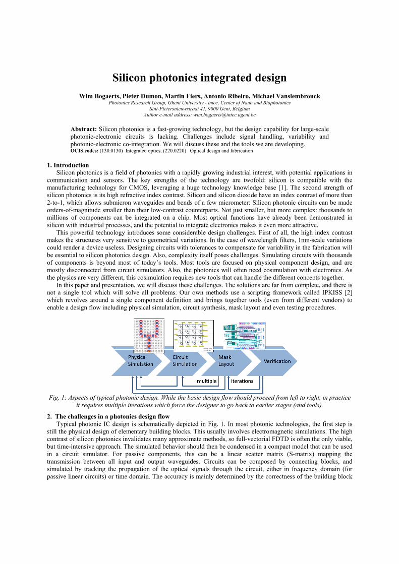
Silicon photonics integrated design Wim Bogaerts, Pieter Dumon, Martin Fiers, Antonio Ribeiro, Michael Vanslembrouck Photonics Research Group, Ghent University - imec, Center of Nano and Biophotonics Sint-Pietersnieuwstraat 41, 9000 Gent, Belgium Author e-mail address: [email protected] Abstract: Silicon photonics is a fast-growing technology, but the design capability for large-scale photonic-electronic circuits is lacking. Challenges include signal handling, variability and photonic-electronic co-integration. We will discuss these and the tools we are developing. OCIS codes: (130.0130) Integrated optics, (220.0220) Optical design and fabrication 1. Introduction Silicon photonics is a field of photonics with a rapidly growing industrial interest, with potential applications in communication and sensors. The key strengths of the technology are twofold: silicon is compatible with the manufacturing technology for CMOS, leveraging a huge technology knowledge base [1]. The second strength of silicon photonics is its high refractive index contrast. Silicon and silicon dioxide have an index contrast of more than 2-to-1, which allows submicron waveguides and bends of a few micrometer: Silicon photonic circuits can be made orders-of-magnitude smaller than their low-contrast counterparts. Not just smaller, but more complex: thousands to millions of components can be integrated on a chip. Most optical functions have already been demonstrated in silicon with industrial processes, and the potential to integrate electronics makes it even more attractive. This powerful technology introduces some considerable design challenges. First of all, the high index contrast makes the structures very sensitive to geometrical variations. In the case of wavelength filters, 1nm-scale variations could render a device useless. Designing circuits with tolerances to compensate for variability in the fabrication will be essential to silicon photonics design. Also, complexity itself poses challenges. Simulating circuits with thousands of components is beyond most of today’s tools. Most tools are focused on physical component design, and are mostly disconnected from circuit simulators. Also, the photonics will often need cosimulation with electronics. As the physics are very different, this cosimulation requires new tools that can handle the different concepts together. In this paper and presentation, we will discuss these challenges. The solutions are far from complete, and there is not a single tool which will solve all problems. Our own methods use a scripting framework called IPKISS [2] which revolves around a single component definition and brings together tools (even from different vendors) to enable a design flow including physical simulation, circuit synthesis, mask layout and even testing procedures. Fig. 1: Aspects of typical photonic design. While the basic design flow should proceed from left to right, in practice it requires multiple iterations which force the designer to go back to earlier stages (and tools). 2. The challenges in a photonics design flow Typical photonic IC design is schematically depicted in Fig. 1. In most photonic technologies, the first step is still the physical design of elementary building blocks. This usually involves electromagnetic simulations. The high contrast of silicon photonics invalidates many approximate methods, so full-vectorial FDTD is often the only viable, but time-intensive approach. The simulated behavior should then be condensed in a compact model that can be used in a circuit simulator. For passive components, this can be a linear scatter matrix (S-matrix) mapping the transmission between all input and output waveguides. Circuits can be composed by connecting blocks, and simulated by tracking the propagation of the optical signals through the circuit, either in frequency domain (for passive linear circuits) or time domain. The accuracy is mainly determined by the correctness of the building block
Transcript of Silicon photonics integrated design - UGentphotonics.intec.ugent.be/download/pub_3130.pdf ·...
Silicon photonics integrated design
Wim Bogaerts, Pieter Dumon, Martin Fiers, Antonio Ribeiro, Michael Vanslembrouck Photonics Research Group, Ghent University - imec, Center of Nano and Biophotonics
Sint-Pietersnieuwstraat 41, 9000 Gent, Belgium Author e-mail address: [email protected]
Abstract: Silicon photonics is a fast-growing technology, but the design capability for large-scale photonic-electronic circuits is lacking. Challenges include signal handling, variability and photonic-electronic co-integration. We will discuss these and the tools we are developing. OCIS codes: (130.0130) Integrated optics, (220.0220) Optical design and fabrication
1. Introduction
Silicon photonics is a field of photonics with a rapidly growing industrial interest, with potential applications in communication and sensors. The key strengths of the technology are twofold: silicon is compatible with the manufacturing technology for CMOS, leveraging a huge technology knowledge base [1]. The second strength of silicon photonics is its high refractive index contrast. Silicon and silicon dioxide have an index contrast of more than 2-to-1, which allows submicron waveguides and bends of a few micrometer: Silicon photonic circuits can be made orders-of-magnitude smaller than their low-contrast counterparts. Not just smaller, but more complex: thousands to millions of components can be integrated on a chip. Most optical functions have already been demonstrated in silicon with industrial processes, and the potential to integrate electronics makes it even more attractive.
This powerful technology introduces some considerable design challenges. First of all, the high index contrast makes the structures very sensitive to geometrical variations. In the case of wavelength filters, 1nm-scale variations could render a device useless. Designing circuits with tolerances to compensate for variability in the fabrication will be essential to silicon photonics design. Also, complexity itself poses challenges. Simulating circuits with thousands of components is beyond most of today’s tools. Most tools are focused on physical component design, and are mostly disconnected from circuit simulators. Also, the photonics will often need cosimulation with electronics. As the physics are very different, this cosimulation requires new tools that can handle the different concepts together.
In this paper and presentation, we will discuss these challenges. The solutions are far from complete, and there is not a single tool which will solve all problems. Our own methods use a scripting framework called IPKISS [2] which revolves around a single component definition and brings together tools (even from different vendors) to enable a design flow including physical simulation, circuit synthesis, mask layout and even testing procedures.
Fig. 1: Aspects of typical photonic design. While the basic design flow should proceed from left to right, in practice
it requires multiple iterations which force the designer to go back to earlier stages (and tools).
2. The challenges in a photonics design flow Typical photonic IC design is schematically depicted in Fig. 1. In most photonic technologies, the first step is
still the physical design of elementary building blocks. This usually involves electromagnetic simulations. The high contrast of silicon photonics invalidates many approximate methods, so full-vectorial FDTD is often the only viable, but time-intensive approach. The simulated behavior should then be condensed in a compact model that can be used in a circuit simulator. For passive components, this can be a linear scatter matrix (S-matrix) mapping the transmission between all input and output waveguides. Circuits can be composed by connecting blocks, and simulated by tracking the propagation of the optical signals through the circuit, either in frequency domain (for passive linear circuits) or time domain. The accuracy is mainly determined by the correctness of the building block
models and the handling of the optical signals between the blocks. Especially the latter aspect is difficult in cosimulation of photonics and electronics, as signal handling is very different for these two domains.
From the circuit a chip layout should be generated. While in electronics powerful place-and-route tools can automate this process, photonics make this somewhat more complicated. Typical PICs have only a single waveguide layer, and waveguides need to respect conditions such as bend radius, spacing. On the other hand, photonic waveguides can allow some crossings, but traditional electronics P&R tools are not equipped to handle this.
While each step in the design flow poses its challenges, the flow as a whole is also not well supported. Different steps require different tools, and data exchange between tools is poorly automated. In practice, designers redefine components in each tool. If you consider that the design flow will not be linear, and that the designer often has to take a step back, errors or inconsistencies will quickly propagate into the layout. Of course, the layout should be verified before fabrication. Here, photonics is still at the first stage. Powerful tools exist that analyze electronic layouts to and compare it to the original circuit design, but such tools have yet to be developed for photonic integrated circuits: Interconnectivity in photonics is very different than in electronics, with the possibility of crossing waveguides or evanescent coupling. Also, waveguides can transport many wavelength channels, and in different directions. Efficient and accurate layout-versus-schematic (LVS) for photonics is therefore not yet a reality.
And where in this flow is variability introduced? In the physical design phase, or in the circuit design? Bringing in statistics from the fabrication needs to go beyond the traditional corner analysis describing the fast and slow corners of a pmos and nmos transistor: variability can be statistically random but might also be location-dependent.
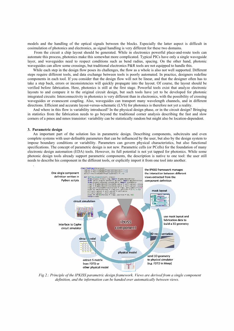
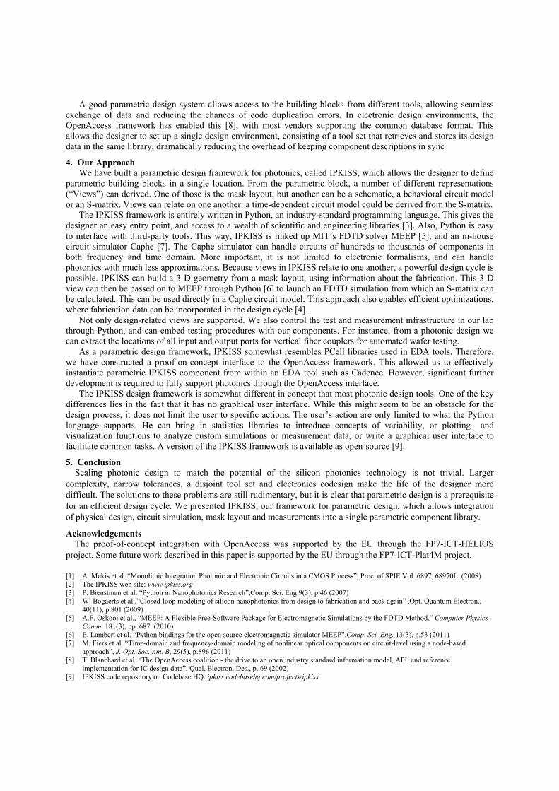
3. Parametric design An important part of the solution lies in parametric design. Describing components, subcircuits and even
complete systems with user-definable parameters that can be influenced by the user, but also by the design system to impose boundary conditions or variability. Parameters can govern physical characteristics, but also functional specifications. The concept of parametric design is not new. Parametric cells (or PCells) for the foundation of many electronic design automation (EDA) tools. However, its full potential is not yet tapped for photonics. While some photonic design tools already support parametric components, the description is native to one tool: the user still needs to describe his component in the different tools, or explicitly import it from one tool into another.
.
Fig 2.: Principle of the IPKISS parametric design framework. Views are derived from a single component
definition, and the information can be handed over automatically between views.
A good parametric design system allows access to the building blocks from different tools, allowing seamless exchange of data and reducing the chances of code duplication errors. In electronic design environments, the OpenAccess framework has enabled this [8], with most vendors supporting the common database format. This allows the designer to set up a single design environment, consisting of a tool set that retrieves and stores its design data in the same library, dramatically reducing the overhead of keeping component descriptions in sync
4. Our Approach We have built a parametric design framework for photonics, called IPKISS, which allows the designer to define
parametric building blocks in a single location. From the parametric block, a number of different representations (“Views”) can derived. One of those is the mask layout, but another can be a schematic, a behavioral circuit model or an S-matrix. Views can relate on one another: a time-dependent circuit model could be derived from the S-matrix.
The IPKISS framework is entirely written in Python, an industry-standard programming language. This gives the designer an easy entry point, and access to a wealth of scientific and engineering libraries [3]. Also, Python is easy to interface with third-party tools. This way, IPKISS is linked up MIT’s FDTD solver MEEP [5], and an in-house circuit simulator Caphe [7]. The Caphe simulator can handle circuits of hundreds to thousands of components in both frequency and time domain. More important, it is not limited to electronic formalisms, and can handle photonics with much less approximations. Because views in IPKISS relate to one another, a powerful design cycle is possible. IPKISS can build a 3-D geometry from a mask layout, using information about the fabrication. This 3-D view can then be passed on to MEEP through Python [6] to launch an FDTD simulation from which an S-matrix can be calculated. This can be used directly in a Caphe circuit model. This approach also enables efficient optimizations, where fabrication data can be incorporated in the design cycle [4].
Not only design-related views are supported. We also control the test and measurement infrastructure in our lab through Python, and can embed testing procedures with our components. For instance, from a photonic design we can extract the locations of all input and output ports for vertical fiber couplers for automated wafer testing.
As a parametric design framework, IPKISS somewhat resembles PCell libraries used in EDA tools. Therefore, we have constructed a proof-on-concept interface to the OpenAccess framework. This allowed us to effectively instantiate parametric IPKISS component from within an EDA tool such as Cadence. However, significant further development is required to fully support photonics through the OpenAccess interface.
The IPKISS design framework is somewhat different in concept that most photonic design tools. One of the key differences lies in the fact that it has no graphical user interface. While this might seem to be an obstacle for the design process, it does not limit the user to specific actions. The user’s action are only limited to what the Python language supports. He can bring in statistics libraries to introduce concepts of variability, or plotting and visualization functions to analyze custom simulations or measurement data, or write a graphical user interface to facilitate common tasks. A version of the IPKISS framework is available as open-source [9].
5. Conclusion Scaling photonic design to match the potential of the silicon photonics technology is not trivial. Larger
complexity, narrow tolerances, a disjoint tool set and electronics codesign make the life of the designer more difficult. The solutions to these problems are still rudimentary, but it is clear that parametric design is a prerequisite for an efficient design cycle. We presented IPKISS, our framework for parametric design, which allows integration of physical design, circuit simulation, mask layout and measurements into a single parametric component library.
Acknowledgements The proof-of-concept integration with OpenAccess was supported by the EU through the FP7-ICT-HELIOS
project. Some future work described in this paper is supported by the EU through the FP7-ICT-Plat4M project.
[1] A. Mekis et al. “Monolithic Integration Photonic and Electronic Circuits in a CMOS Process”, Proc. of SPIE Vol. 6897, 68970L, (2008) [2] The IPKISS web site: www.ipkiss.org [3] P. Bienstman et al. “Python in Nanophotonics Research”,Comp. Sci. Eng 9(3), p.46 (2007) [4] W. Bogaerts et al.,”Closed-loop modeling of silicon nanophotonics from design to fabrication and back again” ,Opt. Quantum Electron.,
40(11), p.801 (2009) [5] A.F. Oskooi et al., “MEEP: A Flexible Free-Software Package for Electromagnetic Simulations by the FDTD Method,” Computer Physics
Comm. 181(3), pp. 687. (2010) [6] E. Lambert et al. “Python bindings for the open source electromagnetic simulator MEEP”,Comp. Sci. Eng. 13(3), p.53 (2011) [7] M. Fiers et al. “Time-domain and frequency-domain modeling of nonlinear optical components on circuit-level using a node-based
approach”, J. Opt. Soc. Am. B, 29(5), p.896 (2011) [8] T. Blanchard et al. “The OpenAccess coalition - the drive to an open industry standard information model, API, and reference
implementation for IC design data”, Qual. Electron. Des., p. 69 (2002) [9] IPKISS code repository on Codebase HQ: ipkiss.codebasehq.com/projects/ipkiss