Silicon Laser Shyam Sabanathan Chenjing Li Thannirmalai.
15
Silicon Laser Shyam Sabanathan Chenjing Li Thannirmalai
-
date post
20-Dec-2015 -
Category
Documents
-
view
215 -
download
0
Transcript of Silicon Laser Shyam Sabanathan Chenjing Li Thannirmalai.
Silicon LaserSilicon Laser
Shyam Sabanathan Chenjing Li
Thannirmalai
Shyam Sabanathan Chenjing Li
Thannirmalai
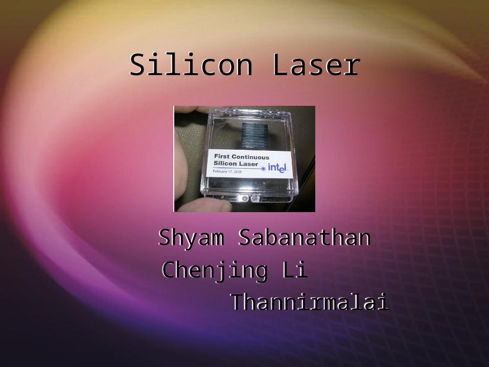
Silicon and its propertiesSilicon and its properties
• It is semiconductor which is used in most of the electronic devices. It is found abundant in nature.
• The silicon atom gas the following electronic configuration [Ne].3s2.3p2. It has four electrons in its valence shell. They are insulators in pure state.
• It is semiconductor which is used in most of the electronic devices. It is found abundant in nature.
• The silicon atom gas the following electronic configuration [Ne].3s2.3p2. It has four electrons in its valence shell. They are insulators in pure state.

• It can be converted to a conductor by doping.
• N-type doping: phosphorus or arsenic is added to the silicon in small quantities. Phosphorus and arsenic each have five outer electrons. The fifth electron has nothing to bond to, so it's free to move around. N-type silicon is a good conductor. Electrons have a negative charge, hence the name N-type.
• P-type doping: doping, boron or gallium is the dopant. Boron and gallium each have only three outer electrons. They form "holes" in the silicon lattice where a silicon electron has nothing to bond to. The absence of an electron creates the effect of a positive charge, hence the name P-type. P-type silicon is a good conductor.

Concentration of the dopant vs Resistivity inSilicon
Concentration of the dopant vs Resistivity inSilicon
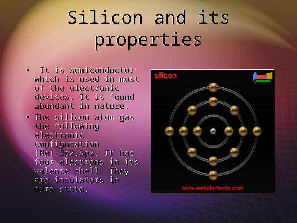
Introduction to LasersIntroduction to Lasers Light Amplification by
Simulated Emission of Radiation
Laser light is monochromatic, coherent, and moves in the same direction
In 1916, Albert Einstein, laid the foundation for the invention of the laser and its predecessor, the maser, in a ground-breaking rederivation of Max Planck's law of radiation based on the concepts of probability coefficients for the absorption, spontaneous and stimulated emission.
Light Amplification by Simulated Emission of Radiation
Laser light is monochromatic, coherent, and moves in the same direction
In 1916, Albert Einstein, laid the foundation for the invention of the laser and its predecessor, the maser, in a ground-breaking rederivation of Max Planck's law of radiation based on the concepts of probability coefficients for the absorption, spontaneous and stimulated emission.

Silicon LaserSilicon Laser
Raman LaserHybrid Silicon Laser
Raman LaserHybrid Silicon Laser
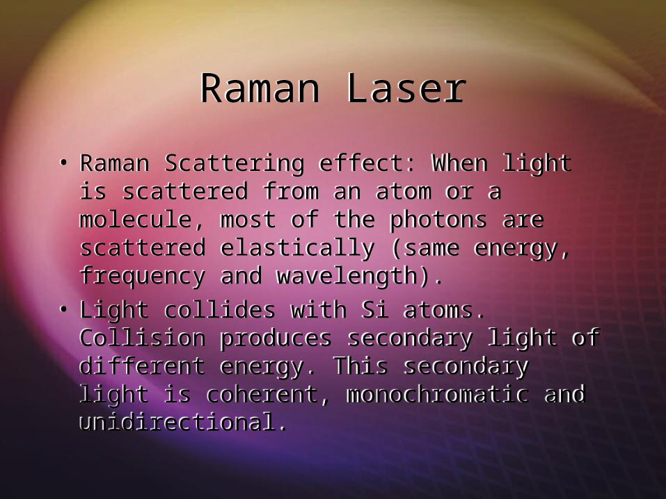
Raman LaserRaman Laser
• Raman Scattering effect: When light is scattered from an atom or a molecule, most of the photons are scattered elastically (same energy, frequency and wavelength).
• Light collides with Si atoms. Collision produces secondary light of different energy. This secondary light is coherent, monochromatic and unidirectional.
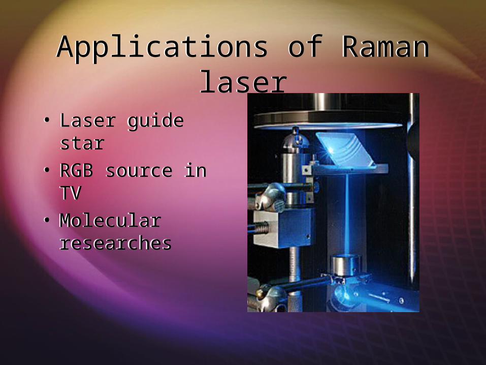
Applications of Raman laser
Applications of Raman laser
• Laser guide star• RGB source in TV• Molecular
researches
• Laser guide star• RGB source in TV• Molecular
researches
Hybrid Silicon Laser Demonstration
Hybrid Silicon Laser Demonstration
http://www.youtube.com/watch?v=f0XTK_a4v9c
http://www.youtube.com/watch?v=f0XTK_a4v9c
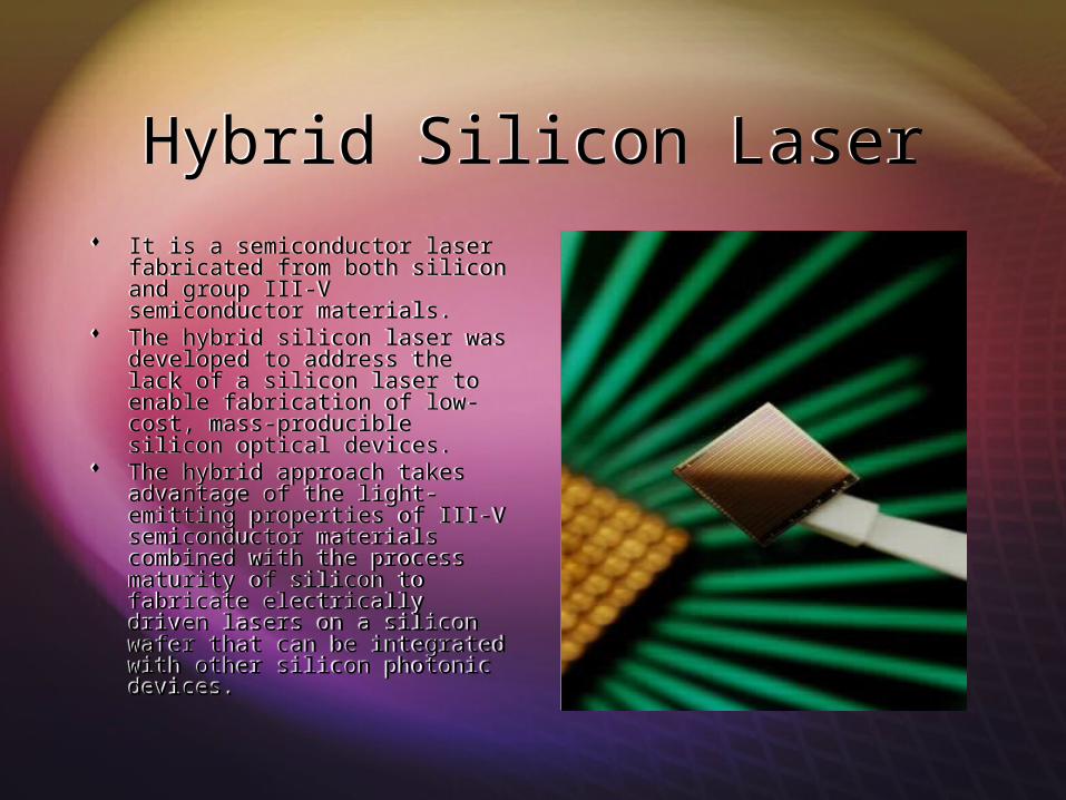
Hybrid Silicon LaserHybrid Silicon Laser It is a semiconductor laser
fabricated from both silicon and group III-V semiconductor materials.
The hybrid silicon laser was developed to address the lack of a silicon laser to enable fabrication of low-cost, mass-producible silicon optical devices.
The hybrid approach takes advantage of the light-emitting properties of III-V semiconductor materials combined with the process maturity of silicon to fabricate electrically driven lasers on a silicon wafer that can be integrated with other silicon photonic devices.
It is a semiconductor laser fabricated from both silicon and group III-V semiconductor materials.
The hybrid silicon laser was developed to address the lack of a silicon laser to enable fabrication of low-cost, mass-producible silicon optical devices.
The hybrid approach takes advantage of the light-emitting properties of III-V semiconductor materials combined with the process maturity of silicon to fabricate electrically driven lasers on a silicon wafer that can be integrated with other silicon photonic devices.
Fabrication of Hybrid Silicon Laser
Fabrication of Hybrid Silicon Laser
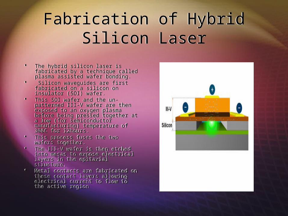
The hybrid silicon laser is fabricated by a technique called plasma assisted wafer bonding.
Silicon waveguides are first fabricated on a silicon on insulator (SOI) wafer.
This SOI wafer and the un-patterned III-V wafer are then exposed to an oxygen plasma before being pressed together at a low (for semiconductor manufacturing) temperature of 300C for 12hours.
This process fuses the two wafers together.
The III-V wafer is then etched into mesas to expose electrical layers in the epitaxial structure.
Metal contacts are fabricated on these contact layers allowing electrical current to flow to the active region
Applications of Hybrid Silicon Laser
Applications of Hybrid Silicon Laser
Intel suggests this light source could be used for optical communications when integrated with silicon photonics.
Silicon manufacturing and fabrication is widely used in the electronic industry to mass-produce low-cost electronic devices.
Silicon photonics uses these same electronic manufacturing technologies to make low cost integrated optical devices.
By using this wafer bonding technique many hybrid silicon lasers can be fabricated simultaneously on a silicon wafer, all aligned to the silicon photonic devices.
Potential uses cited in the references below include fabricating many, possibly 100’s of hybrid silicon lasers on a die and using silicon photonics to combine them together to form high bandwidth optical links for personal computers, servers or back planes.

Problems in making silicon lasers:Problems in making silicon lasers:
Unlike the III-V compounds, such as gallium arsenide, generally used to make semiconductor lasers, silicon has an indirect bandgap. That means the momentum of the charge carriers—negative electrons and positive holes—do not match, and when they combine they are more likely to produce a vibration than a photon.
Unlike the III-V compounds, such as gallium arsenide, generally used to make semiconductor lasers, silicon has an indirect bandgap. That means the momentum of the charge carriers—negative electrons and positive holes—do not match, and when they combine they are more likely to produce a vibration than a photon.
Using Raman EffectUsing Raman Effect
Intel researchers used an external light source to "pump" light into their chip. The natural atomic vibrations in silicon amplify the light as it passes through the chip. This amplification is called the Raman effect.But, increasing the light pump power beyond a certain point no longer increased amplification and eventually even decreased it. The reason was a physical process called "Two-Photon Absorption" .
Intel researchers used an external light source to "pump" light into their chip. The natural atomic vibrations in silicon amplify the light as it passes through the chip. This amplification is called the Raman effect.But, increasing the light pump power beyond a certain point no longer increased amplification and eventually even decreased it. The reason was a physical process called "Two-Photon Absorption" .

SolutionSolution
To integrate a semiconductor structure, PIN (P-type - Intrinsic - N-type) device into the waveguide. When a voltage is applied to the PIN, it acts like a vacuum and removes most of the excess electrons from the light's path. The PIN device combined with the Raman effect produces a continuous laser beam.
To integrate a semiconductor structure, PIN (P-type - Intrinsic - N-type) device into the waveguide. When a voltage is applied to the PIN, it acts like a vacuum and removes most of the excess electrons from the light's path. The PIN device combined with the Raman effect produces a continuous laser beam.