Silicon Carbide Sensors and Electronics for Harsh ... · PDF fileSilicon Carbide Sensors and...
18
Silicon Carbide Sensors and Electronics for Harsh Environment Applications Laura J. Evans NASA Glenn Research Center Cleveland, OH 44135 Silicon carbide (SiC) semiconductor has been studied for electronic and sensing applications in extreme environment (high temperature, extreme vibration, harsh chemical media, and high radiation) that is beyond the capability of conventional semiconductors such as silicon. This is due to its near inert chemistry, superior thermomechanical and electronic properties that include high breakdown voltage and wide bandgap. An overview of SiC sensors and electronics work ongoing at NASA Glenn Research Center (NASA GRC) will be presented. The main focus will be two technologies currently being investigated: 1) harsh environment SiC pressure transducers and 2) high temperature SiC electronics. Work highlighted will include the design, fabrication, and application of SiC sensors and electronics, with recent advancements in state-of-the-art discussed as well. These combined technologies are studied for the goal of developing advanced capabilities for measurement and control of aeropropulsion systems, as well as enhancing tools for exploration systems. https://ntrs.nasa.gov/search.jsp?R=20080005539 2018-04-27T00:30:48+00:00Z
Transcript of Silicon Carbide Sensors and Electronics for Harsh ... · PDF fileSilicon Carbide Sensors and...

Silicon Carbide Sensors and Electronics for Harsh Environment Applications
Laura J. Evans NASA Glenn Research Center
Cleveland, OH 44135 Silicon carbide (SiC) semiconductor has been studied for electronic and sensing applications in extreme environment (high temperature, extreme vibration, harsh chemical media, and high radiation) that is beyond the capability of conventional semiconductors such as silicon. This is due to its near inert chemistry, superior thermomechanical and electronic properties that include high breakdown voltage and wide bandgap. An overview of SiC sensors and electronics work ongoing at NASA Glenn Research Center (NASA GRC) will be presented. The main focus will be two technologies currently being investigated: 1) harsh environment SiC pressure transducers and 2) high temperature SiC electronics. Work highlighted will include the design, fabrication, and application of SiC sensors and electronics, with recent advancements in state-of-the-art discussed as well. These combined technologies are studied for the goal of developing advanced capabilities for measurement and control of aeropropulsion systems, as well as enhancing tools for exploration systems.
https://ntrs.nasa.gov/search.jsp?R=20080005539 2018-04-27T00:30:48+00:00Z

1Glenn Research Center atLewis Field
Silicon Carbide Sensors and Electronics forHarsh Environment Applications
Laura J. EvansNASA Glenn Research Center
Cleveland, OH
http://www.grc.nasa.gov/WWW/SiC/Sensors World Conference Dec. 13, 2007
Williamsburg, VA
2Glenn Research Center atLewis Field
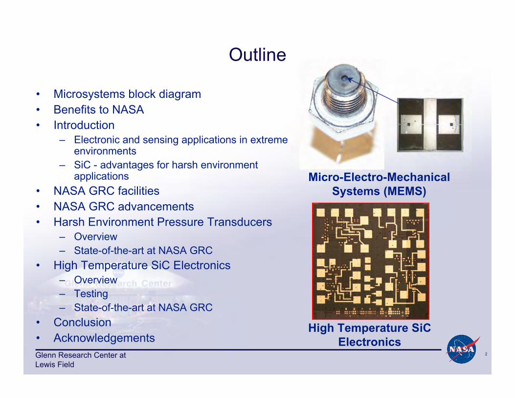
Outline
High Temperature SiCElectronics
Micro-Electro-MechanicalSystems (MEMS)
• Microsystems block diagram• Benefits to NASA• Introduction
– Electronic and sensing applications in extremeenvironments
– SiC - advantages for harsh environmentapplications
• NASA GRC facilities• NASA GRC advancements• Harsh Environment Pressure Transducers
– Overview– State-of-the-art at NASA GRC
• High Temperature SiC Electronics– Overview– Testing– State-of-the-art at NASA GRC
• Conclusion• Acknowledgements

3Glenn Research Center atLewis Field
ACTUATORS
S
EN
SOR
S
Phys
ical
/Che
mic
al S
igna
l
Communication
POWER
Mec
hani
cal/E
lect
rica
l/Opt
ical
Syst
em O
utpu
t
Electrical/OpticalControl & Communication
AnalogSignal
Processing
DigitalSignal
Processing
Large-scale integrated electronics crucial to highly advanced MEMS.
Microsystem Block Diagram

4Glenn Research Center atLewis Field
Intelligent Propulsion Systems
Some of these applications require prolonged T > 400 °C operation
Space Exploration Vision: PowerManagement and Distribution
Venus ExplorationMore Electric + Distributed Control Aircraft
High Temperature MEMS and Electronics Benefits to NASA

5Glenn Research Center atLewis Field
Applications
Harsh EnvironmentPackaging
(2000 hours at 500 °C)
Range of Physical and Chemical Sensorsfor Harsh Environments
High TemperatureSignal Processing
and Wireless
Long Term: HighTemperature “Lickand Stick” Systems
• Applications in environments of high temperature,extreme vibration, harsh chemical media, high radiation– Measurement and control of challenging systems
• Aircraft engines• Automotive• Well drilling
– Enhanced tools for exploration systems• Requires development of integrated sensors, electronics,
and packaging

6Glenn Research Center atLewis Field
Technologies for Harsh Environments• Current technology - suitable up to 350 °C:
– T < 150 °C (302 °F), silicon is used in almost all integrated circuits in usetoday.
– T < 300 °C (572 °F), well-developed Silicon-On-Insulator (SOI) IC’savailable for low-power logic and signal processing functions.
– T > 350 °C (662 °F), other wide-bandgap semiconductors such as SiC,GaN, or diamond are needed.
• Why SiC for harsh environments?– Near inert chemistry due to high bonding energy– Similar processing as silicon– Technology at a level where single crystal wafers can be purchased– Superior thermomechanical properties (greater hardness, higher Young’s
modulus, high thermal conductivity)– Superior electronic properties (wide bandgap, high breakdown electric
field, high carrier saturation velocity)• Benefits:
– Improved reliability– Reduced cooling system: reduced cost, volume, and weight of control
systems, reduction in fuel consumption and pollution– Direct sensing and control in harsh environment e.g. turbine engine
7Glenn Research Center atLewis Field
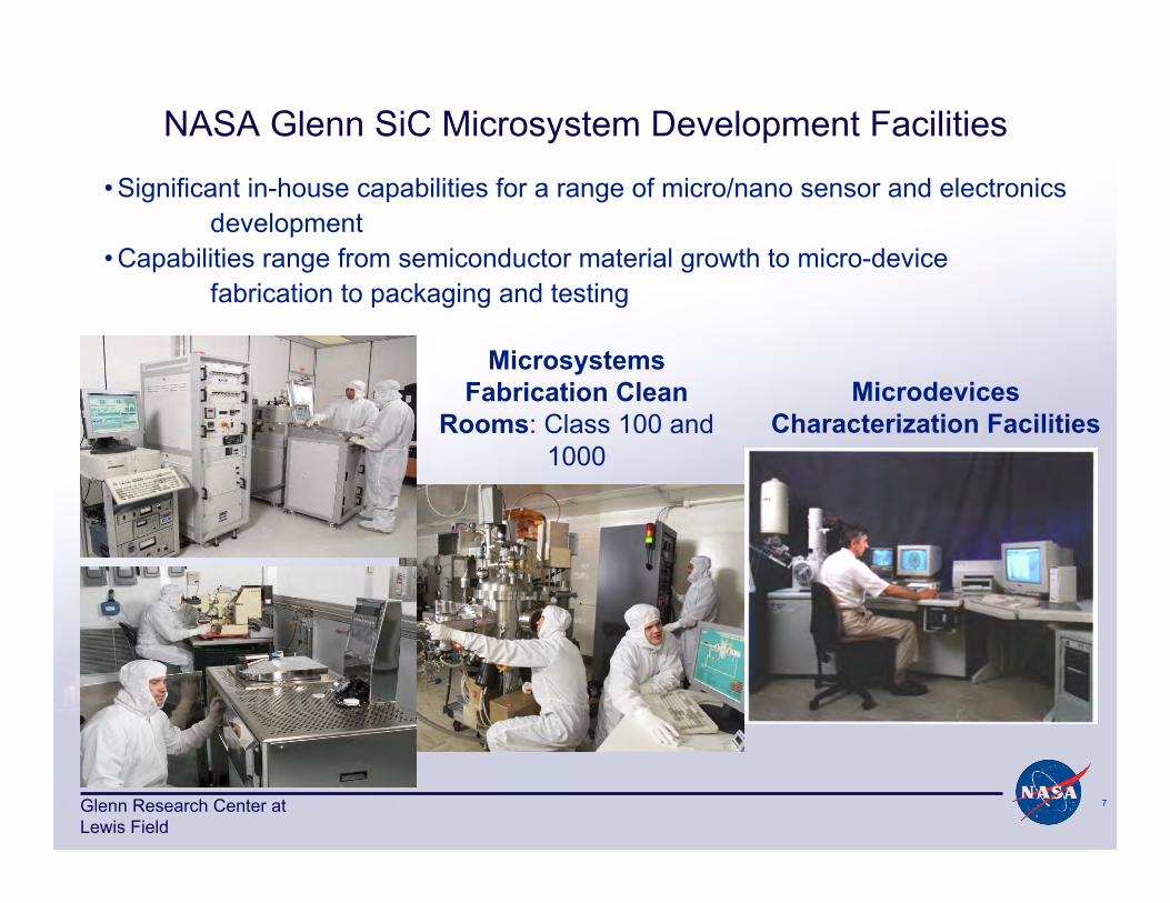
• Significant in-house capabilities for a range of micro/nano sensor and electronicsdevelopment
• Capabilities range from semiconductor material growth to micro-device fabrication to packaging and testing
MicrodevicesCharacterization Facilities
MicrosystemsFabrication Clean
Rooms: Class 100 and1000
NASA Glenn SiC Microsystem Development Facilities

8Glenn Research Center atLewis Field
500 °C Durable ChipPackaging
And Circuit Boards(L. Chen, 2002 GRC R&T
Report)
500 °C Durable Metal-SiCContacts
(R. Okojie, 2000 GRC R&TReport)
Key fundamental high temperature electronic materials and processingchallenges have been faced and overcome by systematic basicmaterials processing research (fabrication and characterization).
Additional advancements in device design, insulator processing, etc., also made.
100 µm
Improvements in SiCMicrofabrication Processes(L. Evans, 2006 GRC R&T
Report)
Previous Key NASA Glenn Advancements

9Glenn Research Center atLewis Field
Objective:Develop high temperature (500 to 600 °C)
SiC pressure sensors for: Engine health monitoring with wireless
data transmission Active combustion control
Harsh Environment SiC Pressure Sensors: an Overview
Challenges: Reliable device packaging: failure at
wire bonds Failure due to strains/stresses caused
by CTE mismatch duringheating/cooling
Premature failure of diaphragms due tostress concentration
500 °C SiC pressure sensor
Real world application: pressuresensor installed in engine test

10Glenn Research Center atLewis Field
MEMS-DCA Sensor Attributes: Eliminates failures associated with wire bonds
at high temperature Reduces thermomechanical stress by
decoupling sensor from package
SensorGlass sealedGap
AlN
Kovar tube
Contact wire
Thermocouplehole
Reference cavity
MEMS-DCA (Direct Chip Attach) packagedSiC pressure sensor
Net output voltage of three SiC pressuresensors tested up to 600 °C
0
1
2
3
4
5
6
7
0 20 40 60 80 100Pressure (psi)
Net
Out
put (
mV
)
Sensor 73 (25C)Sensor 74 (25C)Sensor 73 (600C)Sensor 74 (600C)Sensor 75 (25C)Sensor 75 (600C)
Harsh Environment SiC Pressure Sensors
11Glenn Research Center atLewis Field
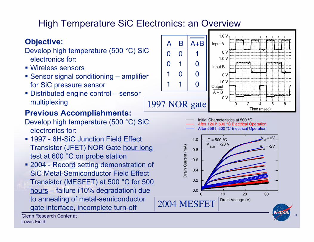
Objective:Develop high temperature (500 °C) SiC
electronics for: Wireless sensors Sensor signal conditioning – amplifier
for SiC pressure sensor Distributed engine control – sensor
multiplexing
0.0
0.2
0.4
0.6
0.8
1.0
0 10 20 30
Drai
n Cu
rrent
(mA)
Drain Voltage (V)
VG
= 0V
VG
= -2V
After 126 h 500 °C Electrical OperationInitial Characteristics at 500 °C
T = 500 °CV
Sub = -20 V
After 558 h 500 °C Electrical Operation
Previous Accomplishments:Develop high temperature (500 °C) SiC
electronics for: 1997 - 6H-SiC Junction Field Effect
Transistor (JFET) NOR Gate hour longtest at 600 °C on probe station
2004 - Record setting demonstration ofSiC Metal-Semiconductor Field EffectTransistor (MESFET) at 500 °C for 500hours – failure (10% degradation) dueto annealing of metal-semiconductorgate interface, incomplete turn-off
A B A+B0 0 10 1 01 0 01 1 0
0 2 4 6 8
Time (msec)
0 V
1.0 V
0 V
1.0 V
0 V
1.0 V
Output
A + B
Input A
Input B
High Temperature SiC Electronics: an Overview
1997 NOR gate
2004 MESFET

12Glenn Research Center atLewis Field
Current-voltage characteristics are very good and stable after 3000 hoursEnables realization of analog integrated circuits (amplifiers, oscillators)
Excellent turn-off characteristics, ON to OFF current ratioEnables realization of digital circuits.
Less than 7% change occurs during 3000 hours at 500 °C. - 7% change is smaller than listed on most silicon transistor specs sheets.
NASA Glenn Discrete SiC JFET Transistors: First to Surpass3000 Hours of Stable Electrical Operation at 500 °C
100 µm
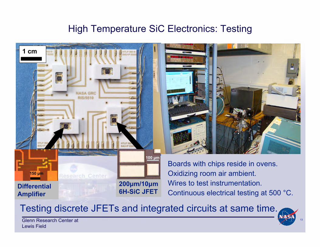
13Glenn Research Center atLewis Field
1 cm
200µm/10µm6H-SiC JFET
100 µm
150 µm
DifferentialAmplifier
Boards with chips reside in ovens.
Continuous electrical testing at 500 °C.Wires to test instrumentation.Oxidizing room air ambient.
Testing discrete JFETs and integrated circuits at same time.
High Temperature SiC Electronics: Testing
14Glenn Research Center atLewis Field
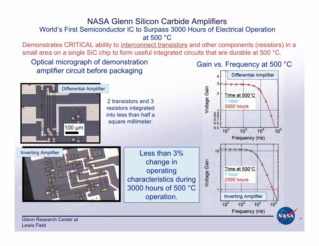
100 µm
World’s First Semiconductor IC to Surpass 3000 Hours of Electrical Operationat 500 °C
Demonstrates CRITICAL ability to interconnect transistors and other components (resistors) in asmall area on a single SiC chip to form useful integrated circuits that are durable at 500 °C.
Optical micrograph of demonstrationamplifier circuit before packaging
Gain vs. Frequency at 500 °C
2 transistors and 3resistors integratedinto less than half asquare millimeter.
Less than 3%change inoperating
characteristics during3000 hours of 500 °C
operation.
NASA Glenn Silicon Carbide Amplifiers
Inverting Amplifier
Differential Amplifier
15Glenn Research Center atLewis Field
Conclusion
• Future work:– Continuation of high temperature testing– Continued improvement of fabrication procedures– Fabrication of improved devices based on knowledge
gained• Long term goals:
– Technology transfer in progress for SiC PressureTransducer work
– Technology transfer for SiC electronics work– Complete integration of electronics and sensors for
total harsh environment sensing capability– Continue to push the envelope of what is possible in
high temperature electronics and sensors, e.g., smartwireless sensor systems

16Glenn Research Center atLewis Field
Work is carried out at NASA GRC by:
• Glenn M. Beheim• Carl W. Chang• Liang-Yu Chen• Gary W. Hunter• Dorothy Lukco• Philip G. Neudeck• Robert S. Okojie• David J. Spry
• Charles A. Blaha• Jose M. Gonzalez• Kimala L. Laster• Lawrence G. Matus• Kelley M. Moses• Michelle M. Mrdenovich• Beth A. Osborn• Andrew J. Trunek
Acknowledgements

17Glenn Research Center atLewis Field
The work in this talk has been supported by NASA’s AeronauticsResearch Mission Directorate:
• IVHM: Integrated Vehicle Health Management• Supersonics• Hypersonics• Subsonic Fixed Wing• Subsonic Rotary Wing
Recent press releases:http://www.nasa.gov/centers/glenn/news/pressrel/2007/07053_patents.html
http://www.nasa.gov/centers/glenn/news/pressrel/2007/07035_Electric_Chip.html
NASA Funding