Fabrication and Characterization of Single-Crystal Silicon ...

Silicon Bottom Subcell Fabrication, Loss Analysis and ShuntIdentification for Two-Terminal Multijunction Solar Cells
by MASSACHUSET0TISTITUTEOF TECHNOLOGY
Juan Felipe Oviedo Perhavec JUNO10YJUN 2 1 2017
B.S. in Mechanical EngineeringUniversidad San Francisco de Quito, 2014 LIBRARIES
Submitted to the Department of Mechanical Engineering ARCHIVES
in partial fulfillment of the requirements for the degree ofMaster of Science in Mechanical Engineering
at the
MASSACHUSETTS INSTITUTE OF TECHNOLOGY
June 2017
2017 Massachusetts Institute of Technology. All rights reserved.
Signature redactedA u th o r ...................................... ...... ...........--- ---
an Felipe Oviedo PerhavecDepartment of Mechanical Engineering
May 12, 2017
Certified by...............................................Signature redactedTonio Buonassisi
Associate Professor of Mechanical Engineering
, jThesis Co-Supervisor
Signature redactedIan Marius Peters
Research Scientist in Mechanical Engineering DepartmentThesis Co-Seupervisor
Accepted by.......................................Signature redactedRohan Abeyaratne
Quentin Berg Professor of MechanicsChairman, Committee on Graduate Students

2

Silicon Bottom Subcell Fabrication, Loss Analysis and ShuntIdentification for Two-Terminal Multijunction Solar Cells
by
Juan Felipe Oviedo Perhavec
Submitted to the Department of Mechanical Engineeringon May 12 th, 2017, in partial fulfillmentof the requirements for the degree of
Master of Science in Mechanical Engineering
Abstract
Two-terminal multijunction solar cells are a promising technology to surpass the
energy-conversion efficiency of commercial single junction devices. Multijunction solar
cells that integrate silicon bottom subcells could allow cost-effective efficiency
enhancements and further growth in the worldwide installed photovoltaic capacity.
However, the fabrication and characterization of multijunction devices is more complex
than the standard single junction case, due to optical, electrical and architecture
constraints. In this context, this thesis proposes and tests methods for fabrication and
characterization of two-terminal multijunction devices, with special emphasis in the
bottom silicon subcells.
A low-capex, local area back-surface field, silicon cell is adapted for operation in a
two-terminal perovskite-silicon tandem device. A contactless voltage loss analysis
methodology is developed, and used to optimize the tunnel junction of the device. Finally,a general methodology to identify the shunted cells in two-terminal tandem devices is
developed and validated in GaAs/GaAs tandem device. These characterization
methodologies allow an adequate diagnosis of quality issues in multijunction solar cells,
and provide useful tools for future efficiency improvements.
Thesis Co-Supervisor: Tonio Buonassisi
Title: Associate Professor of Mechanical Engineering
Thesis Co-Supervisor: Ian Marius Peters
Title: Research Scientist in Mechanical Engineering Department
3

4

AcknowledgementsOn ne dscouvre pas de terre nouvelle sans consentir A
perdre de vue, d'abord et Iongtemps, tout rivage.
Andr6 Gide
This work has been made possible by the intellectual, financial and personalsupport of numerous persons and institutions around the globe. Here, I wouldlike to express my unending gratitude to all of you.
First, I would like to recognize the support and guidance of all my fellow PVLab and SMART members which whom I had the luck to collaborate and, also,mentored me. In particular, I want to acknowledge my two advisors, Prof.Tonio Buonassisi and Dr. Marius Peters. Both have been tremendouslygenerous, patient and supportive during my time at MIT. Your constantattention to my professional and personal development is remarkable. I wouldalso like to recognize all my lab mates, specially Jonathan Mailoa, Sarah Sofia,Robert Hoye, Riley Brandt, Liu Zhe, Mallory Jensen, Sterling Watson, ErinLooney in Boston and Ren Zekun, Maung Thway, Xin Hang in Singapore,whom helped me to define my intellectual pathway and to greatly enjoy mytime at MIT. Financially, I would like to acknowledge the generous support ofthe MIT-SMART initiative and the U.S. DOE through the NextGen III grant.
Leaving a comfortable job, your country and your culture and come to MIT isa great challenge. The support of multiple friends scattered around the worldhas been essential during this time. Gratitude is too big and words too limitedto properly thank you all. Among many, I would like to mention: Dave,Miguel, Paola, Camila, Francis, Xavier, John, Fernando, Sabah, Quinti, Luis,Marcos, PK, Andrew and many others.
Finally, and most important, I would like to thank my family in Ecuador,specially Edmundo, Adriana and Gabriela. Your outstanding resilience,constant sacrifice and unconditional love have been indispensable duringthese years in the United States. You are always my inspiration and myexample.
Thank you all.
5

Contents
Contents 6
List of Figures 8
List of Tables 9
CHAPTER 1 10
1.1 Motivation 10
1.2 Multijunction Solar Cells 12
1.3 Goals and Thesis Structure 16
1.4 Prior Art of Two-Terminal Multijunction Devices 17
CHAPTER 2 20
2.1 Device Requirements 20
2.2 Bottom Cell Types 22
2.3 Full-area BSF Fabrication 24
2.4 Local-area BSF Fabrication 25
2.4.2 Fabrication results and loss analysis for reference samples 29
2.4.3 Tunnel junction deposition 32
CHAPTER 3 34
3.1 Subcell loss analysis methodologies 34
3.2 Voltage loss analysis of bottom subcell 36
3.2.1 Methodology 36
3.2.2 Voltage Loss Breakdown 43
3.2.3 Improving the Si/ ITO-interlayer 46
3.2.4 Pathways for perovskite top cell analysis 48
CHAPTER 4 50
4.1 Shunts in Multijunction Solar Cells 50
4.2 Sentaurus TCAD simulation and equivalent circuit model of 2T multijunctiondevice 52
4.3 f-V curves under various current matching and shunting conditions 56
4.4 Experimental validation 6o
6

4.4.1 Measurement of 3T device 6o
4.4.2 Spectrometric characterization 63
CHAPTER 5 70
References 75
7
List of Figures
Figure i: Required scenarios of PV installed capacity to reach the climate targets. Plot
taken from [3]-------------..........--.....---------------------------------...........................................................11
Figure 2: Schematic of light absorption in multijunction solar cell. Graph made for PV
Education, courtesy of Sarah Sofia (M IT PV Lab)............................................................ 13
Figure 3: Tandem architectures and equivalent circuits. Graph made for PV Education,courtesy of Sarah Sofia (M IT PV Lab)................................................................................ 14
Figure 4: Tandem detailed-balance efficiency limit map for double junction (a) series-
connected two-terminal tandems, and (b) mechanically-stacked, four-terminal tandems.
Graph made for PV Education, courtesy of Sarah Sofia (MIT PV Lab)............................. 15
Figure 5: Perovskite-Si 2T tandem device with generic p-type Si bottom subcell. ............. 20
Figure 6: BSF and LBSF silicon cells.................................................................................. 23
Figure 7: J-V characteristics of full-area BSF device...........................................................25Figure 8: External Quantum Efficiency (EQE) of full-area BSF device. ............... 25
Figure 9: Lifetime as a function of excess carrier concentration for three test wafers
w ithout a diffused junction ................................................................................................... 26
Figure 10: Test samples and fabrication steps for Si bottom subcell.................28Figure ii: Lifetime PL image of wafer with diffused junction .......................................... 29
Figure 12: Current loss and fill factor loss breakdown of single junction reference cells.... 31Figure 13: Pseudo J-V curves for bottom Si cells, after a) ITO deposition, b) NiOx
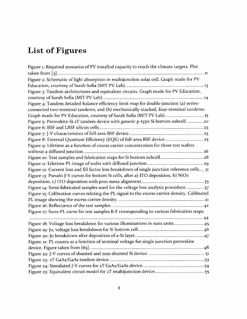
deposition, c) ITO deposition with poor mesa alignment................................................33Figure 14: Semi-fabricated samples used for the voltage loss analysis procedure...........37Figure 15: Calibration curves relating the PL signal to the excess carrier density. Calibrated
PL im age showing the excess carrier density. .................................................................... 41Figure 16: Reflectance of the test sam ples. ........................................................................ 42
Figure 17: Suns-PL curve for test samples B-F corresponding to various fabrication steps.
................................................................................................................................................ 4 4Figure 18: Voltage loss breakdown for various illuminations in suns units.....................45Figure i9: Jo, voltage loss breakdown for Si bottom cell...................................................... 46
Figure 20: Jo breakdown after deposition of a-Si layer. ................................................... 47Figure 21: PL counts as a function of terminal voltage for single junction perovskite
device. Figure taken from [65]--------------------------------------------------............................................. 48
Figure 22: J-V curves of shunted and non-shunted Si device. .......................................... 51Figure 23: 2T GaAs/GaAs tandem device............................................................................ 53Figure 24: Simulated J-V curves for 2T GaAs/GaAs device. ............................................. 54Figure 25: Equivalent circuit model for 2T multijunction device.........................................55
8

Figure 26: J-V curves for different shunting and current limitation conditions. A moderatecurrent m ismatch between subcells is assum ed. ............................................................. 57Figure 27: J-V characteristics for various shunting and current limitation conditions.Severe m ism atch between subcells is supposed............................................................... 58Figure 28: Fill factor of the 2T tandem device as a function of shunt resistance. ........... 59Figure 29: Measured J-V curves of the 2T GaAs/GaAs device and its subcells. .............. 62
Figure 30: LED spectra of the equal irradiance level and different APE values,approximating real spectra measured in Singapore........................................................ 65Figure 31: J-V characteristics of GaAs/GaAs dual junction structure under varying APEsp e ctra . .................................................................................................................................... 6 7Figure 32: Measured and simulated J-V curves of cell at APE values of 1.71 and 1.95 eV.... 68
List of Tables
Table i: Reference single junction device parameters for various samples and firingco n d itio n s............................................................................................................................... 2 9
Table 2: Device parameters of reference single junction cell and wafer..........................38Table 3: Measurement plan for the voltage loss analysis procedure...............................39Table 4: Ratios between absorptance of calibration sample and individual test samples. .42
Table 5: Subcell and tandem device characteristics..............................................................55Table 6: Input parameters and characteristics of GaAs/GaAs device at standard conditions(A M I-5 G )................................................................................................................................ 6 6
9

CHAPTER 1
1 INTRODUCTION
i.i Motivation
In the Paris Climate Agreement, the scientific community and policymakers define 2 'C
as a threshold for global warming caused by greenhouse gas emissions from human origin,
and recommend to purse efforts to limit the warming to 1.5 0C or less [1], [2]. To achieve
this goal and mitigate the most harmful effects of climate change, a significant reduction
in greenhouse gas emissions has to occur in the next 15 years [3]. One main way of sharply
reducing energy emissions consists in the wide deployment of renewable energy sources,
especially solar photovoltaic (PV) and wind power, two of the most market-mature
renewable energy technologies. In the case of solar PV, it has been estimated that as much
as 10 TW of energy generation capacity have to be installed worldwide in order to reach
the emission reductions target [3]. To achieve this, the cost of solar energy needs to drop
significantly in the next decade, solar cell efficiencies have to experience substantial gains
and the manufacturing capacity has to be drastically expanded. Figure i shows the PV
installed capacity required to reach the climate targets of the Paris Agreement. The various
lines in the graph represent different pathways to reach the climate goals in the next 15
years. It is observed that a new high-efficiency advanced concepts are required to expand
photovoltaic energy generation to the required levels.
10

12- 0 climate targets
high-eff. advanced concept
10 - low-var. cost advanced conceptincreased debtline-of-sight
in=baseline
6
02016 2018 2020 2022 2024 2026 2028 2030
year
Figure 1: Required scenarios of PV installed capacity to reach the climate targets. Plot taken from [3].
The solar-generated electricity cost is very sensitive to changes in the energy-conversion
efficiency. Higher efficiencies achieved with little additional cost constitute a growth lever
of new photovoltaic installations. Various sensitivity analyses of the minimum sustainable
price (MSP) of crystalline silicon modules showed that increments in efficiency are among
the most significant variables determining the price per module, given usually in dollars-
per-watt ($/W) [41, [5]. This fact is a consequence of the $/W price being a function of the
inverse of the module capacity. In addition to the module cost, if high efficiency is achieved
with little additional cost, the fixed and variable costs of the system's components and its
installation are reduced, which represent more than 6o% of the total system cost for
residential systems and 40% for utility-scale PV installations.
In spite of its potential, substantial efficiency improvements of. most established
commercial single junction technologies have proven challenging in recent years. For
example, the efficiency of crystalline silicon (c-Si) single junction devices has gone from
25% to 26.6% in the last fifteen years [6]. The efficiency improvements have been
constrained both by the state of the current technologies, the cost-competitiveness of
11

high-efficiency architectures and the excessive capital cost of launching or renewing
manufacturing facilities, which reduce the relative economic benefit for the manufacturer
(in ROI terms) of higher efficiencies [3]. In this context, certain multijuction solar cells
constitute an opportunity to surpass the practical limits of single junction solar cells and
further reduce photovoltaic energy cost. In order to achieve this, the multijunction
technologies have to be able to provide an efficiency improvement compared to single
junction architectures at little or no additional cost. The multijunction architectures that
require low capital expenditure and lever on the main technologies in the market are the
most likely ones to satisfy the cost requirement. For instance, multijunction devices that
integrate p-type Si industrial diffused junction subcells in combination with inexpensive,
highly-efficient top subcells (such as perovskite or other thin-film materials) have a high
chance of being cost-efficient.
In this context, this thesis focuses on two-terminal perovskite-Si tandem devices, using
a low capital expenditure p-type Si cell. The work addresses fabrication, loss analysis and
shunt characterization of multijunction devices. The final goal of the thesis is to provide
methodologies and tools to fabricate and analyze multijunction devices for future potential
market applications.
1.2 Multijunction Solar Cells
In general, the theoretical maximum efficiency of a solar cell is limited by the fraction of
photons of the solar spectrum that can be absorbed by the material, generating
electron-hole pairs, and then can be extracted as electric energy [7], [8]. Photons with
energies below the bandgap of the material cannot be absorbed, whereas photons with
energies above the bandgap are absorbed, but the excited electron-hole pair dissipates the
excess energy as heat [9]. The latter loss mechanism is known as thermalization, and limits
the voltage of the device. On the other hand, the loss due to low energy photons limits the
number of photons captured, or the actual current of the device. In consequence, an
absorber material of a certain bandgap determines a trade-off between the number and the
energy of electron-hole pairs generated. The quantification of these mentioned losses for a
12

certain bandgap, in combination with radiative recombination, constitutes the
Shocldey-Queisser detailed-balance limit for solar cell efficiency [8]. For single junction
solar cells with the most beneficial bandgap figure, the Shocldey-Queisser limit is 33.7% [10]
for the standard AM I-5G spectrum [n].
Multijunction solar cells, also commonly known as tandem devices, combine two or more
stacked absorber materials with complementary bandgaps to capture the solar spectrum.
more efficiently and, in consequence, reach a higher energy-conversion efficiency compared
to single junction devices [12]. Figure 2 shows a schematic of a multijunction device with two
junctions, in which different subcells absorb complementary parts of the solar spectrum.
High E, Top Cell
Low E. Top Cell
Figure 2: Schematic of light absorption in multijunction solar cell. Graph made for PVEducation, courtesy ofSarah Sofia (MIT PV Lab).
In this case, the material of lower bandgap provides a wide spectral absorption range,
while the material of a higher bandgap captures the high energy photons of the spectrum
more efficiently [13], [14]. As a results, the device is able to harvest the energy of the solar
spectrum more efficiently. The Shockley-Queisser limit in this case, for the bandgap
combination that maximizes the efficiency, is around 42% under AM 1. 5G illumination [13].
Depending on the coupling mechanism between subcells, we mainly distinguish between
two multijunction architectures: mechanically-stacked 4-terminal (4T) tandems, in which
subcells are optically coupled but electrically isolated from each other, and monolithic
2-terminal (2T) tandems, which are optically and electrically coupled [6], [15]. The electrical
13

coupling in a 2T device is achieved by using a tunnel junction or a recombination layer. As
shown in Figure 3, the tunnel junction corresponds to a highly doped area between the top
and the bottom subcells. One part of the tunnel junction is n-doped, whereas the other part
is p-doped. The sudden change in the band diagrams of the cell causes quantum tunneling
in the interface. The tunneling phenomenon allows the recombination of an electron-hole
pair in the tunnel junction, thus allowing the flow of current through the cell and connecting
both subcells in series. The total current density in this case is limited by the smallest current
density of any subcell of the device. In consequence, to achieve the maximum efficiency in
a 2T device, the currents at the maximum power point of the top and bottom subcell must
be equal. This requirement is commonly known as current-matching [16], [17]. The 4 T
architecture, on the other hand, has a separate circuit for each subcell in the stack. A
transparent insulating layer between the top and bottom subcell is required to allow the pass
of low energy photons to the bottom subcell.
2-Terminal
.
<]
RSTJ +
Figure 3: Tandem architectures and equivalent circuits. Graph(MIT PV Lab).
4-Terminal
Transparent_6insulator 7
Bottom cell
d PVop
made for P VEducation, courtesy of Sarah Sofia
The inherent conditions, such as filtered spectrum, reduction in illumination intensity,
current mismatch between subcells or presence of the tunnel junction, determine different
14
4)
4)(.2
.2(.24)
03
20
E54
-4)'J Z6

design constraints and performance characteristics [18]. The 2T and 4 T architectures have
different theoretical and practical performances according to the bandgap of the subcells
and the solar spectrum conditions. The current-matching requirement in the case of the 2T
multijunction devices limits the available bandgap for which it is possible to achieve
high-efficiency. Figure 4 shows the maximum theoretical efficiency for the 2T and 4T
architectures as a function of the bandgap of the top subcell or the bottom subcell under
AM 1. 5 G conditions. The 2T tandem device has a narrower range of bandgaps for which the
efficiency is high compared to the 4T architecture. This fact reduces the number of possible
suitable absorber materials for a 2T tandem device. In this case, materials with tunable
bandgaps become important, such as perovskites, organic or perovskite-inspired absorber
materials for which the bandgap is usually tunable through variations in the stoichiometry
[15].
3 % 340 40
2.5 35 C2.5 35
CUC
20 1.5 20
15 15
2.5 5100^ 1 15 2 . 5 0.5 1 1.5 2 2.5 3
Top-cell band gap [eV] Top-cel band gap [eV]
(a) 2-Terminal (b) 4-Terminal
Figure 4: Tandem detailed-balance efficiency limit map for double junction (a) series-connected two-terminaltandems, and (b) mechanically-stacked, four-terminal tandems. Graph made for PVEducaton, courtesy of SarahSofia (MIT PV Lab).
Another relative disadvantage of 2T terminal architectures compared to 4T is the
sensitivity of the former to spectral conditions. Certain spectral conditions could reduce the
photogenerated current in the top or the bottom subcells, causing one subcell to become
15

current limiting and reduce the overall efficiency of the device For instance, for GaAs on Si
tandem device, the 4 T architecture was found to produce as much as 20% more energy
compared to the 2T architecture for specific spectrum conditions [19]. On the other hand,
4 T devices are usually more expensive and laborious to manufacture than 2T devices. They
require an extra set of contacts on the rear of the top subcell and on the front of the bottom
subcell. The rear contacts of the bottom subcell need to be transparent to allow photons to
reach the bottom subcell. For new absorber materials, especially thin-films, this
requirement usually represents a constraint as the absorber materials or architectures are
not compatible with some traditional semi-transparent contact materials or contact
manufacturing steps [15], [20]. Additionally, both subcells require to be mechanically
stacked and connected to additional power electronics. In consequence, there is a trade-off
between the manufacturability and the design and operation flexibility of 2T and 4T
multijunction architectures [21].
A process that limits or enhances the energy conversion efficiency is luminescence
coupling, or the process by which photons emitted by radiative recombination in the higher
bandgap subcell are absorbed by the lower bandgap subcell. Luminescent coupling increases
the photogenerated current in the subcell, and could change the expected current-matching
conditions. The process is common for absorber materials that present high radiative
recombination, such as III-V solar cells [22].
1.3 Goals and Thesis Structure
Due the cost advantages and manufacturing capacity of c-Si single junction solar cells,
c-Si bottom cells are envisioned to be adapted to novel two-terminal tandem architectures
in combination with top subcells of various types such as perovskites or III-V materials [6],
[23], [241. This thesis focuses on two-terminal c-Si based multijunction solar cells, with
special emphasis given to the industrial p-type, diffused junction, bottom Si subcell in a
tandem stack. As mentioned in the motivation section, this architecture was the
16

potentiality to achieve high-efficiency with little additional cost. The following goals are
accomplished in the respective chapters:
" In Chapter 2, the fabrication process and measurement of a two-terminal
perovskite-Si tandem is described Special attention is given to the design and
the fabrication of the Si bottom subcell to allow the tandem fabrication and
operation.
" In Chapter 3, the bottom Si subcell is characterized, and a contactless
methodology to perform an open-circuit voltage loss analysis is developed. The
methodology is used to characterize and optimize the tunnel junction of the
bottom subcell.
* In Chapter 4, an extended analysis of losses due to shunting in a
two-terminal tandem is performed under various current-matching conditions.
An equivalent circuit model of a two-terminal multijunction solar cells is
developed and the results area validated using a GaAs/GaAs solar cell.
The results provide adequate insights and tools for cell design, fabrication, loss
characterization and shunt identification of two-terminal multijunction devices that
include bottom Si subcells. The final goal of this work is to provide fabrication and
characterization methods for the development of efficient 2T multijunction devices.
1.4 Prior Art of Two-Terminal Multijunction Devices
Two-terminal monolithic multijunction devices have been widely used for applications
with a high-efficiency premium, such as III-V solar cells in the space industry. Triple
junction III-V concentrating solar cells surpassing 40% hold the world-record for
highest-efficiency for any device technology [25]. The III-V multijunction architectures
have been researched during several decades, and the fabrication and characterization
17

methods are well established. Some of the first III-V architectures were AlGaAs/GaAs and
GaInP/GaAs two-terminal solar cells. The first development of AlGaAs/GaAs were limited
to 20% efficiency because of difficulties in making stable tunnel junctions and the presence
of oxygen defects in the AlGaAs material [26]. Double hereto-structure tunnel junctions
were found useful for preventing diffusion from the tunnel junction into the structure and
achieving higher efficiencies [17]. Afterwards, two-terminal InGaP/GaAs and
InGaP/GaAs/Ge devices were realized by several improvements: a wide band-gap tunnel
junction with double hetero-structure that reduces absorption and recombination losses,
the use of InGaP/Ge hetero-face structure bottom cells, lattice matching of the Ge
substrate, widening of the top cell band gap by AlInGaP [17]. Some of the principles behind
these advanced were used to develop multiple novel architectures such as GaAs/GaAs,
GaAs/GaSb and InP/GaInAs, many of them surpassing 25% efficiency [27]. The use of a Si
bottom subcell or substrate instead of Ge has been proposed and realized for two-terminal
multijunction architectures by means of epitaxial liftoff [28] and wafer bonding [29].
For utility and residential applications, Si-based monolithic multijunction devices had
only recently became of interest. One of the most promising Si-based technologies is
perovskite-Si two-terminal tandems, due to the potential of perovskites as a low cost and
high-efficiency absorber materials. The first two-terminal 13.7% perovskite-silicon tandem
was reported in 2015, using an n-type diffused junction silicon bottom cell and an
amorphous Si (a-Si) tunnel junction [6]. A more efficient 18% perovskite-Si device was
fabricated using an n-type heterojunction with intrinsic silicon thin-layer (HIT) cell. The
authors adapted the perovskite deposition process for low temperatures (less than 250 0C)
to avoid amorphous silicon recrystallization, and used an ITO/SnO2 tunnel junction.
Werner et al. reported a monolithic tandem of 21.2% efficiency by using a more efficiency
n-type HIT cell and a tunnel junction with PEIE/PCBM instead of Sn02 [30]. Recently, a
23 .6%-efficient perovskite-Si tandem devices were reported using n-type heterojunction
with intrinsic silicon thin-layer (HIT) cells and an ITO/NiOx tunneling layer [24].
The future deployment of two-terminal perovskite-Si tandem devices requires
integration with p-type silicon solar cells, the dominant industrial Si cell type representing
18

over 85% percent of the global photovoltaics market. In consequence, low capital
expenditure perovskite-Si devices will require developing architectures that integrate well
with p-type bottom Si cells with diffused junctions. I focus in this work in the development
of a bottom Si subcell of these characteristics for a perovskite-Si device.
19

CHAPTER 2
2 FABRICATION OF THE BOTTOMSUBCELL
2.1 Device Requirements and Architecture
We integrated an industrial p-type Si subcell and a perovskite top subcell using a
NiOx/ITO tunnel junction. The architecture of the two-terminal multijunction perovskite-
Si device is shown in Figure 5.
p-type Si
Rear Contact
Figure 5: Perovskite-Si 2T tandem device with generic p-type Si bottom subcell.
Usually, perovskite devices have a hole transport layer (HTL) on the front surface of
the device and an electron transport layer (ETL) on the back, non-directly illuminated
surface. Thus, the top perovskite subcell in Figure 5, has an inverted architecture. This
architecture is required to adapt the successfully to the p-type Si bottom subcell.
20

As mentioned earlier, due to an abrupt change in the band diagram in the NiOx/ITO
interface, electrons and holes recombine in the tunnel junction. The recombination process
leaves a free hole in the bottom Si-subcell that is captured by the rear contact, whereas a
free electron is generated in the top perovskite subcell and captured by the electron
transport layer.
The top subcell is a 14.6% inverted perovskite device with stoichiometry of
Cs0 .17FAo.s3 Pb(Bro.17 o.83 )3 , which was chosen due to its higher stability and reduced
sensitivity to pinholes in large areas compared to the standard MAPbI 3 stoichiometry [24].
The electron transport layer on top was deposited through atomic layer deposition (ALD)
at low temperature. The transmittance of the NiOx/ITO interface was found to be more
than 95%, satisfactorily allowing light to reach the bottom Si subcell.
The industrial p-type subcell architecture has to be adapted to satisfy the following
requirements of the tandem device:
* Polished front surface: the NiOx layer and the perovskite cell are deposited by
spin coating and subsequent annealing. The spin coated layers commonly lack
uniformity when they are deposited over a non-planar surface. Perovskite solar cells
are prone to shunting due to pinholes created in non-uniform surfaces [311.
Furthermore, if perovskites are spin coated over textured surfaces, such as the
standard random texture front surfaces of p-type solar cells or, even, saw damage
etched surfaces, they are not functional due to the uneven distribution of material
across. In consequence, the perovskites top subcell requires to be deposited over a
polished, mirror-like front surface.
* ITO deposition: the ITO deposition is performed by sputtering. To avoid creating
pinholes during perovskite spin coating and avoid the insertion of a contact barrier
in the ITO interlayer, the Si cell front surface has be to free of particulate dust and
SiOx before the ITO deposition. To satisfy this quality requirement, the front surface
of the Si cell needs to be cleaned with a io% solution of HF and solvents before ITO
21

deposition. Additionally, the ITO deposition has to occur in an oxygen-free
atmosphere to avoid further formation of a SiOx on top of the device.
* Device mesa: the lateral current in the device has to be limited by means of a mesa
in order to achieve higher current densities. The mesa is a portion of the Si cell that
provides edge isolation to the device.
* High-efficiency: to achieve the highest possible efficiency, the bottom cell has to
reach a single junction efficiency close to industrial-quality p-type Si devices.
Additionally, the thickness and bandgap of the perovskite had to be adequately
tuned to match the current of both cell in the maximum power point.
* Low-capex: as mentioned in Chapter 1, many high-efficiency Si-based tandem
devices had been realized using high-efficiency HIT cells. However, a more suitable
pathway for potential commercialization of multijunction devices arguably requires
low capital expenditure intensity [3]. This requirement can be met by using existing
standard c-Si manufacturing capacity and developing multijunction architectures
that are compatible with the standard fabrication process.
2.2 Bottom Cell Types
Considering the device requirements, two different p-type Si solar cell architectures
were fabricated: back surface field (BSF) [32] and localized back surface field (LBSF) p-type
Si devices [331. Figure 6 shows a schematic of BSF and LBSF architectures. We adapted
these solar cells architectures to be integrated to perovskite multijunction architectures by
using front polished p-type wafers with a textured rear surface. The BSF and LBSF cells are
diffused junction solar cells with a fired aluminum (Al) contact in the back, which forms a
built-in electric p+ field on the rear surface of the solar cell [33]. This surface field allows a
substantial improvement in the cell performance, reducing the recombination losses at the
back surface and increasing the voltage of the solar cell compared to cells without BSF or
LBSF [32]. The BSF consists of a full-area of fired Al that forms a contact and passivates the
rear surface. The relatively simple deposition screen printing deposition process of full-area
22

Al and the quality of the passivation have made the BSF architecture ubiquitous in the
silicon solar cells market [341, 135]. However, the large area of the BSF contact contributes
to high minority carrier recombination and reduces the cell voltage. The local BSF cell, an
improved architecture capable of achieving higher voltage and energy-conversion
efficiency, was developed to solve this problem [33]. In the local BSF cell, the back surface
is passivated by a stack of AlOx and SiNx thin layers deposited through plasma-enhanced
chemically vapor deposition (PECVD). Afterwards, a full Al layer is deposited on the rear
passivated surface. To electrically contact the Al layer and the solar cell base, thin laser
scribes are made through the Al contact and the dielectric passivation layers. Finally, the
cell is fired to form the local p+ in the contacted area. A trade-off exists between the series
resistance of the contact and the surface recombination of the cell. A smaller contact area
reduces the recombination, but increases the series resistance of the device. In spite of this
trade-off, LBSF architectures surpass the efficiencies of BSF cells. Efficiencies over 21.1%
have been reported for LBSF cells (in the form of passivated emitter and rear cells (PERC)
cells) [36]. New high throughput and cost efficient processes have allowed LBSF to enter
the solar market and the technologies are expected to present around 35% of the markets
in the next few years [33].
Screen-printed Ag-paste,*A ARC m
M& A .AA miter_ ________ local BSF
_ - K Passivation layer
Screen-printed Al-paste Back SiNg capping layerSurfaceField
Figure 6: BSF and LBSF silicon cells
Both cell types could potentially be adequate for a low-capex 2T perovskite-Si tandem.
However, the efficiency requirement has to be considered carefully. The bottom Si cell
23

needs to perform well under filtered spectrum and low intensity conditions. For the
purpose of this work, the two types of cells were investigated and current-voltage
characteristics (J-V characteristics) of a single junction device were taken into account.
2.3 Full-area BSF Fabrication
I fabricated several batches of i cm 2 full-area BSF cells. The cells were fabricated by
POC13 diffusion on the front surface of a 4-inch float zone wafer. Afterwards, a full-area
1 pm-thick layer of Al was sputtered on the textured rear surface and fired at 750 'C to form
the BSF. A 1 cm 2 mesa was plasma-etched in the front surface of the cell. The front surface
was then cleaned with a io% solution of HF to remove any oxide layer. A separate single
junction device, including a front contact and PCEVD deposited ARC coating, was
measured as reference for the bottom subcell device efficiency.
The resulting 12.25% efficient cells had several problems that made the cells not
suitable for fabrication of high efficiency perovskite-Si tandem devices. Figure 7 and Figure
8 show the J-V curves of the best device and the quantum efficiency measured with a QEX7
system, calibrated using a NREL-certified silicon photodiode. The polished devices were
found to have a low open-circuit voltage and the poor EQE red response. The front planar
surface of the cells was found to be very sensitive to the photolithography process up to the
point where many cells of the batch were unusable for spin coating of perovskites devices,
or the voltage of the operating devices was significantly reduced. Additionally, the full Al
rear surface has high recombination which ultimately limits the voltage of the device [331.
In consequence, the most promising low-capex architecture for the bottom cell is the
LBSF Si cell due to its higher expected single-junction efficiency. For this specific process
and device, at least a 4% efficiency increase is expected when switching to the LBSF
architecture. The low-capex requirement is still satisfied by LBSF cells, because they
relative similar cost compared to BSF and their already significant market share.
24

E
E
U
3.50E+01
3.OOE+01
2.50E+01
2.OOE+01
1.50E+01
1.00E+01
5.OOE+00
0.00 E+000 0.1 0.2 0.3 0.4 0.5
Voltage (V)
0.6 0.7
-4-J-V Curve. Eff. 12.25%, Jsc 29.15 mA/cm2, Voc 0.588
Figure 7: J-V characteristics of full-area BSF device.
LUaY
100.00
80.00
60.00
40.00
20.00
0.00
Figure 8:
0 200 400 600 800 1000
Wavelength (nm)
External Quantum Efficiency (EQE) of full-area BSF
1200
device.
2.4 Local-area BSF Fabrication
2.4.1 Wafer quality and process flow
We fabricated a batch of local-area BSF cells using the facilities and processes
available at the Solar Energy Research Institute of Singapore (SERIS). The LBSF cells were
fabricated using 6-inch, single-side polished monocrystalline Czochralski (Cz) wafers of
25
-1

thickness of 300 [rm. Single-side polished 6-inch Cz wafers are not very common in the
market, due to its limited applications for single junction Si devices. Most manufacturers
use chemical-mechanical planarization (CMP) of ingots to obtain polished wafers. The
CMP procedure and the fact that several ingots are usually used for a same wafer batch
increases the lifetime variability range of the wafers. Some wafer could have a low bulk
lifetime, which will limit the final efficiency of the fabricated solar cells. In consequence, it
is necessary to check the lifetime of symmetrically passivated wafers through a quasi-steady
state photoconductance (QSS-PC) measurement [37]. The lifetime as a function of the
excess carrier density obtained from QSS-PC measurements in shown in Figure 9. The
lifetimes range between 350 and 81o [s for the reference excess carrier density of
1.10 E+15 /cmA 3 . The lifetime for three representative wafers was found to be close to
common values for Cz wafers reported in literature [38]-[40 . The variation of lifetime is
determined by the different base doping levels and the Shocldey-Read-Hall lifetime of the
wafers in the batch [41].
1000.00
900.00 -
800.00 H-8 0 A polished 1 (3 ohm*cmA-1)
700.00 --- -
600.00 - - - - - - L-polished 4 (3 ohm*cm^-1)500.00 -.
4 polished 2 (6 ohm*cmA-1)300.00 - - - - - - -
200.00 - -
100.00 - - -
0.001.00E+14 1.00E+15 1.00E+16
excess carrier concentration ICmA-31
Figure 9: Lifetime as a function of excess carrier concentration for three test wafers without a diffused junction.
In order to fabricate the device with the highest efficiency, several samples were
analyzed with variations of two features: rear texture and front side masking. The rear
26

texture determines the light-trapping capabilities of the device. Two variations of the
texturing were considered: the default saw-damage etch (SDE) rear-side texture and a more
heavily textured finishing obtained by an additional SDE run In the same way, the front
side masking is employed for protecting the cells during various processing steps, and is
usually used as passivation layer in single junction devices. However, the use of the LBSF
cell as a bottom cell requires the removal of any dielectric from the front-surface in order
to deposit the tunneling layers and the perovskite device. The dielectric removal is usually
performed with hydrofluoric acid (HF) because it has a low impact on the polished surface
quality. In consequence, the masking layers have to be easy removable by HF and provide
protection during the fabrication process, especially during the SDE processes. Two
masking stacks are considered: 30 nm of SiOx + 75 nm of SiNx, and 75 nm of SiNx only.
Each of the described sample variations were fabricated. Additionally, to be able to
test the quality of the devices in detail, single junction versions of the bottom cells,
including a front contact and an ARC layer were prepared. The fabricated test samples and
the processing steps are shown in Figure 10.
27

Batch 2
SiOX/SINX
Alt-B F (Non-Te
E Batch 3 * Batch 4
t.Al-B 6,F (Text.) AJ-L-BsF (Non-Text.)
SOE (Ti)
RCA coi ij
. ... ....
3k 3 min texture
)and HF (1
Remove Mask : Remove Mas Remove mask (10% HF for 4 min)mask remains mask remains
Front Mask : on MasmStOx rem"a 1 n remais Font l0nm SiNx Front 70m "x
Sox
Le3ser ope nn;
___ Rear A screon pont -
Fro ft Apntmg
Figure 10: Test samples and fabrication steps for Si bottom subcell.
A final characterization step consisted in measuring the lifetime of the wafer after
diffusion of the n+ emitter on the front side. This step allowed to verify the adequate
diffusion of phosphorus dopant in the front planar surface. The spatially-resolved lifetime
map of the samples was found with calibrated photoluminescence imaging [42]. Figure 11
28
Batch 1
SKWxSiNx
Al-t-sF Text.

shows the sample lifetime. The overall lifetime is over 120 ps, and the test wafer has
acceptable uniformity.
160.6 us
140 us
120 us
100 us
80 us
60 us
40 us
20 us
0 usPLc Mean93.96
Figure 11: Lifetime PL image of wafer with diffused junction
2.4.2 Fabrication results and loss analysis for reference samples
In order to optimize the LBSF passivation, I subjected the samples to several firing
temperature profiles by using a multi-stage convection furnace. The reference single
junction samples were then measured using a standard J-V tester. Table i summarizes the
main J-V characteristics for the studied firing and back surface finishing conditions.
Table 1: Reference single junction device parameters for various samples and firing conditions.
Firing Profile Jsc Rs Rsh EfficiencyCell (Three stages 'C) Voc (V) (mA/cm 2 ) FF (%) (ohm-cm 2 ) (ohm-cm 2 ) (%)
730-725-270Textured fired twice 0.613 34.61 72.1 1.635 27007 15.3
730-725-270Polished fired twice 0.637 33.46 72.2 2.36 12977 15.4Textured 740-735-210 0.612 34.55 77.0 0.71 44936 16.3Textured 730-725-210 0.623 34.97 75.1 1.19 40057 16.3Polished 740-735-210 0.639 33.87 77.6 1.028 22069 16.8Textured 750-745-210 0.605 34.53 76.5 0.82 17015 15.9Polished 740-735-270 0.625 33.82 69.5 3.384 62401 14.8
29

It is possible to perform a current loss analysis and fill factor loss analysis of the single
junction reference cells, as shown in Figure 12. The parasitic absorption in the NIR infrared
is still significant, so future work should focus on optimizing the subcell for filtered
spectrum. The fill factor loss is similar to the one for industrial PERC cells [36]. The loss
analysis will be commented in Chapter 3, and expanded to include a voltage loss analysis
of the Si subcell, including the tunnel junction.
30

Current Loss Mechanisms
Jac Breakdown (mAlcm2)Ceft Current 37 225base collection loss 1.451NIR parasitic absorb 1.826Front surface escape 1 347ARC reftectance 3.978Ilue loss 0.803
WAR (300-1000nm) % 6.987
0000000000000000
Wavelength (nrn)
mARC reflectance lossENIR parasitic absorptionOblue loss
o0oo8OgCC>00 C2- C2 C
a Front surface escapeabase collection lossDEQE
Fill Factor loss mechanisms
0.067 %
0 FF loss due to series (absolute %)
0 FF loss due to shunt (absolute %)
* FF loss due to J02 recombination (absolute %)
Figure 12: Current loss and fill factor loss breakdown of single junction reference cells.
31
1
0.9
0.8
0.70.6
0.5
0.4
0.3
0.2
0 10 I

2.4.3 Tunnel junction deposition
The tunneling layers were deposited after cleaning the substrate with HF, as detailed
in the section of Device Requirements. A sputtering system was used to deposit 30 nm of
highly conductive ITO on the front surface of the cell under a nitrogen atmosphere, to
avoid the formation of SiOx in the ITO/Si interlayer. Then, a NiOx layer was spin coated
on top of the ITO layer. The NiOx layer was prepared and annealed at 300 0C during i hour.
To check for device shunting, the final cells were evaluated using a Sinton Suns-Voc
stage, directing contacting the front surface of the cell with a probe [43], [44] The pseudo
J-V curves (J-V curves measured without series resistance) are shown in Figure 13. When
the measured cells do not have front contacts, the measured voltage is going to vary
depending on which grain is being probed. In this case, the tool's manual recommends
looking for the maximum voltage obtained by probing different points on the cell. In
consequence, while Suns-Voc is a useful for determining if the bottom cell is shunted or not,
it does not provide a reliable measurement of the voltage and current density
characteristics in the absence of a front metal contact.
32

a)Pseudo Light IV Curve without effect of Re
0.0s40AI 4011
Ala V -000 ~Psldo Lgt IV -
W -77 d oo Lg e vol) .Voltage WlA)
b)Pseudo Light IV Curve without effect of Rs
043S am,16
0.03 ~-~---~- 4-- - -4 0.014
0.0S
esCon
-PSM6 LiamIV-Power Density 0
OAcOO el a ~o CA o oa 30.00 010 0.20 0.30 0.40 0.50 00 &.70
Voltae (Volts)
C) Pseudo Light IV Curve without effect of RsO.40 -'- 0-02
0.00 0.10 0.20 0.30 0.40 0.s0 00e 0.70
Voltage (Volts)
Figure 13: Pseudo J-V curves for bottom Si cells, after a) ITO deposition, b) NiOx deposition, c) ITO depositionwith poor mesa alignment.
It is possible to observe that the devices with the plasma etched mesa had acceptable
J-V characteristics (Figure 13a and Figure i3 b). The relatively low V0 c after the deposition of
the NiOx layer (Figure 13b) could be a measurement artifact or a loss mechanisms that
should be studied during future NiOx layer optimization. Finally, in 13c, it is evident than
the device with the laser scribed mesa is shunted. This is attributed to the poor alignment
of the sputtered ITO layer with respect to the actual mesa. Thus, the ITO is shunting the
device by directly contacting the base of the device. The sensitivity of the laser scribed mesa
to alignment was found to be a major challenge. In consequence, the plasma etched mesa
is preferred and employed for the fabrication of the perovskite-silicon multijunction device.
33

CHAPTER 3
3 VOLTAGE LOSS ANALYSIS OF BOTTOMSUBCELL
3.1 Subcell loss analysis methodologies
The loss mechanism identification and quantification in monolithic two-terminal (2T)
multijunction devices is more complex than the traditional analysis of single junction solar
cells. The difficulty to probe and measure each subcell independently is a limitation for
most standard characterization procedures [45]. For the purpose of this work, three general
types of loss analyses are relevant:
* Open-circuit voltage loss analysis
* Short-circuit current loss analysis
* Fill-factor loss analysis
The short-circuit current loss analysis and the fill-factor voltage loss analysis could
be adapted from the single junction versions of Section 2-4-3. For the case of the Jsc analysis,
it is possible to break the current for each subcell in collection losses and optical losses.
The collection losses are caused by finite diffusion length in the emitter and base, while the
34

optical losses include shading, reflection and parasitic absorption. It is possible to combine
an EQE measurement [45], [46] with an optical model to estimate the current loss
breakdown in the device.
. The ray tracing models used for estimating the optical losses are usually very robust
for modeling multijunction architectures, and have been used successfully for estimating
current losses in a variety of devices [47], [48]. A current-loss analysis was recently
performed on a perovskite-Si tandem device [47], [491 In the case of III-V multijunction
devices, it is necessary to take into consideration additional factors such as luminescence
coupling and photon recycling [22], [23].
In the case of the fill-factor loss analysis, the loss analysis included in Section 2.4.3
is based on measuring the final multijunction device and thus is suitable to be fitted from
a simulation model and the final J-V curves of the multijunction device [36], [50], [51].
For this thesis, special focus is given to analyzing voltage losses of the bottom
subcell, and to identifying pathways for extending this methodology to a top perovskite
subcell. Traditionally, voltage losses in single junction devices have been found by applying
the reciprocity relation between electroluminescence measurements and EQE in
combination with a detailed balance limit calculation [52], [53], by using calibrated
photoluminescence (PL) imaging in the open-circuit condition [36], [541, [55], by using
time resolved PL measurements, or by performing 2D and 3 D simulations for fitting the
main J-V characteristics of the device under various conditions [56], [57]. These
methodologies produce different voltage loss breakdowns according to the actual
approach. The 2D and 3 D simulations provide a very detailed, device specific, loss
breakdown, but require insightful understanding of the device physics and complex
computational models [58]. On the other hand, techniques that combine experimental
measurements with detailed balance limit calculations are usually easy to perform but the
loss breakdown is difficult to relate to device fabrication parameters. Furthermore, it is
difficult to expand most of these methodologies to multijunction devices. In the case of the
2T multijuction devices, the electrical and spectral coupling conditions of the subcells, the
35
presence of a tunnel junction and the multiple integrated layers of material generate
particular design and measurement constraints.
The best trade-off between simplicity of execution and process relevance is achieved
by using a photoluminescence-based analysis of various semi-fabricated samples that
correspond to intermediate steps of solar cell fabrication. Wong et al. developed a
methodology of this type to find voltage losses in single junction c-Si devices [36]. This
methodology can be extended to analyze our fabricated Si bottom cells, including the
tunnel junction. The methodology allows to find a voltage loss breakdown in a contactless
fashion and relate it to critical fabrication steps. Subsequently, I use the voltage loss
analysis to improve the tunnel junction interlayer in the device. Finally, this thesis
proposed some potential pathways to expand the analysis to a complete perovskite-Si
tandem device.
3.2 Voltage loss analysis of bottom subcell
3.2.1 Methodology
The proposed voltage loss analysis requires six semi-fabricated solar cells,
corresponding to various critical fabrication steps. The sample schematics are shown in
Figure 14. Samples A-D correspond to the silicon cell passivation, and Samples E-F
correspond to the tunnel junction deposition steps. Sample A is a symmetrical sample with
a diffused junction and passivation of the front and rear surfaces. Sample B is similar to
sample A, but includes the passivation of the rear surface by AlOx/SiNx. Sample C includes
the back Al metallization of the samples with the passivation layers still intact, and sample
D includes the LBSF contacts made by laser-ablation. For the samples to be representative
of distinct fabrication steps, each sample has been subjected to the same thermal history
as the full 2T perovskite-Si tandem device. The thermal history of the device is determined
by the step of back-contact firing in a multi-stage convention furnace for the Si-bottom
36

subcell and several annealing cycles for the spin-coated layers of the tunnel junction and
the perovskite subcell.
Calibrated with Sample B@915 nm
Sample A Sample B Sample C Sample D Sample E
P-type Si - p-type Si -* p-type Stype Si p-type Si
Sample F
p-type Si
RearMl
Calibrated with Sample E(without metallization)
@915 nm
Figure 14: Semi-fabricated samples used for the voltage loss analysis procedure.
Table2 includes the device parameters for each sub cell which are used as reference
and data inputs for the voltage loss analysis routine. Two types of characterization
techniques are required: QSS-PC and PL imaging.
37

Table 2: Device parameters of reference single junction cell and wafer.
Wafer and Reference Cell Parameters
Voltage losses can be expressed in two ways: as voltage, which is illumination intensity
dependent, and as recombination current (J), which is measure of the minority carrier
recombination in the device and limits the voltage characteristics in the open-circuit point. .
Jo is extracted from the two diode model equation, which is defined by:
J(V) = JL - J01 {exp [qv+]Rs] - 1 { [qV+JRs- +]Rshu ()
where Jo1 and J02 correspond to the recombination currents, Rshunt is the equivalent shunt
resistance, RS is the equivalent series resistance, JL is the photo-generated current, k is the
Boltzmann constant and T is the absolute temperature of the junction (supposed to be
constant) [59].
By applying the proposed methodology, it is possible to extract the implied voltage
and the saturation current density of the emitter (Joe), the combined bulk and rear
38
Cell thickness 180 pm
Base doping (NA) 8.8 x 10' cm-3
Open-circuit voltage of single junction 0.639 V
reference cell (Vc)
Short-circuit voltage of single junction 33.87 mA/cm2
reference cell (Jc)
Efficiency of single junction 16.8%
reference cell (n)

passivated surface of the L-BSF Si sub cell (Jo-Si-bulk), the rear metal contact (Jo-rear), the ITO
tunneling layer (Jo-ITO) and the NiOx spin coated tunneling layer (Jo-NiOx).
Table 3: Measurement plan for the voltage loss analysis procedure.
Implied Voc Implied VocSample Processing step Measurement #1 Measurement #2
Kane-SwansonSample A Bulk + passivated emitter Photoconductance
Kane-SwansonSample B Back surface passivation of Si cell Photoconductance Photoluminescence
Sample C Rear Al deposition Calibrated Photoluminescence
Sample D Laser scribing and L-BSF contact formation Calibrated Photoluminescence
Sample E Kane-Swanson(without metallization) ITO deposition Photoconductance Photoluminescence
Sample E ITO deposition Calibrated Photoluminescence
Sample F NiOx deposition Calibrated Photoluminescence
Table 3 summarizes the required measurements for each sample. The Joe of the
symmetrical passivated emitter structure of sample A is found by using the Kane-Swanson
method [6o]. The QSS-PC measurements are based in the relation between the excess
carrier density in a silicon sample and its photoconductance [37]. The Kane-Swanson
method allows to find the Joe of a device by finding the Auger-corrected minority carrier
lifetime of the sample in the high injection regime [6o]. The rest of Jo values and implied
Voc are extracted by applying the Suns-PL methodology to samples B-F [61], [62]. According
to this characterization method, the average PL images of the samples at different
intensities could be related to the excess carrier density in the device. Relating both
parameters is achieved by a self-consistent calibration procedure. First, PC is measured in
a non-metallized calibration sample to find the excess carrier density under illumination.
39
Then, a PL image is captured under the same illumination to find the luminescence photon
flux or, its non-dimensional equivalent, the PL count.
For a silicon cell, the photoluminescence photon flux incident relates to the excess
carrier density by the following equation:
0 = c (pn - niz) = c(Sn)(n + NA) (2)
where P is the photoluminescence photon flux, pn is the product of free holes and free
electrons, ni the intrinsic carrier density, c is the calibration constant dependent both on
the optical properties of the samples and the diffusion length, 5n the excess carrier density
and NA the background doping of the samples. The diffusion length in c is neglected for the
silicon cells since it is large [54]. The self-consistent calibration procedure consists in
finding a value for c by measuring both photoluminescence flux and the excess carrier
density -or, alternatively, the voltage- of the device [631.
Two groups of samples with similar optical properties are analyzed. The samples are
grouped according to optical similarity: Samples A-D and Samples E-F. Each group is
calibrated by the QSS-PC measurement of a non-metallized reference samples
corresponding to sample B or sample F (without back metallization). Figure 15 illustrates
the relation between the excess carrier density and the average photon count that allows
40
to find the calibration constant for each group. A calibrate PL image showing the excess
carrier density is shown.
S104 Calibration Sample #1 00
3,3
3
2.2.5
2400 222C
500
0 '10000.5 0.6 0.7 0.8 0.9 1 1.1 1.2 1.3 1.4 1.5 21,, 4 0 U, K 800 1000
Excess carrer dens4t (cm'3) 1015
Figure 15: Calibration curves relating the PL signal to the excess carrier density. Calibrated PL image showingthe excess carrier density.
The metalized samples cannot be measured by QSS-PC. In consequence, it is necessary to
relate the average PL of each sample to the calibration constant c. The calibration constant
c is defined by the following equation:
C= B(A)d (3)f41rn (A) aBB (A
where n is the refractive index of silicon, ABB is the band-to-band absorptance of the
sample, aBB is the absorption coefficient, B is the volumetric spectral radiative coefficient
(constant in the range of injection levels of interest) [36]. Based on Equation 2, it is Possible
to correct the calibration constant c for each individual sample by measuring the ratio
between the absorptance of a given sample and that of the calibration sample. Then, it is
possible to scale c accordingly for each samples within an optically similar group. To find
the absorptance, the sample reflectivity was measured for samples B-E and used as a target
41

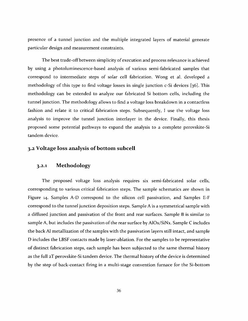
fitting parameter in an optical ray tracing model that fits the sample's absorptance by
varying the reflectivity parameters of the sample. Figure 16 shows the measured reflectance
of each sample for the relevant wavelength range.
0.5
0.45-Sample B
0.4 -Sample C
Sample D- Sample E
0.3 Sample F0.25
0.2 -
0.15 -
0.1
0.05
01000 1020 1040 1060 1080 1100 1120 1140 1160 1180 1200
Wavelength (nm)
Figure 16: Reflectance of the test samples.
Based on the fitted absorptance, the calculated ratio between optical constants is shown in
Table 4. It is possible to observe that the metallized sample C is more reflective than the
calibration sample B. In the same way, the NiOx layer on top seems to make the sample
more reflective compared to sample D.
Table 4: Ratios between absorptance of calibration sample and individual test samples.
Ratio between absorptanceSample
(For calibration samples B and E)
Sample B 1.00
Sample C 1.10
Sample D 1.00
Sample E 1.00
42

Sample F 1.07
The corrected calibration constants for each sample allow to determine the implied Voc as:
Voc = kT * ln(pn/niz) (4)
The pn product is found for each sample and used to calculate the implied Voc. The implied
voltage can be plot as function of the PL illumination intensity in Suns. The two-diode
equivalent circuit equation at the open-circuit could be found from Equation i and is given
by:
IL 01 {exp [ - } -02 {exp ]- 1 (5)
To convert the Suns illumination to current density J, the estimated current density based
on the reference measurements of the J-V device is used. Afterwards, it is possible to fit the
equivalent values of the Jol and Jo2 parameters for each test sample.
3.2.2 Voltage Loss Breakdown
Figure 17 shows the Suns-PL curves for each sample. It is evident that each fabrication
step reduces the voltage for all intensities conditions, shifting the Suns-Vc curve to the left.
A major Voc loss is related to the ITO deposition step. This could be caused by the
sputtering process damaging the front surface of the bottom Si-subcell and increasing the
SRV of the ITO/Si interlayer.
43

-+--Bulk and rear passivation+ Rear contacts
ITO deposition+ NIOx deposition
-+ ITO over a-Si
, 'I.,.
/*,
WI
I,
/
/
/ /9
1.1 -
0.9-
0.8
0.7
C/)
0.6
0.5
0.4
0.6 0.65 0.66 0.67
Figure 17: Suns-PL curve for test samples B-F corresponding to various fabrication steps.
This hypothesis will be investigated later by depositing an amorphous silicon layer
between the Si and ITO layers. Furthermore, it is evident that the cells using spin-coated
layers in the top and bottom subcell have a relative lower voltage loss than cells after
sputtering and metallization.
It is possible to plot the relative voltage loss due to each processing step as a function
of the illumination intensity in Suns, as shown in Figure 18. It is observed that the relative
proportion of the bulk and passivated rear losses are reduced as the illumination intensity
is reduced. Interestingly, the NiOx losses increase as the illumination intensity is reduced.
The device operation as a bottom subcell will limit the spectrum intensity. Thus, as a
representative breakdown for voltage losses an illumination of 0.5 suns will be used.
44
0.61 0.62 0.63 0.64Implied Voc [V]
0.68
I

690 r
680 NiOx lossITO loss
670 ]Rear contacts lossBulk and Passivated rear losses
660
650
640
>630
620-
610
600-
590,
5800.375 0.50 0.625 0.75 0.875 1.00
Suns
Figure 18: Voltage loss breakdown for various illuminations in suns units.
Several uncertainties arise from the methodology. The main ones consists in the
diverse firing and annealing temperature of the samples because of the different heat
transfer samples of different samples. For instance, the metallized samples will likely be
fired at a higher temperature compared to those samples without metallization, due to the
increases thermal conductivity of the sample [541. This could cause discrepancies during
the calibration procedure or the determination of the pn product.
The fitted where J01 and J02 values of each could be subtracted from each other to
find the J0 for each fabrication step. The dark saturation current found for most of the
devices is comparable to the one found for single junction devices [36]. The calculated Jo
for each sample can be normalized against the final J01 of the final sample E. This
normalization provides the relative loss for the whole bottom subcell, including the tunnel
junction. Again, the ITO/Si interlayer is found to be the dominant feature causing voltage
loss.
45

62.68
264.44 UnitsfA/cm2
Figure 19: Jo, voltage loss breakdown for Si bottom cell
3.2-3 Improving the Si/ ITO-interlayer
46
MPassivated emitterBulk and rear passivationRear contactsITO tunnel junction
SNiOx tunnel junctionE Juncton second diode & other

921
83T68 *Units: fA/cm 2
Passivated emitterBulk and rear passivationRear contactsITO tunnel junction
]NiOx tunnel junction=i]iJunction second diode & other
Figure 20: Jo breakdown after deposition of a-Si layer.
It was hypothesized that the significant voltage loss in the ITO/Si interface was
caused by the high surface recombination in the Si layer, which is not adequately passivated
by the ITO. To investigate this hypothesis, an additional passivating layer was deposited
between the n++ emitter of the Si cell and the ITO cell. This additional passivation layer,
commonly used in HIT cells [64], consists of 3 nm of intrinsic a-Si and 20 nm of n+ a-Si.
The intrinsic layer passivates the dangling bond on the surface of the cell before ITO
deposition. The 20 nm n+ a-Si layer preserves the electron conductivity in the ITO
direction. Based on the ITO over a-Si curve, is it observed that the Vc loss is reduced
consistently for all illumination levels, shifting the curve to the right compared to the curve
of the ITO deposition. The final Jo breakdown is shown in Figure 20. The overall voltage
loss is reduced. This exercise proves the usefulness of the proposed methodology to
47

improve the device design, especially in the tunnel junction layers, which are usually
difficult to characterize.
3.2.4 Pathways for perovskite top cell analysis
The voltage loss analysis for the top perovskite device is beyond the scope of this
thesis. However, several ideas are proposed to potentially evaluate the device through the
Suns-PL methodology. On first place, to perform the PC-PL calibration the top subcell has
to satisfy the Plank emission law, which relates de emitted luminesce to the voltage by an
exponential relation. In literature, it has been found that the single junction perovskite
devices satisfy the Planck emission law after been light-soaked. Figure 21, by Hameiri et
al., shows the relation between the emitted PL and the measured voltage at the terminals
of a perovskite device [65].
C
I
104
310
102
.--- 0P 079
PLoce"PL (high to low, correcte in)
A PL (high tolow, ehoected)0 PL (low to high, corected)0 PL (low to high, corected, no light soe'ing)
0.80 0.85
Terminal voltage [VM
0.90
Figure 21: PL counts as a function of terminal voltage for single junction perovskite device.[651.
Figure taken from
48

In consequence, it is possible to measure the PL and obtained calibrated PL maps.
The Suns-PL methodologies must be adapted to analyze the top subcell in the following
ways:
" In the absence of a photoconductance model for perovskite devices, the
perovskite device has to be calibrated by directly contacting the terminal of
the full device under 650 nm illumination. The measured voltage under this
conditions will approximate that of the single subcell.
" An alternative consists in probing the top subcell only by fabricating a 3T
perovskite-Si device. This device, a variation of the 2T device, has a
prominent ITO layer, which allows the probing of the top subcell separately.
49

CHAPTER 4
4 SHUNT IDENTIFICATION INMULTIJUNCTION DEVICES
4.1 Shunts in Multijunction Solar Cells
Shunts are areas of a solar cells that show a dark current contribution additional to the
diffusion current of the cell. Shunts are detrimental to the J-V characteristics and are
originated from material and fabrication quality issues. Two types of shunts are
distinguished: ohmic shunts, which present a linear contribution to the J-V characteristics
and usually dominate under high reverse bias and non-ohmic shunts, which contribute
non-linearly (diode-like) and are most prominent under forward bias. Ohmic shunts are
caused by conduction pathways that short the emitter, while non-ohmic shunts are usually
caused by strongly recombination-active defects crossing the pn junction or by contact
pathways between the metal grid and the base [66]-[68]. Ohmic shunts are more harmful
for solar cell operation and are commonly found during the development of new solar cell
architectures. Ohmic shunts in single junction solar cells are usually known to mainly affect
the fill factor (FF) due to current leakage across the junction, and should be avoided during
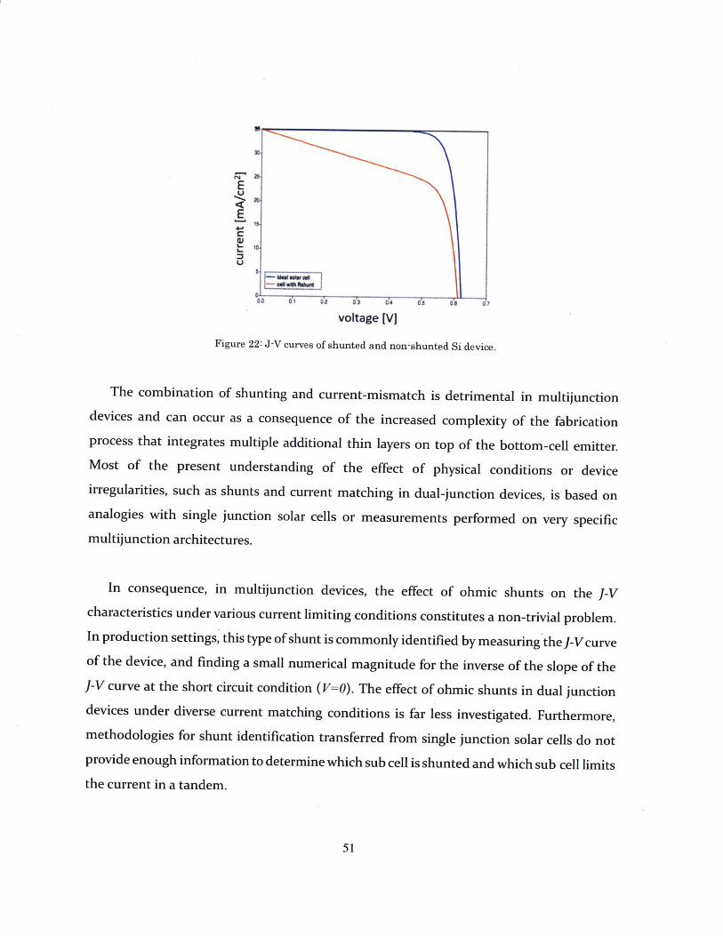
the fabrication process [67]. Figure 22 shows a comparison between a shunted cell and a
non-shunted cell.
50
E
E
U
LII
o7.: o 04 r 0,5 0of 0
voltage [V)
Figure 22: J-V curves of shunted and non-shunted Si device.
The combination of shunting and current-mismatch is detrimental in multijunctiondevices and can occur as a consequence of the increased complexity of the fabricationprocess that integrates multiple additional thin layers on top of the bottom-cell emitter.Most of the present understanding of the effect of physical conditions or deviceirregularities, such as shunts and current matching in dual-junction devices, is based onanalogies with single junction solar cells or measurements performed on very specificmultijunction architectures.
In consequence, in multijunction devices, the effect of ohmic shunts on the J-Vcharacteristics under various current limiting conditions constitutes a non-trivial problem.In production settings, this type of shunt is commonly identified by measuring the J-Vcurveof the device, and finding a small numerical magnitude for the inverse of the slope of theJ-V curve at the short circuit condition (V=0). The effect of ohmic shunts in dual junctiondevices under diverse current matching conditions is far less investigated. Furthermore,methodologies for shunt identification transferred from single junction solar cells do notprovide enough information to determine which sub cell is shunted and which sub cell limitsthe current in a tandem.
51

For instance, previous measurements of 2T GaInAsP/InGaAs tandem devices have found
that, under current mismatch conditions, a non-horizontal slope of the J-V curve close to
the short-circuit conditions have shown to cause the jsc of a device to transition between the
jsc of the current-limiting sub cell to the higher jsc of the non-current limiting sub cell [69].
Further simulation work has determined that this jsc transition occurs in any generic 2T
tandem device [16]. Shunt resistance in multijunction devices has also been found to have
an impact on the coupling current in 2T multijunction devices [70], and spectrometric
characterization has been used to experimentally study shunts under various current
matching conditions [71], [72]. However, previous studies have not systematically
investigated 2T tandem J-V characteristics under a broad range of shunt resistances and
current matching conditions. Furthermore, previous studies have not validated their
conclusions by direct sub cell J-V measurements of 2T tandem solar cells, but by inference
from 2T tandem device J-V curves.
In this context, this part of the thesis analyses numerically and experimentally ohmic
shunts occurring in 2T GaAs/GaAs solar cells for a wide range of current matching
conditions and shunting severity. These results allow to determine several identification
strategies for ohmic shunts in multijunction solar cells in general (including Si-based
multijunction devices), and provides design guidelines to minimize their impact on J-V
characteristics.
4.2 Sentaurus TCAD simulation and equivalent circuit model of 2T
multijunction device
A 20.19% efficient GaAs/GaAs 2T tandem device is modelled based on experimental and
numerical data available in literature [12], [22], [73]. The observed trends are validated in
two ways: 1. by fabricating and directly measuring a modified GaAs/GaAs 2T tandem device
that allows independent proving of each sub cell, and 2. by means of spectrometric
characterization of the device. A Sentaurus TCAD model was used to simulate the device
structure and calculate its optical and electrical characteristics under AM 1.5G illumination.
52

Sentaurus TCAD is a finite element analysis software package for simulation ofsemiconductor devices. The program is able to solve the carrier diffusion equations forsemiconductors for non-trivial 3D geometries and, in the case of optoelectronics problems,couple the equations to optical phenome such as solar cell career generation and radiativerecombination.
A two-dimensional 650 pm symmetry element of the solar cell was modelled,corresponding to the spacing between metal fingers. A GaAs/GaAs tunnel junction,consisting of two lo nm heavily doped GaAs layers (Te dopant, 2Xio' 9 cm-3 and C dopant,
3x1 9. cm-3), was simulated through an interband tunnelling model, accounting for dynamictunnelling [74], [75]. The studied GaAs/GaAs device, including layer thickness and doping,is shown in Figure 23.
Figure 23: 2T GaAs/GaAs tandem device.
The Sentaurus TCAD model allowed to compute the J-V curves of each individualsub cell and the complete tandem stack. The simulated J-V curves for each structure areshown in Figure 24. It is possible to see that in the AM 1.5 G condition, the current limitingsubcell is the bottom subcell. The final voltage of the tandem device corresponds to the sum
53

of the voltage of both subcells.
14- -Top GaAs subcell
Bottom GaAs subcell12 - - -2T GaAs/GaAs tandem
10
E 8-
4
2
010 0.5 1 1.5 2 2.5
V [Voft]
Figure 24: Simulated J-V curves for 2T GaAs/GaAs device.
In order to fit and vary the electric characteristics of each individual sub cell, a full two-diode
equivalent circuit model, as described by Equation 1 in Chapter 3, is used. In this case, Rshunt
is inversely proportional to the severity of the ohmic shunt. Ohmic shunts that affect
significantly the J-V characteristics will be represented by a lower shunt resistance.
54

A- Two mkde Nmdd R-sories
Multijuction Solar Cell Model }2 TrminalTandem
seaw cesTOO CO
Figure 25: Equivalent circuit model for 2T multijunction device.
The resulting subcell parameters obtained by Sentaurus TCAD simulation andsubsequently fitted using Equation 1 are shown in Table 5.
Table 5: Subcell and tandem device characteristics.
GaAs top sub cell
Cell parameter Parameter value
Jai, n=1 4.0625e-21 mA/cm 2
Jo2, n=2 6.669e-14 mA/cm 2
Jsc 13.25 mA/cm 2
VOc 1.091 V
GaAs bottom sub cell
Cell parameter Parameter value
Joi, n=1 8.876-2OmA/cm 2
Jo2, n=2 3.351e-11 mA/cm 2
isc 11.04 mA/cm 2
VOC .0.9907 V
GaAs/GaAs 2T tandem device
Cell parameter Parameter value
Jsc 11.02 mA/cm 2
Vac 2.081 V
55

FF 0.8925
Efficiency 20.19%
The equivalent circuit models for each individual sub cell are connected in series to
simulate a 2T multijunction device, as shown in Figure 25. The double-diode fit of the J-V
curves for individual sub cells defines the equivalent shunt resistance of the circuit, which
approximates the linear J-V contribution of ohmic shunts to the saturation current of the
device. The equivalent shunt resistance for devices with efficiencies similar to the ones
studied in this work are expected to be above io4 K2/cm
2 [16]. Ohmic shunts of increasing
severity can be reasonably modelled by decreasing the equivalent shunt resistance of the
circuit. For the purpose of this study, the following decreasing values of equivalent shunt
resistance are considered: 500, 250, 100, 5o and 1 Q /cm 2 . Furthermore, assuming that the
2T tandem device has a functioning tunnel junction, the sub cell voltages of the top sub cell
Vtop and the bottom sub cell VbOt satisfy the following relation with the tandem voltage [271:
Vtop + VoOt = Vtandem (6)
In order to investigate the effect of shunting under diverse current-mismatch conditions,
three scenarios were considered: i. Currents of top and bottom sub cells are matched. 2. Top
sub cell limits the tandem current and 3. Bottom sub cell limits the tandem current. For each
one of these conditions, the equivalent ohmic shunt resistance of either top or bottom cell
was varied across the stated values.
4-3 J-V curves under various current matching and shuntingconditions
Figure 26 and Figure 27 show the calculated J-V curves of the tandem device under
different scenarios of current-limiting and shunting conditions. Figure 26 considers
moderate current mismatch (-io% relative), a common current mismatch magnitude for III-
56

V multijunction devices [12], while Figure 27 considers severe current mismatch (>50%relative). For both cases, the observed trends differ significantly from the well-known trends
of shunted single junction devices. In general, it is observed that FF, V, and Jsc are affected
as the shunt resistance diminishes. However, in contrast with single junction devices, it isobserved that the current mismatch conditions have a determinant effect on how severe the
FF, Voc and Js, affectations are.
TOP CELL SHUNTED BOTTOM CELL SHUNTED
a)
0.5 1 1.5 2 2.V [Volt]
ONSET VOLTAGE b)-- Baseline
-- 500 Q250 Q
-- 100 Q-so n -_1 i
2
5
2.5
c)
14,12
E 108 -
S64-2
0
14 -12
E 10-8
E 64.2
0
EE
W C
Oa,
- E
O E
Z E,
- ,E
141210
8-64.2
0
d)- Baseline- 5000
250 i-10010- 50R-1 Q
0.5 1 1.5V [Volt]
2 2.5
e)- Baseline- 500 0
2500- 100 Q
-50-10i
0.5
- Baseline-500 0
250 0- 100 0
50Q- it
0.5
1 1.5V [Volt]
2 2.5
~cj~1 1.5
V [Volt)
Figure 26: J-V curves for different shunting and current limitation conditions. A moderate current mismatchbetween subcells is assumed.
57
-Baseline- 5000
250 1-- 100 Q
-50 0-1 01
141210
8642
1412108642
1 1.5 2 2.5V [Volt]
0 0.5 1 1.5V [Volt]
1412108642
- Baseline- 5000
250 it-- 100 0-50 1
0 0.5
f)
2 2.5
-
.
-

TOP CELL SHUNTED BOTTOM CELL SHUNTED
0. 2 a) -Baseline 14 - - BaselineO ,n 1- -- 500 QI-E 10 250n 10- 250 08 - 1000 8 - 100 i6 500 6 - 500-4 4, -1\
2 2
0 0.5 1 1.5 2 2.5 3 0 0.5 1 1.5 2 2.5 3V [Volt] V [Volt]
14 -- Baseline 12 d) - Baseline01 0 12--500 0o . E 10 250 00 o - - 100a 8 - 1000Q Z6 -- 0 E 6 -- 501)
Z E4o 4 - ~ -102 2
0 0.5 1 1.5 2 2.5 3 0 0.5 1 1.5 2 2.5 3V [Volt] V [Volt]
Figure 27: J-V characteristics for various shunting and current limitation conditions. Severe mismatch betweensubcells is supposed.
As the equivalent shunt resistance decreases, it is observed that the open-circuit
voltage (Voc) of the tandem device approaches the V, of the non-shunted sub cell for all
current-limiting cases. For very low shunt resistance and shunting of the
non-current-limiting cell in figures 26c and 26e, the J-V curve of the tandem solar cell and
the non-shunted cell are equal. As a consequence of this trend, the calculated J-V curves
tend to distort around a common point as the shunting in a current-limiting cell increases,
which we could refer to as the onset voltage. For Figure 26 and Figure 27, it is observed that
the onset voltage tends to be between the open-circuit voltage (V.,) and the maximum power
point voltage (Vmpp) of the non-shunted sub cell. In consequence, when the sub cells in a 2T
series-connected tandem device have very different V0 c's and present severe shunting, either
the onset voltage or the shape of the device J-V being similar to the sub cell J-V curve may
allow to identify the shunted sub cell.
Comparing Figure 26b and Figure 26c, it is evident that the FF is more significantly
affected when the shunting occurs in the current-limiting cell, compared to the non-
current-limiting cell. In this context, Figure 28 illustrates the impact of progressive shunting
58

over the fill factor for different sub cells under moderate current mismatch. Based on Figure
27, it is also evident that severe current mismatch conditions increase the magnitude bywhich the FF is affected by shunting in current-limiting sub cells. Furthermore, a
comparison of Figure 26 and Figure 27 allows to conclude that the V, and FF of the device
are more significantly affected by shunting when the current mismatch is severe. This
conclusion emphasizes the importance of current matching for reducing the severity of
ohmic shunts in 2T dual junction devices. Adequate current matching of 2T tandem devices
could be realized by choosing adequate thicknesses for top and bottom sub cells or tuning
the top cell band gap appropriately [231.
Shunt in Current Limiting Cell-Shunt in Non-Current Limiting Cell
0.90S0.8 -
ccLL
E 0.7
0.6)
04
0.5
101 100 101 102
Shunt Resistance [D]
Figure 28: Fill factor of the 2T tandem device as a function of shunt resistance.
For current-matched conditions, as shown in Figure 26a and Figure 26d, J-V curves
are distorted as the shunt resistance decreases. The observed distortion reduces both the FF
and the V, of the device, but the Js, remains constant for each shunting scenario. For
moderate current mismatch conditions, Figure 26c and Figure 26f illustrate that, when the
non-current-limiting sub cell is shunted, the J-V curves for decreasing values of shunt
resistance are very similar to the case when both cells are current-matched. In this case, the
59

jsc of the device corresponds to the jsc of the current-limiting cell, or is very close to it. In
contrast, as shown in Figure 26b and Figure 26e, as the current-limiting sub cell is
increasingly shunted, the dual junction device jsc transitions from the jsc of the current-
liming sub cell to the jsc of the non-current-limiting sub cell. The same trend is evident for
severe current mismatch conditions in Figure 27a and Figure 27d.
The effect of the non-zero slope close to jsc in the sub cell's J-V curve explains the
observed jsc transition. We know that for short-circuit conditions the voltages of both
sub cells connected by a working tunnel junction, Vt, and Vbt, should follow Vtp + V,,t =
0 [16]. If the slope of the shunted cell close to its jsc is non-horizontal, the cell will operate in
reverse bias. In that case, equations 5 and 6 can only be satisfied by a jsc that is higher than
the jsc of the current-limiting cell, explaining the current transition. In the context of the
equivalent circuit representation of the tandem device, this trend could be interpreted as
the reduced shunt resistance electrically isolating the rectifying characteristics of the
current-limiting cell and, consequently, reducing its limiting effect over the whole tandem
device. Arguably, knowledge of the js, transition could be used to identify the shunted
sub cell in a tandem architecture. If the current-limiting sub cell is known, the occurrence
of the jsc transition will suggest the existence of an ohmic shunt in the current-limiting
subcell.
4.4 Experimental validation
4.4.1 Measurement of 3T device
Finally, to verify the J-V trends found through simulation, we fabricated, shunted and
directly measured the J-V curves of a modified 1 cm 2 GaAs/GaAs dual junction solar cell [231.The GaAs/GaAs cell was fabricated on epi-ready <ioo> oriented GaAs on-axis wafers using
an MOCVD reactor, and is identical to the simulated device shown in figure 1. The MOCVD
growth was performed under a pressure of ioo mbar using TMGa, TMIn, AsH 3 and PH 3 as
60

precursors and H2 as carrier gas. Prior to the laser isolation of the 1 cm2 area, the heavily
doped GaAs layers of the 20 nm tunnel junction extended beyond the device area, acting as
an intermediate contact that allows the measurement of each sub cell independently [76],
[77]. It is important to note that this cell, and its measured sub cells characteristics, are not
equal to the simulated 20.19% efficient GaAs/GaAs 2T tandem, because of the presence of
the intermediate contact [76].
The GaAs/GaAs device was shunted by scribing the front of the device with a diamond
scriber, a common method for on purpose creation of ohmic shunts in III-V and Si devices
[67], [78]. However, due to the small thickness of the top sub cell, it was not possible to shunt
each GaAs sub cell independently and both sub cells showed a decreased ohmic shunt
resistance after the scribing process. Finally, the J-V curve of each sub cell and the whole
device were measured under AM1. 5G spectrum.
The trends obtained from simulation were validated experimentally by measuring the
J-V curves of each sub cell of the fabricated GaAs/GaAs device. This cell, in contrast with
the 20.16% GaAs/GaAs cell simulated in Sentaurus TCAD, includes an intermediate contact.
Figure 29 shows the J-V curves of the device and each of its sub cells after they are shunted.
The resulting sub cell curves where used as fitting datasets for the equivalent circuit model,
and a theoretical J-V curve was calculated. The observed trends are consistent with
modelling and literature results [16], [791. It is evident that the fabricated non-shunted 2T
GaAs/GaAs cell is similar to the simulated GaAs/GaAs cell, shown in figure 2. The higher jsc
of the fabricated 2T GaAs/GaAs device compared to the simulated device (13-38 mA/cm 2
compared to 11.04 mA/cm2) is explained due to the fact that the top sub cell constitutes the
current limiting sub cell for the case of the fabricated sample. This relative higher jsc of the
bottom sub cell is caused by the non-isolated area of the bottom cell, which allows to include
the intermediate contact in the device, but also contributes with additional parasitic current
to the sub cell jsc. In similar way, the discrepancy between the jsc of the shunted top sub cell
and the jsc of the non-shunted 2T GaAs/GaAs cell could be explained by parasitic currents
61
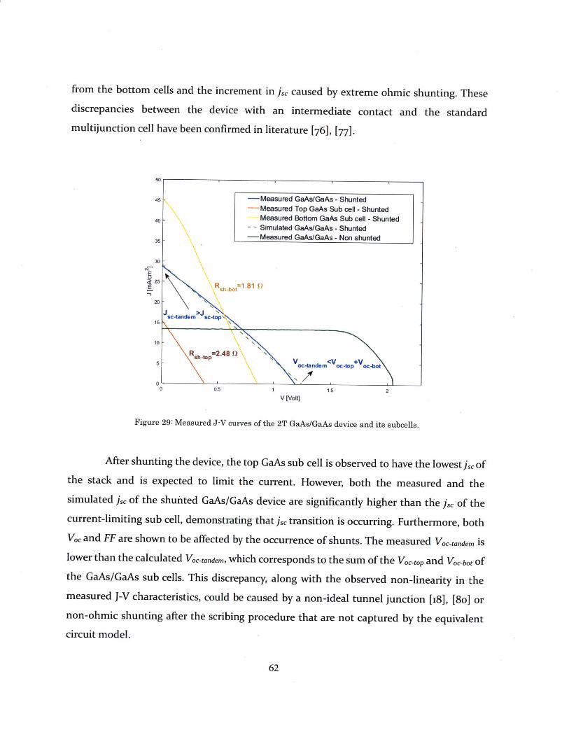
from the bottom cells and the increment in jsc caused by extreme ohmic shunting. Thesediscrepancies between the device with an intermediate contact and the standardmultijunction cell have been confirmed in literature [76], [77].
s
45
40
35
30
E25
20
I5
10
5
00 0.5 1.5 2
V [Volt]
Figure 29: Measured J-V curves of the 2T GaAs/GaAs device and its subcells.
After shunting the device, the top GaAs sub cell is observed to have the lowest js of
the stack and is expected to limit the current. However, both the measured and the
simulated js, of the shunted GaAs/GaAs device are significantly higher than the jsc of the
current-limiting sub cell, demonstrating that js transition is occurring. Furthermore, bothV, and FF are shown to be affected by the occurrence of shunts. The measured Voc-tandem islower than the calculated Voc-tandem, which corresponds to the sum of the Vc-t0p and Voc-bot of
the GaAs/GaAs sub cells. This discrepancy, along with the observed non-linearity in the
measured J-V characteristics, could be caused by a non-ideal tunnel junction [18], [8o] ornon-ohmic shunting after the scribing procedure that are not captured by the equivalent
circuit model.
62
-Measured GaAs/GaAs - ShuntedMeasured Top GaAs Sub cell - ShuntedMeasured Bottom GaAs Sub cell - Shunted
- - Simulated GaAs/GaAs - Shunted-Measured GaAs/GaAs- Non shunted
R h-bt=l1.81S?
-
-N
R 2.48 Q
c-tandem sop +

Several factors beyond the simulation and experimental limitations could affect the
observed J-V curve trends. For the simulated II-V tandem device, the reabsorption of
radiatively recombined photons, or photon recycling, will likely improve the fill factor and
reduce the relative severity of shunting [22], [81]. Furthermore, the presence of shunts with
non-ohmic characteristics [67], [82] or the non-negligible series resistance in the device
could affect the shape of the J-V curves in dissimilar ways [68], [83].
4-4.2 Spectrometric characterization
Conventionally, in order to maximize the power output of the device, the individual
currents of the subcells under standard AM1. 5G illumination conditions are matched by
adjusting the thicknesses or band gaps of the subcells. Nevertheless, spectral variations
during solar cell operation could affect significantly the currents and J-V characteristics of
the subcells. If one of the subcells has a shunt, the maximum power output of the device
might not correspond to the current-matched case due to changes in the J-V characteristics
of the device. Furthermore, a J-V measurement under standard AMi. 5 G laboratory
conditions may not reveal the presence of shunts which affect the device efficiency under
real operating conditions.
Spectrometric characterization is a common technique used to study the subcell J-V
parameters [72]. The technique consists in systematically varying the spectral distribution
of the illumination over a multijunction solar cell. For a 2T multijunction device, given that
the blue part of the spectrum is mainly absorbed by the top sub cell and the infrared part
of the spectrum is absorbed by the bottom sub cell, the spectral variations cause different
current matching conditions, and allows to analyze each subcell quasi-independently,
optimize current-matching conditions and determine spectrum-induced voltage shifting.
Spectrometric characterization has been performed before, with various degrees of
accuracy, employing filters in a single-source solar simulator or Xenon lamp, or using LED
solar simulators [72].
63

In this section, spectrometric characterization is used to identify the shunted subcell in a
monolithic GaAs/GaAs device, and quantify the shunt effects under various current
limitation conditions. The resulting J-V curves are fitted through an equivalent-circuit
model with the aim of interpreting the observed effects over J-V characteristics. This
methodology allows the identification and characterization of shunts in multijunction
devices for a wide range of operating conditions. We study the same 2T GaAs/GaAs device
architecture used in the previous section. However, this time we use a test device with an
efficiency, without an antireflective coating, of 13.9%. A priori, the device is believed to be
shunted, but the actual location and shunt characteristics are unknown.
The spectrometric characterization procedure was performed with a Wavelabs, Sinus-22o
LED-based I-V tester. The tester is comprised of 21 LEDs of different wavelengths that allow
approximating the distribution of any arbitrary solar spectrum. The average photon energy
(APE), which represents the average energy per photon in a given spectrum, is used as a
proxy for spectrum shape. A higher APE value corresponds to a blue-rich spectrum and, in
consequence, a higher photogenerated current in the top GaAs subcell. In the same way, a
lower APE value corresponds to spectral distribution shifted to the infrared. For this study,
APE values in the range of 1.70 eV - 1.95 eV were approximated, corresponding to real
spectra measured in Singapore. To avoid variations in irradiance level, all the spectra were
scaled to match the power of the AMi. 5G spectrum in the 300-noo nm wavelength range.
Figure 30 shows the LED-approximated spectra with different APE values.
64

E
CN
E
a,
:5
3.5 -T
Average Photon Energy (APE) [eV]
3 -1.83 (AM1.5G) -1.71 -1.75 1.79 -1.95
2.5-
2
1.5
0.5
0300 400 500 600 700 800 900 1000 1100 1
Wavelenght [nm]00
Figure 30: LED spectra of the equal irradiance level and different APE values, approximating real spectrameasured in Singapore.
The J-V characteristics of the multijunction device were measured for eachspectrum. To analyze the observed trends, the equivalent-circuit model used in theprevious section is employed. The standard double-diode equation was modified toaccount for photoluminescence and electroluminescence coupling [23].
The dark saturation current and the short-circuit current density (j,) of each subcellare required for the model. The input parameters were found by fitting the J-Vcharacteristics of the device under AMi. 5G illumination (APE 1.83 eV) using the SentaurusTCAD model. The calculated input parameters for the equivalent-circuit model are shownin Table 6.
65
_

Table 6: Input parameters and characteristics of GaAs/GaAs device at standard conditions (AM 1.5G).
GaAs top subcell
Cell parameter Parameter value
Joi, n=i 1.36-17 mA/cm 2
J02, n=2 i.ne-ii mA/cm 2
Jsc 8.98 mA/cm 2
Voc 1.028 V
GaAs bottom subcell
Cell parameter Parameter value
Joi, n=i 8.48-17mA/cm 2
J02, n=2 1.33e-1 mA/cm 2
Jsc 8.82 mA/cm 2
Voc o.994 V
GaAs/GaAs monolithic tandem device
Cell parameter Parameter value
Jsc 8.82 mA/cm2
Voc 2.022 V
FF o.8425
Efficiency 13.9%
The GaAs/GaAs tandem cell was measured under the specified spectrum conditions at
constant intensity. The measured J-V curves are show in Figure 31. The jsc of the tandem
device and the cell acting as the current-limiting subcell change as the spectrum is shifted.
For APE values over the AM 1-5G condition (1.83 eV), the jsc of the tandem device is reduced
as the bottom cell is depleted of light. For APE values over the AM 1.5 G condition, a higher
66
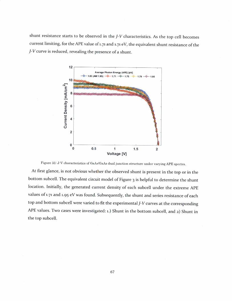
shunt resistance starts to be observed in the J-V characteristics. As the top cell becomes
current limiting, for the APE value of 1.71 and 1.71 eV, the equivalent shunt resistance of theJ-V curve is reduced, revealing the presence of a shunt.
12
4.'
(n
Average Photon Energy (APE) [eV]
-- 1.83 (AM 1.5G) -- 1.71 -4-1.75 C 9 1.79 --0- 1.95
0<-
8
6
4-
2
U-0 0.5 I
Voltage [V]1.5 2
Figure 31: J-V characteristics of GaAs/GaAs dual junction structure under varying APE spectra.
At first glance, is not obvious whether the observed shunt is present in the top or in thebottom subcell. The equivalent circuit model of Figure 3 is helpful to determine the shunt
location. Initially, the generated current density of each subcell under the extreme APEvalues of 1.71 and 1.95 eV was found. Subsequently, the shunt and series resistance of each
top and bottom subcell were varied to fit the experimental J-V curves at the corresponding
APE values. Two cases were investigated: i.) Shunt in the bottom subcell, and 2) Shunt in
the top subcell.
67
1

10
9
E
6
0 5APE [eV]
C 4 --- 1.71 - Measured- 1.71 - Sim. Top cell shunted
3 3 1.71 - Sim. Bottom cell shunted- - - 1.95 - Measured- 1.95 - Sim. Top cell shunted
2 1.95 - Sim Bottom cell shunted
10 0.5 1 1.5 2
Voltage [V]
Figure 32: Measured and simulated J-V curves of cell at APE values of 1.71 and 1.95 eV
Figure 32 compares the measured and simulated J-V curves at the two APE values.
Both simulated curves of top and bottom shunted cell have the same equivalent shunt
resistance. It is possible to identify the shunted cell as the top cell, because it approximates
with good agreement the measured J-V curves. For the 1.71 eV APE condition, the top cell
is the current-limiting cell. However, the final jsc of the simulated cell varies according to
which subcell is shunted. In the case in which the shunt is occurring in the current-limiting
cell, the jse of the tandem device is observed to be higher than that js, of the current-limiting
subcell. The effect of the non-zero slope close to the shunted subcell's jsc explains the
observed jsc transition. We know that for short-circuit conditions the voltages of both
subcells connected by a working tunnel junction, Vtop and VbOt, are subjected to Vtop +
Vbot = 0. If the slope of the shunted subcell close to its jsc is non-horizontal, the cell will
operate in reverse bias. In that case, the diode equation can only be satisfied by a js that is
higher than the jsc of the current-limiting cell, explaining the current transition. In the
context of the equivalent circuit representation of the tandem device, this trend could be
interpreted as the reduced shunt resistance electrically isolating the rectifying
68

characteristics of the current-limiting cell and, consequently, reducing its limiting effect
over the whole tandem device. Consistently, this effect is not observed in the case of the
shunting in the bottom subcell, which is the non-limiting subcell for lower APE values. In
the opposite case, for the 1.95 APE value condition, the bottom subcell acts as the current-
limiting subcell. In this scenario, the shunt in the top subcell fits adequately the measured
data, because the measured jsc of the device does not surpass the jsc of the current-limiting
subcell.
69

CHAPTER 5
5 CONCLUSIONSPerovskite-Si tandem solar cells have the potential to boost the efficiency of commercial
single Si technologies in a cost-effective manner. In this thesis, I developed a framework for
producing low cost Si cells that can be operated in a two-terminal tandem configuration
with a perovskite top subcell. The framework was composed of the following fabrication and
characterization aspects: Si bottom subcell fabrication, voltage loss analysis and shunt
identification.
The perovskite-Si cell framework is expected give important tools for future fabrication
of 2T high-efficiency, low-capex devices perovskite-Si solar cells. The fabricated structure
could be readily and adapted and optimized for future low-capex architectures, whereas the
characterization procedures could be used for a fast and accurate determination of voltage
and shunting losses in almost all types of Si-based 2T tandem device. The conclusions and
future work are broken down for each aspect of the proposed framework and are commented
in the following sections.
BOTTOM SI CELL FABRICATION
To allow the deposition of the top perovskite subcell and fabricate a cost-effective, high
efficiency two-terminal tandem, the following device requirements for the Si bottom subcell
were defined: mirror-like front polished surface, high single junction efficiency (comparable
to commercial single junction Si cells), no oxide layers and highly uniform front surface, low
70

production cost and capital expenditure. In this context, two low-capex p-type bottom Si
architectures that could satisfy these requirements were fabricated and measured: BSF and
LBSF solar cells. Due to its higher efficiency and little additional cost compared to the BSF
architecture, the LBSF cell was chosen as a suitable cell for a perovskite-Si device.
A batch of LBSF bottom Si subcells was fabricated with a single junction reference
efficiency of 16.8% under AM 1.5G spectrum. These cells were adapted for bottom subcell
operation by 1) using a polished front surface wafer, 2) optimizing the firing and
back-contact deposition, 3) establishing adequate cleaning and oxide etching procedures
before tunnel junction deposition, 4) defining an effective and easy-to-remove masking
stack to protect the cells in intermediate steps and reducing the voltage loss in the ITO/Si
interlayer.
First, the sourced single-side polished Cz wafers were analysed and validated for
adequate lifetimes (300-800 ps). Subsequently, the quality of the dopant diffusion into the
planar surface was tested. The test wafers with diffused junction were found to have an
average lifetime of 150 [s, which is an acceptable lifetime figure for Cz wafers with diffused
junctions [40]. The baseline firing temperature profile for the LBSF bottom Si subcell was
determined by measuring fully metallized reference cells under different firing
temperatures. The highest efficiency was achieved for a firing temperature profile in multi-
stage furnace of 740-710-210 'C. Future work should consider various texture qualities in
addition to firing profiles. A HF etching and solvent cleaning process was developed to
preserve the Si front surface quality before ITO deposition and avoid pinholes in the
perovskite top cell. Additionally, appropriate masking and texturing steps were defining by
identifying the process that yield the highest reference efficiency and are compatible with
the perovskite deposition steps.
The process modification allows to get a bottom subcell Si device with an adequate
efficiency baseline for ongoing perovskite-Si integration. The final efficiencies of the
71

two-terminal perovskite-Si device will be reported in incoming publications. Further work
in this area should aim to optimize the red response of the device and, consequently, increase
the Js, of the bottom subcell. Similar work has been performed for n-type HIT bottom
subcells to reach record efficiencies [24].
VOLTAGE LOSS ANALYSIS OF BOTTOM SI SUBCELL
Based on the established methodology for finding an open-circuit voltage breakdown in
LBSF devices, a voltage loss analysis methodology was developed to characterize the bottom
Si subcell and the tunnel junction. The methodology is based in contactless QSS-PC and PL
measurements of semi-fabricated structures. The voltage of the structures without
metallization is measured by QSS-PC, and used for a self-consistent calibration procedure
of the metalized samples. In contrast with other voltage loss analysis methodologies, this
experimental setup allows to obtain the voltage loss of various critical processing steps with
high detail without the need of complex computational models.
Applied to LBSF bottom Si subcell, the voltage loss analysis provides a loss breakdown of
the main voltage loss mechanics as a function of the Vc and the recombination current Jo of
the device. The ITO deposition step was identified as producing the greatest voltage loss,
with a Jo contribution of 264.67 fA/cm2. This loss was likely caused by the sputtering
procedure affecting the Si front surface, and the scarce surface passivation provided by the
ITO layer. To reduce this loss, an a-Si stack was deposited between the Si surface and the
ITO layer to reduce the recombination losses. The a-Si stack was found to reduce the voltage
losses significantly, and the new measured Jo was 44.64 fA/cm2. The additional lost
mechanisms were found to be have similar contribution as in the case of single junction
device, as expected. A relatively high loss contribution of the spin-coated NiOx layer was
found, which was unexplained by the spin coating process. Future work should try to
72

identify likely causes of this NiOx loss.
I suggested various pathways for expanding the analysis to the top perovskite subcell.
The main challenge for performing calibrated PL measurement of perovskite devices is the
difficulty of measuring the excess carrier density or Vc of intermediate structures in the 2T
tandem device. In this scenario, several option were suggested: i) probing a 3T multijunction
device to find the Vc of the top perovskite subcell for various illumination intensities, 2)
exciting the perovskite junction and measuring the Vc of the whole tandem, subtracting any
parasitic PL emission. Furthermore, future work should focus in finding suitable interlayers
between ITO, or other similar tunnelling layer such as IZO, and the Si emitter. The voltage
loss analysis could be extended to the complete device stack, allowing the optimization of
other material layers in the perovskite subcell and the evaluation of the impact of the Si
surface on the efficiency of the 2T device.
SHUNT IDENTIFICATION IN MULTIJUNCTION DEVICES:
Ohmic shunts in 2T series-connected tandem solar cells are affected by multiple factors
that commonly do not influence single junction devices. This work provides a systematic
analysis of the effects of ohmic shunts on J-V characteristics for several shunting severities
and current mismatch conditions among sub cells. Simulating the performance of a
GaAs/GaAs dual-junction solar cell allows to determine the effect of shunting on the J-V
characteristics for moderate and severe current mismatch conditions. Three main trends
were observed: i.) Ohmic shunts in 2T tandem devices affect FF, jsc and Vc. For increasing
shunt severity, the onset voltage of the devices approaches the V, of the non-current-
limiting sub cell. 2.) The FF is more significantly affected when the ohmic shunts occur in
the current-limiting sub cell of the tandem device, with an up to 20% different between the
FF figures. 3.) The severity of the current mismatch between sub cells determines the
severity of the effects of shunting on V0, and FF. 4.) The jsc of the tandem device transitions
from that of the current-limiting sub cell to that of the non-current-limiting sub cell, as the
73
current-limiting cell is shunted. The jsc transition is caused by the non-horizontal slope of
the current-limiting sub cell close to itsjsc point. Thejs was found to change as much as 50%
when the device is shunted, depending on the initial current mismatch.
The observed trends were validated by fabricating and measuring a modified 2T
GaAs/GaAs device in which the individual sub cells were proven independently. The
simulated J-V curves of the tandem device showed good agreement with the measurements.
The discrepancy of the curves were attributed to contribution of non-ohmic shunts, parasitic
currents and a non-ideal tunnel junction. The results allow characterizing ohmic shunts and
identifying current-limiting sub cells in multijunction devices. Furthermore, the results
allow to design 2T dual-junction devices in a way in which shunt effects are minimized.
Future work should take into account the effects of non-ohmic shunts, high series resistance
and photon recycling.
A new methodology for identifying the shunted subcell and the shunt characteristics
under varying spectrum conditions in a monolithic multijunction devices was developed.
Spectrometric characterization was used to measure the J-V characteristics of a GaAs/GaAs
device under various current-limiting conditions. By using an equivalent circuit model, the
shunted subcell was identified and the observed J-V characteristics were explained. This
method can be transferred to any monolithic multijunction device and could be used in
the development process of the new multijunction architectures, such as perovskite-Si
tandem devices.
74

References
[i] J. Rogelj, M. Den Elzen, T. Fransen, H. Fekete, H. Winkler, R. Schaeffer, F. Sha, K.Riahi, and M. Meinshausen, "Perspective : Paris Agreement climate proposals needboost to keep warming well below 2 C," Nat. Clim. Chang., vol. 534, no. June, pp.631-639, 2016.
[21 G. P. Peters, R. M. Andrew, J. G. Canadell, S. Fuss, R. B. Jackson, J. I. Korsbakken, C.Le Quere, and N. Nakicenovic, "Key indicators to track current progress and futureambition of the Paris Agreement," Nat. Clim. Chang., vol. 7, no. n8, 2017.
[3] D. B. Needleman, J. R. Poindexter, R. C. Kurchin, I. M. Peters, G. Wilson, and T.Buonassisi, "Economically Sustainable Scaling of Photovoltaics to Meet ClimateTargets," Energy Environ. Sci., vol. 9, pp. 2122-2129, 2016.
[4] D. M. Powell, M. T. Winkler, A. Goodrich, and T. Buonassisi, "Modeling the costand minimum sustainable price of crystalline silicon photovoltaic manufacturing inthe united states," IEEEJ. Photovoltaics, vol. 3, no. 2, pp. 662-668, 2013.
[5] D. M. Powell, M. T. Winkler, H. J. Choi, C. B. Simmons, D. B. Needleman, and T.Buonassisi, "Crystalline silicon photovoltaics: a cost analysis framework fordetermining technology pathways to reach baseload electricity costs," EnergyEnviron. Sci., vol. 5, no. 3, p. 5874, 2012.
[6] J. P. Mailoa, C. D. Bailie, E. C. Johlin, E. T. Hoke, A. J. Akey, W. H. Nguyen, M. D.McGehee, and T. Buonassisi, "A 2-terminal perovskite/silicon multijunction solarcell enabled by a silicon tunnel junction," Appl. Phys. Lett., vol. io6, no. 12, p. 121105,2015.
[7] T. Kirchartz and U. Rau, "Detailed balance and reciprocity in solar cells," Phys.Status Solidi Appl. Mater. Sci., vol. 205, no. 12, pp. 2737-2751, 2008.
[8] W. Shockley and H. J. Queisser, "Detailed balance limit of efficiency of p-n junctionsolar cells," J. Appl. Phys., vol. 32, no. 3, pp. 510-519, 1961.
[9] V. D'Innocenzo, A. R. Srimath Kandada, M. De Bastiani, M. Gandini, and A.Petrozza, "Tuning the light emission properties by band gap engineering in hybridlead-halide perovskite.,"J. Am. Chem. Soc., vol. 136, no. 51, pp. 17730-17733, 2014.
[io] S. Rifhle, "Tabulated values of the Shockley-Queisser limit for single junction solarcells," Sol. Energy, vol. 130, pp. 139-147, 2016.
[n] A. International, ASTM Standard G173, Standard Tables for Reference Solar SpectralIrradiances: Direct Normal and Hemispherical on 370 Tilted Surface. WestConshohocken, PA.
75

[12] H. Cotal, C. Fetzer, J. Boisvert, G. Kinsey, R. King, P. Hebert, H. Yoon, and N.Karam, "Ill-V multijunction solar cells for concentrating photovoltaics," EnergyEnviron. Sci., vol. 2, no. 2, p. 174, 2009.
[13] A. De Vos, "Detailed balance limit of the efficiency of tandem solar cells," vol. 839.
[14] P. Baruch, A. De Vos, P. T. Landsberg, J. E. Parrott, and U. Gent, "On somethermodynamic aspects of photovoltaic solar energy conversion a ,*," Sol. EnergyMater. Sol. Cells, vol. 36, no. 2, pp. 201-222, 1995.
[15] C. D. Bailie, M. G. Christoforo, J. P. Mailoa, A. R. Bowring, E. L. Unger, W. H.Nguyen, J. Burschka, N. Pellet, J. Z. Lee, M. Gritzel, R. Noufi, T. Buonassisi, A.Salleo, and M. D. McGehee, "Semi-transparent perovskite solar cells for tandemswith silicon and CIGS," Energy Environ. Sci., vol. 8, no. May 2016, pp. 956-963, 2014.
[16] X. Liao, X. Xiang, and X. Zeng, "Modeling analyses for current matching in tandemsolar cells," IEEE Int. Conf Electro Inf Technol., pp. 0-3, 2013.
[17] M. Yamaguchi, T. Takamoto, K. Araki, and N. Ekins-Daukes, "Multi-junction III-Vsolar cells: Current status and future potential," Sol. Energy, vol. 79, no. i, pp. 78-85,2005.
[18] J. M. 0. Zide, A. Kleiman-Shwarsctein, N. C. Strandwitz, J. D. Zimmerman, T.Steenblock-Smith, A. C. Gossard, A. Forman, A. Ivanovskaya, and G. D. Stucky,"Increased efficiency in multijunction solar cells through the incorporation ofsemimetallic ErAs nanoparticles into the tunnel junction," Appl. Phys. Lett., vol. 88,no. 16, 2006.
[19] H. Liu, Z. Ren, Z. Liu, A. G. Aberle, T. Buonassisi, and I. M. Peters, "The realisticenergy yield potential of GaAs-on-Si tandem solar cells: a theoretical case study,"Opt. Express, vol. 23, no. 7, p. A382, 2015.
[20] M. Jaysankar, W. Qiu, M. van Eerden, T. Aernouts, R. Gehlhaar, M. Debucquoy, U.W. Paetzold, and J. Poortmans, "Four-Terminal Perovskite/Silicon MultijunctionSolar Modules," Adv. Energy Mater., vol. 1602807, p. 1602807, 2017.
[21] T. Kirchartz, U. Rau, M. Hermle, A. W. Bett, A. Helbig, and J. H. Werner, "Internalvoltages in Galn/PGaInAs/Ge multijunction solar cells determined byelectroluminescence measurements," Appl. Phys. Lett., vol. 92, no. 12, 2008.
[22] Z. Ren, J. P. Mailoa, Z. Liu, H. Liu, S. C. Siah, T. Buonassisi, and I. M. Peters,"Numerical Analysis of Radiative Recombination and Reabsorption in GaAs/SiTandem," IEEE J. Photovoltaics, vol. 5, no. 4, pp. 1079-1086, 2015.
[23] Z. Ren, H. Liu, Z. Liu, C. S. Tan, A. G. Aberle, T. Buonassisi, and I. M. Peters, "TheGaAs/GaAs/Si solar cell ??? Towards current matching in an integrated twoterminal tandem," Sol. Energy Mater. Sol. Cells, vol. 16o, no. August 2016, pp. 94-100, 2017.
76
[24] K. A. Bush, A. F. Palmstrom, Z. (Jason) Yu, M. Boccard, R. Cheacharoen, J. P.Mailoa, D. P. McMeekin, R. L. Z. Hoye, C. D. Bailie, T. Leijtens, I. M. Peters, M. C.Minichetti, N. Rolston, R. Prasanna, S. E. Sofia, D. Harwood, W. Ma, F. Moghadam,H. J. Snaith, T. Buonassisi, Z. C. Holman, S. F. Bent, and M. D. McGehee, "23.6%-Efficient Monolithic Perovskite/Silicon Tandem Solar Cells with ImprovedStability," Nat. Energy (under Rev., vol. 17009, no. February, pp. 1-7, 2017.
[25] W. W. and E. D. D. Martin A. Greenl*, Keith Emery2, Yoshihiro Hishikawa3, "SolarCells Efficiency Tables," Prog. Photovolt Res. Appl., vol. 15, no. February 2013, pp-659-676, 2014.
[26] T. Takamoto, M. Yumaguchi, E. Ikeda, T. Agui, H. Kurita, and M. Al-Jassim,"Mechanism of Zn and Si diffusion from a highly doped tunnel junction forInGaP/GaAs tandem solar cells," J. Appl. Phys., vol. 85, no. 3, pp. 1481-1486, 1999.
[27] D. J. F. and S. K. J. M. Olson, High-Efficiency III-V Multijunction Solar Cells. JohnWiley & Sons, 2012.
[28] H. Taguchi, T. Soga, and T. Jimbo, "Fabrication of GaAs/Si tandem solar cell byepitaxial lift-off technique," Japanese J. Appl. Physics, Part 2 Lett., vol. 42, no. 12 A,2003.
[29] K. Derendorf, S. Essig, E. Oliva, V. Klinger, T. Roesener, S. P. Philipps, J. Benick, M.Hermle, M. Schachtner, G. Siefer, W. Jdger, and F. Dimroth, "Fabrication ofGaInP/GaAs//Si solar cells by surface activated direct wafer bonding," IEEEJ.Photovoltaics, vol. 3, no. 4, pp. 1423-1428, 2013.
[30] J. Werner, L. Barraud, A. Walter, M. Bruninger, F. Sahli, D. Sacchetto, N. Tetreault,B. Paviet-Salomon, S.-J. Moon, C. Allebe, M. Despeisse, S. Nicolay, S. De Wolf, B.Niesen, and C. Ballif, "E ffi cient Near-Infrared-Transparent Perovskite Solar CellsEnabling Direct Comparison of 4 - Terminal and Monolithic Perovskite/SiliconTandem Cells," ACS energy Lett., vol. 1, p. 474-480, 2016.
[31] J. H. Heo, H. J. Han, D. Kim, T. K. Ahn, and S. H. Im, "Hysteresis-less inverted CH 3NH 3 PbI 3 planar perovskite hybrid solar cells with 18.1% power conversionefficiency," Energy Environ. Sci., vol. 8, no. 5, pp. 1602-1608, 2015-
[32] J. G. Fossum, "Physical operation of back-surface-field silicon solar cells," IEEETrans. Electron Devices, vol. 24, no. 4, pp. 322-325, 1977-
[33] T. Dullweber and J. Schmidt, "Industrial Silicon Solar Cells Applying the PassivatedEmitter and Rear Cell (PERC) Concept-A Review," IEEEJ. Photovoltaics, vol. 6, no.
5, pp. 1366-1381, 2016.
[34] H. Hannebauer, T. Dullweber, U. Baumann, T. Falcon, and R. Brendel, "21.2%-efficient fineline-printed PERC solar cell with 5 busbar front grid," Phys. StatusSolidi - Rapid Res. Lett., vol. 8, no. 8, pp. 675-679, 2014.
[35] J. Wong, R. Sridharan, and V. Shanmugam, "Quantifying Edge and Peripheral
77

Recombination Losses in Industrial Silicon Solar Cells," IEEE Trans. ElectronDevices, vol. 62, no. 11, pp. 3750-3755, 2015.
[36] J. Wong, S. Duttagupta, R. Stangl, B. Hoex, and A. G. Aberle, "A systematic lossanalysis method for rear-passivated silicon solar cells," IEEEJ. Photovoltaics, vol. 5,no. 2, pp. 619-626, 2015.
[37] R. A. Sinton and A. Cuevas, "Contactless determination of current-voltagecharacteristics and minority-carrier lifetimes in semiconductors from quasi-steady-
state photoconductance data," Appl. Phys. Lett., vol. 69, no. 17, p. 2510, 1996.
[38] A. Cuevas and D. Macdonald, "Measuring and interpreting the lifetime of siliconwafers," Sol. Energy, vol. 76, no. 1-3, pp. 255-262, 2004.
[391 S. W. Glunz, S. Rein, W. Warta, J. Knobloch, and W. Wettling, "Degradation ofcarrier lifetime in Cz silicon solar cells," Sol. Energy Mater. Sol. Cells, vol. 65, no. i,
pp. 219-229, 2001.
[40] A. Cuevas, "The effect of emitter recombination on the effective lifetime of siliconwafers," Sol. Energy Mater. Sol. Cells, vol. 57, no. 3, pp. 277-290, 1999.
[41] A. Cuevas and D. Macdonald, "Measuring and interpreting the lifetime of siliconwafers," Sol. Energy, vol. 76, no. 1-3, pp. 255-262, 2004.
[42] C. Shen, H. Kampwerth, M. Green, T. Trupke, J. Carstensen, and A. Schiitt,"Spatially resolved photoluminescence imaging of essential silicon solar cellparameters and comparison with CELLO measurements," Sol. Energy Mater. Sol.Cells, vol. 109, pp. 77-81, 2013.
[43] S. Consulting, "Application Notes," 2006.
[44] R. A. Sinton, S. Consulting, S. Jose, A. Cuevas, and M. Stuckings, "CELL MATERIALAND DEVICE CHARACTERIZATION," pp. 457-460, 1996.
[45] S. R. Kurtz, K. Emery, and J. M. Olson, "Methods for analysis of two-functional,two-terminal photovoltaic devices," Proc. 1994 IEEE 1st World Conf Photovolt.
Energy Convers. - WCPEC (A Jt. Conf PVSC, PVSEC PSEC), vol. 2, no. January 1995,
pp. 1733-1737, 1994.
[46] S. R. Kurtz, P. Faine, and J. M. Olson, "Modeling of two-junction, series-connectedtandem solar cells using top-cell thickness as an adjustable parameter," J. Appl.Phys., vol. 68, no. 4, pp. 1890-1895, 1990.
[47] S. Albrecht, M. Saliba, K. Jiger, L. Korte, A. Hagfeldt, M. Gritzel, and B. Rech,"Towards optical optimization of planar monolithic perovskite / silicon-heterojunction tandem solar cells," J. Opt., vol. 18, no. 6, pp. 1-10, 2016.
[48] R. Santbergen, R. Mishima, T. Meguro, M. Hino, H. Uzu, J. Blanker, K. Yamamoto,and M. Zeman, "Minimizing optical losses in monolithic perovskite/c-Si tandem
solar cells with a flat top cell," Opt. Express, vol. 24, no. 18, p. A1288, 2016.
78

[149] U. W. Paetzold, R. Gehlhaar, J. Tait, W. Qiu, J. Bastos, M. Debucquoy, M. Jaysankar,T. Aernouts, and J. Poortmans, "Optical Loss Analyses and Energy Yield Modellingof Perovskite/silicon Multijunction Solar Cells," Light. Energy Environ., p. SoW2C. 4 ,2016.
[50] A. Khanna, T. Mueller, R. A. Stangl, B. Hoex, P. K. Basu, and A. G. Aberle, "A fillfactor loss analysis method for silicon wafer solar cells," IEEE J. Photovoltaics, vol. 3,no. 4, pp. 1170-1177, 2013.
[51] A. G. Aberle, W. Zhang, and B. Hoex, "Advanced loss analysis method for siliconwafer solar cells," Energy Procedia, vol. 8, pp. 244-249, 2011.
[52] S. Chen, L. Zhu, M. Yoshita, T. Mochizuki, C. Kim, H. Akiyama, M. Imaizumi, andY. Kanemitsu, "Thorough subcells diagnosis in a multi-junction solar cell viaabsolute electroluminescence-efficiency measurements.," Sci. Rep., vol. 5, 2015.
[53] M. Yoshita, L. Zhu, C. Kim, H. Akiyama, S. Chen, T. Mochizuki, H. Kubota, T.Nakamura, M. Imaizumi, and Y. Kanemitsu, "Absolute electroluminescenceimaging of multi-junction solar cells and calibration standards," 2015 IEEE 42ndPhotovolt. Spec. Conf PVSC 2015, pp. 6-9, 2015.
[54] J. Wong, S. Raj, J. W. Ho, J. Wang, and J. Lin, "Voltage Loss Analysis for BifacialSilicon Solar Cells: Case for Two-Dimensional Large-Area Modeling," IEEE J.Photovoltaics, vol. PP, no. 99, pp. 1421-1426, 2016.
[55] P. Saint-Cast, S. Werner, J. Greulich, U. Jdger, E. Lohmiiller, H. H6ffler, and R. Preu,"Analysis of the losses of industrial-type PERC solar cells," Phys. Status Solidi, vol. 7,no. 3, pp. 1-7, 2016.
[56] R. De Rose, P. Magnone, M. Zanuccoli, E. Sangiorgi, and C. Fiegna, "Loss analysis ofsilicon solar cells by means of numerical device simulation," 2013 14 th Int. ConfUltim. Integr. Silicon, pp. 205-208, 2013.
[57] C. Ulzh6fer, P. P. Altermatt, N. P. Harder, and R. Brendel, "Loss analysis of emitter-wrap-through silicon solar cells by means of experiment and three-dimensionaldevice modeling," J. Appl. Phys., vol. 107, no. 10, 2010.
[58] A. G. Aberle, P. P. Altermatt, G. Heiser, S. J. Robinson, A. Wang, J. Zhao, U.Krumbein, and M. A. Green, "Limiting loss mechanisms in 23% efficient siliconsolar cells," J. Appl. Phys., vol. 77, no. 7, pp- 3491-3504, 1995.
[59] 0. Breitenstein and S. Rigland, "Solar Energy Materials & Solar Cells A two-diodemodel regarding the distributed series resistance," Sol. Energy Mater. Sol. Cells, vol.iio, pp. 77-86, 2013.
[6o] D. E. KANE and R. M. SWANSON, "Measurement of the emitter saturation currentby a contactless photoconductivity decay method," IEEE Photovolt. Spec. Conf 18,
pp- 578-583.
79

[61] T. Trupke, R. A. Bardos, M. D. Abbott, and J. E. Cotter, "Suns-photoluminescence:Contactless determination of current-voltage characteristics of silicon wafers,"Appl. Phys. Lett., vol. 87, no. 9, pp. 4-7, 2005.
[62] T. Trupke, R. A. Bardos, M. D. Abbott, T. Trupke, R. A. Bardos, and M. D. Abbott,"Self-consistent calibration of photoluminescence and photoconductance lifetimemeasurements Self-consistent calibration of photoluminescence andphotoconductance," vol. 184102, no. 2005, 2oo6.
[63] S. Hameln, A. Ohrberg, S. Herlufsen, J. Schmidt, D. Hinken, K. Bothe, and R.Brendel, "Photoconductance-calibrated photoluminescence lifetime imaging ofcrystalline silicon pss," vol. 247, no. 6, pp. 245-247, 2008.
[64] M. Taguchi, A. Yano, S. Tohoda, K. Matsuyama, Y. Nakamura, T. Nishiwaki, K.Fujita, and E. Maruyama, "24.7% Record efficiency HIT solar cell on thin siliconwafer," IEEEJ. Photovoltaics, vol. 4, no. 1, pp. 96-99, 2014.
[65] M. A. G. and T. T. Ziv Hameiri, Arman Mahboubi Soufiani, Mattias K. Juhl,Liangcong Jiang, Fuzhi Huang, Yi-Bing Cheng, Henner Kampwerth, Juergen W.Weber, "Photoluminescence and electroluminescence imaging of perovskite solarcells," Prog. Photovolt Res. Appl., vol. 15, no. F23, pp. 1697-1705, 2015.
[66] 0. Breitenstein, J. P. Rakotoniaina, M. H. Al Rifai, and M. Werner, "Shunt types incrystalline silicon solar cells," Prog. Photovoltaics Res. Appl., vol. 12, no. 7, pp. 529-
538, 2004.
[67] S. Steingrube, 0. Breitenstein, K. Ramspeck, S. Glunz, A. Schenk, and P. P.Altermatt, "Explanation of commonly observed shunt currents in c-Si solar cells bymeans of recombination statistics beyond the Shockley-Read-Hall approximation,"J. Appl. Phys., vol. no, no. 1, p. 14515, 2011.
[68] 0. Breitenstein and J. Bauer, "On the detection of shunts in silicon solar cells byphoto-and electroluminescence imaging," Prog. ..., 2008.
[69] A. Braun, N. Szab6, K. Schwarzburg, T. Hannappel, E. A. Katz, J. M. Gordon, A.Braun, N. Szab6, K. Schwarzburg, T. Hannappel, E. A. Katz, and J. M. Gordon,"Current-limiting behavior in multijunction solar cells Current-limiting behavior inmultijunction solar cells," vol. 223506, no. 2011, pp. 19-22, 2015.
[70] V. Paraskeva, C. Lazarou, M. Hadjipanayi, M. Norton, M. Pravettoni, G. E.Georghiou, M. Heilmann, and S. Christiansen, "Photoluminescence analysis ofcoupling effects: The impact of shunt resistance and temperature," Sol. EnergyMater. Sol. Cells, vol. 130, pP. 170-181, 2014.
[71] M. Meusel, C. Baur, G. Siefer, F. Dimroth, A. W. Bett, and W. Warta,"Characterization of monolithic III-V multi-junction solar cells-challenges andapplication," Sol. Energy Mater. Sol. Cells, vol. 90, no. 18-19, pp. 3268-3275, 2o6.
[72] M. Meusel, R. Adelhelm, F. Dimroth, A. W. Bett, and W. Warta, "Spectral mismatch
80

correction and spectrometric characterization of monolithic III-V multi-junctionsolar cells," Prog. Photovoltaics Res. Appl., vol. 10, no. 4, pp. 243-255, 2002.
[73] T. Takamoto, E. Ikeda, H. Kurita, and M. Ohmori, "Over 30% efficient InGaP/GaAstandem solar cells," Appl. Phys. Lett., vol. 381, no.1997, pp. 18-21, 1997.
[74] A. W. B. Philipps, M. Hermle, G. Letay, W. Guter, B.M. George, F. Dimroth,"Numerical Simulation and Modeling of III-V Multi-junction solar cells," 23rd Eur.PVSEC, no. September, pp. 1-5, 2008.
[75] M. Hermle, G. Letay, S. P. Philipps, and A. W. Bett, "Numerical Simulation ofTunnel Diodes for Multi-junction Solar Cells," Prog. Photovolt Res. Appl., vol. 15, no.February 2013, pp. 409-418, 2008.
[76] S. R. Kurtz, K. Emery, and J. M. Olson, "METHODS FOR ANALYSIS OF TWO-JUNCTION, TWO-TERMINAL PHOTOVOLTAIC DEVICES," in First WCPEC, 1994,
pp. 1733-1737.
[77] J. Gilot, M. M. Wienk, and R. A. J. Janssen, "Measuring the current density - voltagecharacteristics of individual subcells in two-terminal polymer tandem solar cells,"Org. Electron. physics, Mater. Appl., vol. 12, no. 4, pp. 660-665, 2011.
[78] M. D. Abbott, J. E. Cotter, F. W. Chen, T. Trupke, R. A. Bardos, K. C. Fisher, M. D.Abbott, J. E. Cotter, F. W. Chen, T. Trupke, R. A. Bardos, and K. C. Fisher,"Application of photoluminescence characterization to the development andmanufacturing of high-efficiency silicon solar cells Application ofphotoluminescence characterization to the development and manufacturing ofhigh-efficiency silicon solar cells," J. Appl. Phys., vol. 100, no. 2006, p. 114514, 2016.
[791 M. Pravettoni, R. Galleano, A. Virtuani, H. Mu llejans, and E. D. Dunlop, "Spectralresponse measurement of double-junction thin-film photovoltaic devices: theimpact of shunt resistance and bias voltage," Meas. Sci. Technol., vol. 22, no. 4, p.45902, 2011.
[8o] S. S. Hegedus and R. Kaplan, "Analysis of quantum efficiency and opticalenhancement in amorphous Si p-i-n solar cells," Prog. Photovoltaics Res. Appl., vol.10, no. 4, pp. 257-269, 2002.
[81] S. Kurtz, D. Myers, W. E. McMahon, J. Geisz, and M. Steiner, "A Comparison ofTheoretical Efficiencies of Multi-junction Concentrator Solar Cells," Prog. PhotovoltRes. Appl., vol. 16, no. March 2008, pp. 537-546, 2008.
[82] S. Dongaonkar, J. D. Servaites, G. M. Ford, S. Loser, J. Moore, R. M. Gelfand, H.Mohseni, H. W. Hillhouse, R. Agrawal, M. A. Ratner, T. J. Marks, M. S. Lundstrom,and M. A. Alam, "Universality of non-Ohmic shunt leakage in thin-film solar cells,"J. Appl. Phys., vol. io8, no. 12, p. 124509, 2010.
[83] R. R. King, a. Boca, W. Hong, X. Q. Liu, D. Bhusari, D. Larrabee, K. M. Edmondson,D. C. Law, M. Fetzer, S. Mesropian, and N. H. Karam, "Band-Gap-Engineered
81

Architectures for High-Efficiencymultijunction Concentrator Solar Cells," 24 th Eur.Photovolt. Sol. Energy Conf Exhib., pp. 1-7, 2009.
82