Silicon 012
71
SILICON VLSI TECHNOLOGY SILICON VLSI TECHNOLOGY SILICON VLSI TECHNOLOGY Fundamentals, Practice and Modeling CHAPTER 12 CHAPTER 12 CHAPTER 12 EX0250
Transcript of Silicon 012

8/8/2019 Silicon 012
http://slidepdf.com/reader/full/silicon-012 1/71
SILICON VLSI TECHNOLOGYSILICON VLSI TECHNOLOGYSILICON VLSI TECHNOLOGYFundamentals, Practice and Modeling
CHAPTER 12CHAPTER 12CHAPTER 12
EX0250

8/8/2019 Silicon 012
http://slidepdf.com/reader/full/silicon-012 2/71

8/8/2019 Silicon 012
http://slidepdf.com/reader/full/silicon-012 3/71

8/8/2019 Silicon 012
http://slidepdf.com/reader/full/silicon-012 4/71

8/8/2019 Silicon 012
http://slidepdf.com/reader/full/silicon-012 5/71
References
• HNA
• Schwartz and Robbins, “Chemical Etching of Silicon, IV
Etching Technology,” Journal of Electrochemical Society:Solid-State Science and Technology, Vol. 123, No. 12,Dec. 1976, pp.1903-1909.
• EDP• Reisman, Berkenblit, Chan, Kaufman and Green, “The
Controlled Etching of Silicon in CatalyzedEthylenediamine-Pyrocathechol-Water Solution,” Journalof Electrochemical Society: Solid-State Science andTechnology, Vol. 126, No. 8, Aug. 1979, pp.1406-1415.

8/8/2019 Silicon 012
http://slidepdf.com/reader/full/silicon-012 6/71
Continue• KOH
• Seidel, “The Mechanism of Anisotropic Silicon Etchingand Its Relevance for Micromachining,” Tranducers’87,pp.120-125.
• Don L. Kendall and G R. deGuel, “Orientation of the ThirdKind: The Coming of the Age of (110) Silicon,” inMicromachining and Micropackaging of Transducers, ed.By C. D. Fung, P. W. Cheung, W. H. Ko and D. G.
Fleming, Elsevier Science Publishers, B. V. Amsterdam,1985, pp.107-113.
• TMAH
• Schnakenberg, Benecke and Lange, “TMAHW Etchantsfor Silicon Micromachining,” Transducers’91, pp.815-818.
• Tabata, Asahi, Funabashi and Sugiyama, “AnisotropicEtching of Silicon in (CH3)4NOH Solution,”
Transducers’91, pp.811-814.

8/8/2019 Silicon 012
http://slidepdf.com/reader/full/silicon-012 7/71
Wet Etchants
• Isotropic: HNA or HNW• Anisotropic: KOH, EDP, TMAH
• Etching stop: silicon doped with boron• Note: selectivity and anisotropy of wet
chemical etch is far superior to that
attainable with dry etching. Emphasis is on
chemical etching

8/8/2019 Silicon 012
http://slidepdf.com/reader/full/silicon-012 8/71

8/8/2019 Silicon 012
http://slidepdf.com/reader/full/silicon-012 9/71
Chemical Etching Process
• Reactants transport from bulk solution tosurface.
• Surface reaction
• Reaction products transport from surface to
bulk solution.

8/8/2019 Silicon 012
http://slidepdf.com/reader/full/silicon-012 10/71
Example: HNA
KOH, TMAH, etc.

8/8/2019 Silicon 012
http://slidepdf.com/reader/full/silicon-012 11/71

8/8/2019 Silicon 012
http://slidepdf.com/reader/full/silicon-012 12/71

8/8/2019 Silicon 012
http://slidepdf.com/reader/full/silicon-012 13/71

8/8/2019 Silicon 012
http://slidepdf.com/reader/full/silicon-012 14/71
Dangerous, avoid
Etch rate changes drastically
small variation of compositio
avoid
Most useful,
smooth surface

8/8/2019 Silicon 012
http://slidepdf.com/reader/full/silicon-012 15/71
More Explanations• In the 49.25% HF – 69.51% HNO3 - CH3COOH (or water)
system, in the region around HF vertex, the reaction isprimarily oxidation reduction controlled. One has rough,pitted surfaces, and sharply peaked corners and edges. In
the region around HNO3 vertex, the reaction is diffusioncontrolled. Different crystallographically oriented surfacesshould etch at the same rate. The etch rate on both (111),the slowest etching plane, and the (110), one of the fastest
etching planes, has the same etch rate. One has specularsurface and rounded corners. In the region between HF andHNO3 vertex, it has rectangular corner.

8/8/2019 Silicon 012
http://slidepdf.com/reader/full/silicon-012 16/71

8/8/2019 Silicon 012
http://slidepdf.com/reader/full/silicon-012 17/71
and consistent etch rate for H2
O more
than 25% can not be obtained.

8/8/2019 Silicon 012
http://slidepdf.com/reader/full/silicon-012 18/71
More Descriptions
• A: fast etch (chemical reaction), difficult to
control because of the extreme sensitivity of therate to small fluctuations in composition. producesheat and many bubbles of H2,
• B: etching rate slow down by lack of oxide, coverthe largest range of compositions. The etch rate isalmost identical in this region. The boundary
between B and F is located where the etch ratesbecome too low to be generally practical fordevice fabrication.

8/8/2019 Silicon 012
http://slidepdf.com/reader/full/silicon-012 19/71
Continue
• C: the entire surface of Si is covered with a sheath of SiO2.The more reactive centers may begin to etch first, but theysoon become covered with an oxide layer. The oxideprotects the reactive center from excessive oxidation whilethe remainder of the surface catches up. The net effect isthat the hydrofluoric acid, which is the rate-limiting factor,
acts on a uniform layer of oxide. The result is a smooth,specular surface with rounded corners and edges.
• In summary: nonselective, producing specular surfaces and
rounded geometry. The surface quality is mediocre at theupper end of the region, but it improves a short distancefrom region A.
C i

8/8/2019 Silicon 012
http://slidepdf.com/reader/full/silicon-012 20/71
Continue
• Line between region D and E corresponds to a
transition of mechanism from HF-limited process
to an HNO3-limited process. The geometry of specimens etched in regions D and E is square as
the result of the transition to a catalyst coupling
mechanism. In D, the reaction is relatively moreHNO3 dependent, and vestigial evidence of
selective etching is apparent. This leads to rough
surface. In E, the reaction is more HF dependent.
This leads to highly lustrous, specular surfaces.

8/8/2019 Silicon 012
http://slidepdf.com/reader/full/silicon-012 21/71
Example Problems
• A suitable sizing etch for thinning a silicon chip. Toremove a rather large amount of material, control theresultant thickness within narrow tolerances, retain
square edges and corners and preferably end up with asmooth surface for subsequent operation.
• Area B is not ideal because of the catalyst coupling factor;rates are too erratic and they are also too much too
sensitive to small composition variations. The surfaces aretoo rough, although the geometry is favorable. In C, therate varies slowly with composition and surfaces are good,but the geometry is unfavorable. Possible solution is in thelower region of C where the geometry turns square, orpreferably in area E. Two step etch is used. First, etch in Bwhere the rates are moderate but the catalyst coupling isassured, and then finished up with a composition fromregions C or E.

8/8/2019 Silicon 012
http://slidepdf.com/reader/full/silicon-012 22/71

8/8/2019 Silicon 012
http://slidepdf.com/reader/full/silicon-012 23/71

8/8/2019 Silicon 012
http://slidepdf.com/reader/full/silicon-012 24/71

8/8/2019 Silicon 012
http://slidepdf.com/reader/full/silicon-012 25/71

8/8/2019 Silicon 012
http://slidepdf.com/reader/full/silicon-012 26/71

8/8/2019 Silicon 012
http://slidepdf.com/reader/full/silicon-012 27/71
• Fresh EDP is light brown. When oxidized, it becomes dark and stain everything. It smells very much and has to be
done in enclosed space.• As etching goes on, the EDP decreases with increase in
water content. This will increase the etching rate.
• The significant reduction in etch rate in heavily doped Si(with boron) is due to the depletion of ion caused by boron,which reduces the reaction rate.
• Light emission can cause ion, which can increase thereaction rate. <100> is faster than <110> by 20%.

8/8/2019 Silicon 012
http://slidepdf.com/reader/full/silicon-012 28/71
Note: do not etch less than 100o
C for B or F etch since thiswill form insoluble residues (white powder).

8/8/2019 Silicon 012
http://slidepdf.com/reader/full/silicon-012 29/71

8/8/2019 Silicon 012
http://slidepdf.com/reader/full/silicon-012 30/71

8/8/2019 Silicon 012
http://slidepdf.com/reader/full/silicon-012 31/71

8/8/2019 Silicon 012
http://slidepdf.com/reader/full/silicon-012 32/71

8/8/2019 Silicon 012
http://slidepdf.com/reader/full/silicon-012 33/71

8/8/2019 Silicon 012
http://slidepdf.com/reader/full/silicon-012 34/71
• Concentration at 20~50 wt% is good. At
higher concentration, it is dangerous.
• KOH is transparent like water. No smell,
can be treated like water.
• Below 20%, residues (white powder) can be
formed.
• K is bad for IC, people uses NH3OH.

8/8/2019 Silicon 012
http://slidepdf.com/reader/full/silicon-012 35/71

8/8/2019 Silicon 012
http://slidepdf.com/reader/full/silicon-012 36/71
1. If IPA is added, then R100 >
R110. However, IPAvaporizes at high
temperature.
2. During etching, theconcentration of KOH
should be monitored. More
KOH is added if it is
consumed.
3. Rule of thumb: lower
etching rate, more uniform
surface can be obtained.
4. In lab., one can not obtain
a high etch ratio. This may
be due to the alignment
problem.

8/8/2019 Silicon 012
http://slidepdf.com/reader/full/silicon-012 37/71
8/8/2019 Silicon 012
http://slidepdf.com/reader/full/silicon-012 38/71
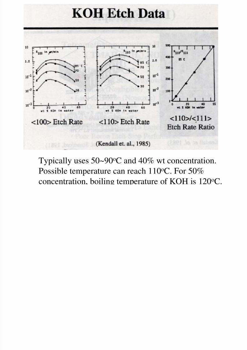
Typically uses 50~90
o
C and 40% wt concentration.Possible temperature can reach 110oC. For 50%
concentration boilin tem erature of KOH is 120oC.

8/8/2019 Silicon 012
http://slidepdf.com/reader/full/silicon-012 39/71

8/8/2019 Silicon 012
http://slidepdf.com/reader/full/silicon-012 40/71

8/8/2019 Silicon 012
http://slidepdf.com/reader/full/silicon-012 41/71

8/8/2019 Silicon 012
http://slidepdf.com/reader/full/silicon-012 42/71

8/8/2019 Silicon 012
http://slidepdf.com/reader/full/silicon-012 43/71

8/8/2019 Silicon 012
http://slidepdf.com/reader/full/silicon-012 44/71

8/8/2019 Silicon 012
http://slidepdf.com/reader/full/silicon-012 45/71

8/8/2019 Silicon 012
http://slidepdf.com/reader/full/silicon-012 46/71

8/8/2019 Silicon 012
http://slidepdf.com/reader/full/silicon-012 47/71

8/8/2019 Silicon 012
http://slidepdf.com/reader/full/silicon-012 48/71

8/8/2019 Silicon 012
http://slidepdf.com/reader/full/silicon-012 49/71

8/8/2019 Silicon 012
http://slidepdf.com/reader/full/silicon-012 50/71

8/8/2019 Silicon 012
http://slidepdf.com/reader/full/silicon-012 51/71

8/8/2019 Silicon 012
http://slidepdf.com/reader/full/silicon-012 52/71

8/8/2019 Silicon 012
http://slidepdf.com/reader/full/silicon-012 53/71

8/8/2019 Silicon 012
http://slidepdf.com/reader/full/silicon-012 54/71
Other Problems• Undercut
• Corner compensation (refers to convex
corner)
• Alignment

8/8/2019 Silicon 012
http://slidepdf.com/reader/full/silicon-012 55/71

8/8/2019 Silicon 012
http://slidepdf.com/reader/full/silicon-012 56/71
Wafer Bonding

8/8/2019 Silicon 012
http://slidepdf.com/reader/full/silicon-012 57/71

8/8/2019 Silicon 012
http://slidepdf.com/reader/full/silicon-012 58/71
Ref: C. Harendt, W. Appel, H. G. Graf, B. Hofflinger and E. Penteker,J of Micromechanics and Microeng. Vol. 1, 1991, pp.145-151.

8/8/2019 Silicon 012
http://slidepdf.com/reader/full/silicon-012 59/71

8/8/2019 Silicon 012
http://slidepdf.com/reader/full/silicon-012 60/71

8/8/2019 Silicon 012
http://slidepdf.com/reader/full/silicon-012 61/71

8/8/2019 Silicon 012
http://slidepdf.com/reader/full/silicon-012 62/71

8/8/2019 Silicon 012
http://slidepdf.com/reader/full/silicon-012 63/71

8/8/2019 Silicon 012
http://slidepdf.com/reader/full/silicon-012 64/71
Ref: A. Hanneborg, M. Nesse and P. Ohlckers, J. Micromech. Microeng., Vol.
1, 1991, pp.139-144.

8/8/2019 Silicon 012
http://slidepdf.com/reader/full/silicon-012 65/71

8/8/2019 Silicon 012
http://slidepdf.com/reader/full/silicon-012 66/71

8/8/2019 Silicon 012
http://slidepdf.com/reader/full/silicon-012 67/71

8/8/2019 Silicon 012
http://slidepdf.com/reader/full/silicon-012 68/71

8/8/2019 Silicon 012
http://slidepdf.com/reader/full/silicon-012 69/71

8/8/2019 Silicon 012
http://slidepdf.com/reader/full/silicon-012 70/71

8/8/2019 Silicon 012
http://slidepdf.com/reader/full/silicon-012 71/71