Signal conditioning for pyroelectric passive infrared (PIR) sensors
18
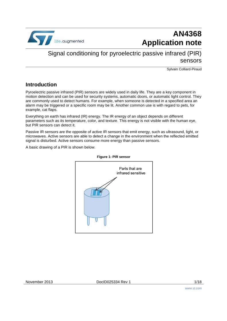
November 2013 DocID025334 Rev 1 1/18 www.st.com AN4368 Application note Signal conditioning for pyroelectric passive infrared (PIR) sensors Sylvain Colliard-Piraud Introduction Pyroelectric passive infrared (PIR) sensors are widely used in daily life. They are a key component in motion detection and can be used for security systems, automatic doors, or automatic light control. They are commonly used to detect humans. For example, when someone is detected in a specified area an alarm may be triggered or a specific room may be lit. Another common use is with regard to pets, for example, cat flaps. Everything on earth has infrared (IR) energy. The IR energy of an object depends on different parameters such as its temperature, color, and texture. This energy is not visible with the human eye, but PIR sensors can detect it. Passive IR sensors are the opposite of active IR sensors that emit energy, such as ultrasound, light, or microwaves. Active sensors are able to detect a change in the environment when the reflected emitted signal is disturbed. Active sensors consume more energy than passive sensors. A basic drawing of a PIR is shown below. Figure 1: PIR sensor
Transcript of Signal conditioning for pyroelectric passive infrared (PIR) sensors
November 2013 DocID025334 Rev 1 1/18
www.st.com
AN4368 Application note
Signal conditioning for pyroelectric passive infrared (PIR) sensors
Sylvain Colliard-Piraud
Introduction
Pyroelectric passive infrared (PIR) sensors are widely used in daily life. They are a key component in motion detection and can be used for security systems, automatic doors, or automatic light control. They are commonly used to detect humans. For example, when someone is detected in a specified area an alarm may be triggered or a specific room may be lit. Another common use is with regard to pets, for example, cat flaps.
Everything on earth has infrared (IR) energy. The IR energy of an object depends on different parameters such as its temperature, color, and texture. This energy is not visible with the human eye, but PIR sensors can detect it.
Passive IR sensors are the opposite of active IR sensors that emit energy, such as ultrasound, light, or microwaves. Active sensors are able to detect a change in the environment when the reflected emitted signal is disturbed. Active sensors consume more energy than passive sensors.
A basic drawing of a PIR is shown below.
Figure 1: PIR sensor
Contents AN4368
2/18 DocID025334 Rev 1
Contents
1 How does the PIR sensor work ...................................................... 3
2 The sensor signal ............................................................................ 4
3 Three-stage architecture for detecting motion.............................. 5
3.1 Stage 1 .............................................................................................. 5
3.2 Stage 2 .............................................................................................. 6
3.3 Stage 3 .............................................................................................. 7
3.4 The best op-amp for each architectural stage ................................... 8
4 Consumption ................................................................................... 9
5 Power-up ........................................................................................ 10
6 Conditioning the signal ................................................................. 11
7 Conclusion ..................................................................................... 15
8 Appendix A .................................................................................... 16
9 Revision history ............................................................................ 17
AN4368 How does the PIR sensor work
DocID025334 Rev 1 3/18
1 How does the PIR sensor work
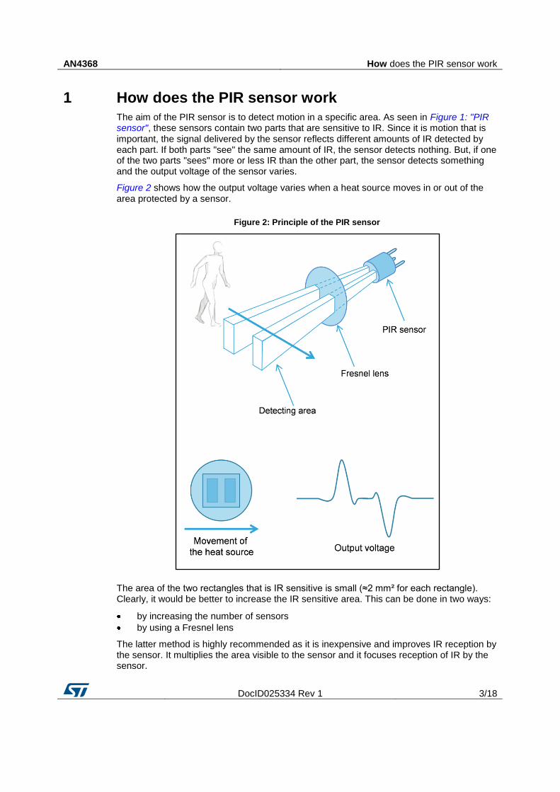
The aim of the PIR sensor is to detect motion in a specific area. As seen in Figure 1: "PIR sensor", these sensors contain two parts that are sensitive to IR. Since it is motion that is important, the signal delivered by the sensor reflects different amounts of IR detected by each part. If both parts "see" the same amount of IR, the sensor detects nothing. But, if one of the two parts "sees" more or less IR than the other part, the sensor detects something and the output voltage of the sensor varies.
Figure 2 shows how the output voltage varies when a heat source moves in or out of the area protected by a sensor.
Figure 2: Principle of the PIR sensor
The area of the two rectangles that is IR sensitive is small (≈2 mm² for each rectangle). Clearly, it would be better to increase the IR sensitive area. This can be done in two ways:
by increasing the number of sensors
by using a Fresnel lens
The latter method is highly recommended as it is inexpensive and improves IR reception by the sensor. It multiplies the area visible to the sensor and it focuses reception of IR by the sensor.
The sensor signal AN4368
4/18 DocID025334 Rev 1
2 The sensor signal
When a body, with a temperature different to ambient, moves into the detection field of a PIR sensor, the sensor provides a small AC signal. This signal is in the range of 1 mVpp. This small voltage is around a DC signal that may significantly vary from one sensor to another. For this reason, it is mandatory to cancel the DC part of the signal and to amplify the AC part. As the signal is disturbed by the environment, a noise filter is useful.
STMicroelectronics’ operational amplifiers (op-amps) can perform all these functions.
The sensor used in this application note is the IRA-E700ST0 from muRata.
AN4368 Three-stage architecture for detecting motion
DocID025334 Rev 1 5/18
3 Three-stage architecture for detecting motion
To detect motion, a three-stage architecture based on op-amps is used to condition the signal of a PIR sensor. This architecture is explained below.
3.1 Stage 1
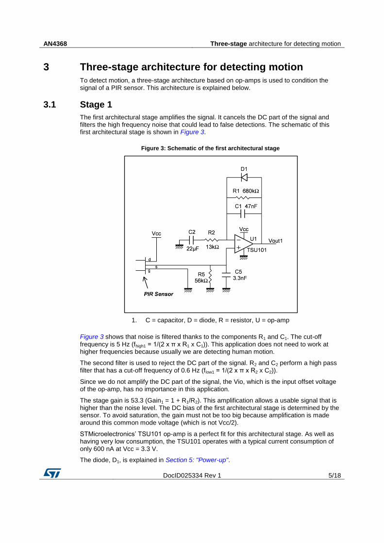
The first architectural stage amplifies the signal. It cancels the DC part of the signal and filters the high frequency noise that could lead to false detections. The schematic of this first architectural stage is shown in Figure 3.
Figure 3: Schematic of the first architectural stage
1. C = capacitor, D = diode, R = resistor, U = op-amp
Figure 3 shows that noise is filtered thanks to the components R1 and C1. The cut-off frequency is 5 Hz (fhigh1 = 1/(2 x π x R1 x C1)). This application does not need to work at higher frequencies because usually we are detecting human motion.
The second filter is used to reject the DC part of the signal. R2 and C2 perform a high pass filter that has a cut-off frequency of 0.6 Hz (flow1 = 1/(2 x π x R2 x C2)).
Since we do not amplify the DC part of the signal, the Vio, which is the input offset voltage of the op-amp, has no importance in this application.
The stage gain is 53.3 (Gain1 = 1 + R1/R2). This amplification allows a usable signal that is higher than the noise level. The DC bias of the first architectural stage is determined by the sensor. To avoid saturation, the gain must not be too big because amplification is made around this common mode voltage (which is not Vcc/2).
STMicroelectronics’ TSU101 op-amp is a perfect fit for this architectural stage. As well as having very low consumption, the TSU101 operates with a typical current consumption of only 600 nA at Vcc = 3.3 V.
The diode, D1, is explained in Section 5: "Power-up".
Three-stage architecture for detecting motion AN4368
6/18 DocID025334 Rev 1
3.2 Stage 2
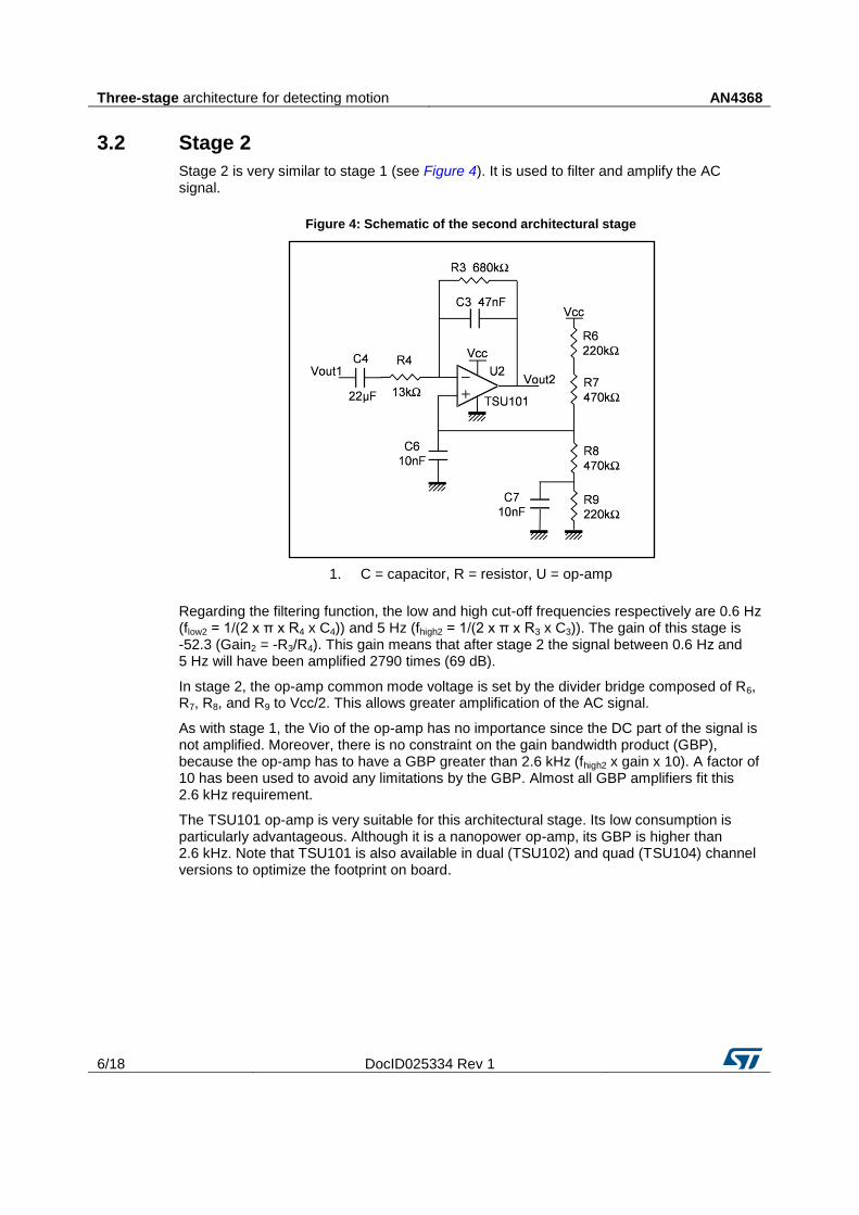
Stage 2 is very similar to stage 1 (see Figure 4). It is used to filter and amplify the AC signal.
Figure 4: Schematic of the second architectural stage
1. C = capacitor, R = resistor, U = op-amp
Regarding the filtering function, the low and high cut-off frequencies respectively are 0.6 Hz (flow2 = 1/(2 x π x R4 x C4)) and 5 Hz (fhigh2 = 1/(2 x π x R3 x C3)). The gain of this stage is -52.3 (Gain2 = -R3/R4). This gain means that after stage 2 the signal between 0.6 Hz and 5 Hz will have been amplified 2790 times (69 dB).
In stage 2, the op-amp common mode voltage is set by the divider bridge composed of R6, R7, R8, and R9 to Vcc/2. This allows greater amplification of the AC signal.
As with stage 1, the Vio of the op-amp has no importance since the DC part of the signal is not amplified. Moreover, there is no constraint on the gain bandwidth product (GBP), because the op-amp has to have a GBP greater than 2.6 kHz (fhigh2 x gain x 10). A factor of 10 has been used to avoid any limitations by the GBP. Almost all GBP amplifiers fit this 2.6 kHz requirement.
The TSU101 op-amp is very suitable for this architectural stage. Its low consumption is particularly advantageous. Although it is a nanopower op-amp, its GBP is higher than 2.6 kHz. Note that TSU101 is also available in dual (TSU102) and quad (TSU104) channel versions to optimize the footprint on board.
AN4368 Three-stage architecture for detecting motion
DocID025334 Rev 1 7/18
3.3 Stage 3
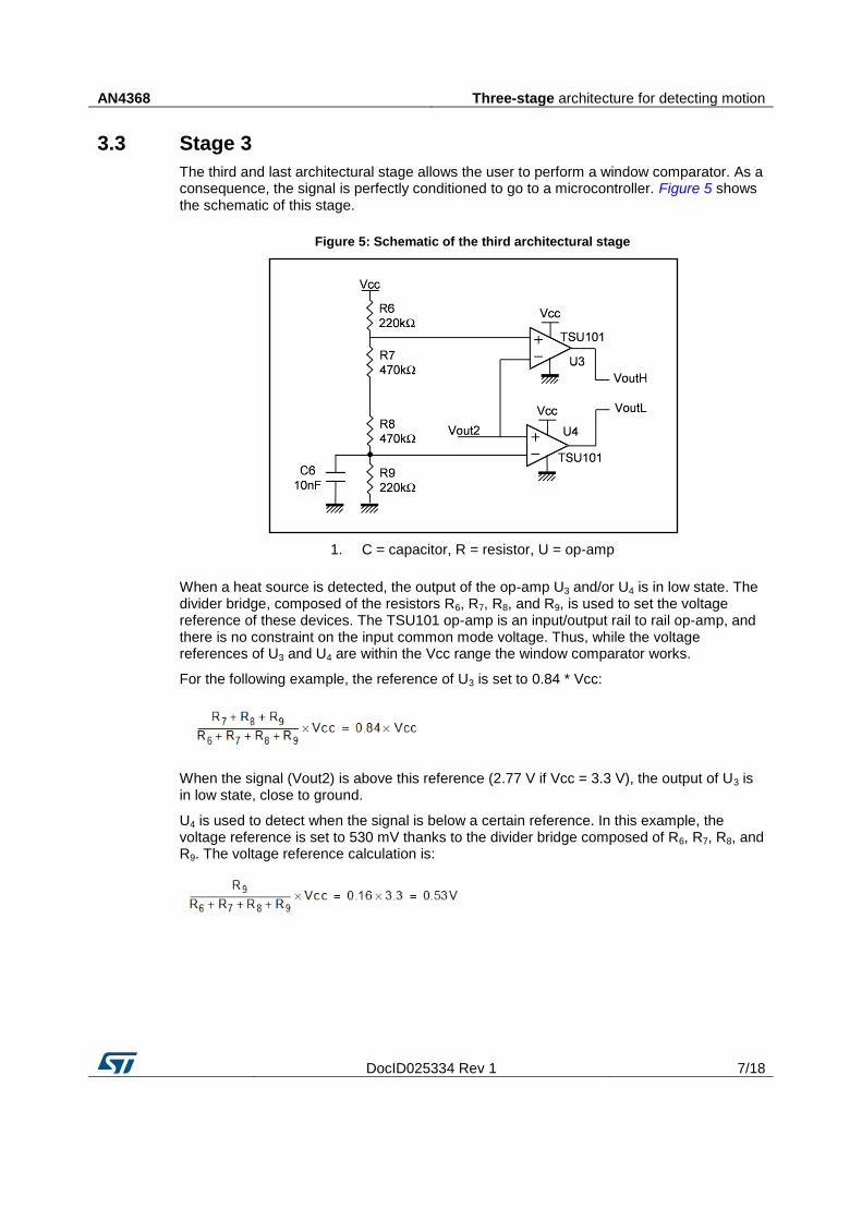
The third and last architectural stage allows the user to perform a window comparator. As a consequence, the signal is perfectly conditioned to go to a microcontroller. Figure 5 shows the schematic of this stage.
Figure 5: Schematic of the third architectural stage
1. C = capacitor, R = resistor, U = op-amp
When a heat source is detected, the output of the op-amp U3 and/or U4 is in low state. The divider bridge, composed of the resistors R6, R7, R8, and R9, is used to set the voltage reference of these devices. The TSU101 op-amp is an input/output rail to rail op-amp, and there is no constraint on the input common mode voltage. Thus, while the voltage references of U3 and U4 are within the Vcc range the window comparator works.
For the following example, the reference of U3 is set to 0.84 * Vcc:
When the signal (Vout2) is above this reference (2.77 V if Vcc = 3.3 V), the output of U3 is in low state, close to ground.
U4 is used to detect when the signal is below a certain reference. In this example, the voltage reference is set to 530 mV thanks to the divider bridge composed of R6, R7, R8, and R9. The voltage reference calculation is:
Three-stage architecture for detecting motion AN4368
8/18 DocID025334 Rev 1
Thus, when the signal (Vout2) is lower than 0.53 V, the output voltage of U4 is in low state (see Table 1). If only one digital output is required, the user may use a NAND gate connected to the outputs of U3 and U4.
Table 1: NAND truth table
Vout2 Output U3 Output U4 Output NAND gate
Vout2 < 0.16 * Vcc High Low High
0.16 * Vcc < Vout2 < 0.84 * Vcc High High Low
Vout2 > 0.84 * Vcc Low High High
3.4 The best op-amp for each architectural stage
The schematics show that a quad op-amp is a good choice for the current application: one op-amp for stage 1, a second op-amp for stage 2 and two additional op-amps for stage 3. In this respect, the TSU104 is ideal as only one active component is needed for signal conditioning. The one drawback of the TSU104 is that it uses two op-amps for a comparator function but, this is not an issue at such low speeds.
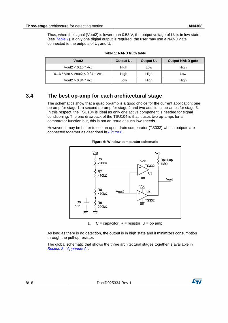
However, it may be better to use an open drain comparator (TS332) whose outputs are connected together as described in Figure 6.
Figure 6: Window comparator schematic
1. C = capacitor, R = resistor, U = op amp
As long as there is no detection, the output is in high state and it minimizes consumption through the pull-up resistor.
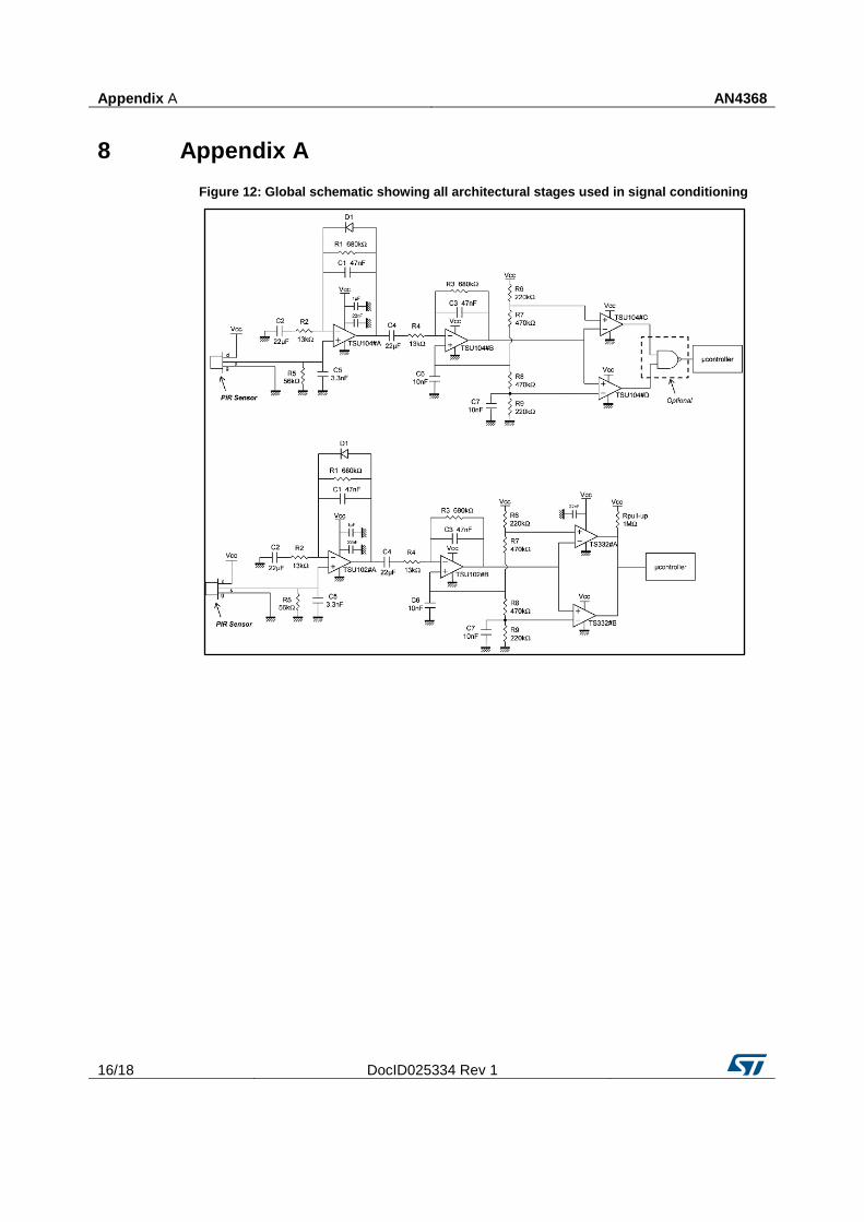
The global schematic that shows the three architectural stages together is available in Section 8: "Appendix A".

AN4368 Consumption
DocID025334 Rev 1 9/18
4 Consumption
Consumption is a key feature for portable applications. The schematics in Section 3: "Three-stage architecture for detecting motion" have been designed to optimize consumption and to be 3.3 V compatible, especially with regard to microcontrollers.
The main consumption is due to the sensor which consumes 19 µA. The rest of the application consumes 4.8 µA as follows:
a TSU104 op-amp consumes 2.4 µA
the divider bridge, composed of R6, R7, R8, and R9, consumes 2.4 µA
The consumption of the divider bridge could be reduced by multiplying the resistor values but at the cost of reliability. When impedances are high, the impact of dust or moisture is higher. These perturbations can create parasitic impedances.
Power-up AN4368
10/18 DocID025334 Rev 1
5 Power-up
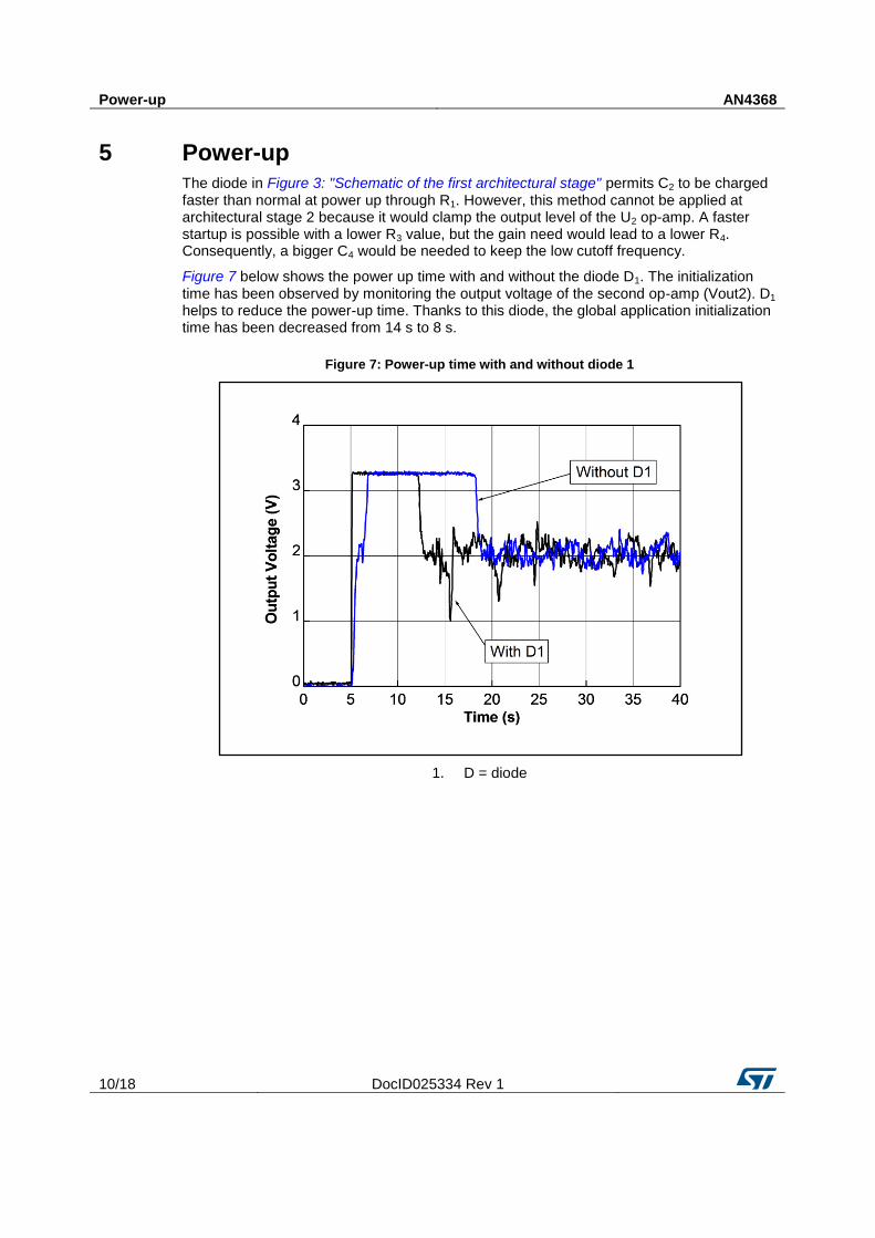
The diode in Figure 3: "Schematic of the first architectural stage" permits C2 to be charged faster than normal at power up through R1. However, this method cannot be applied at architectural stage 2 because it would clamp the output level of the U2 op-amp. A faster startup is possible with a lower R3 value, but the gain need would lead to a lower R4. Consequently, a bigger C4 would be needed to keep the low cutoff frequency.
Figure 7 below shows the power up time with and without the diode D1. The initialization time has been observed by monitoring the output voltage of the second op-amp (Vout2). D1 helps to reduce the power-up time. Thanks to this diode, the global application initialization time has been decreased from 14 s to 8 s.
Figure 7: Power-up time with and without diode 1
1. D = diode
AN4368 Conditioning the signal
DocID025334 Rev 1 11/18
6 Conditioning the signal
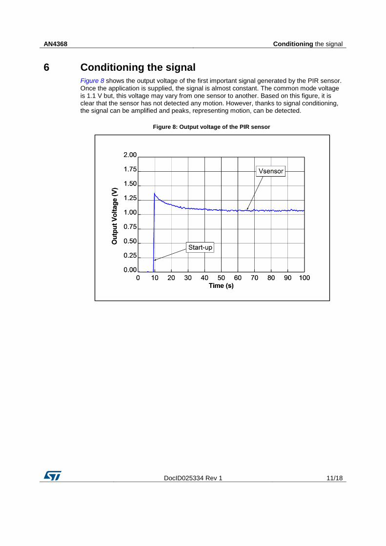
Figure 8 shows the output voltage of the first important signal generated by the PIR sensor. Once the application is supplied, the signal is almost constant. The common mode voltage is 1.1 V but, this voltage may vary from one sensor to another. Based on this figure, it is clear that the sensor has not detected any motion. However, thanks to signal conditioning, the signal can be amplified and peaks, representing motion, can be detected.
Figure 8: Output voltage of the PIR sensor
Conditioning the signal AN4368
12/18 DocID025334 Rev 1
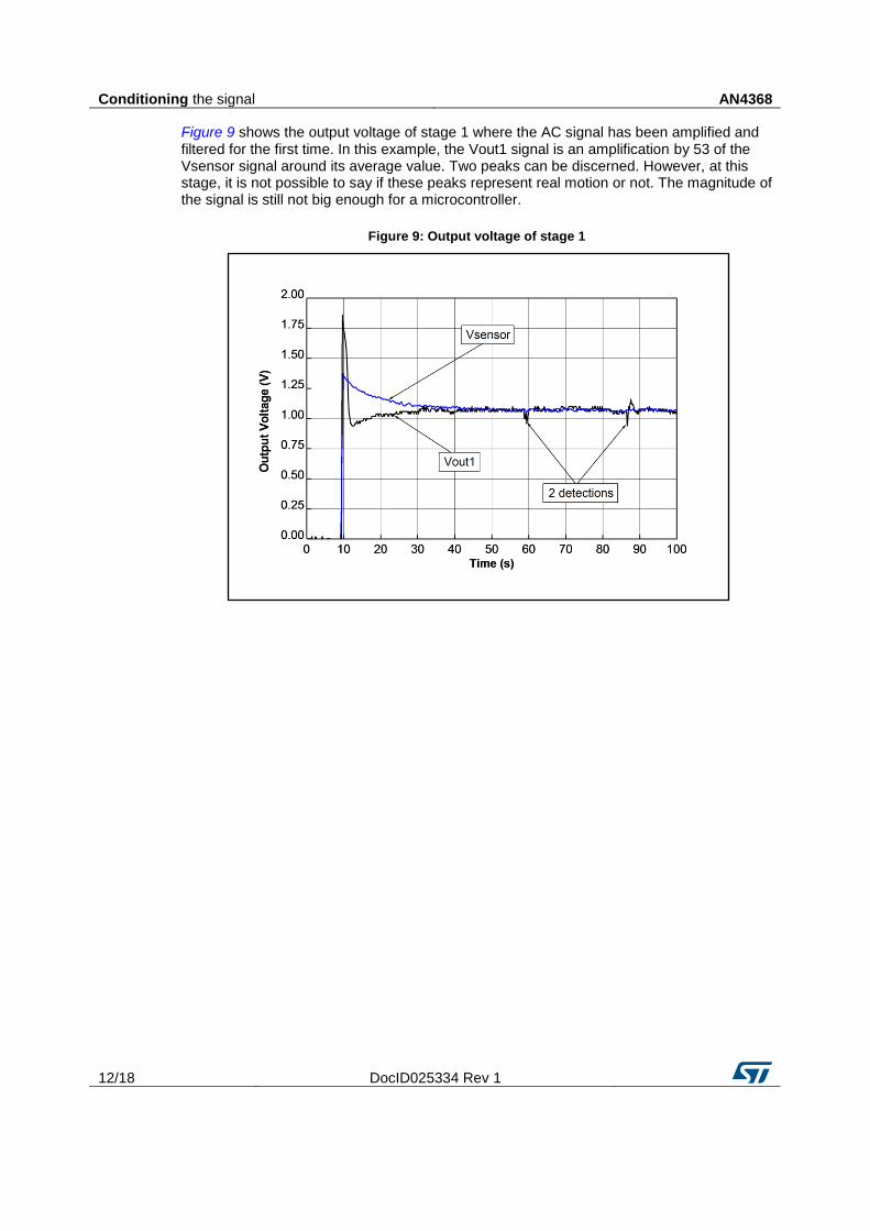
Figure 9 shows the output voltage of stage 1 where the AC signal has been amplified and filtered for the first time. In this example, the Vout1 signal is an amplification by 53 of the Vsensor signal around its average value. Two peaks can be discerned. However, at this stage, it is not possible to say if these peaks represent real motion or not. The magnitude of the signal is still not big enough for a microcontroller.
Figure 9: Output voltage of stage 1
AN4368 Conditioning the signal
DocID025334 Rev 1 13/18
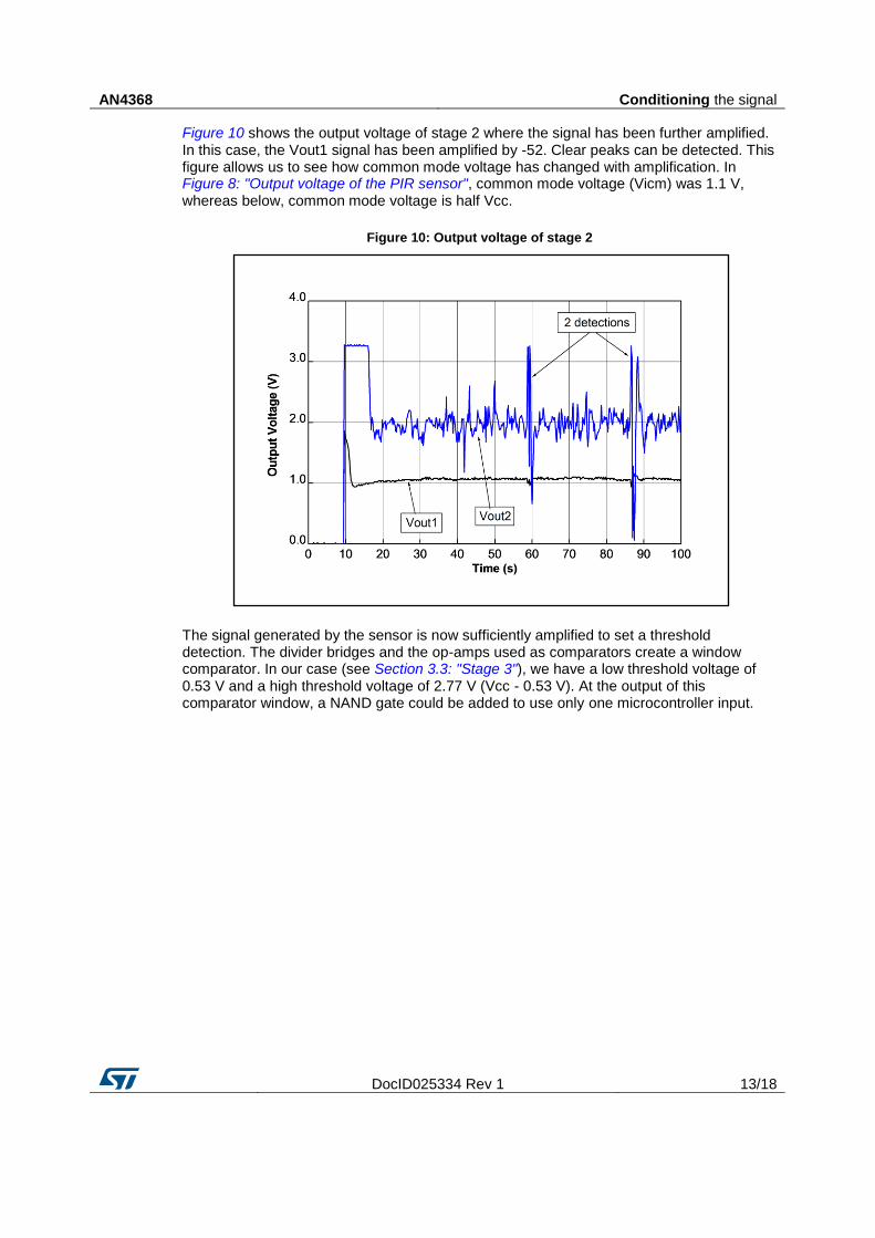
Figure 10 shows the output voltage of stage 2 where the signal has been further amplified. In this case, the Vout1 signal has been amplified by -52. Clear peaks can be detected. This figure allows us to see how common mode voltage has changed with amplification. In Figure 8: "Output voltage of the PIR sensor", common mode voltage (Vicm) was 1.1 V, whereas below, common mode voltage is half Vcc.
Figure 10: Output voltage of stage 2
The signal generated by the sensor is now sufficiently amplified to set a threshold detection. The divider bridges and the op-amps used as comparators create a window comparator. In our case (see Section 3.3: "Stage 3"), we have a low threshold voltage of 0.53 V and a high threshold voltage of 2.77 V (Vcc - 0.53 V). At the output of this comparator window, a NAND gate could be added to use only one microcontroller input.
Conditioning the signal AN4368
14/18 DocID025334 Rev 1
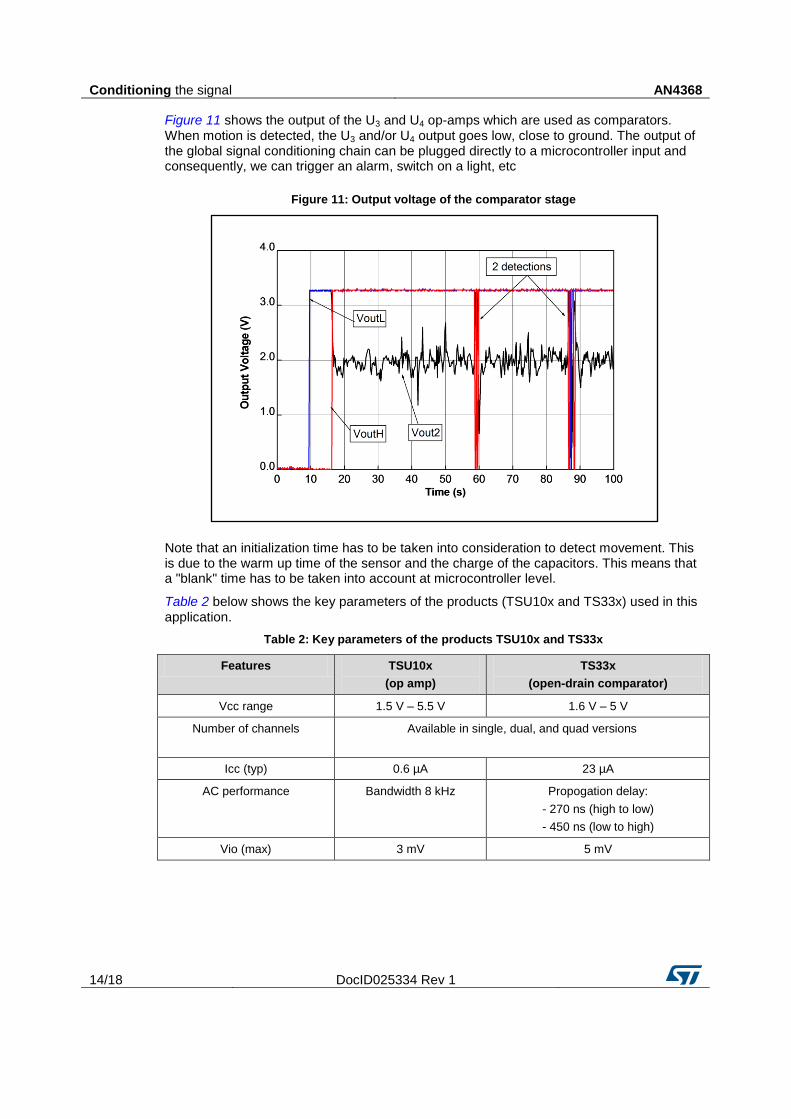
Figure 11 shows the output of the U3 and U4 op-amps which are used as comparators. When motion is detected, the U3 and/or U4 output goes low, close to ground. The output of the global signal conditioning chain can be plugged directly to a microcontroller input and consequently, we can trigger an alarm, switch on a light, etc
Figure 11: Output voltage of the comparator stage
Note that an initialization time has to be taken into consideration to detect movement. This is due to the warm up time of the sensor and the charge of the capacitors. This means that a "blank" time has to be taken into account at microcontroller level.
Table 2 below shows the key parameters of the products (TSU10x and TS33x) used in this application.
Table 2: Key parameters of the products TSU10x and TS33x
Features TSU10x
(op amp)
TS33x
(open-drain comparator)
Vcc range 1.5 V – 5.5 V 1.6 V – 5 V
Number of channels Available in single, dual, and quad versions
Icc (typ) 0.6 µA 23 µA
AC performance Bandwidth 8 kHz Propogation delay:
- 270 ns (high to low)
- 450 ns (low to high)
Vio (max) 3 mV 5 mV

AN4368 Conclusion
DocID025334 Rev 1 15/18
7 Conclusion
PIR sensors are widely used and require op-amps to amplify and filter the signal they generate which is noisy and small in amplitude. Op-amps or comparators can be used to compare the amplified signal with threshold voltages before it goes into the I/O of a microcontroller (i.e. there is no need for an analog-to-digital converter).
With the TSU104 (quad op-amp) or TSU102 (dual op-amp) and TS332 (dual comparator), an application can be designed which is compliant with a 3.3 V microcontroller. The whole analog chain consumes only 24 µA with a micropower TSU104.
STMicroelectronics provides nanopower op-amps and comparators for portable applications. STMicroelectronics can also provide op-amps and comparators with a bigger bandwidth, a higher output current, a wider Vcc range, or even op-amps that are automotive grade compliant. The wide STMicroelectronics portfolio meets all needs.
Appendix A AN4368
16/18 DocID025334 Rev 1
8 Appendix A
Figure 12: Global schematic showing all architectural stages used in signal conditioning

AN4368 Revision history
DocID025334 Rev 1 17/18
9 Revision history
Table 3: Document revision history
Date Revision Changes
25-Nov-2013 1 Initial release
AN4368
18/18 DocID025334 Rev 1
Please Read Carefully
Information in this document is provided solely in connection with ST products. STMicroelectronics NV and its subsidiaries ("ST") reserve the right to make changes, corrections, modifications or improvements, to this document, and the products and services described herein at any time, without notice.
All ST products are sold pursuant to ST’s terms and conditions of sale.
Purchasers are solely responsible for the choice, selection and use of the ST products and services described herein, and ST assumes no liability whatsoever relating to the choice, selection or use of the ST products and services described herein.
No license, express or implied, by estoppel or otherwise, to any intellectual property rights is granted under this document. If any part of this document refers to any third party products or services it shall not be deemed a license grant by ST for the use of such third party products or services, or any intellectual property contained therein or considered as a warranty covering the use in any manner whatsoever of such third party products or services or any intellectual property contained therein.
UNLESS OTHERWISE SET FORTH IN ST’S TERMS AND CONDITIONS OF SALE ST DISCLAIMS ANY EXPRESS OR IMPLIED WARRANTY WITH RESPECT TO THE USE AND/OR SALE OF ST PRODUCTS INCLUDING WITHOUT LIMITATION IMPLIED WARRANTIES OF MERCHANTABILITY, FITNESS FOR A PARTICULAR PURPOSE (AND THEIR EQUIVALENTS UNDER THE LAWS OF ANY JURISDICTION), OR INFRINGEMENT OF ANY PATENT, COPYRIGHT OR OTHER INTELLECTUAL PROPERTY RIGHT.
ST PRODUCTS ARE NOT DESIGNED OR AUTHORIZED FOR USE IN: (A) SAFETY CRITICAL APPLICATIONS SUCH AS LIFE SUPPORTING, ACTIVE IMPLANTED DEVICES OR SYSTEMS WITH PRODUCT FUNCTIONAL SAFETY REQUIREMENTS; (B) AERONAUTIC APPLICATIONS; (C) AUTOMOTIVE APPLICATIONS OR ENVIRONMENTS, AND/OR (D) AEROSPACE APPLICATIONS OR ENVIRONMENTS. WHERE ST PRODUCTS ARE NOT DESIGNED FOR SUCH USE, THE PURCHASER SHALL USE PRODUCTS AT PURCHASER’S SOLE RISK, EVEN IF ST HAS BEEN INFORMED IN WRITING OF SUCH USAGE, UNLESS A PRODUCT IS EXPRESSLY DESIGNATED BY ST AS BEING INTENDED FOR "AUTOMOTIVE, AUTOMOTIVE SAFETY OR MEDICAL" INDUSTRY DOMAINS ACCORDING TO ST PRODUCT DESIGN SPECIFICATIONS. PRODUCTS FORMALLY ESCC, QML OR JAN QUALIFIED ARE DEEMED SUITABLE FOR USE IN AEROSPACE BY THE CORRESPONDING GOVERNMENTAL AGENCY.
Resale of ST products with provisions different from the statements and/or technical features set forth in this document shall immediately void any warranty granted by ST for the ST product or service described herein and shall not create or extend in any manner whatsoever, any liability of ST.
ST and the ST logo are trademarks or registered trademarks of ST in various countries.
Information in this document supersedes and replaces all information previously supplied.
The ST logo is a registered trademark of STMicroelectronics. All other names are the property of their respective owners.
© 2013 STMicroelectronics - All rights reserved
STMicroelectronics group of companies
Australia - Belgium - Brazil - Canada - China - Czech Republic - Finland - France - Germany - Hong Kong - India - Israel - Italy - Japan - Malaysia - Malta - Morocco - Philippines - Singapore - Spain - Sweden - Switzerland - United Kingdom - United
States of America
www.st.com