SiGe Semiconductor Devices for Cryogenic Power Electronics
31
SiGe Semiconductor Devices for Cryogenic Power Electronics Electrochemical Society Seventh International Symposium on Low Temperature Electronics 14 October 2003, Orlando, Florida
-
Upload
darius-pope -
Category
Documents
-
view
72 -
download
0
description
Electrochemical Society Seventh International Symposium on Low Temperature Electronics. SiGe Semiconductor Devices for Cryogenic Power Electronics. 14 October 2003, Orlando, Florida. R. R. Ward, W. J. Dawson, L. Zhu, R. K. Kirschman GPD Optoelectronics Corp., Salem, New Hampshire - PowerPoint PPT Presentation
Transcript of SiGe Semiconductor Devices for Cryogenic Power Electronics
SiGe Semiconductor Devices
for
Cryogenic Power Electronics
Electrochemical Society
Seventh International Symposium on Low Temperature Electronics
14 October 2003, Orlando, Florida
2
R. R. Ward, W. J. Dawson, L. Zhu, R. K. Kirschman
GPD Optoelectronics Corp., Salem, New Hampshire
O. Mueller
LTE–Low Temperature Electronics, Ballston Lake, New York
R. L. Patterson, J. E. Dickman
NASA Glenn Research Center, Cleveland, Ohio
A. Hammoud
QSS Group Inc., Cleveland, Ohio
Supported by NASA Glenn Research Center and ONR/DARPA

Why use SiGe?

4
Why SiGe Devices?
• Si-Based Circuits Demonstrated, but only > 77 K
• Standard Si Bipolar Devices Cease Operation < ~100 K
• Applications Require Operation < 77 K, to ~30 – 40 K
• Possible Materials for < 77 K are Ge and SiGe
5
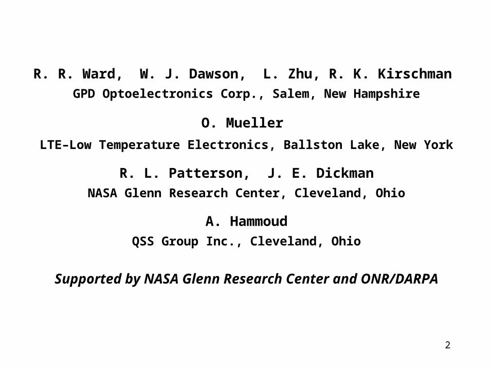
Why SiGe Devices?
• SiGe Devices Can Operate to Lowest Cryogenic
Temperatures (~ 0 K)
• All Device Types – Diodes, Field-Effect Transistors,
Bipolar Transistors
• Highly Compatible with Si Processing
• Can Optimize Devices for Cryogenic Applications
by Selective Use of Ge, Si, SiGe
• SiGe Provides Additional Flexibility through
Band-Gap Engineering (% of Ge)

Development Program
7
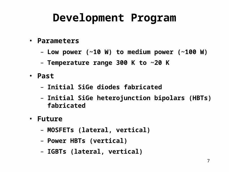
Development Program
• Parameters
– Low power (~10 W) to medium power (~100 W)
– Temperature range 300 K to ~20 K
• Past
– Initial SiGe diodes fabricated
– Initial SiGe heterojunction bipolars (HBTs) fabricated
• Future
– MOSFETs (lateral, vertical)
– Power HBTs (vertical)
– IGBTs (lateral, vertical)
SiGe Cryo Power Diodes
9
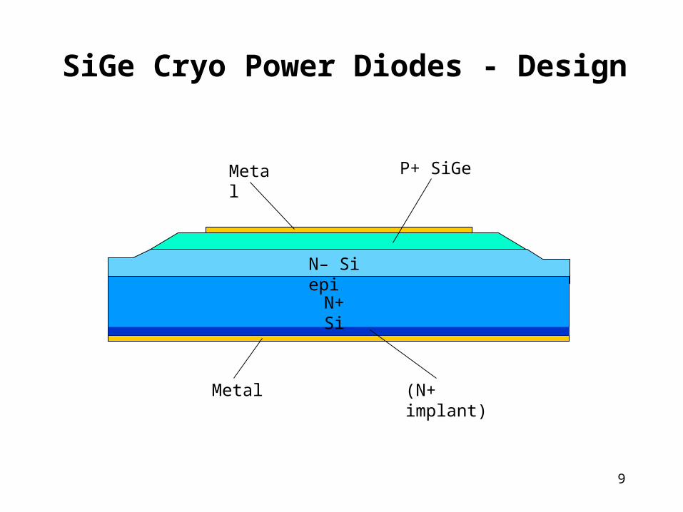
SiGe Cryo Power Diodes - Design
(N+ implant)
P+ SiGe Metal
Metal
N+
N– Si epi
N+ Si
10
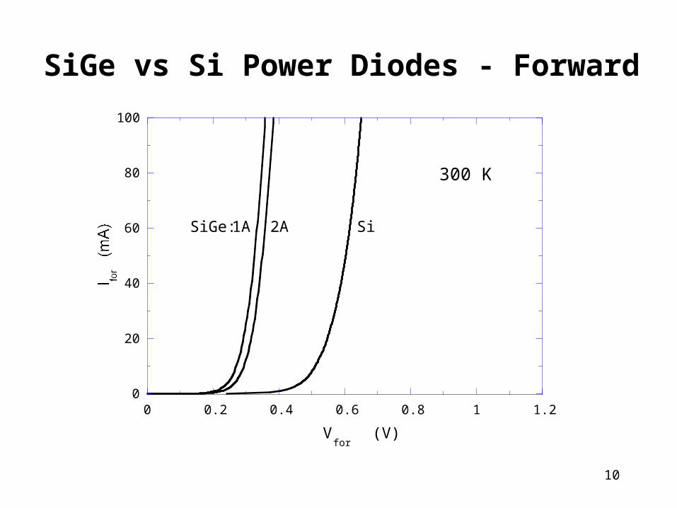
SiGe vs Si Power Diodes - Forward
0
20
40
60
80
100
I (mA)Ifor (mA) RTIf RT (mA)If (mA)
0 0.2 0.4 0.6 0.8 1 1.2
Si
Vfor
(V)
300 K
2ASiGe: 1A
11
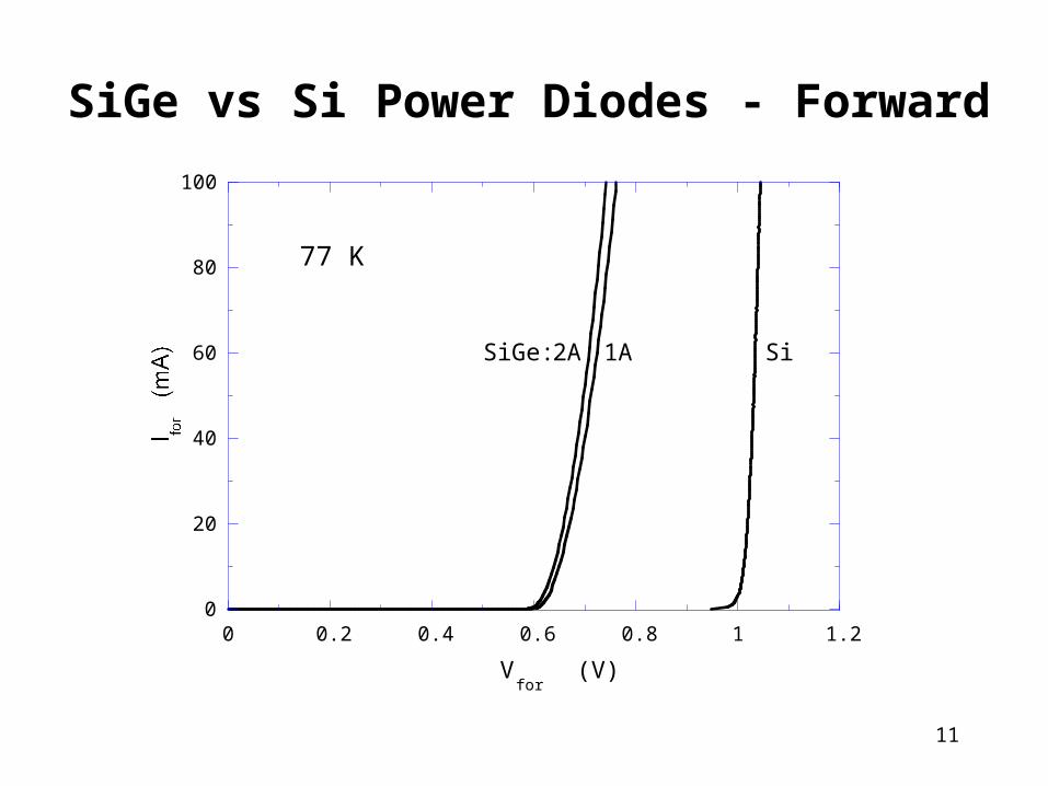
SiGe vs Si Power Diodes - Forward
0
20
40
60
80
100
I (mA)Ifor (mA) LNIf LN (mA)If (mA)
0 0.2 0.4 0.6 0.8 1 1.2
Vfor
(V)
77 K
Si2ASiGe: 1A
12
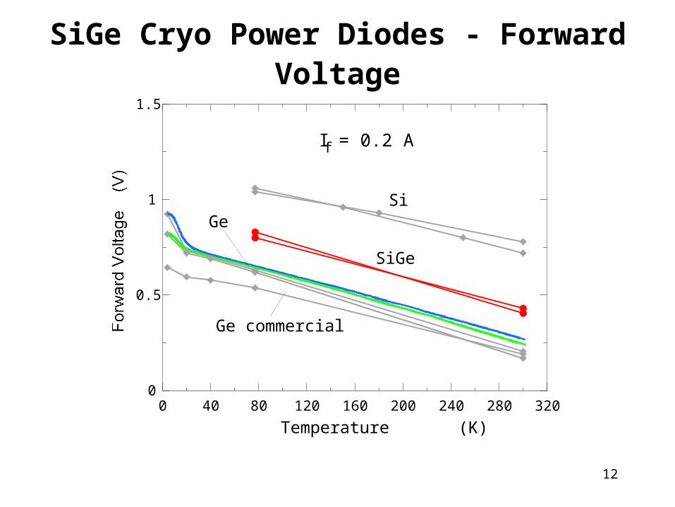
SiGe Cryo Power Diodes - Forward Voltage
0
0.5
1
1.5
0.2 A0.2 A SiVf 0.2 AVf 0.2 A
Vf (0.2 A)Vf (0.2 A)Vf @ 0.2 A (V)
0 40 80 120 160 200 240 280 320
Temperature (K)
Ge commercial
SiGe
If = 0.2 A
SiGe
13
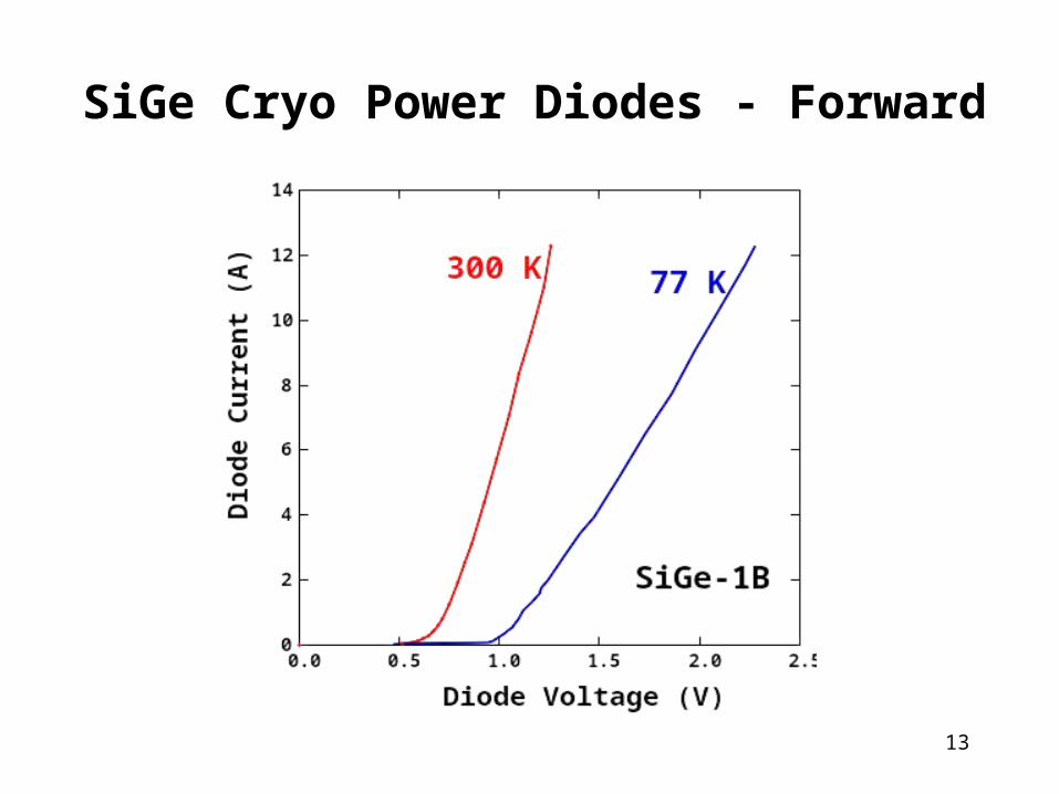
SiGe Cryo Power Diodes - Forward
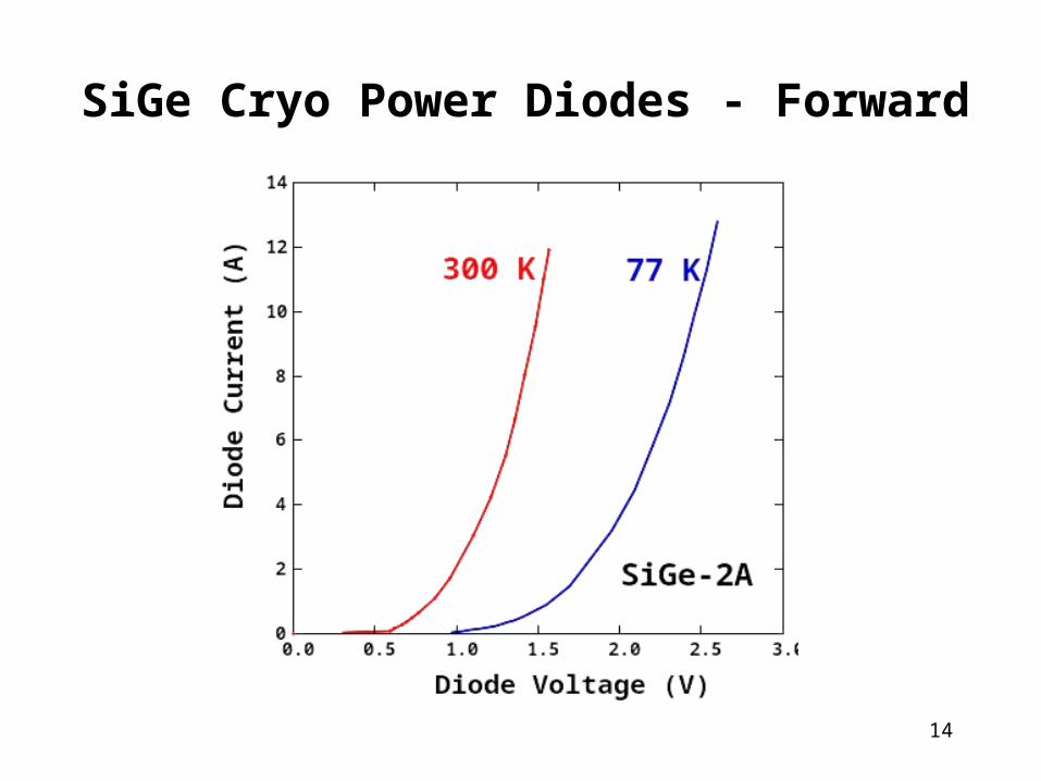
14
SiGe Cryo Power Diodes - Forward
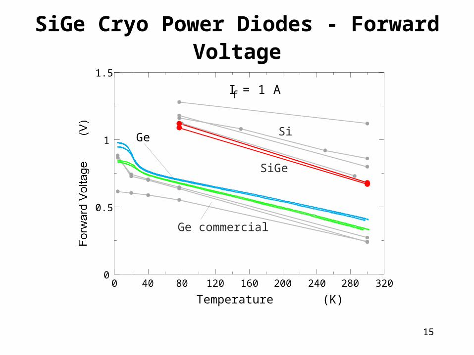
15
0
0.5
1
1.5
1 A lines1 A symbols1 A line Si1 A symbol SiVf 1 A
Vf 1 AVf (1 A)Vf (1 A)Vf @ 1 A (V)
0 40 80 120 160 200 240 280 320
Temperature (K)
Ge commercial
Si
If = 1 A
Ge
SiGe
SiGe Cryo Power Diodes - Forward Voltage
16
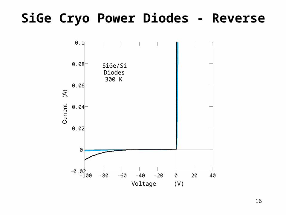
SiGe Cryo Power Diodes - Reverse
-0.02
0
0.02
0.04
0.06
0.08
0.1
-100 -80 -60 -40 -20 0 20 40
Voltage (V)
SiGe/SiDiodes300 K
17
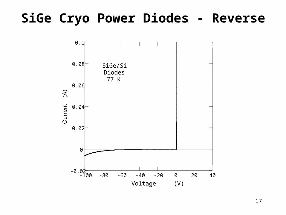
SiGe Cryo Power Diodes - Reverse
-0.02
0
0.02
0.04
0.06
0.08
0.1
-100 -80 -60 -40 -20 0 20 40
Voltage (V)
SiGe/SiDiodes77 K
18
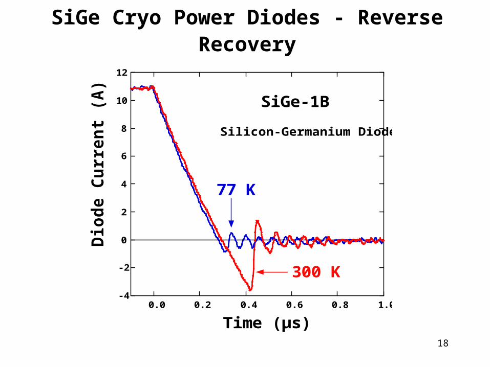
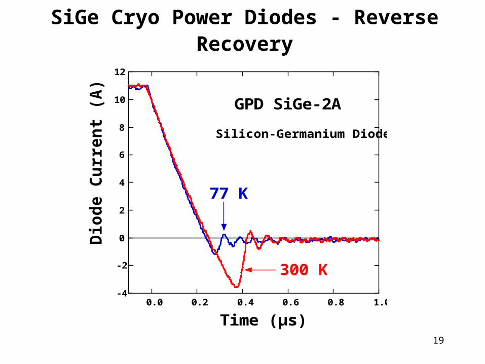
SiGe Cryo Power Diodes - Reverse Recovery
-4
-2
0
2
4
6
8
10
12
0.0 0.2 0.4 0.6 0.8 1.0
Dio
de
Cu
rren
t (A
)
Time (µs)
300 K
77 K
SiGe-1B
Silicon-Germanium Diode
19
SiGe Cryo Power Diodes - Reverse Recovery
-4
-2
0
2
4
6
8
10
12
0.0 0.2 0.4 0.6 0.8 1.0
Dio
de
Cu
rren
t (A
)
Time (µs)
300 K
77 K
GPD SiGe-2A
Silicon-Germanium Diode
20
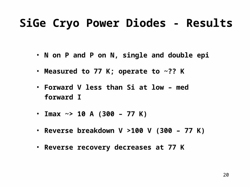
SiGe Cryo Power Diodes - Results
• N on P and P on N, single and double epi
• Measured to 77 K; operate to ~?? K
• Forward V less than Si at low – med forward I
• Imax ~> 10 A (300 – 77 K)
• Reverse breakdown V >100 V (300 – 77 K)
• Reverse recovery decreases at 77 K
SiGe Cryo Heterojunction Bipolar Transistors (HBTs)
22
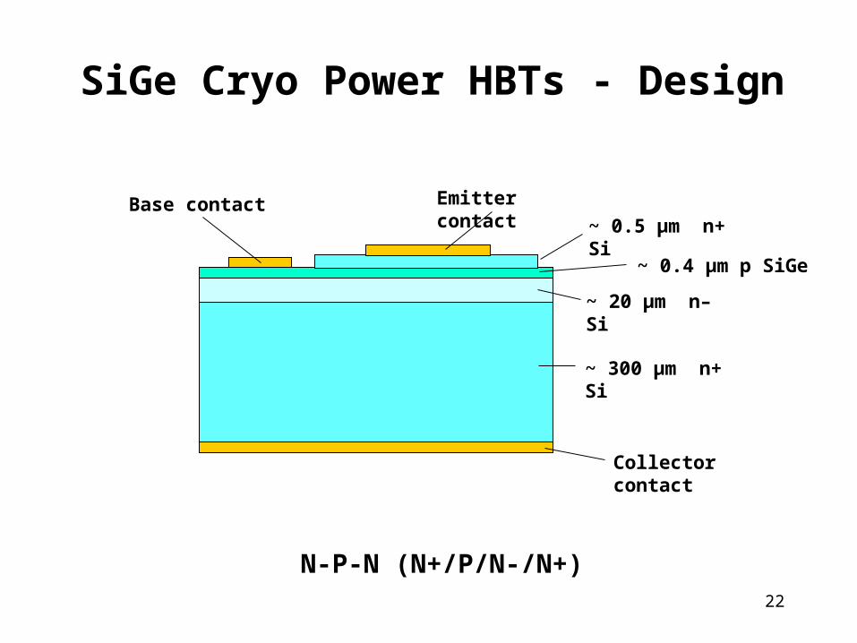
SiGe Cryo Power HBTs - Design
~ 0.5 μm n+ Si
~ 0.4 μm p SiGe
~ 20 μm n– Si
Emitter contact
~ 300 μm n+ Si
Collector contact
Base contact
N-P-N (N+/P/N-/N+)
23
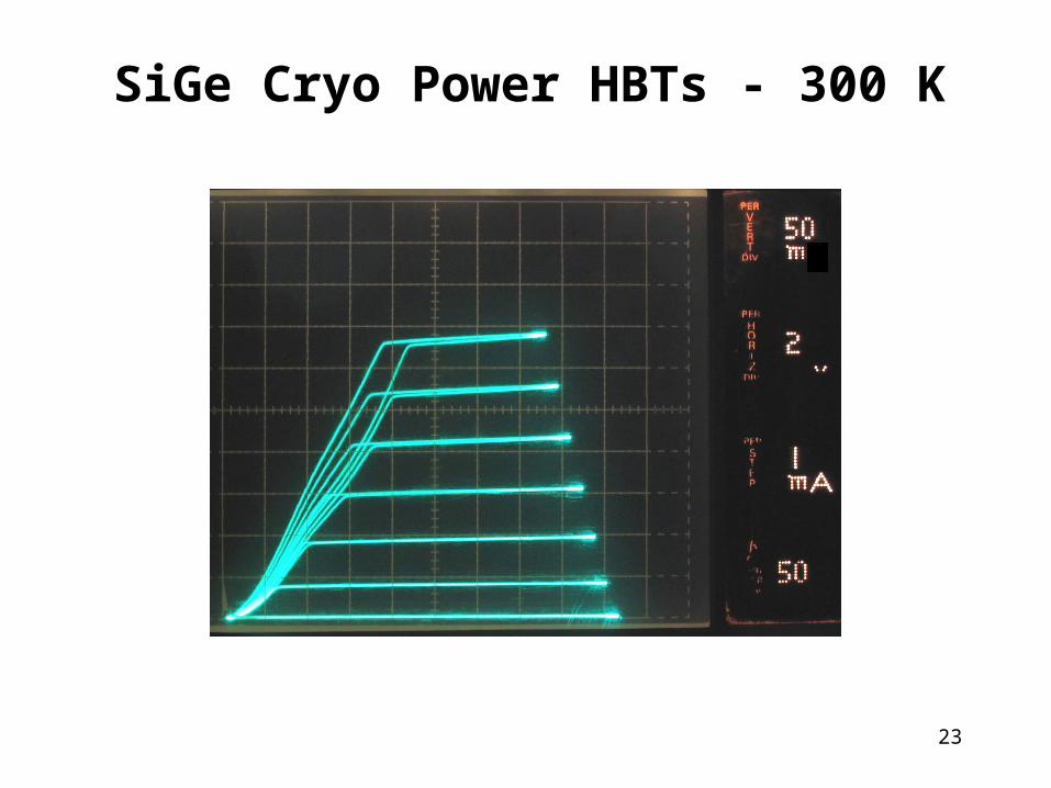
SiGe Cryo Power HBTs - 300 K
24
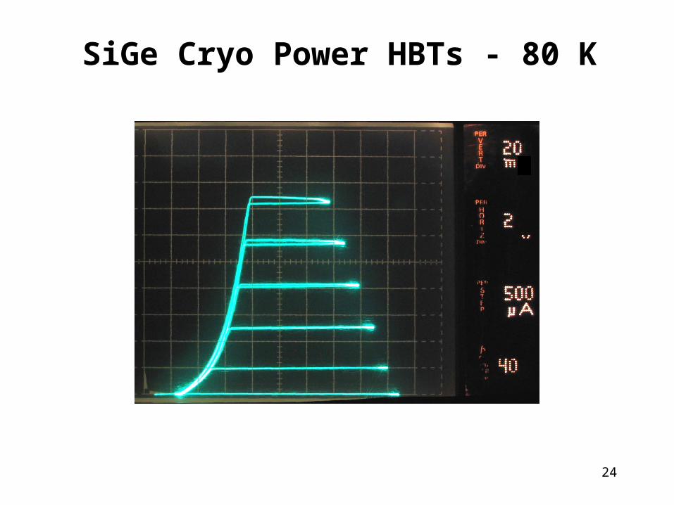
SiGe Cryo Power HBTs - 80 K
25
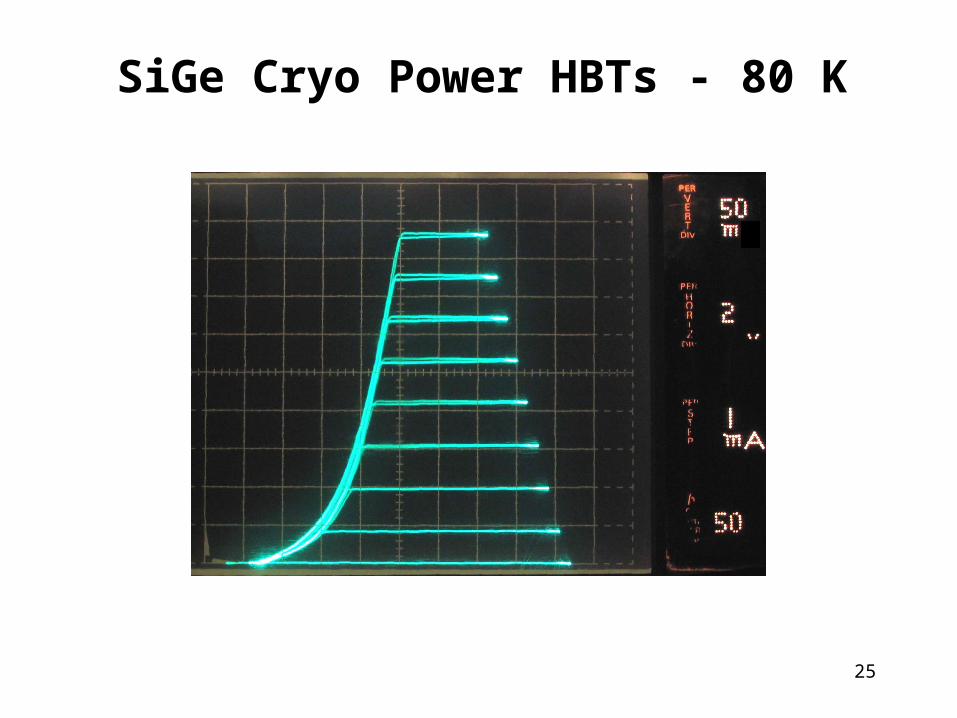
SiGe Cryo Power HBTs - 80 K
26
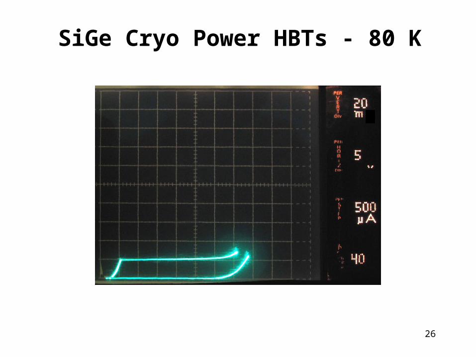
SiGe Cryo Power HBTs - 80 K
27
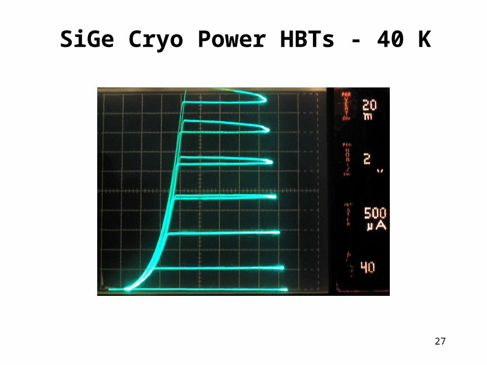
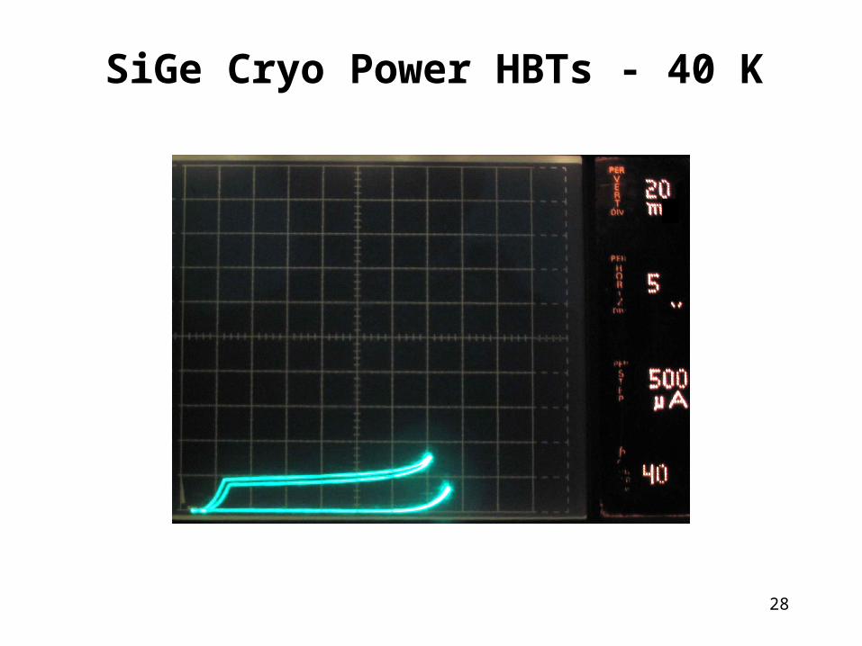
SiGe Cryo Power HBTs - 40 K
28
SiGe Cryo Power HBTs - 40 K
29
SiGe Cryo Power HBTs - Results
• Initial fabrication
• NPN
• Operate down to ~40 K
• Power ~5 W, limited by package
• I max ~> 0.4 A (300 – 40 K)
• V forward breakdown ~>30 V (300 – 40 K)
• Need improved contacts
30
Cryo Power SiGe Devices - Plans
• HBTs
– Improve HBT contacts, extend operation to ~20 K
– Larger area, I max to 10 A (300 – 20 K)
– V forward breakdown >100 V (300 – 20 K)
– High-power cryogenic packaging
• Additional Devices
– MOSFETs
– IGBTs
– Medium power, 300 – 20 K operation
31
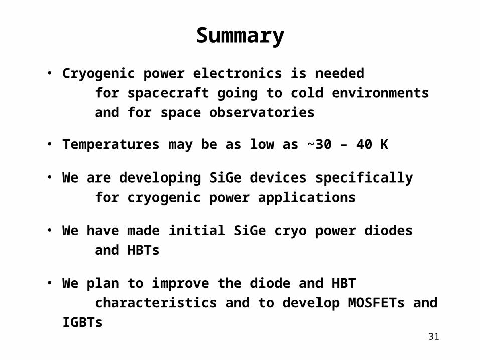
Summary
• Cryogenic power electronics is needed
for spacecraft going to cold environments
and for space observatories
• Temperatures may be as low as ~30 – 40 K
• We are developing SiGe devices specifically
for cryogenic power applications
• We have made initial SiGe cryo power diodes
and HBTs
• We plan to improve the diode and HBT
characteristics and to develop MOSFETs and IGBTs