SIG100 Evaluation Board Manual - Yamar Electronics
10
Preliminary, Data may be changed without notice - Proprietary information of Yamar Electronics Ltd. © 2020-2021 Yamar Electronics Ltd. 1 MD-SIG100 R 0.5 www.yamar.com Tel: +972-3-5445294 Fax: +972-3-5445279 1. Overview The SIG100 evaluation board (EVB) allows easy testing of the SIG100 device in a system. Multiple SIG100 EVBs can communicate over a vehicle's DC powerline using the UART/LIN protocol. Figure 1 presents the EVB. This manual describes how to use and interface with the EVB. The SIG100 data sheet is a reference to this document. Figure 1 - SIG100 EVB 2. SIG100 EVB Description 2.1 Block Diagram Description The EVB contains all the required hardware for device operation such as a line protection network, filter, 16MHz crystal, and a 3.3V switching power supply. The board is a physical layer of the UART/LIN protocol over DC powerlines at data rates of up to 115.2kbit/s. The SIG100 may also be used as a new physical layer to the LIN protocol. The EVB connects directly to a UART/LIN controller (ECU) through its TX and RX pins connected to HDI and HDO pins in the J1 Host connector. The EVB block diagram is depicted in Figure 2. Figure 2 - SIG100 EVB Blocks EVB Manual SIG100 Evaluation Board Manual
Transcript of SIG100 Evaluation Board Manual - Yamar Electronics
Preliminary, Data may be changed without notice - Proprietary information of Yamar Electronics Ltd.
© 2020-2021 Yamar Electronics Ltd. 1 MD-SIG100 R 0.5 www.yamar.com Tel: +972-3-5445294 Fax: +972-3-5445279
1. Overview
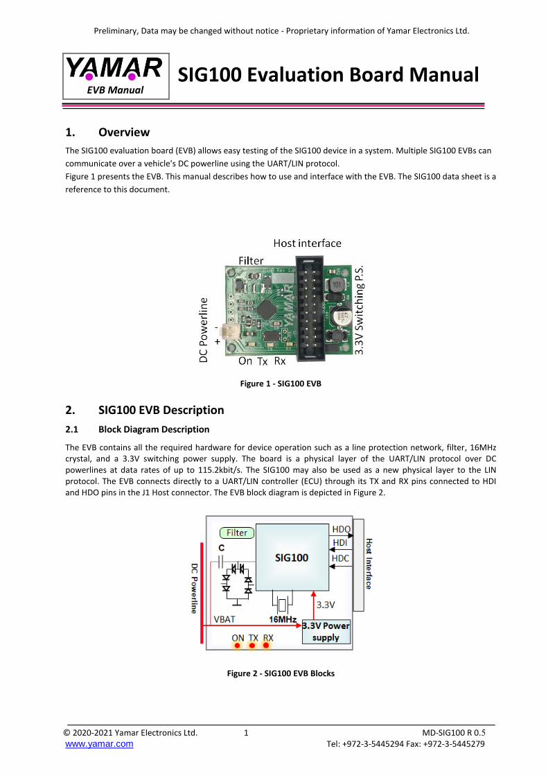
The SIG100 evaluation board (EVB) allows easy testing of the SIG100 device in a system. Multiple SIG100 EVBs can
communicate over a vehicle's DC powerline using the UART/LIN protocol.
Figure 1 presents the EVB. This manual describes how to use and interface with the EVB. The SIG100 data sheet is a
reference to this document.
Figure 1 - SIG100 EVB
2. SIG100 EVB Description
2.1 Block Diagram Description
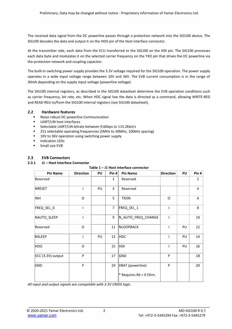
The EVB contains all the required hardware for device operation such as a line protection network, filter, 16MHz crystal, and a 3.3V switching power supply. The board is a physical layer of the UART/LIN protocol over DC powerlines at data rates of up to 115.2kbit/s. The SIG100 may also be used as a new physical layer to the LIN protocol. The EVB connects directly to a UART/LIN controller (ECU) through its TX and RX pins connected to HDI and HDO pins in the J1 Host connector. The EVB block diagram is depicted in Figure 2.
Figure 2 - SIG100 EVB Blocks
EVB Manual SIG100 Evaluation Board Manual
Preliminary, Data may be changed without notice - Proprietary information of Yamar Electronics Ltd.
© 2020-2021 Yamar Electronics Ltd. 2 MD-SIG100 R 0.5 www.yamar.com Tel: +972-3-5445294 Fax: +972-3-5445279
The received data signal from the DC powerline passes through a protection network into the SIG100 device. The
SIG100 decodes the data and output it on the HDO pin of the Host interface connector.
At the transmitter side, each data from the ECU transferred to the SIG100 on the HDI pin. The SIG100 processes
each data byte and modulates it on the selected carrier frequency on the TXO pin that drives the DC powerline via
the protection network and coupling capacitor.
The built-in switching power supply provides the 3.3V voltage required for the SIG100 operation. The power supply
operates in a wide input voltage range between 10V and 36V. The EVB current consumption is in the range of
30mA depending on the supply input voltage (powerline voltage).
The SIG100 internal registers, as described in the SIG100 datasheet determine the EVB operation conditions such
as carrier frequency, bit rate, etc. When HDC signal low the data is directed as a command, allowing WRITE-REG
and READ-REG to/from the SIG100 internal registers (see SIG100 datasheet).
2.2 Hardware features Noise robust DC powerline Communication UART/LIN host interfaces Selectable UART/LIN bitrate between 9.6Kbps to 115.2kbit/s 251 selectable operating frequencies (5MHz to 30MHz, 100kHz spacing) 10V to 36V operation using switching power supply Indication LEDs Small size EVB
2.3 EVB Connectors 2.3.1 J1 – Host Interface Connector
Table 1 – J1 Host interface connector
Pin Name Direction PU Pin # Pin Name Direction PU Pin #
Reserved 1 Reserved 2
NRESET I PU 3 Reserved 4
INH O 5 TXON O 6
FREQ_SEL_0 I 7 FREQ_SEL_1 I 8
NAUTO_SLEEP I 9 N_AUTO_FREQ_CHANGE I 10
Reserved O 11 NLOOPBACK I PU 12
NSLEEP I PU 13 HDC I PU 14
HDO O 15 HDI I PU 16
VCC (3.3V) output P 17 GND P 18
GND P 19 VBAT (powerline)
* Requires R6 = 0 Ohm.
P 20
All input and output signals are compatible with 3.3V CMOS logic.

Preliminary, Data may be changed without notice - Proprietary information of Yamar Electronics Ltd.
© 2020-2021 Yamar Electronics Ltd. 3 MD-SIG100 R 0.5 www.yamar.com Tel: +972-3-5445294 Fax: +972-3-5445279
2.3.2 J2 – DC Power Line and test points
Table 2 J2 – DC Power Line and test points
Name Pin #
TXO test-pin 1
TXON test-pin 2
RXI test-pin 3
3.3V output from the power supply 4
GND 5
VBAT DC powerline input 6
VBAT input connects the EVB to the DC powerline for communication and power supply.
Power supply requirements: 10V to 36V, minimum 150mA.
2.3.3 Display LEDs
TX LED - Indicates transmission.
RX LED - Data output, indicates reception.
ON LED - Indicates 3.3V power on.
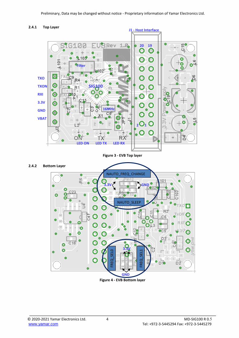
2.4 Mechanical Data The mechanical dimension is depicted in Figure 3.
Preliminary, Data may be changed without notice - Proprietary information of Yamar Electronics Ltd.
© 2020-2021 Yamar Electronics Ltd. 4 MD-SIG100 R 0.5 www.yamar.com Tel: +972-3-5445294 Fax: +972-3-5445279
2.4.1 Top Layer
Figure 3 - EVB Top layer
2.4.2 Bottom Layer
Figure 4 - EVB Bottom layer
TXO
TXON
RXI
3.3V
GND
VBAT
LED ON LED TX LED RX
20 19
2 1
Filter
SIG100
16MHz
J1 - Host Interface
NAUTO_SLEEP
NAUTO_FREQ_CHANGE
GND 3.3V
GND
3.3V
FREQ
_SEL
0
FREQ
_SEL
1

Preliminary, Data may be changed without notice - Proprietary information of Yamar Electronics Ltd.
© 2020-2021 Yamar Electronics Ltd. 5 MD-SIG100 R 0.5 www.yamar.com Tel: +972-3-5445294 Fax: +972-3-5445279
3. EVB Operation
3.1 Configuration
The SIG100 mode of operation and its settings are configured at power-up, reset, and when Host writes into its
internal register (command mode, using the HDC pin). Please refer to the SIG100 datasheet for further
configuration information.
3.2 Interfacing to SIG100 EVB
The SIG100 EVB is designed to interface directly to any UART/LIN controller or through a LIN transceiver.
The Host Interface connector J1 has all the signals required for the EVB proper operation. Three signals are
essential; HDI, HDO, and GND (Data In, Data Out, and Ground). When designing the SIG100 for operation on
setting other than the default (frequency, Sleep, etc.), the HDC pin has to be connected to any output pin of the
UART/LIN controller for setting the SIG100 to the desired operation. Refer to SIG100 datasheet.
When using an external power supply instead/or in parallel to the EVB’s power supply, it is recommended to add
an inductor of at least 22uH in serial to the external power supply to avoid strong attenuation due to the power
supply internal filtering capacitors.
3.3 Interfacing to UART/LIN Controller
The SIG100 interfaces directly to any uC UART/LIN I/O pins (3.3V logic).
The UART/LIN communication protocol uses four pins as described in Table 3.
Table 3 – UART/LIN interface pins
SIG100 Controller Description
HDI TX Data Input from the host controller.
HDC GPO Data/Command select input. When pulled down, the SIG100 enters command mode, enabling access to SIG100 internal registers.
HDO RX Data output to the host controller.
NLOOPBACK GPO Enable loopback of HDI to HDO pin. - When interfacing a UART port, the controller may disable/enable the loopback option. - When interfacing a LIN transceiver, loopback is disabled by keeping the pin floated (internal PU). - When interfacing a LIN controller, tie pin to GND. HDI loops back to HDO.
Figure 5 depicts a typical SIG100 to Controller UART/LIN interface connection.
Figure 5 - Typical SIG100 to UART/LIN Controller interface
Preliminary, Data may be changed without notice - Proprietary information of Yamar Electronics Ltd.
© 2020-2021 Yamar Electronics Ltd. 6 MD-SIG100 R 0.5 www.yamar.com Tel: +972-3-5445294 Fax: +972-3-5445279
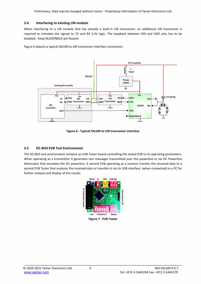
3.4 Interfacing to existing LIN module
When interfacing to a LIN module that has already a built-in LIN transceiver, an additional LIN transceiver is
required to translate the signals to TX and RX 3.3V logic. The loopback between HDI and HDO pins has to be
disabled. Keep NLOOPBACK pin floated.
Figure 6 depicts a typical SIG100 to LIN transceiver interface connection.
Figure 6 - Typical SIG100 to LIN transceiver interface
3.5 DC-BUS EVB Test Environment
The DC-BUS test environment contains an EVB Tester board controlling the tested EVB to its operating parameters.
When operating as a transmitter it generates test messages transmitted over the powerline or via DC Powerline
Attenuator that emulates the DC powerline. A second EVB operating as a receiver transfer the received data to a
second EVB Tester that analyzes the received data or transfers it via its USB interface (when connected) to a PC for
further analysis and display of the results.
Figure 7 - EVB Tester
Preliminary, Data may be changed without notice - Proprietary information of Yamar Electronics Ltd.
© 2020-2021 Yamar Electronics Ltd. 7 MD-SIG100 R 0.5 www.yamar.com Tel: +972-3-5445294 Fax: +972-3-5445279
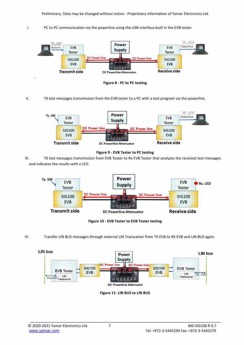
I. PC to PC communication via the powerline using the USB interface built in the EVB tester
.
Figure 8 - PC to PC testing
II. TX test messages transmission from the EVB tester to a PC with a test program via the powerline.
Figure 9 - EVB Tester to PC testing
III. TX test messages transmission from EVB Tester to Rx EVB Tester that analyzes the received test messages
and indicates the results with a LED.
Figure 10 - EVB Tester to EVB Tester testing
IV. Transfer LIN BUS messages through external LIN Transceiver from TX EVB to RX EVB and LIN BUS again.
Figure 11- LIN BUS to LIN BUS
Preliminary, Data may be changed without notice - Proprietary information of Yamar Electronics Ltd.
© 2020-2021 Yamar Electronics Ltd. 8 MD-SIG100 R 0.5 www.yamar.com Tel: +972-3-5445294 Fax: +972-3-5445279
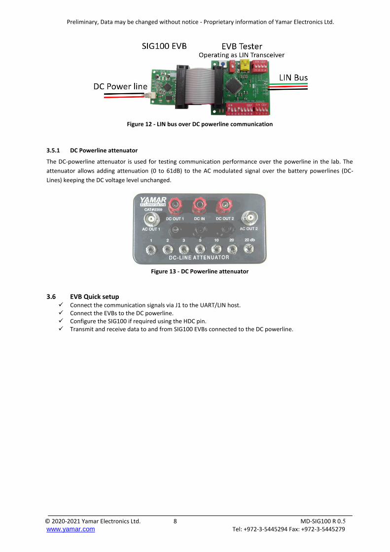
Figure 12 - LIN bus over DC powerline communication
3.5.1 DC Powerline attenuator
The DC-powerline attenuator is used for testing communication performance over the powerline in the lab. The
attenuator allows adding attenuation (0 to 61dB) to the AC modulated signal over the battery powerlines (DC-
Lines) keeping the DC voltage level unchanged.
Figure 13 - DC Powerline attenuator
3.6 EVB Quick setup Connect the communication signals via J1 to the UART/LIN host. Connect the EVBs to the DC powerline. Configure the SIG100 if required using the HDC pin. Transmit and receive data to and from SIG100 EVBs connected to the DC powerline.
Preliminary, Data may be changed without notice - Proprietary information of Yamar Electronics Ltd.
© 2020-2021 Yamar Electronics Ltd. 9 MD-SIG100 R 0.5 www.yamar.com Tel: +972-3-5445294 Fax: +972-3-5445279
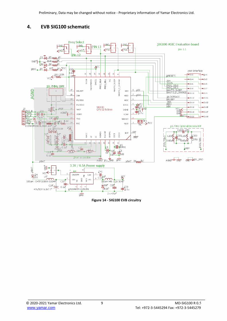
4. EVB SIG100 schematic
Figure 14 - SIG100 EVB circuitry

Preliminary, Data may be changed without notice - Proprietary information of Yamar Electronics Ltd.
© 2020-2021 Yamar Electronics Ltd. 10 MD-SIG100 R 0.5 www.yamar.com Tel: +972-3-5445294 Fax: +972-3-5445279
Revision History
Rev. Date Description
0.2 30/07/19 Initial version
0.3 03/09/19 Update schematics
0.4 15/11/20 Update Figure 14 to Rev 1.1.
0.5 14/01/21 Editing.