SiC Hybrid Modules for Decentralized Solar Inverters ...
11
SiC Hybrid Modules for Decentralized Solar Inverters Customer Presentation June 2020 6/9/2020
Transcript of SiC Hybrid Modules for Decentralized Solar Inverters ...
SiC Hybrid Modules for Decentralized Solar InvertersCustomer Presentation
June 2020
6/9/2020

Gel-filled Modules: Available Packages
Q1
with base
plate
Q2Q0 F2F1
1.2 mm press-fit pins
Solder pins
With TIM/no TIM
1.2 mm press-fit pins
1.6 mm press-fit pins
Solder pins
With TIM/no TIM
1.2 mm press-fit pins
Solder pins
With TIM/no TIM
1.2 mm press-fit pins
1.6mm press-fit pins
Solder pins
With TIM/no TIM
1.6 mm press-fit pins
Solder pins
With TIM/no TIM
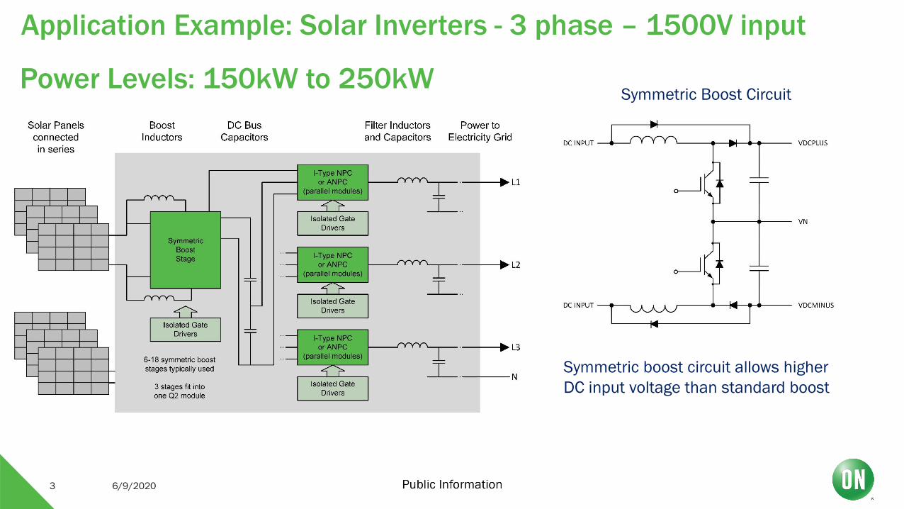
Application Example: Solar Inverters - 3 phase – 1500V input
6/9/20203
Symmetric Boost Circuit
Symmetric boost circuit allows higher
DC input voltage than standard boost
Power Levels: 150kW to 250kW
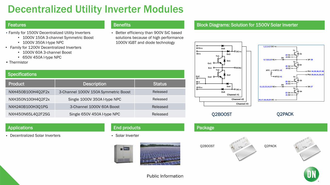
Features Benefits Block Diagrams: Solution for 1500V Solar Inverter
Specifications
Applications Package
• Solar Inverter
End products
• Decentralized Solar Inverters
Product Description Status
NXH450B100H4Q2F2x 3-Channel 1000V 150A Symmetric Boost Released
NXH350N100H4Q2F2x Single 1000V 350A I-type NPC Released
NXH240B100H3Q1PG 3-Channel 1000V 60A Boost Released
NXH450N65L4Q2F2SG Single 650V 450A I-type NPC Released
• Better efficiency than 900V SiC based
solutions because of high performance
1000V IGBT and diode technology
• Family for 1500V Decentralized Utility Inverters
• 1000V 150A 3-channel Symmetric Boost
• 1000V 350A I-type NPC
• Family for 1200V Decentralized Inverters
• 1000V 60A 3-channel Boost
• 650V 450A I-type NPC
• Thermistor
Decentralized Utility Inverter Modules
39 E2
D5
1,2,3,4,5 DC+
Ph1 34,35,36,37,38
16,17,18,19,20 DC-
NTC NTC1 42
NTC2 41
24 G1
T1
23 E1
D1
40 G2D2
21 E4
25 G3
26 E3
D3
22 G4D4
D6
T2
T3
T4
6,7,8,9,10 N1
11,12,13,14,15 N2
Ph2 29,30,31,32,33
SP 28
SN 27
Tx1
Tx2
Dx5
Dx3
Dx1
Dx2
DC+x
DCNx
Dx4
Dx6
DC-xBYS-x
IN-x
IN+x
BYS+x
Gx1
Gx2
Ex1
Ex2
Channel #1
Channel #2
Channel #3
Q2BOOST Q2PACK
Q2BOOST Q2PACK

Q2 3-Level Boost for 1500V System
5
Name Description Q'ty/Module
Tx1,Tx2 FS4 1000V/75A, High Speed 12
Dx1,Dx2 1600V/35A, Protection diode 6
Dx5,Dx6 1600V/35A, By-pass diode 6
Dx3,Dx4 1200V/10A, SiC Diode 18
NTC 22kohm, 5% (size 2012) 1
Tx1
Tx2
Dx5
Dx3
Dx1
Dx2
DC+x
DCNx
Dx4
Dx6
DC-xBYS-x
IN-x
IN+x
BYS+x
Gx1
Gx2
Ex1
Ex2
Channel #1
Channel #2
Channel #3

Loss Simulation at 29 kW per Channel
6
Boost Module Working Condition (per Channel)
Vin = 830V
Vout = 1170V, or 1300V
Iin = 35A per channel
Fsw = 16kHz (16~18 kHz)
Inductance = 500 uH
Heatsink = 90 degC
Result:
Power (kW) Vin (V) Vout (V) IG Rth-js Tj-IGBT (0C) Power loss-FWD (W) DI-Rth-js Tj-FWD (0C)
29.1 830 1170 0.5 111.3 52.9 0.7 125.4
29.1 830 1300 0.5 116.0 47.7 0.7 121.9
SiC is hotter than IGBT but the its temperature is well below Tjmax.

Q2 3-Level I-Type NPC for 1500V System
7
39 E2
D5
1,2,3,4,5 DC+
Ph1 34,35,36,37,38
16,17,18,19,20 DC-
NTC NTC1 42
NTC2 41
24 G1
T1
23 E1
D1
40 G2D2
21 E4
25 G3
26 E3
D3
22 G4D4
D6
T2
T3
T4
6,7,8,9,10 N1
11,12,13,14,15 N2
Ph2 29,30,31,32,33
SP 28
SN 27
Name Description Q'ty/Module
T1,T4 FS4 1000V/75A, High Speed 10
T2,T3 FS4 1000V/75A, Low Vce(sat) 8
D1,D2,D3,D4 1000V/75A, Diode 8
D5,D6 1200V/20A, SiC Diode 10
NTC 22kohm, 5% (size 2012) 1

120-150kW – Q2 INPC
2 6/9/2020
Higher output power can be achieved with higher output voltage
Outer IGBT is the hottest in most cases
Q4
D1
Q1
20,21 G1A/B
22 E1
11,13,14 BUSN1
1~4 BUS-
D49,10 G4A/B
8 E4
T1 33
T2 34
D6
D2
Q2
D3
Q3
23 G2
24 E2
39 G3
38 E3
16~19 BUS+
OUT1 25~28
OUT1 29~325,6,7 BUSN2
TP2 35, 37
TP1 40
D5
Vbus 850V, fsw 16.2kHz, Tsink 100, Rg_on/off 15Ω
Condition Vo[V] kVA PF Tj_Q1 [] Tj_D1 [] Tj_Q2 [] Tj_D5 []
1 230 100 1 129.6 100.0 125.1 114.2
2 230 110 1 133.6 100.0 128.5 116.0
3 230 111 0.9 132.1 100.5 129.8 118.1
4 230 125 0.8 135.2 101.5 136.0 123.0
5 230 121 1 138.3 100.0 132.4 118.1
6 230 122 0.9 136.5 100.3 133.9 120.5
7 230 137 0.8 140.3 101.3 141.1 126.0
8 230 132 1 143.2 100.0 136.5 120.2
9 230 132 0.9 140.7 100.4 137.7 122.6
10 230 150 0.8 145.6 101.4 146.4 129.2
11 288.7 126 1 132.1 100.0 125.1 109.1
12 288.7 139 1 136.5 100.0 128.5 110.2
13 288.7 140 0.9 134.7 100.6 129.8 112.7
14 288.7 158 0.8 138.1 101.7 135.9 117.1
15 311.8 136 1 133.2 100.0 125.1 107.1
16 311.8 150 1 137.7 100.0 128.5 107.9
17 311.8 152 0.9 135.9 100.6 129.9 110.6
18 311.8 170 0.8 139.4 101.9 136.0 114.9

Loss Simulation at 195kW, PF =0.8
9
Inverter Working Condition
VDC = 1170V
Vout L-L = 800Vrms
Fsw = 16kHz
Inductance = 83uH
Heatsink = 90 degC
Pf = 0.8
AC condition under simulation
IGBT-O : Out IGBT T1/T4
(Vce= 600V; Rg= 15 Ω; Vge= +15V/ -8V)

160 kW LVRT – Low Voltage Ride Through
10
LVRT limited the output power to 160kW. With Tjmax < 1350C (90%). LVRT voltage : 0 pu, ~ 150ms LVRT voltage : 0.2 pu, ~625 ms Comments
Phase Voltage, Vout Vout: 0V
(46.1V in practice**)Vout: 92V (0.2*461)
**At 0 pu, Vout =0V theoretically,
in practice Vout = 40V ~ 50V
(0.1pu)
Phase Current, Iout Lag 90 deg Lag 90 deg Magnitude: 121A (105%*In )
Phase angle: shift 900
P Q (reactive)
Result
Per DeviceLoss & Tj
Power Loss (W) ~up to 625ms max Tj ( 0C )IGBT-O 52.3 99.9IGBT-I 173.4 126.4
Diode-NP 132 133.6Protection Diode
D1,D4,D5,D6 9.24 96.9
LVRT Simulation

Thank You