SiC Band Gap Voltage Reference for Space Applications
77
University of Tennessee, Knoxville University of Tennessee, Knoxville TRACE: Tennessee Research and Creative TRACE: Tennessee Research and Creative Exchange Exchange Masters Theses Graduate School 5-2016 SiC Band Gap Voltage Reference for Space Applications SiC Band Gap Voltage Reference for Space Applications Charles Kenneth Roberts University of Tennessee - Knoxville, [email protected] Follow this and additional works at: https://trace.tennessee.edu/utk_gradthes Part of the Electrical and Electronics Commons Recommended Citation Recommended Citation Roberts, Charles Kenneth, "SiC Band Gap Voltage Reference for Space Applications. " Master's Thesis, University of Tennessee, 2016. https://trace.tennessee.edu/utk_gradthes/3802 This Thesis is brought to you for free and open access by the Graduate School at TRACE: Tennessee Research and Creative Exchange. It has been accepted for inclusion in Masters Theses by an authorized administrator of TRACE: Tennessee Research and Creative Exchange. For more information, please contact [email protected].
Transcript of SiC Band Gap Voltage Reference for Space Applications
University of Tennessee, Knoxville University of Tennessee, Knoxville
TRACE: Tennessee Research and Creative TRACE: Tennessee Research and Creative
Exchange Exchange
Masters Theses Graduate School
5-2016
SiC Band Gap Voltage Reference for Space Applications SiC Band Gap Voltage Reference for Space Applications
Charles Kenneth Roberts University of Tennessee - Knoxville, [email protected]
Follow this and additional works at: https://trace.tennessee.edu/utk_gradthes
Part of the Electrical and Electronics Commons
Recommended Citation Recommended Citation Roberts, Charles Kenneth, "SiC Band Gap Voltage Reference for Space Applications. " Master's Thesis, University of Tennessee, 2016. https://trace.tennessee.edu/utk_gradthes/3802
This Thesis is brought to you for free and open access by the Graduate School at TRACE: Tennessee Research and Creative Exchange. It has been accepted for inclusion in Masters Theses by an authorized administrator of TRACE: Tennessee Research and Creative Exchange. For more information, please contact [email protected].

To the Graduate Council:
I am submitting herewith a thesis written by Charles Kenneth Roberts entitled "SiC Band Gap
Voltage Reference for Space Applications." I have examined the final electronic copy of this
thesis for form and content and recommend that it be accepted in partial fulfillment of the
requirements for the degree of Master of Science, with a major in Electrical Engineering.
Benjamin Blalock, Major Professor
We have read this thesis and recommend its acceptance:
Syed Islam, Nicole MCFarlane
Accepted for the Council:
Carolyn R. Hodges
Vice Provost and Dean of the Graduate School
(Original signatures are on file with official student records.)

SiC Band Gap Voltage Reference
for Space Applications
A Thesis Presented for the
Master of Science
Degree
The University of Tennessee, Knoxville
Charles Kenneth Roberts
May 2016

ii
Copyright © 2016 by Charles Kenneth Roberts
All rights reserved.

iii
ACKNOWLEDGEMENTS
Thank you to Dr. Ben Blalock for your guidance and instruction, you saw
promise in me as a non-traditional student and without you I would not have
considered a graduate degree. I would like to thank Dr. R.E. Bodenheimer,
Michael C. Crabtree, and the Bodenheimer Foundation; without your gracious
financial support full time graduate school would not be possible for me. I would
like to thank Oak Ridge National Laboratory for giving me the time off of work to
peruse this degree.
I would like to thank Kyle Harris, Ben McCue, Jeff Dix, Ben Rohers, and
the ICASL team. We all have experience academic rigor together. I would like to
thank Jeff Patterson, Eric Breeding, Doug Curry, and Craig Deibele; your
mentorship and encouragement kept me moving forward.
And a special thanks to my wife Laura Roberts, she agreed to me
following this dream of an engineering education in 2011. It has been a long hard
5 years that has included many life changes and additions to our family, it has
been at a great cost to her and my boys for me to be away working and pursuing
this education. To Laura, its finally over, no more only seeing each other in
passing and handing off children.

iv
ABSTRACT
Electronics for space applications can experience wide temperature
swings depending on orientation towards stars and duty cycle of propulsion
systems. Energy on satellites primarily comes from radiological thermal
generators and / or solar panels. This requires space electronic applications to
be energy efficient and have high temperature tolerance. As a result, space
electronic systems use high efficiency SMPS [switching mode power supplies].
Currently, there exists SiC [silicon carbide] based electronics that is state
of the art for high temperature applications. Commercial manufacturers at this
time produce SiC Power MOSFETs [Metal Oxide Semiconductor Field Effect
Transistors], which are the switching element of the SMPS. Although many
commercial silicon SMPS controller IC’s [Integrated Circuits] are available on the
market at this time, there are no SiC SMPS controller IC’s. The scope of this
research project was sponsored by NASA which required the design, fabrication,
and testing of a single module SiC SMPS controller. A subcomponent of the
SMPS design was a BGR [bandgap voltage reference] for the controller. This
thesis will cover the theoretical basis of the BGR, the development methods and
challenges in the design of a SiC BGR; utilizing a commercial SiC process as a
major constraint in the designs. These constraints were partially tackled by using
topologies and techniques from the early days of n channel MOSFET based

v
electronics established in the1970’s. The basis of design was models provided
by the owner of the process. The BGR was designed with Kuijk BGR topology.
These devices are currently being produced in the microelectronics foundry
facility since the simulation analysis results have provided promising theoretical
data depicting a simulated temperature stability of 16.5 ppm / from 25-160 .

vi
TABLE OF CONTENTS
Chapter One: Introduction .......................................................................... 1
Motivation ............................................................................................... 1
Thesis Organization ................................................................................ 3
Chapter Two: Literature Review ................................................................. 5
Voltage References ................................................................................ 5
SiC Technology ...................................................................................... 7
Chapter Three: SiC BGR Design ............................................................... 9
Kuijk Band Gap Voltage Reference ........................................................ 9
Kuijk BGR Components in SiC ............................................................. 12
Diode-Resistor Network .................................................................... 14
Operational Amplifier......................................................................... 18
Start Up Circuit .................................................................................. 23
Kuijk BGR Design Process ................................................................... 28
Design Simulation Sweeps ............................................................... 29
Kuijk BGR Operational Simulation ........................................................ 31
Start Up ............................................................................................. 32
Stability ............................................................................................. 32
Temperature Sweep.......................................................................... 34
Kuijk BGR Schematic and Layout ......................................................... 36
vii
Chapter Four : SiC BGR Reference Test ................................................. 40
BGR Test Plan ...................................................................................... 40
BGR Test Schematic ............................................................................ 43
Chapter Five : Conclusions ...................................................................... 45
List of References .................................................................................... 46
Appendix .................................................................................................. 50
Vita ........................................................................................................... 65

viii
LIST OF TABLES
Table 3.1 : Op Amp Performance ....................................................................... 26
Table 3.2 : Stability Figures of Merit .................................................................... 34

ix
LIST OF FIGURES
Figure 3.1 : Kuijk BGR Topology......................................................................... 10
Figure 3.2 : Resistor Variation vs. Temperature ................................................. 19
Figure 3.3 : Diode Resistor Network ................................................................... 19
Figure 3.4 : Op Amp Schematic .......................................................................... 25
Figure 3.5 : Start Up With Highlighted Start Up Current Path ............................. 27
Figure 3.6: Parameterized BGR Circuit ............................................................... 30
Figure 3.7 : Dual Feedback Paths....................................................................... 33
Figure 3.8 : BGR Temperature Sweep Output .................................................... 37
Figure 3.9 : BGR IC Block Diagram .................................................................... 38
Figure 3.10 SiC BGR Layout .............................................................................. 39
Figure 4.1 : SiC BGR Test Circuit ....................................................................... 44
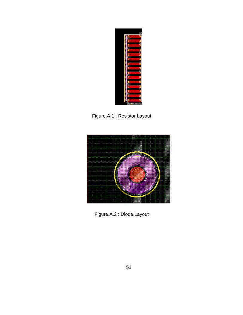
Figure.A.1 : Resistor Layout ............................................................................... 51
Figure.A.2 : Diode Layout ................................................................................... 51
Figure.A.3 : Diode 𝒅𝑰/𝒅𝑽 plot and I-V plot at 25 . ............................................ 52
Figure.A.4 : I-V plot Temperature Sweep, 25 - 300 . ....................................... 53
Figure.A.5 : Op Amp Open Loop Response at 𝟐𝟓 . ......................................... 54
Figure.A.6 : Op Amp Open Loop Response at 𝟑𝟎𝟎 . ....................................... 55
Figure.A.7 : BGR Start Up Circuit ....................................................................... 56
Figure.A.8 : SiC Diode IV Curves, 25 C .............................................................. 57

x
Figure.A.9 : Schematic of Diode NTC - PTC Temperature Sweep ..................... 58
Figure.A.10 : Diode NTC - PTC Temperature Sweep ......................................... 59
Figure.A.11 : R Parameter Sweep ...................................................................... 60
Figure.A.12 : 500ns Rise Time Start Up Simulation, Vout .................................... 61
Figure.A.13 : 1us Rise Time Start Up Simulation, Vout ........................................ 62
Figure.A.14 : 5us Rise Time Start Up Simulation, Vout ........................................ 63
Figure.A.15 : BGR Test Flow Chart .................................................................... 64

1
Chapter One:
Introduction
Motivation
The National Aeronautics and Space Administration’s (NASA) Next
Generation Deep Space missions will require high power solar electric propulsion
systems. NASA has proposed a High Temperature Boost (HTB) Power
Processing Unit (PPU). This unit uses controllers which are switch mode power
supplies. This design will generate the required voltages for the Hall Thruster and
required ancillary systems. This HTB-PPU will operate at higher operating
temperatures than current military specification electronics with, a junction
temperature of 160. This operating temperature is achievable by current Silicon
Carbide (SiC) extreme environment electronics [1].
The vacuum of space limits the mechanism of heat transfer primarily due
to radiation, except for conditioned environments on space craft. Temperature
controlled areas on space craft and satellites contribute to the overall mechanical
complexity. This form of complexity is additionally contributing to the overall
weight of the space system resulting in a major cost consumption. Another
2
limiting factor in space electronics is power consumption; energy on satellites
primarily comes from radiological thermal generators and / or solar panels, which
exhibit limited output power coupled with shortened lifespans. This requires
space electronic applications to be energy efficient and possess very low thermal
power dissipation.
Currently, one current state of the art technology associated with extreme
environment power electronics is SiC. At this time Cree, Micro Semi,
STMicroelectronics and other commercial manufacturers heavily produce SiC
Power MOSFETs. These transistors are the switching element of the SMPS that
still require a controller and driver to switch the transistor which is a current
drawback. Even though many commercial silicon SMPS integrated circuits (IC)
are available there is no commercial SiC SMPS controllers available on the
market. The SMPS IC provides a control loop to change the switching rate for the
switching transistor to modulate the output voltage and current. The project
scope of this thesis focused on the design of a single module SiC SMPS
Controller in collaboration with the University of Tennessee and the industrial
sponsor, NASA, which resulted in an additional supplemental design component
focused upon a bandgap voltage reference (BGR) for associated with the SiC
SMPS controller.
The SMPS topology in the HTB-PPU uses voltage as the variable
in the control loop and nonlinear carrier control. The control loop of the SMPS
3
compares a derived voltage from the output to the reference voltage generated
by the BGR. The purpose of a BGR is to provide a stable reference voltage
across the operating temperature and operating supply voltage. The HTB-PPU
switches the gate of the switching element of the SMPS with the control loop
maintaining the output voltage at a constant level.
SiC pn diodes have been used in proof of concept BGR designs with off
the shelf low temperature Silicon commercial operational amplifiers. These
designs only heat the diodes and do not expose any other components to
heating. [2] [3]. To meet the industrial sponsor design requirement of a single
module SiC SMPS one must implement the use of SiC based operational
amplifier combined with on chip passive components.
Thesis Organization
This thesis will discuss the design of a single chip Kuijk BGR in SiC
detailing the Kuijk topology BGR, impact of SiC as the semiconductor material in
the design, and the design steps for the BGR in SiC. Prefabrication simulations
were investigated to determine the ideal components to process the most
efficient SiC diode models. All design will illustrate and document the overall
process from conception to fabrication. An experimental test circuit and design
will assist with the testing method for the BGR.
4
Chapter 2 provides background information on the BGR and SiC devices
with corresponding design processes. Chapter 3 explains the analysis of the Kuijk
BGR design in SiC, presents the overall design process, and illustrates the
prefabrication simulations. Chapter 4 discusses the test plan and test card
implemented in the research project. Chapter 5 is a summary of the research
developed, designed, fabricated, and tested during the course of this project. The
main focus on this chapter is to discuss the research findings, criteria that met the
expectations of the project, and to conclude with future work.

5
Chapter Two:
Literature Review
This chapter will give a brief overview of the state of the art of voltage
references and SiC technology. It will cover voltage reference technologies that
were considered for this design, as well as a brief discussion of the state of the
art of SiC devices. The discussion of SiC devices will be limited to the properties
and devices associated with the band gap voltage reference.
Voltage References
The purpose of an voltage reference is to provide a stable voltage with
respect to temperature, supply voltage, loading, time and other parameters [4]
[5]. The current common reference technologies in production are band gap
references and buried Zener references [6]. Bandgap voltage references work by
balancing the temperature coefficients from a single forward biased diode 𝑉𝑑
against the differences in voltage of two forward biased diodes ∆𝑉𝑑. The 𝑉𝑑
voltage has a negative temperature coefficient and the ∆𝑉𝑑, which is proportional
to the thermal voltage, has a positive temperature coefficient [7] [5]. The negative

6
temperature coefficient diode forward voltage is approximately equal to the band
gap voltage of the semiconductor minus a coefficient of proportionality times the
temperature. Buried Zener references use the subsurface breakdown, of Zener
diodes to generate a temperature stable voltage reference [5]. Buried Zener
references are more accurate and temperature stable [6]. This project was
limited to bandgap voltage references due to the design criteria requiring the SiC
process. The SiC process that was used for this design does not have a Zener
diode which excluded the use of a buried Zener based design. An additional
topology investigated for the project uses difference in gate source voltage
between two matched NMOS transistors, one enhancement and one depletion,
to create a temperature stable voltage reference [8]. This topology was not used
because of threshold instability in SiC processes [9].
The band gap reference balances the 𝑉𝑑, diode forward voltage, and ∆𝑉𝑑,
diode thermal voltage by driving them to the same bias point and summing the
voltages through an error amplifier. The gains associated with the 𝑉𝑑 and ∆𝑉𝑑
terms are set by external resistive networks [7] [10]. These summed negative
and positive temperature coefficient voltages ideally yield a voltage with no
temperature coefficient. Because the diode forward voltage is dependent on the
saturation current of the diodes, this forces the output voltage of a band gap
voltage reference to have a voltage that is a parabolic function with temperature
7
and is in equation 2.1. T is temperature To is a reference temperature where the
temperature coefficient is zero, ɳ is a constant related to doping [10] [7].
𝑉𝑜 = 𝑉𝐺𝑂 + (ɳ − 1)𝑘𝑇𝑜
𝑞−
1
2(ɳ − 1)
𝑘𝑇𝑜
𝑞(
∆𝑇
𝑇𝑜)
2
Equation 2.1
This curvature is present in all band gap voltage reference designs. BGR
circuits tend to be more positive temperature coefficient in nature at lower
temperatures and negative temperature coefficient in nature at high temperatures
[11]. This curvature can be removed by higher order curvature compensation
techniques [4] This was not attempted in this design due to device modeling
issues and a lack of a PMOS device.
SiC Technology
Silicon Carbide is a wide band gap semiconductor material, it has a high
electric breakdown field, high electron saturated drift velocity, high melting point
and high thermal conductivity [12]. This makes it an ideal semiconductor for high
temperature applications. The operation of a high temperature semiconductor is
dependent on its bandgap, intrinsic carrier concentration, carrier mobility. The
limitation on operation of a semiconductor at high temperature can be thought of
in terms of leakage current, as the leakage current increases the device
transitions for being a semiconductor to a conductor. The leakage current is
proportional to the square of the intrinsic carrier concentration and is shown in

8
equation 2.2 below. Eg is the band gap, ni is the intrinsic carrier concentration ,NC
and NV are the density of states of the conduction and valence band, T is
temperature and k is Boltzmann’s constant [13].
𝐼𝑂 ∝ 𝑛𝑖2 = (𝑁𝐶𝑁𝑉)𝑒(
−𝐸𝑔
𝑘𝑇) Equation 2.2
The leakage current is from carriers being thermally excited to the
conduction and valence bands, SiC’s low intrinsic carrier concentration and low
temperature dependence of intrinsic carriers allow it to perform as a
semiconductor at high temperature. SiC has similar process chemistry to Si,
PMOS SiC MOSFETs have poor performance due to doping issues. [14]
SiC n-channel MOSFET’s have been used to design a high temperature
operational amplifier that operates at a temperature of up to 350 º C
Wth an open loop gain of greater than 40 dB [15]. SiC power transistors are
available commercially from multiple manufactures, these are n channel power
devices.
A proof of concept of a SiC p-n and Shockley diode BGR have been
designed and fabricated by other institutions. These are card level
implementations using an Si operational amplifier, only the diodes were exposed
to high heat. [2] [3]. Using a SiC MESFET, second order temperature
compensation was achieved in the Shockley diode BGR circuit [3].
9
Chapter Three:
SiC BGR Design
Kuijk Band Gap Voltage Reference
The Kuijk band gap voltage reference is a self-biased first order
compensated voltage reference [4] [5]. The circuit element that generates the
positive temperature coefficient and negative temperature coefficient can be a
diode as opposed to the Brokaw band gap reference that requires a bipolar
junction transistor. Additionally, this design also does not require a PMOS
transistor as in the case of the beta multiplier BGR since the output of the BGR is
used to bias the resistor diode network directly. The 4H-SiC process that was
used to design and implement the BGR in this research has NMOS transistors,
resistors, capacitors, and diodes. This limited set of devices made the Kuijk an
excellent fit. The Kuijk BGR consists of an op amp, resistor network, diodes, and
start up circuit. The figure below shows the BGR topology while omitting the
startup circuit.
The principle of operation of the Kuijk BGR is the same as other BGR
circuits, the forward biased diode generates a negative temperature coefficient
(NTC) voltage, VD diode forward voltage, and the difference between the two
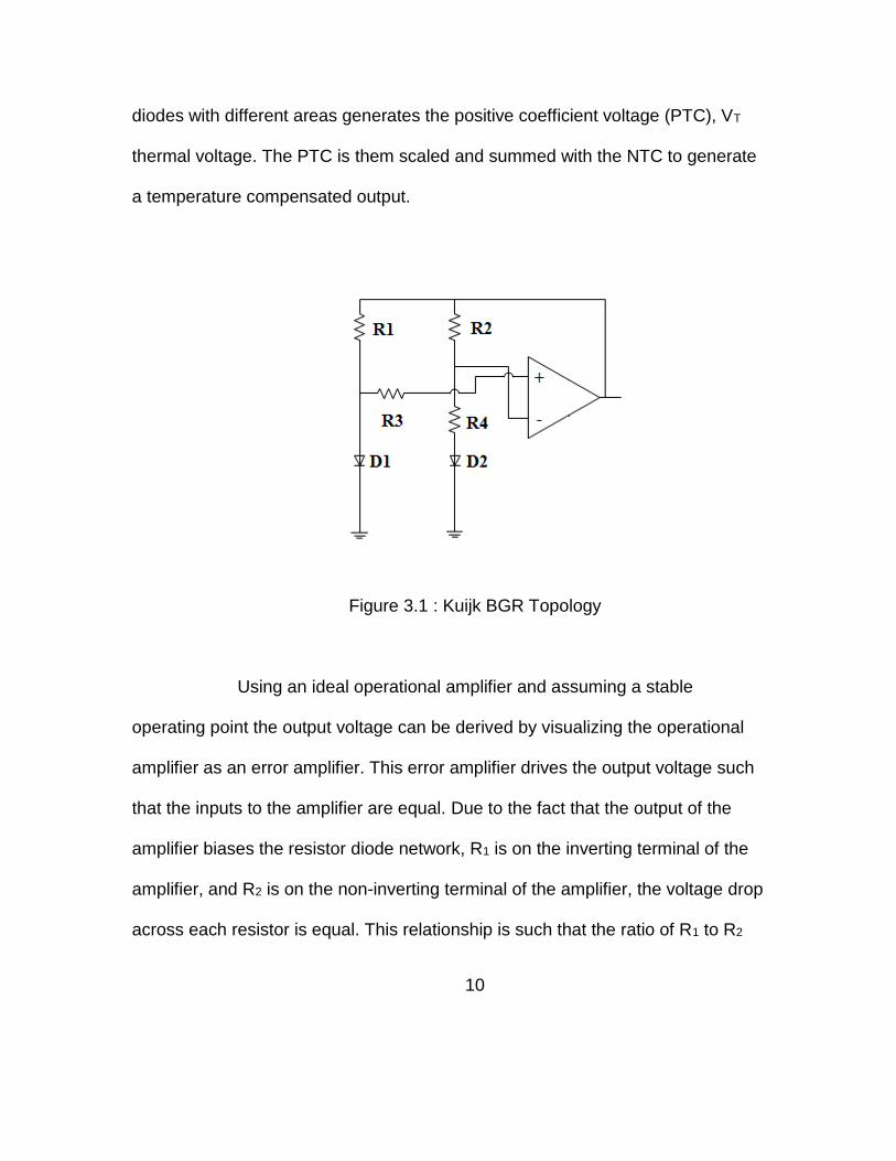
10
diodes with different areas generates the positive coefficient voltage (PTC), VT
thermal voltage. The PTC is them scaled and summed with the NTC to generate
a temperature compensated output.
Figure 3.1 : Kuijk BGR Topology
Using an ideal operational amplifier and assuming a stable
operating point the output voltage can be derived by visualizing the operational
amplifier as an error amplifier. This error amplifier drives the output voltage such
that the inputs to the amplifier are equal. Due to the fact that the output of the
amplifier biases the resistor diode network, R1 is on the inverting terminal of the
amplifier, and R2 is on the non-inverting terminal of the amplifier, the voltage drop
across each resistor is equal. This relationship is such that the ratio of R1 to R2

11
sets the ratio of the currents through the diodes D1 and D2. The relationship
between the current through a diode and the diode voltage is expressed by
equation 3.1, where Vd is the diode forward voltage, VT is the thermal voltage, Id
is the diode forward current, and Is is the saturation current of the diode.
𝑉𝑑 = 𝑉𝑇 ln(𝐼𝑑
𝐼𝑆) Equation 3.1
Under the ideal operational amplifier assumption there is no current
through resistor R3 and the voltage across R4 is the ΔVd = Vd1 – Vd2. Substituting
Equation 3.1 and the resistor current divider into this relationship we arrive at the
following, equation 3.2.
𝑉𝑅4 = ∆𝑉𝑑 = 𝑉𝑑1 − 𝑉𝑑2 = 𝑉𝑇 ln(𝑅2
𝑅1
𝐼𝑆2
𝐼𝑠1) Equation 3.2
Since the circuit elements R4 and R2 are in series the currents are the
same we can use Ohm’s Law and equation 3.2 to derive to the following equation
3.3.
𝑉𝑅2 = 𝑅2𝐼2 = 𝑅2𝑉𝑅4
𝑅4=
𝑅2
𝑅4𝑉𝑇 ln(
𝑅2
𝑅1
𝐼𝑆2
𝐼𝑠1) Equation 3.3
With the output of the BGR biasing the series components R2, R4, and D2,
the output voltage of the BGR via Kirchhoff's Voltage Law is expressed by
equation 3.4.
𝑉𝑂𝑈𝑇 = 𝑉𝑅2 + 𝑉𝑅4 + 𝑉𝑑2 = 𝑉𝑑2 + 𝑉𝑇 ln(𝑅2
𝑅1
𝐼𝑆2
𝐼𝑠1) +
𝑅2
𝑅4𝑉𝑇 ln(
𝑅2
𝑅1
𝐼𝑆2
𝐼𝑠1) =
𝑉𝑂𝑈𝑇 = 𝑉𝑑2 + 𝑉𝑇 ln(𝑅2
𝑅1
𝐼𝑆2
𝐼𝑠1) (1 +
𝑅2
𝑅4 ) Equation 3.4

12
This derivation shows that the output is the sum of the diode forward
voltage, Vd2, and a scaled thermal voltage, VT. The NTC voltage is Vd2 and the
PTC voltage is VT. The scaling factor is (1 +𝑅2
𝑅4 ) ln(
𝑅2
𝑅1
𝐼𝑆2
𝐼𝑠1) . The (1 +
𝑅2
𝑅4 ) term is
the non-inverting gain of the amplifier, and the other term, ln(𝑅2
𝑅1
𝐼𝑆2
𝐼𝑠1) , represents
the difference in current densities of the D1 and D2. This difference in current
densities is set by two factors. The ratio of resistance R2 to R1 divides the current
between the two diodes and the ratio saturation currents Is2 to Is1 is proportional
to the area of the p-n junction. In the proprietary 4H-SiC process used for this
design a diode of a fixed size that was characterized and modeled in SPCIE. To
increase the saturation current of the diode you must increase the area of the p-n
junction of the diode, to do this with the fixed sized diode multiple diodes are
placed in parallel for D2 to increase the effective area of the D2 p-n junction. By
using a multiple of the unit diode we can express the ratio as (n:1) = k where n is
the number of diodes. The output can then be expressed as equation 3.5.
𝑉𝑂𝑈𝑇 = 𝑉𝑑2 + 𝑉𝑇 ln(𝑅2
𝑅1𝑘) (1 +
𝑅2
𝑅4 ) Equation 3.5
Kuijk BGR Components in SiC
The previous derivation of the output voltage of the BGR uses the ideal
operational amplifier as the error amplifier. This neglects the contributions of
13
limited gain, offset voltages, and offset currents while neglecting contributions
from temperature dependence in these terms.
SiC is a wide bandgap semiconductor that has an intrinsic carrier
concentration that stays in the regime of a semiconductor at high temperatures.
The intrinsic carrier concentration of undoped 4H-SiC at 25 is 10−6, and at
300 is 104 (citations). This low intrinsic carrier concentration provides for high
temperature operation but also lowers the gain of the MOSFET device, especially
at room temperature. PMOS technology in this proprietary 4H-SiC process is not
mature enough for use in design, the devices have not been adequately
modeled, suffer exceptionally low gain, and exhibit threshold voltage instability.
The NMOS devices are better modeled but still have low gain in comparison to Si
devices and as well as threshold voltage stability issues. This low gain and
restriction in device selection impacts the practical implementation of a SiC BGR.
The proprietary process used for this design introduced complexities by
using different modeling methods for the resistors and transistors versus the
diode. This made it difficult to simulate the overall design and modeling the
temperature depended effects related to both the op amp and resistors
simultaneously with the diodes. The challenges and implications of the SiC
devices on the BGR performance will be discussed in the next subsections.
14
Diode-Resistor Network
The diode resistor network is the portion of the BGR circuit that generates
the PTC thermal voltage and the NTC diode forward voltage. Additional resistors
set the gain of the PTC thermal voltage and the current division between the two
diodes in the design. This network consists of a resistor in series with D1 and two
resistors in series with D2 that provide a feedback network for the operational
amplifier (op-amp) as illustrated in Figure 3.3. A resistor diode network can be
used to create a BGR without any amplifier, but this requires a high rail voltage
for multiple diode drops which provides no resistive load capability [1].
The resistors in the process that were use are an n-type channel on a p-
type epitaxial layer, the channel was doped at 5 × 10¹⁵ 𝑐𝑚−3 via nitrogen ion
implantation [2]. Each resistor is surrounded by isolation well, as illustrated in
figure A.1 (see Appendix). This np+ resistor has with the smallest temperature
coefficient in the process with, a negative temperature coefficient of
approximately −280 𝑝𝑝𝑚
the test circuit and simulation results for the resistors
are shown in figure 3.2. The np+ resistor was selected for the small temperature
coefficient it possesses. The resistor models provided by the process owner are
temperature binned, the resistor performance is not characterized across the
entire temperature range but only at 25° C and 300°C.
The BGR circuit is sensitive to variation of resistance in terms of ratio to
other resistors and absolute value. The variation in absolute value of the resistors

15
impacts the magnitude of the currents flowing through D1 and D2, where the
current is set by the magnitude of the resistors and selected to place the Q point
of the diode in a region with little variation of forward voltage with respect to
forward current, moving the operating current out of this region will move the
BGR output from the bandgap voltage and from being temperature stable.
The variation of the relative resistor ratios impacts the output voltage in
two ways; (1) by changing the ratio of R2/R1 it changes the current division
between D1 and D2, (2) by changing the ratio of R2/R4 it changes the gain of the
thermal voltage term. The ratio error for R2 / R1 has a smaller impact on the
overall error due to the fact it is compressed by the ln() function. The ratio error
for (1 +𝑅2
𝑅4 ) has the largest impact as it is the gain for the VT term and also is the
gain for the total offset voltage which will be discussed in the next section. The
variation in the BGR output voltage, ∆𝑉𝑂𝑈𝑇,𝑅, is expressed by equation 3.6.
Where 𝜀𝑟the error of the ratio between resistor values, R is is component resistor
value, and VT is the thermal voltage.
∆𝑉𝑂𝑈𝑇,𝑅 = 𝑉𝑇 ln(𝑅2
𝑅1𝑘(1 + 𝜀𝑟)) (1 +
𝑅2
𝑅4 ) (1 + 𝜀𝑟) Equation 3.6
The relative variation of resistor values can be mitigated via layout
techniques. Resistors can be placed in a common centroid, where the resistor
placement on the IC has an average distance between each resistor in the
resistor diode resistor network is the same. This placement will have an
alternating patter of resistors and that will force the process variation to impact all

16
resistors equally. This was not implemented in this process as it only has a single
metal routing layer, the other layer available for routing was polysilicon. Routing
that would require a crossing of metal layers would need polysilicon routing, this
would introduce stray resistances that could overwhelm any benefit from the
common centroid placement. An additional technique investigated is the use of
guard rings around resistors; this was inherent to the process as the fabrication
of the resistors required an individual well. Another approach studied involved
the use of dummy elements that are placed around the actual resistors in use in
the design; this reduces edge effects from the fabrication process. This was not
utilized on this design as the process holder did not have data to support any
benefits in accuracy from use of dummy resistors.
The SiC process has a p-n junction diode of fixed dimensions. This diode
has a continuous temperature model from 25° C to 300°C, the operating
temperature of the diode is set by holding the simulator temperature constant
and sweeping a variable in the model. In Figure A.4 one can see a temperature
sweep of the diode model showing its performance. This is different than the
models for the transistors and resistors, which have models that must be
changed to simulate at two different temperatures. The process holder has
modeled the diode across current ranges of 1 nA to 1 µA and 100’s of µA, the
rest of the data is interpolated. The diode model has discontinuities where the
measured data is interpolated. This caused difficulty in the startup simulations as
17
the inflection points become additional stable self-biasing points. This diode was
large in area as it was designed to be a power component, the diode is 120µm
wide and is illustrated in the appendix in Figure.A.2 : Diode Layout.
Aside from difficulties introduced from immature diode models the diode
can create errors in the output based on variation of the diode area ration. This
error is represented by 𝜀𝐷 the percent variation in diode ratio area. The log of the
ratio of emitter area of D1 to D2 is part of the VT positive temperature coefficient
voltage term, where this term is generated by taking the difference of the two
diode VD forward voltages. The impact of the error of diode area ratios on output
is show in equation 3.7.
∆𝑉𝑂𝑈𝑇,𝐷 = 𝑉𝑇 ln(𝑅2
𝑅1𝑘(1 + 𝜀𝐷)) Equation 3.7
Diode area errors are commonly mitigated by using common centroid
techniques to minimize variations from the process. The SiC process had limited
routing layers which prevented true common centroid without adding polysilicon
jumpers to cross the single metal routing layer. The addition of polysilicon
jumpers would add stray resistances to the circuit, changing the bias point of the
diodes and adding a temperature dependent resistor. This particular approach
allowed the diode placement to be as compact as possible without routing on the
polysilicon layer. This was done by staggering the diodes and placing them as
close as possible while maintaining a minimal area to route between them. This
18
was not an ideal approach but provided the best protection against process
variation while working within the limited routing layers of the SiC process
Operational Amplifier
The operational amplifier utilized for the BGR was designed by Dr. Ben
McCue for use in the SMPS design. The mixed-mode op-amp is a self-biased
design that provides bias-point temperature tracking. By utilizing a depletion-
mode NMOS input stage an input common-mode range of 0 to 7.6 V is achieved.
No resistors are used in this design as all loads in this op-amp are depletion
mode devices.
The low-gain differential input pair feeds a floating voltage source cascode
structure, Stage 1 of Figure 3.4. The input stage is followed by a temperature-
tracking, high-gain common source stage, Stage 2 of Figure 3.4. A low-gain,
low-impedance output stage is buffers the op-amp output and restricts the bias
point movement of the high-gain, common-source stage, Stage 3 of Figure 3.4.
Temperature-tracking compensation ensures stable operation over temperature.
The NMOS devices that are used in the Op Amp in this process are
modeled via temperature bins. A SPICE model exists for the NMOS devices
operating at a room temperature (RT) and at high temperature (HT). The room
temperature is at 25° C while the high temperature is at 300°C where; both
models are operated at a simulated temperature of 25° C. This is opposed to the
diode temperature model which is continuous from 25° C to 300°C. This

19
Figure 3.2 : Resistor Variation vs. Temperature
Figure 3.3 : Diode Resistor Network
20
difference in modeling made it impractical to model the contribution of the
op amp induced errors across the entire temperature range in the BGR
The function of the operational amplifier in this design acts as an error
amplifier by providing feedback to force the input terminals to the amplifier to
have the same voltage, as in equation 3.7 [12]. Where Vo is the output of the
amplifier, Ao is the DC gain, V+ is the voltage at the non-inverting terminal, V- is
the inverting terminal voltage, and 𝜀𝑂𝐴 is the error from DC gain. This effectively
forces the same currents through the diode pairs. The amplifier adversely
impacts BGR performance predominantly via DC errors. It occurs through two
mechanisms; (1) DC gain and (2) total voltage offset.
∆𝑉𝑂/𝐴𝑂 = (𝑉+ − 𝑉−) = 𝜀𝑂𝐴 Equation 3.7
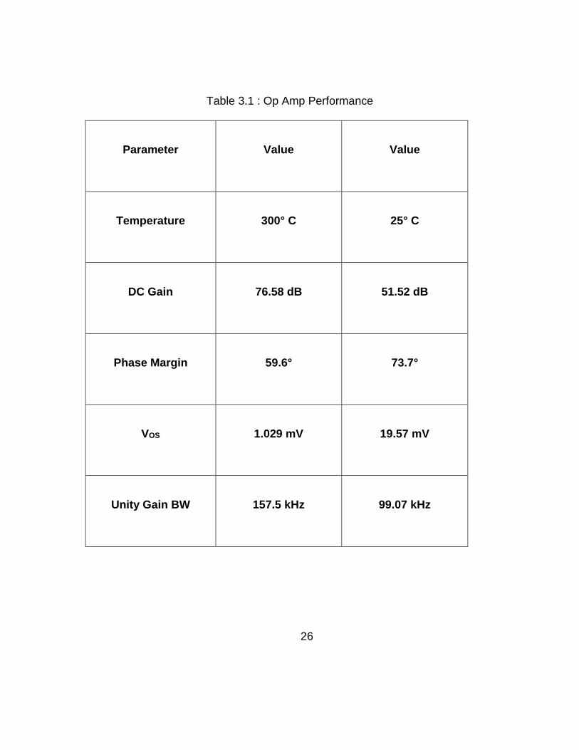
The Ao or open loop DC gain of the operational amplifier is driven by the
gm of the SiC devices. Typical gain of a two stage Si CMOS op amp is 1000 V/V
[3], while this SiC NMOS op amp has a room temperature gain of approximately
300 V/V to a high temperature gain of approximately 6000 V/V. The low intrinsic
carrier concentration of the SiC devices at room temperature creates low gm and
low room temperature gain. The open loop gain for 25° C is shown in Figure.A.5
: Op Amp Open Loop Response at 𝟐𝟓 .(see Appendix) and for the 300° C case
for Figure.A.6 : Op Amp Open Loop Response at 𝟑𝟎𝟎 .(see Appendix).
The error 𝜀𝑂𝐴 that is contributed by low DC gain can be referred back to
the non inverting input of the operational amplifier. The 𝜀𝑂𝐴 term sums with the
21
error from fixed voltage offset VOS, and temperature dependent voltage offset drift
∆𝑇𝑉𝑂𝑠
∆𝑇, to create VOST, the total offset depicted in equation 3.8 [13].
𝑉𝑂𝑆𝑇 = 𝑉𝑂𝑆 + 𝜀𝑂𝐴 + 𝑇∆𝑉𝑂𝑆
∆𝑇 Equation 3.8
Then by adding this VOST source to the BGR circuit in Topology and
solving for VOUT we arrive at equation 3.9. It demonstrates that the VOST error
voltage has the same gain as the 𝑉𝑇 ln(𝑅2
𝑅1𝑘) term.
𝑉𝑂𝑈𝑇 = 𝑉𝑑2 + 𝑉𝑇 ln(𝑅2
𝑅1𝑘) (1 +
𝑅2
𝑅4 ) + (1 +
𝑅2
𝑅4 ) 𝑉𝑂𝑆𝑇 Equation 3.9
The offset voltage and temperature dependent offset voltages come from
two different sources. The offset voltage is that is fixed comes from the mismatch
of the input differential pair structure and fabrication process. These are normally
addressed via layout techniques such as interdigitating, common centroid, and
interconnect matching [3]. In the SiC process that was used for this BGR there
was only one metal routing layer available, and the transistors were relatively
large to account for low gm. The lack of additional routing layers made common
centroid techniques not feasible, and the large transistor size made dummy
transistors not as practical.
The temperature dependent offset term is a function of temperature
dependent on variation of threshold voltage. For a MOSFET differential input
structure as in stage 1 of figure 3.4 VOS is the difference between the VGS of the
differential input structure transistors, VOS = (VTH1 – VTH2). The definition for VGS of
22
a MOSFET is shown in equation 3.10, where VTH is the threshold voltage, ID is the
drain current, µ is the carrier effective mobility, COX is the oxide capacitance, L is
transistor length, and W is transistor width.
𝑉𝐺𝑆 = 𝑉𝑇𝐻 + (2𝐼𝐷
𝜇 𝐶𝑂𝑋∙
𝐿
𝑊)
1
2 Equation 3.10
Using Equation 3.10, the previous definition for VOS, assuming matching
between the differential pair transistors with, equal currents we arrive at VOS
being the difference between the threshold voltages for the two input differential
pair transistors. For SiC MOSFETS VTH Threshold voltage is the most significant
parameter in the study of temperature dependence of MOSFET characteristics
[14]The temperature dependence of VTH is what creates the temperature
dependent VOS term, ∆𝑉𝑂𝑠
∆𝑇. This temperature dependent term can dominate the
PTC voltage generated by the thermal voltage, VT [4]. [3]. Table 3.1 shows the
two VOS and other parameters at the temperature bins given by the models
This dominating VOS term can be addressed in multiple ways. In
processes with bipolar junction transistors as the forward voltage, NTC voltage
and thermal voltage, PTC voltage, generators the transistors can be cascaded to
increase ∆𝑉𝐵𝐸 = 𝑉𝑇 which increases the thermal voltage [3]. This was not
possible in this process due to the fact that the source of the PTC and NTC
voltages are diodes. The design from the Kuijk paper used multiple diode
connected BJTs in series and a preamplifier to increase the VT term and minimize

23
the impact of ∆𝑉𝑂𝑠
∆𝑇 [5]. This approach was not taken in this design for two
reasons: (1) the Kuijk design had BJT devices available to create a preamplifier
which would minimize the ∆𝑉𝑂𝑠
∆𝑇 from the preamplifier, (2) and the BGR was
designed to be compact enough to fit on a single chip with the additional SMPS
components. Adding additional diodes in series would have made the design
unable to fit on a single SMPS IC. As the goals of the SMPS design shifted from
a single IC to a multi-chip module this was less of an issue, but the BGR was
designed with the goal of fitting on a single IC with the remainder of the SMPS.
Another technique investigated to increase VT is to increase the current
through the diode with the smaller transistor and while decreasing the current
through the larger transistor. This changes the I2 and I1 term in the ln(𝐼2
𝐼1
𝐼𝑆2
𝐼𝑠1) term
inside the VT gain [4]. This technique was not used in this design since the ratios
are defined by resistors and the absolute accuracy of these resistors was
uncertain for the process; Additionally the difference between the current ratios is
compressed by the ln() function diminishing the return of changing the current
ratio.
Start Up Circuit
The Kuijk BGR is a self-biased design due to the fact that the output of the BGR
supplies the bias for the diodes that generate the PTC and NTC voltages. The
operational amplifier drives its output such that the differences between the

24
inverting and non-inverting terminals of the operational amplifier are zero. This
occurs at bias levels of the diode, when no current is flowing through the diodes
and the voltages at both terminals of the operational amplifier, and when there is
a current flowing through both diodes such that the voltage at each operational
amplifier is equal. The latter is the case when the output of the voltage reference
is the temperature stable band gap voltage, the former case has no output at all.
In some situations, noise generate from the operational amplifier or resistor
components can be enough to drive the BGR out of the zero current bias state,
but to ensure consistent start up an external start up circuit must be provided.
The SiC process used for the BGR is an NMOS only process. This lack of
PMOS transistor prevented the use of start-up circuits which are common in
CMOS design. This forced the author to look at start up circuit topologies that are
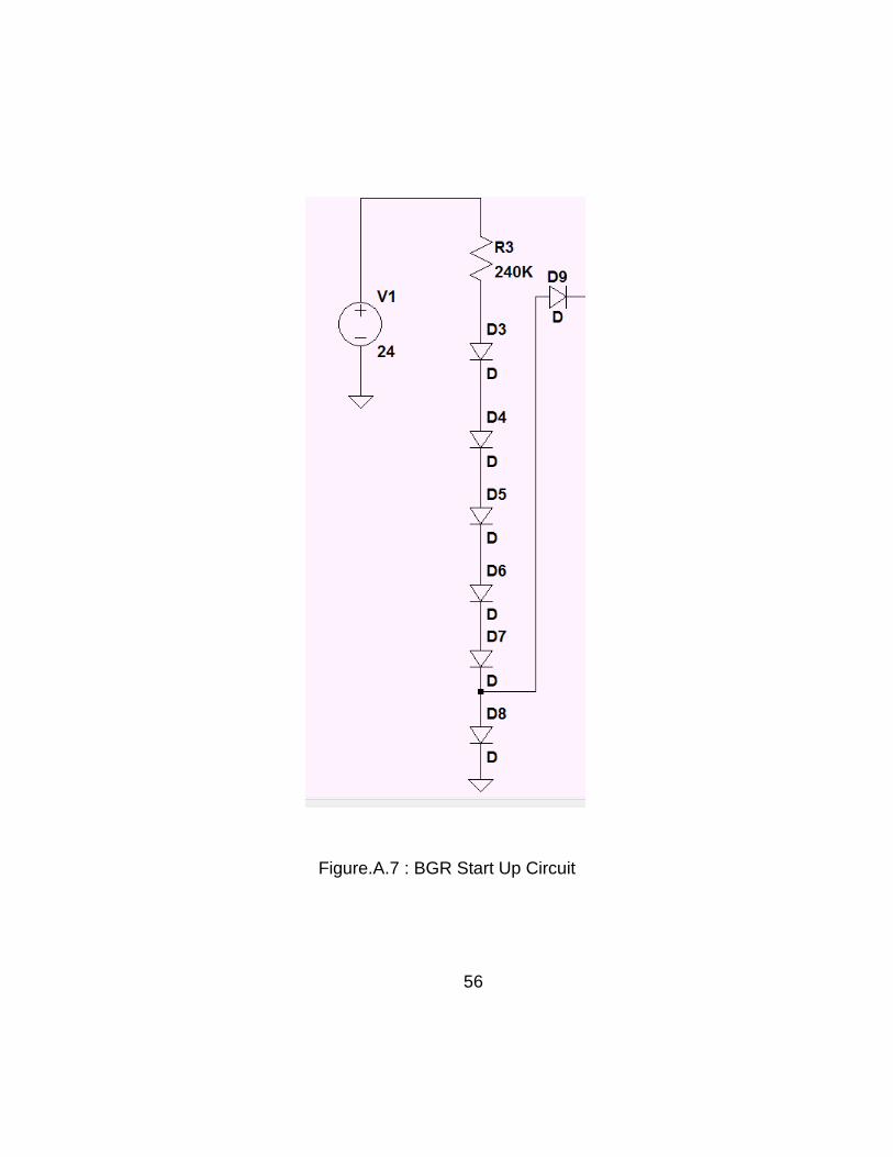
common in BJT based designs. The topology selected uses the SiC diodes and
shown in figure A.7 (see Appendix). The topology is from [3]. The series of 6
didoes provides a fixed voltage for the diode that connects to the BGR output.
When the BGR circuit is in the zero current state the diode D3 is forward biased,
allowing current to flow into the resistor diode network of the BGR. Once the
BGR circuit reaches its operating point the diode D3 is no longer forward biased
and no longer conducts current. Figure 3.5 shows the path of the current in the
startup circuit and the voltages across D3 when the BGR is at its operating point.
The series resistor was chosen to limit the current through the series diodes and

25
Figure 3.4 : Op Amp Schematic
26
Table 3.1 : Op Amp Performance
Parameter Value Value
Temperature 300° C 25° C
DC Gain 76.58 dB 51.52 dB
Phase Margin 59.6° 73.7°
VOS 1.029 mV 19.57 mV
Unity Gain BW 157.5 kHz 99.07 kHz

27
Figure 3.5 : Start Up With Highlighted Start Up Current Path

28
Kuijk BGR Design Process
Using the operational amplifier from the SMPS design and the fixed size
diode from the SiC process, the design process for the BGR consists of
component value selection for the resistors R1, R2, R3, R4, and the number of
diodes in parallel for D2. The ratio of the resistance values are set gain of the VT,
thermal voltage, the current division between didoes D1 and D2 and the stability
of the design. The absolute values of R1, R2, and R4 limit the currents being
forced through D1 and D2.
The values of are selected by a parameterized equation that zeros out the
sum of the temperature coefficients of the Vd and VT terms. The equation is
based off of the ideal output equation for the BGR and the assumption that R2
and R1 have the same value. The current through both diodes is held the same
because of the small benefit to the ∆𝑉𝑑 = 𝑉𝑇 ln(𝑅2
𝑅1
𝐼𝑆2
𝐼𝑠1) term and lack of consistent
diode model across current range. The parameterized design equation is derived
below as Equation 3.11, the schematic showing the parameters is Figure 3.6 see
below.
.
𝑉𝑂𝑈𝑇 = 𝑉𝑑2 + 𝑉𝑇𝑀, 𝑙𝑒𝑡 𝑀 = ln(𝑅2
𝑅1𝐾) (1 +
𝑅2
𝑅4 )

29
𝜕𝑉𝑂𝑈𝑇
𝜕𝑇=
𝜕𝑉𝑑2
𝜕𝑇+
𝜕𝑉𝑇
𝜕𝑇𝑀
𝑀 = ln(𝛼𝑅
𝛼𝑅𝐾) (1 +
𝛼𝑅
𝑅 )
𝑀 = ln(𝐾) (1 + 𝛼 ) Equation 3.11
Design Simulation Sweeps
The parameterized equation 3.11 requires the temperature dependence of
the VT and VD voltages to calculate the required resistor ratio values. These
temperature dependences are found via simulation of the process owner. A
current voltage sweep of the VD diode and VT diode array were also performed to
ensure that the absolute value of the resistors would put the diodes in a suitable
and modeled operating point.
The multiplier K for the diodes was selected to be 8, this is because the
approximate value of the ln(8) is 2. Using this multiplier an IV sweep of the single
VD diode and VT 8 diode parallel pair was generated. Based off the process
holder’s information for measured portion of the diode IV curve and the current
value that would give least variation in voltage a current of 9 µA was selected as
a target value. The schematic is Figure A.9 (see Appendix) and the IV plots are
on Figure A.10 (see Appendix). These temperature simulations are critical to the
design and must also be repeated as a measurement to ensure the resistor
values are correct. Variation in the temperature behavior of the diode model will
negatively impact the temperature behavior of the designed circuit.

30
Figure 3.6: Parameterized BGR Circuit

31
Based upon the target current value from the I-V sweep a temperature vs
voltage sweep was performed on the single and eight diode pair with the 9 µA
target current forced through them. These plots were used to find the
temperature dependence of the forward voltage of diode D1 and the temperature
dependence of diode D2 , the difference between these two voltages were taken
to arrive at the temperature dependence of the VT voltage times the factor of 2
from the 8 diodes in parallel. Using these values and equation 3.11 the value of α
was found to be 6.
Using the K value of 8 and α value of 6 the circuit in figure 3.6 was
simulated at 25C to find the output voltage. The value of R was swept from 4 kΩ
to 14kΩ. The value of R was selected that gave the closest value to the band gap
voltage of 4H Silicon Carbide. This value is 10kΩ. The resistor values for R1 and
R2 are 60 kΩ, while R3 and R4 are 10kΩ.
Kuijk BGR Operational Simulation
After running simulations to optimize the values of resistors in the design
and the number of diodes, simulations were performed to verify start up and
operation. Due to the fact the BGR is a self-biased design it is sensitive to start
up transients. Analysis was also performed to simulate frequency response of the
dual feedback paths of the BGR and verify stable operation in the time domain.
The BGR was also simulated for temperature accuracy.
32
Start Up
The voltage rails are the only external inputs into the feedback system of
the BGR. By running transient simulations of voltage rails at various rise times
you measure the step response of the BGR system. This is a time domain
measure of the stability of the system.
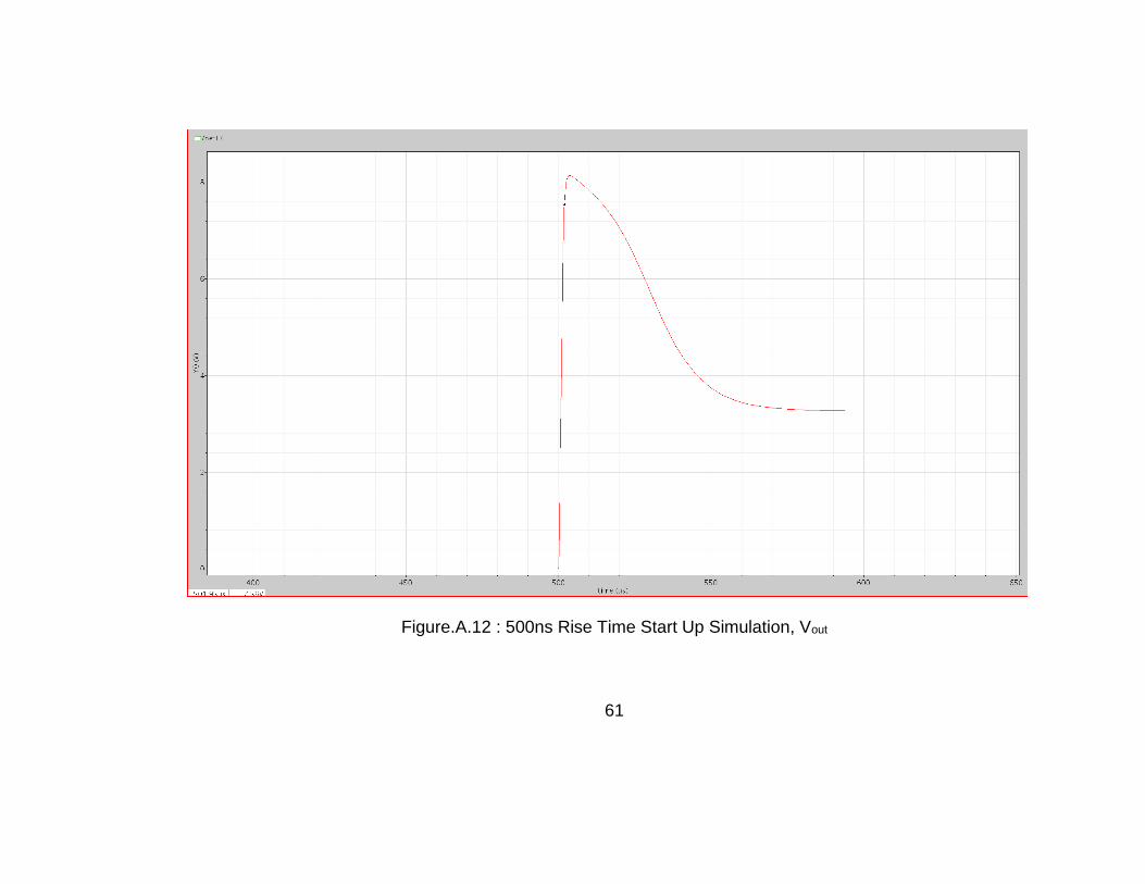
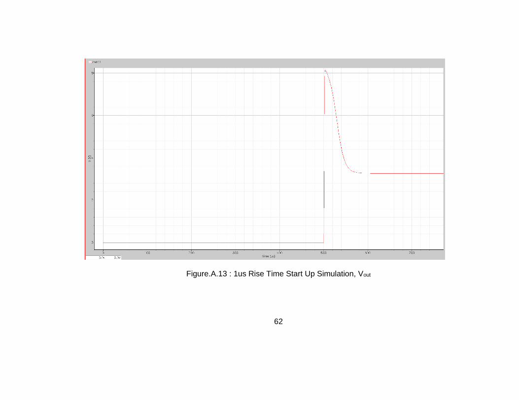
The BGR was simulated with a 24V supply voltage. The cases of 500ns,
1µs, and 2µs rise times were simulated. In all cases the system had an initial
overshoot and settled to the operating point of the BGR without oscillating or
ringing for multiple cycles. The simulation plots are in the appendix as figures
A.12, A.13, and A.14.
Stability
The frequency domain stability response of the BGR circuit can be found
by conceptualizing the circuit as having dual feedback paths as shown below in
Figure 3.7 : Dual Feedback Paths. Because the BGR circuit is self-biased the
output of the operational amplifier drives both of the legs of the diode network
and provides feedback to both the inverting and non-inverting terminals of the
operational amplifier. For the operational amplifier circuit to remain stable the net
feedback to the circuit must be negative.

33
Figure 3.7 : Dual Feedback Paths
The gains for the negative and positive feedback paths can be found using
standard operational amplifier feedback analysis techniques. The positive path
gain is the feedback of the output to the non-inverting terminal of the operational
amplifier and is defined by the forward resistance 𝑟𝑑1 of diode D1 and resistor R1
and is expressed below in equation 3.12.
𝑃𝑜𝑠𝑖𝑡𝑖𝑣𝑒 𝑃𝑎𝑡ℎ 𝐺𝑎𝑖𝑛 ≅𝑟𝑑1
𝑅1+𝑟𝑑1𝐴(s) Equation 3.12
The negative path gain is the feedback of the output to the inverting terminal
of the operational amplifier and is defined by resistors R2, R4, and the forward
resistance 𝑟𝑑2 of diode D2.
34
𝑁𝑒𝑔𝑎𝑡𝑖𝑣𝑒 𝑃𝑎𝑡ℎ 𝐺𝑎𝑖𝑛 ≅𝑅4+𝑟𝑑2
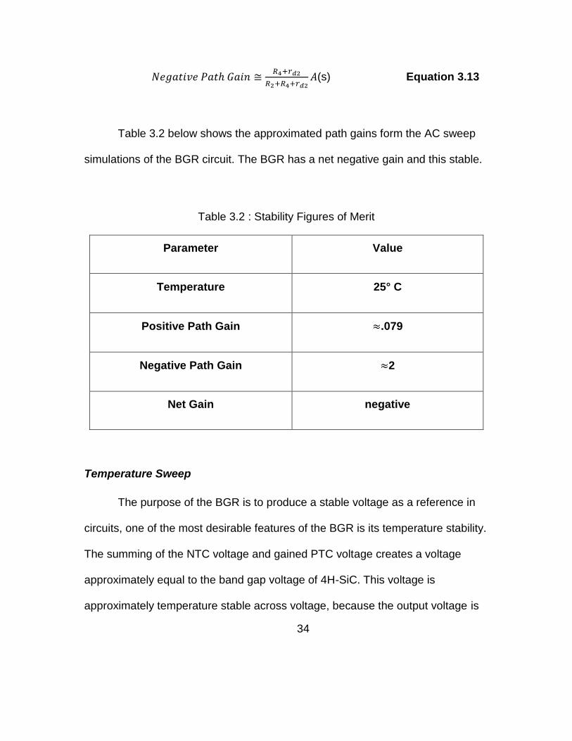
𝑅2+𝑅4+𝑟𝑑2𝐴(s) Equation 3.13
Table 3.2 below shows the approximated path gains form the AC sweep
simulations of the BGR circuit. The BGR has a net negative gain and this stable.
Table 3.2 : Stability Figures of Merit
Parameter Value
Temperature 25° C
Positive Path Gain ≈.079
Negative Path Gain ≈2
Net Gain negative
Temperature Sweep
The purpose of the BGR is to produce a stable voltage as a reference in
circuits, one of the most desirable features of the BGR is its temperature stability.
The summing of the NTC voltage and gained PTC voltage creates a voltage
approximately equal to the band gap voltage of 4H-SiC. This voltage is
approximately temperature stable across voltage, because the output voltage is
35
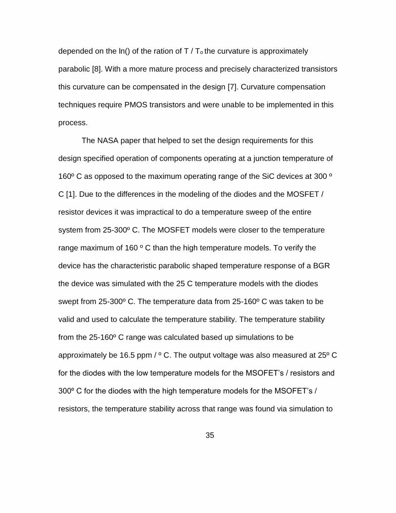
depended on the ln() of the ration of T / To the curvature is approximately
parabolic [8]. With a more mature process and precisely characterized transistors
this curvature can be compensated in the design [7]. Curvature compensation
techniques require PMOS transistors and were unable to be implemented in this
process.
The NASA paper that helped to set the design requirements for this
design specified operation of components operating at a junction temperature of
160º C as opposed to the maximum operating range of the SiC devices at 300 º
C [1]. Due to the differences in the modeling of the diodes and the MOSFET /
resistor devices it was impractical to do a temperature sweep of the entire
system from 25-300º C. The MOSFET models were closer to the temperature
range maximum of 160 º C than the high temperature models. To verify the
device has the characteristic parabolic shaped temperature response of a BGR
the device was simulated with the 25 C temperature models with the diodes
swept from 25-300º C. The temperature data from 25-160º C was taken to be
valid and used to calculate the temperature stability. The temperature stability
from the 25-160º C range was calculated based up simulations to be
approximately be 16.5 ppm / º C. The output voltage was also measured at 25º C
for the diodes with the low temperature models for the MSOFET’s / resistors and
300º C for the diodes with the high temperature models for the MSOFET’s /
resistors, the temperature stability across that range was found via simulation to
36
approximately be 34.5 ppm / º C. The 25-160º C simulation is below. This
simulation includes data beyond the 160º C temperature.
Kuijk BGR Schematic and Layout
The uncertainties created by issues with device modeling were mitigated
by giving maximum visibility into the BGR design. The diode resistor network,
start up circuit, and operational amplifier were pinned out separately. This allows
the connections between the BGR blocks to be done off chip where they can be
easily modified and allow for the use of external components, see figure 3.9.
Figure 3.10 shows the final BGR IC layout. Block 2 is the startup network, block 3
is the diode resistor network, and block 4 is the operational amplifier. The IC
shares space with the oscillator driver circuit.

37
Figure 3.8 : BGR Temperature Sweep Output

38
Figure 3.9 : BGR IC Block Diagram

39
Figure : 3.10 SiC BGR Layout

40
Chapter Four :
SiC BGR Reference Test
The SiC process that is used for this design is not a major production
process, at the time of writing the SiC BGR chip is still in production. This chapter
will cover the philosophy of testing, the test plan for the BGR, and the BGR test
schematic.
With the risks associated with the immature SiC process and inconsistent
models, the design philosophy was to provide maximum flexibility in
implementing the BGR on a printed circuit card and give maximum visibility to the
BGR subcomponents. Thus allowing characterization of the diode and diode
pairs individually, and to allow substitution of on chip components with off chip
commercial components. This gives a path to success in the global goal of a
BGR that can operate at the 160º C range even if commercial high temperature
Silicon operational amplifiers and high temperature off chip passive components
are needed.
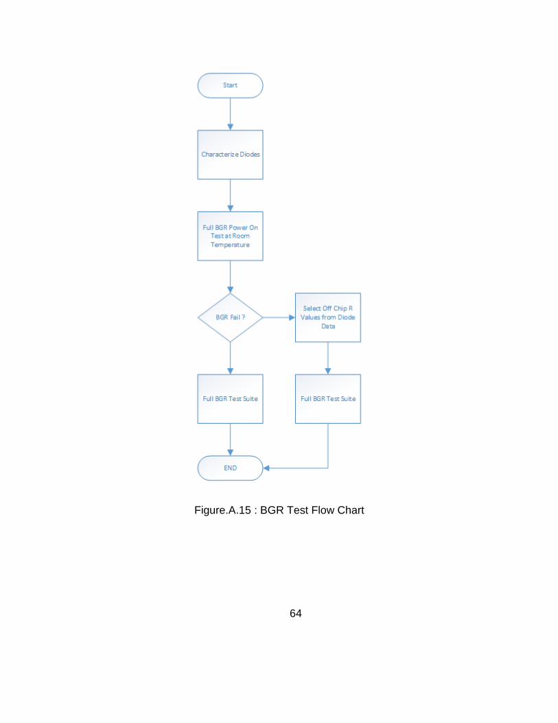
BGR Test Plan
The BGR plan consists of generating I-V curves for the diode and diode
pairs at 25 º C, 100 º C, 150 º C, and 200 º C, performing a basic power up test

41
of the full on chip BGR, then proceeding with the full BGR test suite on the full on
chip BGR or selecting resistor values and testing the BGR with the off chip
auxiliary amplifier. A flow chart for the BGR test plan is in the appendix.
The IV curves will be generated across the 0-5V forward voltage range
using a high precision meter. The temperature will be swept using the ICASL
oven. This data will then be plotted and compared to the design simulation data
performed earlier.
The basic power up test consists of using a lab power supply to power the
assembled test card configured for on chip operation. The power supply voltage
for the chip will be 24V DC. The output of the BGR will be monitored with a high
precision meter and oscilloscope. The oscilloscope will be used to observe any
oscillation or ringing on the BGR output. The operating current will also be
monitored.
If the BGR in the on chip configuration powers up and reaches the band
gap design voltage at room temperature, the configuration will be tested with the
full BGR test. If the BGR does not function the IV curve data from the initial diode
test will be used to select components for the external resistor network and the
external auxiliary amp will be used. The BGR test suit is in the following
paragraphs. The load for all of the previous tests will be a 1Meg resistor and
20pF capacitor.
42
The full BGR test suit consists of a startup transient tests of the BGR with
500ns, 1µs, and 2µs rise times. The rail voltage will be raised from 0-24V at 25º
C and 160º C in the ICASL oven. The output voltage will be monitored for DC
level and AC anomalies. The 25º C will be compared to the simulation data. This
data will show that the BGR circuit is stable. The test will be repeated with 22V
and 26V supply voltages.
The BGR circuit will then be heated from 25-160º C with continuous 24V
supply voltage. The output voltage will be logged as well as monitored for AC
anomalies. This will verify the temperature stability of the design across its
operating range [7]. The test will be repeated with 22V and 26V supply voltages.
The BGR circuit will then be heated to 25º C with continuous 24V supply
voltage and then to 160º C. The output voltage will be logged as well as
monitored for AC anomalies. The test will be repeated with 22V and 26V supply
voltages. This test will characterize the line regulation of the design [7].
The BGR circuit will then be heated from 25-160º C with continuous 24V
supply voltage and then cooled from 160-25º C The output voltage will be logged
as well as monitored for AC anomalies. The test will be repeated with 22V and
26V supply voltages. This test will measure the temperature hysteresis of the
BGR design. [10]
The BGR circuit will then be heated to 25º C with continuous 24V supply
voltage and then to 160º C . The output voltage will be logged as well as
43
monitored for AC anomalies, the supply current will also be measured. The test
will be repeated with 22V and 26V supply voltages. The load for this test will be a
20pF capacitor. This test will measure the quiescent current of the BGR design
and the open circuit voltage [7].
In the event the auxiliary amplifier and external resistors must be used the
maximum test temperature will be lowered to be within the operating range of the
external components.
BGR Test Schematic
The BGR test circuit consists of the SiC BGR IC, an external resistor
network, and an auxiliary amplifier. The auxiliary amplifier selected is a Texas
Instruments OPA211AIDR. It is a silicon rail to rail amplifier that supports the 24V
rail It also comes in a standard operating temperature part which will be used for
testing and an HT version that has an operating range of up to 210 C [16].
The BGR IC is connected to the auxiliary amplifier, external resistors, and
feedback paths via surface mount jumpers. These are zero ohm resistors that
can be placed to select the configuration of the board. The startup circuit is also
connected via resistor placements. These can be filled with zero ohm jumpers or
resistive dividers depending on the required start up voltages. This allows the
test card to use the startup diode network even if there is an error in the forward
voltage of the diodes. The resistive divider allows find tuning of the voltage
supplied to start the BGR IC. The BGR test schematic is below

44
Figure 4.1 : SiC BGR Test Circuit

45
Chapter Five :
Conclusions
In this paper the design of a single chip Kuijk BGR in SiC along with the
test circuit and test plan were covered. The goal of temperature stability across
the 25-160º C operating temperature range was shown in simulation. The IC was
laid out and successfully met the design rules of the fabrication process owner. A
circuit and test plan were created to verify the operation of the IC once it
completes fabrication. The uncertainty created by device modeling issues and
inability to conduct post layout simulation was mitigated by having high visibility
into the IC.
Production delays have prevented the testing of the fabricated circuit.
Future work should consist of testing the fabricated IC to the test plan. This
would include creating IV curves for the diode and generating temperature sweep
data of the IV curve. Future runs could use the accurate diode data to more
accurately select values for the BGR resistor network. Further work should also
be done to characterize the NMOS transistor, with continuous temperature
models.

46
LIST OF REFERENCES
47
[1] G. A. Carr, C. J. Iannello, Y. Chen, D. J. Hunter, L. Del
Castillo, A. T. Bradley, C. Stell and M. Mojarradi, "Extreem
Environment Capable, Modular and Scalable Power Processing Unit
for Solar Electric Propulsion," in Aerospace Conference, Big Sky,
2013.
[2] V. Banu, P. Brosselard, X. Jorda, P. Godingnon and J. Millan,
"Demonstration of High Temperature Bandgap Voltage Reference
Feasibility on SiC Material," Material Science Forum, pp. 1131-1134,
2010.
[3] V. Banu, P. Godignon, X. Jorda, M. Alexandru and J. Millan,
"Study on the Fesaibility of SiC Bandgap Voltage Reference for High
Temperature Applications," Material Science Forum, pp. 754-757,
2011.
[4] C.-W. Kok and W.-S. Tam, CMOS Voltage References: An
analytical and practical perspective, Singapore: Wiley, 2013.
[5] P. R. Gray, P. J. Hurst, S. H. Lewis and R. G. Myer, Analysis
and Design of Analog Integrated Circuits, Honoken: Wiley, 2009.
[6] M. Lee, "Application Note 82: Understanding and Applying
Voltage References," Linear Technology, Milpitas, 1999.

48
[7] K. E. Kuijk, "A Precision Reference Voltage Source," IEEE
Journal of Solid-State Circuits, pp. 222-226, 1973.
[8] R. Blauschild, P. A. Tucci, R. S. Muller and R. G. Meyer, "A
new NMOS temperature-stable voltage reference," IEEE Journal of
Solid State Circuits, vol. 13, no. 6, pp. 767 - 774, 1978.
[9] M. B. R. B. R. C. B. J. C. D. S. K. M. G. C. C. R. G. Harris
R.K, A Silicon Carbide Integrated Circuit Implementing, Long Beach:
APEC, 2016.
[10] A. P. Brokaw, "A Simple Three Terminal IC Bandgap
Rrefernece," IEEE Journal of Solid State Circuits, vol. 9, no. 6, pp.
388-393, 1974.
[11] R. A. Pease, "The Design of Band-Gap Reference Circuits:
Trials and Tribulations," in IEEE Bipoalr Cricuits and Technology
Meeting, Minneapolis, 1990.
[12] M. Hasanuzzamana, S. K. Islam, L. M. Tolbert and M. T.
Alam, "Temperature dependency of MOSFET device characteristics
in 4H- and 6H-silicon carbide (SiC)," Solid-State Electronics, vol. 48,
no. 10-11, p. 1877–1881, 2004.
[13] D. A. Neamen, Semiconductor Physics And Devices: Basic
Principles, New York: McGraw-Hill, 2011.

49
[14] J. Casady and J. R.W, "STATUS OF SILICON CARBIDE AS
A WIDE BANDGAP SEMICONDUCTOR FOR HIGH
TEMPERATURE APPLICATIONS: A REVIEW," Solid State
Electronics, vol. 39, no. 10, pp. 1409-1422, 1996.
[15] A. Vert, C.-P. Chen, A. Patil, R. Saia, E. Anadarawis, A.
Kashyap, T. Zhang and D. Shaddock, "Silicon Carbide High
Temperature Operational Amplifier," in IMAPS High Temperaure
Electronics Conference (HiTEC), Albuquerque, 2012.
[16] K. Blake, "Op Amp Precision Design : DC Errors," Microchip
Technology, Chandler, 2008.
[17] R. Palmer, "DC Paramaters : Input Offset Voltage," Texas
Instruments, Houston, 2001.
[18] J. Wright, "Linear Technology Design Notes: Don't be Fooled
by Voltage Reference Long-Term Drift and Hysterisis," Linear
Technology, Milpitas, 2000.
[19] Texas Instruments, OPA211 : 1.1nV/rtHz Noise, Low Power,
Precision Operational Amplifier, Houston: Texas Instruments, 2015.

50
APPENDIX
51
Figure.A.1 : Resistor Layout
Figure.A.2 : Diode Layout
52
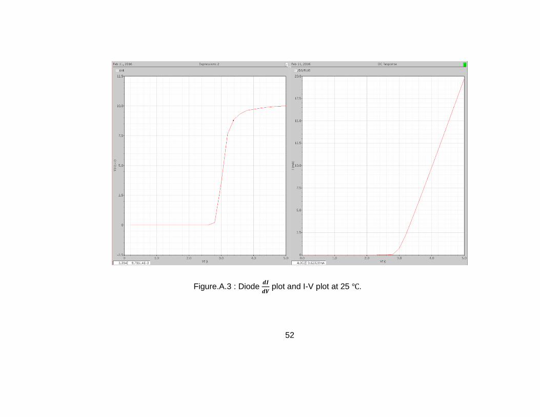
Figure.A.3 : Diode 𝒅𝑰
𝒅𝑽 plot and I-V plot at 25 .

53
Figure.A.4 : I-V plot Temperature Sweep, 25 - 300 .

54
Figure.A.5 : Op Amp Open Loop Response at 𝟐𝟓 .

55
Figure.A.6 : Op Amp Open Loop Response at 𝟑𝟎𝟎 .
56
Figure.A.7 : BGR Start Up Circuit
57
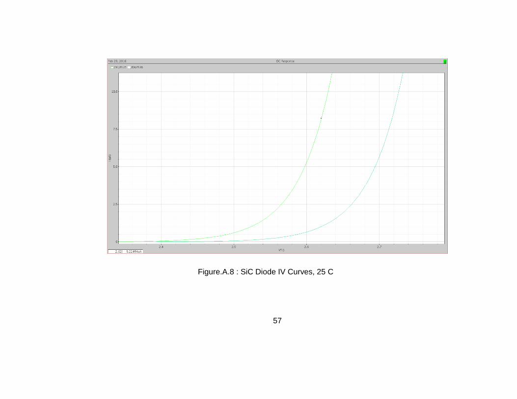
Figure.A.8 : SiC Diode IV Curves, 25 C

58
Figure.A.9 : Schematic of Diode NTC - PTC Temperature Sweep

59
Figure.A.10 : Diode NTC - PTC Temperature Sweep
60
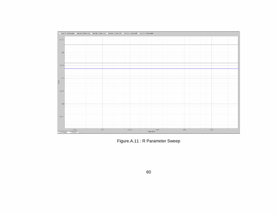
Figure.A.11 : R Parameter Sweep
61
Figure.A.12 : 500ns Rise Time Start Up Simulation, Vout
62
Figure.A.13 : 1us Rise Time Start Up Simulation, Vout

63
Figure.A.14 : 5us Rise Time Start Up Simulation, Vout
64
Figure.A.15 : BGR Test Flow Chart
65
VITA
Charles K Roberts was born in Hopewell, VA to parents Charles
and Helen Roberts. He attended Hopewell High School in Hopewell, VA. He
enrolled at the University of Tennessee at Knoxville where he received his
Bachelor of Science in Electrical Engineering in May 2015. During his
undergraduate and graduate career at UT-Knoxville Charles worked at Oak
Ridge National Laboratory as a Data Acquisition Engineer. He was awarded the
Bodenheimer Fellowship and continued his studies with the Integrated Circuits
and Systems Laboratory under Professor Benjamin Blalock. Charles lives in Oak
Ridge, TN with his wife Laura and sons Liam and Ethan. He anticipates earning
his −Master of Science in Electrical Engineering from UT in the spring of 2016.