Si86xx 1 Mbps Data Sheet
47
Si86xx 1 Mbps Data Sheet 1 Mbps, 2.5 kV RMS Digital Isolators Skyworks' family of ultra-low-power digital isolators are CMOS devices offering substan- tial data rate, propagation delay, power, size, reliability, and external BOM advantages over legacy isolation technologies. The operating parameters of these products remain stable across wide temperature ranges and throughout device service life for ease of design and highly uniform performance. All device versions have Schmitt trigger inputs for high noise immunity and only require VDD bypass capacitors. All products support Data rates up to 1 Mbps and Enable inputs which provide a single point control for enabling and disabling output drive. All products are safety certified by UL, CSA, VDE, and CQC and support withstand ratings up to 2.5 kV RMS . Automotive Grade is available for certain part numbers. These products are built using automotive-specific flows at all steps in the manufacturing process to ensure the robust- ness and low defectivity required for automotive applications. KEY FEATURES • High-speed operation • DC to 1 Mbps • No start-up initialization required • Wide Operating Supply Voltage • 2.5 to 5.5 V • Up to 2500 V RMS isolation • 60-year life at rated working voltage • High electromagnetic immunity • Ultra low power (typical) • 5 V Operation: 1.6 mA per channel at 1 Mbps • 2.5 V Operation: 1.5 mA per channel at 1 Mbps • Tri-state outputs with ENABLE • Schmitt trigger inputs • Transient Immunity 50 kV/µs • AEC-Q100 qualification • Wide temperature range • –40 to 125 °C • RoHS-compliant packages • SOIC-16 wide body • SOIC-16 narrow body • SOIC-8 narrow body • Automotive-grade OPNs available • AIAG compliant PPAP documentation support • IMDS and CAMDS listing support Industrial Applications • Industrial automation systems • Medical electronics • Isolated switch mode supplies • Isolated ADC, DAC • Motor control • Power inverters • Communication systems Safety Regulatory Approvals • UL 1577 recognized • Up to 5000 V RMS for 1 minute • CSA component notice 5A approval • IEC 60950-1, 61010-1 • VDE certification conformity • IEC 60747-5-2 (VDE0884 Part 2) • CQC certification approval • GB4943.1 Automotive Applications • On-board chargers • Battery management systems • Charging stations • Traction inverters • Hybrid Electric Vehicles • Battery Electric Vehicles Skyworks Solutions, Inc. • Phone [781] 376-3000 • Fax [781] 376-3100 • [email protected] • www.skyworksinc.com 1 Rev. 1.03 • Skyworks Proprietary Information • Products and Product Information are Subject to Change Without Notice • November 10, 2021 1
Transcript of Si86xx 1 Mbps Data Sheet

Si86xx 1 Mbps Data Sheet
1 Mbps, 2.5 kVRMS Digital Isolators
Skyworks' family of ultra-low-power digital isolators are CMOS devices offering substan-tial data rate, propagation delay, power, size, reliability, and external BOM advantagesover legacy isolation technologies. The operating parameters of these products remainstable across wide temperature ranges and throughout device service life for ease ofdesign and highly uniform performance. All device versions have Schmitt trigger inputsfor high noise immunity and only require VDD bypass capacitors.
All products support Data rates up to 1 Mbps and Enable inputs which provide a singlepoint control for enabling and disabling output drive. All products are safety certified byUL, CSA, VDE, and CQC and support withstand ratings up to 2.5 kVRMS.
Automotive Grade is available for certain part numbers. These products are built usingautomotive-specific flows at all steps in the manufacturing process to ensure the robust-ness and low defectivity required for automotive applications.
KEY FEATURES
• High-speed operation• DC to 1 Mbps
• No start-up initialization required• Wide Operating Supply Voltage
• 2.5 to 5.5 V• Up to 2500 VRMS isolation
• 60-year life at rated working voltage• High electromagnetic immunity• Ultra low power (typical)
• 5 V Operation: 1.6 mA per channel at 1Mbps
• 2.5 V Operation: 1.5 mA per channel at1 Mbps
• Tri-state outputs with ENABLE• Schmitt trigger inputs• Transient Immunity 50 kV/µs• AEC-Q100 qualification• Wide temperature range
• –40 to 125 °C• RoHS-compliant packages
• SOIC-16 wide body• SOIC-16 narrow body• SOIC-8 narrow body
• Automotive-grade OPNs available• AIAG compliant PPAP documentation
support• IMDS and CAMDS listing support
Industrial Applications• Industrial automation systems• Medical electronics• Isolated switch mode supplies• Isolated ADC, DAC• Motor control• Power inverters• Communication systems
Safety Regulatory Approvals• UL 1577 recognized
• Up to 5000 VRMS for 1 minute• CSA component notice 5A approval
• IEC 60950-1, 61010-1• VDE certification conformity
• IEC 60747-5-2 (VDE0884 Part 2)• CQC certification approval
• GB4943.1
Automotive Applications• On-board chargers• Battery management systems• Charging stations• Traction inverters• Hybrid Electric Vehicles• Battery Electric Vehicles
Skyworks Solutions, Inc. • Phone [781] 376-3000 • Fax [781] 376-3100 • [email protected] • www.skyworksinc.com1 Rev. 1.03 • Skyworks Proprietary Information • Products and Product Information are Subject to Change Without Notice • November 10, 2021 1

1. Ordering Guide
Industrial and Automotive Grade OPNs
Industrial-grade devices (part numbers having an “-I” in their suffix) are built using well-controlled, high-quality manufacturing flows toensure robustness and reliability. Qualifications are compliant with JEDEC, and defect reduction methodologies are used throughoutdefinition, design, evaluation, qualification, and mass production steps.
Automotive-grade devices (part numbers having an “-A” in their suffix) are built using automotive-specific flows at all steps in themanufacturing process to ensure robustness and low defectivity. These devices are supported with AIAG-compliant Production PartApproval Process (PPAP) documentation, and feature International Material Data System (IMDS) and China Automotive MaterialData System (CAMDS) listing. Qualifications are compliant with AEC-Q100, and a zero-defect methodology is maintained throughoutdefinition, design, evaluation, qualification, and mass production steps.
Table 1.1. Ordering Guide for Valid OPNs1, 2, 4
Ordering Part Number(OPN)
Automotive OPNs5, 6 Numberof In-puts
VDD1Side
Numberof In-puts
VDD2Side
MaxDataRate
(Mbps)
DefaultOutputState
Isola-tion
Rating(kV)
Package
Si8610AB-B-IS Si8610AB-AS 1 0 1 Low 2.5 SOIC-8
Si8620AB-B-IS Si8620AB-AS 2 0 1 Low 2.5 SOIC-8
Si8621AB-B-IS Si8621AB-AS 1 1 1 Low 2.5 SOIC-8
Si8630AB-B-IS Si8630AB-AS 3 0 1 Low 2.5 WB SOIC-16
Si8630AB-B-IS1 Si8630AB-AS1 3 0 1 Low 2.5 NB SOIC-16
Si8631AB-B-IS Si8631AB-AS 2 1 1 Low 2.5 WB SOIC-16
Si8631AB-B-IS1 Si8631AB-AS1 2 1 1 Low 2.5 NB SOIC-16
Si8640AB-B-IS1 Si8640AB-AS1 4 0 1 Low 2.5 NB SOIC-16
Si8640AB-B-IS Si8640AB-AS 4 0 1 Low 2.5 WB SOIC-16
Si8641AB-B-IS1 Si8641AB-AS1 3 1 1 Low 2.5 NB SOIC-16
Si8641AB-B-IS Si8641AB-AS 3 1 1 Low 2.5 WB SOIC-16
Si8642AB-B-IS1 Si8642AB-AS1 2 2 1 Low 2.5 NB SOIC-16
Si8642AB-B-IS Si8642AB-AS 2 2 1 Low 2.5 WB SOIC-16
Si8650AB-B-IS1 Si8650AB-AS1 5 0 1 Low 2.5 NB SOIC-16
Si8651AB-B-IS1 Si8651AB-AS1 4 1 1 Low 2.5 NB SOIC-16
Si8652AB-B-IS1 Si8652AB-AS1 3 2 1 Low 2.5 NB SOIC-16
Si8660AB-B-IS1 Si8660AB-AS1 6 0 1 Low 2.5 NB SOIC-16
Si8661AB-B-IS1 Si8661AB-AS1 5 1 1 Low 2.5 NB SOIC-16
Si8662AB-B-IS1 Si8662AB-AS1 4 2 1 Low 2.5 NB SOIC-16
Si8663AB-B-IS1 Si8663AB-AS1 3 3 1 Low 2.5 NB SOIC-16
Si86xx 1 Mbps Data Sheet • Ordering Guide
Skyworks Solutions, Inc. • Phone [781] 376-3000 • Fax [781] 376-3100 • [email protected] • www.skyworksinc.com2 Rev. 1.03 • Skyworks Proprietary Information • Products and Product Information are Subject to Change Without Notice • November 10, 2021 2

Ordering Part Number(OPN)
Automotive OPNs5, 6 Numberof In-puts
VDD1Side
Numberof In-puts
VDD2Side
MaxDataRate
(Mbps)
DefaultOutputState
Isola-tion
Rating(kV)
Package
Notes:1. All packages are RoHS-compliant with peak reflow temperatures of 260 °C according to the JEDEC industry standard classifica-
tions and peak solder temperatures.2. “Si” and “SI” are used interchangeably.3. An "R" at the end of the part number denotes tape and reel packaging option.4. Temperature range is –40 to 125 °C.5. Automotive-Grade devices (with an "–A" suffix) are identical in construction materials, topside marking, and electrical parameters
to their Industrial-Grade (with an "–I" suffix) version counterparts. Automotive-Grade products are produced utilizing full automo-tive process flows and additional statistical process controls throughout the manufacturing flow. The Automotive-Grade partnumber is included on shipping labels.
6. In the top markings of each device, the Manufacturing Code represented by either “RTTTTT” or “TTTTTT” contains as its firstcharacter a letter in the range N through Z to indicate Automotive-Grade.
Si86xx 1 Mbps Data Sheet • Ordering Guide
Skyworks Solutions, Inc. • Phone [781] 376-3000 • Fax [781] 376-3100 • [email protected] • www.skyworksinc.com3 Rev. 1.03 • Skyworks Proprietary Information • Products and Product Information are Subject to Change Without Notice • November 10, 2021 3

Table of Contents1. Ordering Guide . . . . . . . . . . . . . . . . . . . . . . . . . . . . . . 2
2. Functional Description. . . . . . . . . . . . . . . . . . . . . . . . . . . . 52.1 Theory of Operation . . . . . . . . . . . . . . . . . . . . . . . . . . . . 5
3. Device Operation . . . . . . . . . . . . . . . . . . . . . . . . . . . . . . 63.1 Device Startup . . . . . . . . . . . . . . . . . . . . . . . . . . . . . . 8
3.2 Undervoltage Lockout . . . . . . . . . . . . . . . . . . . . . . . . . . . 8
3.3 Layout Recommendations . . . . . . . . . . . . . . . . . . . . . . . . . . 83.3.1 Supply Bypass . . . . . . . . . . . . . . . . . . . . . . . . . . . . 83.3.2 Output Pin Termination . . . . . . . . . . . . . . . . . . . . . . . . . . 8
4. Electrical Specifications . . . . . . . . . . . . . . . . . . . . . . . . . . . 9
5. Pin Descriptions . . . . . . . . . . . . . . . . . . . . . . . . . . . . . 305.1 Pin Descriptions (Si861x/2x Narrow Body SOIC-8) . . . . . . . . . . . . . . . . . .30
5.2 Pin Descriptions (Si863x) . . . . . . . . . . . . . . . . . . . . . . . . . .31
5.3 Pin Descriptions (Si864x) . . . . . . . . . . . . . . . . . . . . . . . . . .32
5.4 Pin Descriptions (Si8650/51/52) . . . . . . . . . . . . . . . . . . . . . . . .33
5.5 Pin Descriptions (Si866x) . . . . . . . . . . . . . . . . . . . . . . . . . .34
6. Package Outlines . . . . . . . . . . . . . . . . . . . . . . . . . . . . . 356.1 Package Outline (16-Pin Wide Body SOIC) . . . . . . . . . . . . . . . . . . . .35
6.2 Package Outline (16-Pin Narrow Body SOIC). . . . . . . . . . . . . . . . . . . .37
6.3 Package Outline (8-Pin Narrow Body SOIC) . . . . . . . . . . . . . . . . . . . .39
7. Land Patterns . . . . . . . . . . . . . . . . . . . . . . . . . . . . . . 407.1 Land Pattern (16-Pin Wide-Body SOIC) . . . . . . . . . . . . . . . . . . . . .40
7.2 Land Pattern (16-Pin Narrow Body SOIC) . . . . . . . . . . . . . . . . . . . . .41
7.3 Land Pattern (8-Pin Narrow Body SOIC) . . . . . . . . . . . . . . . . . . . . .42
8. Top Markings . . . . . . . . . . . . . . . . . . . . . . . . . . . . . . 438.1 Top Marking (16-Pin Wide Body SOIC) . . . . . . . . . . . . . . . . . . . . . .43
8.2 Top Marking (16-Pin Narrow Body SOIC) . . . . . . . . . . . . . . . . . . . . .44
8.3 Top Marking (8-Pin Narrow Body SOIC) . . . . . . . . . . . . . . . . . . . . .45
9. Revision History . . . . . . . . . . . . . . . . . . . . . . . . . . . . . 46
Skyworks Solutions, Inc. • Phone [781] 376-3000 • Fax [781] 376-3100 • [email protected] • www.skyworksinc.com4 Rev. 1.03 • Skyworks Proprietary Information • Products and Product Information are Subject to Change Without Notice • November 10, 2021 4

2. Functional Description
2.1 Theory of Operation
The operation of an Si86xx channel is analogous to that of an opto coupler, except an RF carrier is modulated instead of light. Thissimple architecture provides a robust isolated data path and requires no special considerations or initialization at start-up. A simplifiedblock diagram for a single Si86xx channel is shown in the figure below.
RF OSCILLATOR
MODULATOR DEMODULATORA BSemiconductor-Based Isolation
Barrier
Transmitter Receiver
Figure 2.1. Simplified Channel Diagram
A channel consists of an RF Transmitter and RF Receiver separated by a semiconductor-based isolation barrier. Referring to theTransmitter, input A modulates the carrier provided by an RF oscillator using on/off keying. The Receiver contains a demodulator thatdecodes the input state according to its RF energy content and applies the result to output B via the output driver. This RF on/off keyingscheme is superior to pulse code schemes as it provides best-in-class noise immunity, low power consumption, and better immunity tomagnetic fields. See the figure below for more details.
Input Signal
Output Signal
Modulation Signal
Figure 2.2. Modulation Scheme
Si86xx 1 Mbps Data Sheet • Functional Description
Skyworks Solutions, Inc. • Phone [781] 376-3000 • Fax [781] 376-3100 • [email protected] • www.skyworksinc.com5 Rev. 1.03 • Skyworks Proprietary Information • Products and Product Information are Subject to Change Without Notice • November 10, 2021 5

3. Device Operation
Device behavior during start-up, normal operation, and shutdown is shown in Figure 3.1 Device Behavior during Normal Operation onpage 8, where UVLO+ and UVLO- are the positive-going and negative-going thresholds respectively. Refer to the table below todetermine outputs when power supply (VDD) is not present. Additionally, refer to Table 3.2 Enable Input Truth1 on page 7 for logicconditions when enable pins are used.
Table 3.1. Si86xx Logic Operation
VIInput1,2
ENInput1,2,3,4
VDDIState1,5,6
VDDOState1,5,6
VO Output1,2 Comments
H H or NC P P H Enabled, normal operation.
L H or NC P P L
X7 L P P Hi-Z8 Disabled.
X7 H or NC UP P L Upon transition of VDDI from unpowered to powered, VOreturns to the same state as VI in less than 1 µs.
X7 L UP P Hi-Z8 Disabled.
X7 X7 P UP Undetermined Upon transition of VDDO from unpowered to powered, VOreturns to the same state as VI within 1 µs, if EN is in eitherthe H or NC state. Upon transition of VDDO from unpoweredto powered, VO returns to Hi-Z within 1 µs if EN is L.
Notes:1. VDDI and VDDO are the input and output power supplies. VI and VO are the respective input and output terminals. EN is the
enable control input located on the same output side.2. X = not applicable; H = Logic High; L = Logic Low; Hi-Z = High Impedance.3. It is recommended that the enable inputs be connected to an external logic high or low level when the Si86xx is operating in noisy
environments.4. No Connect (NC) replaces EN1 on some devices. No Connects are not internally connected and can be left floating, tied to VDD,
or tied to GND.5. “Powered” state (P) is defined as 2.5 V < VDD < 5.5 V.6. “Unpowered” state (UP) is defined as VDD = 0 V.7. Note that an I/O can power the die for a given side through an internal diode if its source has adequate current.8. When using the enable pin (EN) function, the output pin state is driven into a high-impedance state when the EN pin is disabled
(EN = 0).
Si86xx 1 Mbps Data Sheet • Device Operation
Skyworks Solutions, Inc. • Phone [781] 376-3000 • Fax [781] 376-3100 • [email protected] • www.skyworksinc.com6 Rev. 1.03 • Skyworks Proprietary Information • Products and Product Information are Subject to Change Without Notice • November 10, 2021 6

Table 3.2. Enable Input Truth1
P/N EN11,2 EN21,2 Operation
Si861x/2x — — Outputs are enabled and follow input state.
Si8630 — H Outputs B1, B2, B3 are enabled and follow input state.
— L Outputs B1, B2, B3 are disabled and in high impedance state.3
Si8631 H X Output A3 enabled and follows input state.
L X Output A3 disabled and in high impedance state.3
X H Outputs B1, B2 are enabled and follow input state.
X L Outputs B1, B2 are disabled and in high impedance state.3
Si8640 — H Outputs B1, B2, B3, B4 are enabled and follow the input state.
— L Outputs B1, B2, B3, B4 are disabled and in high impedance state.3
Si8641 H X Output A4 enabled and follows the input state.
L X Output A4 disabled and in high impedance state.3
X H Outputs B1, B2, B3 are enabled and follow the input state.
X L Outputs B1, B2, B3 are disabled and in high impedance state.3
Si8642 H X Outputs A3 and A4 are enabled and follow the input state.
L X Outputs A3 and A4 are disabled and in high impedance state.3
X H Outputs B1 and B2 are enabled and follow the input state.
X L Outputs B1 and B2 are disabled and in high impedance state.3
Si8650 — H Outputs B1, B2, B3, B4, B5 are enabled and follow input state.
— L Outputs B1, B2, B3, B4, B5 are disabled and Logic Low or in high impedance state.3
Si8651 H X Output A5 enabled and follow input state.
L X Output A5 disabled and in high impedance state.3
X H Outputs B1, B2, B3, B4 are enabled and follow input state.
X L Outputs B1, B2, B3, B4 are disabled and in high impedance state.3
Si8652 H X Outputs A4 and A5 are enabled and follow input state.
L X Outputs A4 and A5 are disabled and in high impedance state.3
X H Outputs B1, B2, B3 are enabled and follow input state.
X L Outputs B1, B2, B3 are disabled and in high impedance state.3
Si866x — — Outputs are enabled and follow input state.
Notes:1. Enable inputs EN1 and EN2 can be used for multiplexing, for clock sync, or other output control. These inputs are internally
pulled-up to local VDD by a 2 µA current source allowing them to be connected to an external logic level (high or low) or leftfloating. To minimize noise coupling, do not connect circuit traces to EN1 or EN2 if they are left floating. If EN1, EN2 are unused,it is recommended they be connected to an external logic level, especially if the Si86xx is operating in a noisy environment.
2. X = not applicable; H = Logic High; L = Logic Low.3. When using the enable pin (EN) function, the output pin state is driven into a high-impedance state when the EN pin is disabled
(EN = 0).
Si86xx 1 Mbps Data Sheet • Device Operation
Skyworks Solutions, Inc. • Phone [781] 376-3000 • Fax [781] 376-3100 • [email protected] • www.skyworksinc.com7 Rev. 1.03 • Skyworks Proprietary Information • Products and Product Information are Subject to Change Without Notice • November 10, 2021 7

3.1 Device Startup
Outputs are held low during powerup until VDD is above the UVLO threshold for time period tSTART. Following this, the outputs followthe states of inputs.
3.2 Undervoltage Lockout
Undervoltage Lockout (UVLO) is provided to prevent erroneous operation during device startup and shutdown or when VDD is below itsspecified operating circuits range. Both Side A and Side B each have their own undervoltage lockout monitors. Each side can enter orexit UVLO independently. For example, Side A unconditionally enters UVLO when VDD1 falls below VDD1(UVLO–) and exits UVLO whenVDD1 rises above VDD1(UVLO+). Side B operates the same as Side A with respect to its VDD2 supply.
INPUT
VDD1
UVLO-
VDD2
UVLO+
UVLO-UVLO+
OUTPUT
tSTART tSTART tSTARTtPHL tPLHtSD
Figure 3.1. Device Behavior during Normal Operation
3.3 Layout Recommendations
To ensure safety in the end user application, high voltage circuits (i.e., circuits with >30 VAC) must be physically separated from thesafety extra-low voltage circuits (SELV is a circuit with <30 VAC) by a certain distance (creepage/clearance). If a component, such as adigital isolator, straddles this isolation barrier, it must meet those creepage/clearance requirements and also provide a sufficiently largehigh-voltage breakdown protection rating (commonly referred to as working voltage protection). Table 4.5 Regulatory Information1 onpage 25 and Table 4.6 Insulation and Safety-Related Specifications on page 25 detail the working voltage and creepage/clearancecapabilities of the Si86xx. These tables also detail the component standards (UL1577, IEC60747, CSA 5A), which are readily acceptedby certification bodies to provide proof for end-system specifications requirements. Refer to the end-system specification (61010-1,60950-1, 60601-1, etc.) requirements before starting any design that uses a digital isolator.
3.3.1 Supply Bypass
The Si86xx family requires a 0.1 µF bypass capacitor between VDD1 and GND1 and VDD2 and GND2. The capacitor should be placedas close as possible to the package. To enhance the robustness of a design, the user may also include resistors (50–300 Ω ) in serieswith the inputs and outputs if the system is excessively noisy.
3.3.2 Output Pin Termination
The nominal output impedance of an isolator driver channel is approximately 50 Ω, ±40%, which is a combination of the value of theon-chip series termination resistor and channel resistance of the output driver FET. When driving loads where transmission line effectswill be a factor, output pins should be appropriately terminated with controlled impedance PCB traces.
Si86xx 1 Mbps Data Sheet • Device Operation
Skyworks Solutions, Inc. • Phone [781] 376-3000 • Fax [781] 376-3100 • [email protected] • www.skyworksinc.com8 Rev. 1.03 • Skyworks Proprietary Information • Products and Product Information are Subject to Change Without Notice • November 10, 2021 8

4. Electrical Specifications
Table 4.1. Recommended Operating Conditions
Parameter Symbol Min Typ Max Unit
Ambient Operating Temperature1 TA –40 25 125 ºC
Supply VoltageVDD1 2.5 — 5.5 V
VDD2 2.5 — 5.5 V
Note:1. The maximum ambient temperature is dependent on data frequency, output loading, number of operating channels, and supply
voltage.
Table 4.2. Electrical Characteristics
(VDD1 = 5 V±10%, VDD2 = 5 V±10%, TA = –40 to 125 °C)
Parameter Symbol Test Condition Min Typ Max Unit
VDD Undervoltage Threshold VDDUV+ VDD1, VDD2 rising 1.95 2.24 2.375 V
VDD Undervoltage Threshold VDDUV– VDD1, VDD2 falling 1.88 2.16 2.325 V
VDD UndervoltageHysteresis
VDDHYS 50 70 95 mV
Positive-Going Input Threshold VT+ All inputs rising 1.4 1.67 1.9 V
Negative-GoingInput Threshold
VT– All inputs falling 1.0 1.23 1.4 V
Input Hysteresis VHYS 0.38 0.44 0.50 V
High Level Input Voltage VIH 2.0 — — V
Low Level input voltage VIL — — 0.8 V
High Level Output Voltage VOH loh = –4 mA VDD1,VDD2 –0.4
4.8 — V
Low Level Output Voltage VOL lol = 4 mA — 0.2 0.4 V
Input Leakage Current IL — — ±10 µA
Output Impedance1 ZO — 50 — Ω
Enable Input High Current ΙENH VENx = VIH — 2.0 — µA
Enable Input Low Current IENL VENx = VIL — 2.0 — µA
DC Supply Current (All inputs 0 V or at Supply)
Si8610Ax
VDD1
VDD2
VDD1
VDD2
VI = 0(Ax)
VI = 0(Ax)
VI = 1(Ax)
VI = 1(Ax)
—
—
—
—
0.6
0.8
1.8
0.8
1.2
1.5
2.9
1.5
mA
Si86xx 1 Mbps Data Sheet • Electrical Specifications
Skyworks Solutions, Inc. • Phone [781] 376-3000 • Fax [781] 376-3100 • [email protected] • www.skyworksinc.com9 Rev. 1.03 • Skyworks Proprietary Information • Products and Product Information are Subject to Change Without Notice • November 10, 2021 9

Parameter Symbol Test Condition Min Typ Max Unit
Si8620Ax
VDD1
VDD2
VDD1
VDD2
VI = 0(Ax)
VI = 0(Ax)
VI = 1(Ax)
VI = 1(Ax)
—
—
—
—
0.8
1.4
3.3
1.4
1.4
2.2
5.3
2.2
mA
Si8621Ax
VDD1
VDD2
VDD1
VDD2
VI = 0(Ax)
VI = 0(Ax)
VI = 1(Ax)
VI = 1(Ax)
—
—
—
—
1.2
1.2
2.4
2.4
1.9
1.9
3.8
3.8
mA
Si8630Ax
VDD1
VDD2
VDD1
VDD2
VI = 0(Ax)
VI = 0(Ax)
VI = 1(Ax)
VI = 1(Ax)
—
—
—
—
0.9
1.9
4.6
1.9
1.6
3.0
7.4
3.0
mA
Si8631Ax
VDD1
VDD2
VDD1
VDD2
VI = 0(Ax)
VI = 0(Ax)
VI = 1(Ax)
VI = 1(Ax)
—
—
—
—
1.3
1.7
3.9
3.0
2.1
2.7
5.9
4.5
mA
Si8640Ax
VDD1
VDD2
VDD1
VDD2
VI = 0(Ax)
VI = 0(Ax)
VI = 1(Ax)
VI = 1(Ax)
—
—
—
—
1.0
2.4
6.1
2.5
1.6
3.8
9.2
4.0
mA
Si8641Ax
VDD1
VDD2
VDD1
VDD2
VI = 0(Ax)
VI = 0(Ax)
VI = 1(Ax)
VI = 1(Ax)
—
—
—
—
1.4
2.3
5.2
3.6
2.2
3.7
7.8
5.4
mA
Si8642Ax
VDD1
VDD2
VDD1
VDD2
VI = 0(Ax)
VI = 0(Ax)
VI = 1(Ax)
VI = 1(Ax)
—
—
—
—
1.8
1.8
4.4
4.4
2.9
2.9
6.6
6.6
mA
Si86xx 1 Mbps Data Sheet • Electrical Specifications
Skyworks Solutions, Inc. • Phone [781] 376-3000 • Fax [781] 376-3100 • [email protected] • www.skyworksinc.com10 Rev. 1.03 • Skyworks Proprietary Information • Products and Product Information are Subject to Change Without Notice • November 10, 2021 10

Parameter Symbol Test Condition Min Typ Max Unit
Si8650Ax
VDD1
VDD2
VDD1
VDD2
VI = 0(Ax)
VI = 0(Ax)
VI = 1(Ax)
VI = 1(Ax)
—
—
—
—
1.1
3.1
7.0
3.3
1.8
4.7
9.8
5.0
mA
Si8651Ax
VDD1
VDD2
VDD1
VDD2
VI = 0(Ax)
VI = 0(Ax)
VI = 1(Ax)
VI = 1(Ax)
—
—
—
—
1.5
2.7
6.6
4.0
2.4
4.1
9.2
6.0
mA
Si8652Ax
VDD1
VDD2
VDD1
VDD2
VI = 0(Ax)
VI = 0(Ax)
VI = 1(Ax)
VI = 1(Ax)
—
—
—
—
2.0
2.4
5.6
5.0
3.0
3.6
7.8
7.5
mA
Si8660Ax
VDD1
VDD2
VDD1
VDD2
VI = 0(Ax)
VI = 0(Ax)
VI = 1(Ax)
VI = 1(Ax)
—
—
—
—
1.2
3.5
8.8
3.7
1.9
5.3
12.3
5.6
mA
Si8661Ax
VDD1
VDD2
VDD1
VDD2
VI = 0(Ax)
VI = 0(Ax)
VI = 1(Ax)
VI = 1(Ax)
—
—
—
—
1.7
3.4
7.9
4.8
2.7
5.1
11.1
7.2
mA
Si8662Ax
VDD1
VDD2
VDD1
VDD2
VI = 0(Ax)
VI = 0(Ax)
VI = 1(Ax)
VI = 1(Ax)
—
—
—
—
2.2
3.0
7.5
5.6
3.3
4.5
10.5
8.4
mA
Si8663Ax
VDD1
VDD2
VDD1
VDD2
VI = 0(Ax)
VI = 0(Ax)
VI = 1(Ax)
VI = 1(Ax)
—
—
—
—
2.6
2.6
6.5
6.5
3.9
3.9
9.1
9.1
mA
Si86xx 1 Mbps Data Sheet • Electrical Specifications
Skyworks Solutions, Inc. • Phone [781] 376-3000 • Fax [781] 376-3100 • [email protected] • www.skyworksinc.com11 Rev. 1.03 • Skyworks Proprietary Information • Products and Product Information are Subject to Change Without Notice • November 10, 2021 11

Parameter Symbol Test Condition Min Typ Max Unit
1 Mbps Supply Current (All inputs = 500 kHz square wave, CI = 15 pF on all Outputs)
Si8610Ax
VDD1
VDD2
—
—
1.2
0.9
2.0
1.5
mA
Si8620Ax
VDD1
VDD2
—
—
2.1
1.6
3.1
2.4
mA
Si8621Ax
VDD1
VDD2
—
—
1.9
1.9
2.9
2.9
mA
Si8630Ax
VDD1
VDD2
—
—
2.8
2.2
3.9
3.1
mA
Si8631Ax
VDD1
VDD2
—
—
2.7
2.6
3.8
3.6
mA
Si8640Ax
VDD1
VDD2
—
—
3.6
2.9
5.0
4.0
mA
Si8641Ax
VDD1
VDD2
—
—
3.4
3.3
4.8
4.6
mA
Si8642Ax
VDD1
VDD2
—
—
3.3
3.3
4.6
4.6
mA
Si8650Ax
VDD1
VDD2
—
—
4.1
3.7
5.7
5.2
mA
Si8651Ax
VDD1
VDD2
—
—
4.2
3.8
5.8
5.3
mA
Si8652Ax
VDD1
VDD2
—
—
4.0
4.0
5.6
5.6
mA
Si86xx 1 Mbps Data Sheet • Electrical Specifications
Skyworks Solutions, Inc. • Phone [781] 376-3000 • Fax [781] 376-3100 • [email protected] • www.skyworksinc.com12 Rev. 1.03 • Skyworks Proprietary Information • Products and Product Information are Subject to Change Without Notice • November 10, 2021 12

Parameter Symbol Test Condition Min Typ Max Unit
Si8660Ax
VDD1
VDD2
—
—
5.0
4.2
7.0
5.9
mA
Si8661Ax
VDD1
VDD2
—
—
4.9
4.6
6.9
6.4
mA
Si8662Ax
VDD1
VDD2
—
—
5.1
4.7
7.1
6.6
mA
Si8663Ax
VDD1
VDD2
—
—
4.9
4.9
6.8
6.8
mA
Timing Characteristics
All Models
Maximum Data Rate 0 — 1 Mbps
Minimum Pulse Width — — 250 ns
Propagation Delay tPHL, tPLH See Figure 4.2 PropagationDelay Timing on page 14
— — 35 ns
Pulse Width Distortion
|tPLH – tPHL|
PWD See Figure 4.2 PropagationDelay Timing on page 14
— — 25 ns
Propagation Delay Skew2 tPSK(P-P) — — 40 ns
Channel-Channel Skew tPSK — — 35 ns
Output Rise Time tr CL = 15 pF
See Figure 4.2 PropagationDelay Timing on page 14
— 2.5 4.0 ns
Output Fall Time tf CL = 15 pF
See Figure 4.2 PropagationDelay Timing on page 14
— 2.5 4.0 ns
Peak eye diagram jitter tJIT(PK) See Figure 2.2 ModulationScheme on page 5
— 350 — ps
Common ModeTransient Immunity
CMTI VI = VDD or 0 V
VCM = 1500 V (See Figure4.3 Common-Mode TransientImmunity Test Circuit on page
15)
35 50 — kV/µs
Enable to Data Valid ten1 See Figure 4.1 ENABLE Tim-ing Diagram on page 14
— 6.0 11 ns
Enable to Data Tri-State ten2 See Figure 4.1 ENABLE Tim-ing Diagram on page 14
— 8.0 12 ns
Si86xx 1 Mbps Data Sheet • Electrical Specifications
Skyworks Solutions, Inc. • Phone [781] 376-3000 • Fax [781] 376-3100 • [email protected] • www.skyworksinc.com13 Rev. 1.03 • Skyworks Proprietary Information • Products and Product Information are Subject to Change Without Notice • November 10, 2021 13

Parameter Symbol Test Condition Min Typ Max Unit
Start-up Time3 tSU — 15 40 µs
Notes:1. The nominal output impedance of an isolator driver channel is approximately 50 Ω, ±40%, which is a combination of the value of
the on-chip series termination resistor and channel resistance of the output driver FET. When driving loads where transmissionline effects will be a factor, output pins should be appropriately terminated with controlled impedance PCB traces.
2. tPSK(P-P) is the magnitude of the difference in propagation delay times measured between different units operating at the samesupply voltages, load, and ambient temperature.
3. Start-up time is the time period from the application of power to valid data at the output.
ENABLE
OUTPUTS
ten1 ten2
Figure 4.1. ENABLE Timing Diagram
Typical Input
tPLH tPHL
Typical Output
tr tf
90%
10%
90%
10%1.4 V
1.4 V
Figure 4.2. Propagation Delay Timing
Si86xx 1 Mbps Data Sheet • Electrical Specifications
Skyworks Solutions, Inc. • Phone [781] 376-3000 • Fax [781] 376-3100 • [email protected] • www.skyworksinc.com14 Rev. 1.03 • Skyworks Proprietary Information • Products and Product Information are Subject to Change Without Notice • November 10, 2021 14

Oscilloscope
3 to 5 VIsolated Supply
Si86xxVDD2
OUTPUT
3 to 5 VSupply
High Voltage Surge Generator
Vcm SurgeOutput
High Voltage Differential
Probe
GND2GND1
VDD1
INPUTInput SignalSwitch
InputOutput
Isolated Ground
Figure 4.3. Common-Mode Transient Immunity Test Circuit
Table 4.3. Electrical Characteristics
(VDD1 = 3.3 V±10%, VDD2 = 3.3 V±10%, TA = –40 to 125 °C)
Parameter Symbol Test Condition Min Typ Max Unit
VDD Undervoltage Threshold VDDUV+ VDD1, VDD2 rising 1.95 2.24 2.375 V
VDD Undervoltage Threshold VDDUV– VDD1, VDD2 falling 1.88 2.16 2.325 V
VDD UndervoltageHysteresis
VDDHYS 50 70 95 mV
Positive-Going InputThreshold
VT+ All inputs rising 1.4 1.67 1.9 V
Negative-Going InputThreshold
VT– All inputs falling 1.0 1.23 1.4 V
Input Hysteresis VHYS 0.38 0.44 0.50 V
High Level Input Voltage VIH 2.0 — — V
Low Level Input Voltage VIL — — 0.8 V
High Level Output Voltage VOH loh = –4 mA VDD1, VDD2 – 0.4 3.1 — V
Low Level Output Voltage VOL lol = 4 mA — 0.2 0.4 V
Si86xx 1 Mbps Data Sheet • Electrical Specifications
Skyworks Solutions, Inc. • Phone [781] 376-3000 • Fax [781] 376-3100 • [email protected] • www.skyworksinc.com15 Rev. 1.03 • Skyworks Proprietary Information • Products and Product Information are Subject to Change Without Notice • November 10, 2021 15

Parameter Symbol Test Condition Min Typ Max Unit
Input Leakage Current IL — — ±10 µA
Output Impedance1 ZO — 50 — Ω
Enable Input High Current IENH VENx = VIH — 2.0 — µA
Enable Input Low Current IENL VENx = VIL — 2.0 — µA
DC Supply Current (All inputs 0 V or at supply)
Si8610Ax
VDD1
VDD2
VDD1
VDD2
VI = 0(Ax)
VI = 0(Ax)
VI = 1(Ax)
VI = 1(Ax)
—
—
—
—
0.6
0.8
1.8
0.8
1.2
1.5
2.9
1.5
mA
Si8620Ax
VDD1
VDD2
VDD1
VDD2
VI = 0(Ax)
VI = 0(Ax)
VI = 1(Ax)
VI = 1(Ax)
—
—
—
—
0.8
1.4
3.3
1.4
1.4
2.2
5.3
2.2
mA
Si8621Ax
VDD1
VDD2
VDD1
VDD2
VI = 0(Ax)
VI = 0(Ax)
VI = 1(Ax)
VI = 1(Ax)
—
—
—
—
1.2
1.2
2.4
2.4
1.9
1.9
3.8
3.8
mA
Si8630Ax
VDD1
VDD2
VDD1
VDD2
VI = 0(Ax)
VI = 0(Ax)
VI = 1(Ax)
VI = 1(Ax)
—
—
—
—
0.9
1.9
4.6
1.9
1.6
3.0
7.4
3.0
mA
Si8631Ax
VDD1
VDD2
VDD1
VDD2
VI = 0(Ax)
VI = 0(Ax)
VI = 1(Ax)
VI = 1(Ax)
—
—
—
—
1.3
1.7
3.9
3.0
2.1
2.7
5.9
4.5
mA
Si8640Ax
VDD1
VDD2
VDD1
VDD2
VI = 0(Ax)
VI = 0(Ax)
VI = 1(Ax)
VI = 1(Ax)
—
—
—
—
1.0
2.4
6.1
2.5
1.6
3.8
9.2
4.0
mA
Si86xx 1 Mbps Data Sheet • Electrical Specifications
Skyworks Solutions, Inc. • Phone [781] 376-3000 • Fax [781] 376-3100 • [email protected] • www.skyworksinc.com16 Rev. 1.03 • Skyworks Proprietary Information • Products and Product Information are Subject to Change Without Notice • November 10, 2021 16

Parameter Symbol Test Condition Min Typ Max Unit
Si8641Ax
VDD1
VDD2
VDD1
VDD2
VI = 0(Ax)
VI = 0(Ax)
VI = 1(Ax)
VI = 1(Ax)
—
—
—
—
1.4
2.3
5.2
3.6
2.2
3.7
7.8
5.4
mA
Si8642Ax
VDD1
VDD2
VDD1
VDD2
VI = 0(Ax)
VI = 0(Ax)
VI = 1(Ax)
VI = 1(Ax)
—
—
—
—
1.8
1.8
4.4
4.4
2.9
2.9
6.6
6.6
mA
Si8650Ax
VDD1
VDD2
VDD1
VDD2
VI = 0(Ax)
VI = 0(Ax)
VI = 1(Ax)
VI = 1(Ax)
—
—
—
—
1.1
3.1
7.0
3.3
1.8
4.7
9.8
5.0
mA
Si8651Ax
VDD1
VDD2
VDD1
VDD2
VI = 0(Ax)
VI = 0(Ax)
VI = 1(Ax)
VI = 1(Ax)
—
—
—
—
1.5
2.7
6.6
4.0
2.4
4.1
9.2
6.0
mA
Si8652Ax
VDD1
VDD2
VDD1
VDD2
VI = 0(Ax)
VI = 0(Ax)
VI = 1(Ax)
VI = 1(Ax)
—
—
—
—
2.0
2.4
5.6
5.0
3.0
3.6
7.8
7.5
mA
Si8660Ax
VDD1
VDD2
VDD1
VDD2
VI = 0(Ax)
VI = 0(Ax)
VI = 1(Ax)
VI = 1(Ax)
—
—
—
—
1.2
3.5
8.8
3.7
1.9
5.3
12.3
5.6
mA
Si8661Ax
VDD1
VDD2
VDD1
VDD2
VI = 0(Ax)
VI = 0(Ax)
VI = 1(Ax)
VI = 1(Ax)
—
—
—
—
1.7
3.4
7.9
4.8
2.7
5.1
11.1
7.2
mA
Si86xx 1 Mbps Data Sheet • Electrical Specifications
Skyworks Solutions, Inc. • Phone [781] 376-3000 • Fax [781] 376-3100 • [email protected] • www.skyworksinc.com17 Rev. 1.03 • Skyworks Proprietary Information • Products and Product Information are Subject to Change Without Notice • November 10, 2021 17

Parameter Symbol Test Condition Min Typ Max Unit
Si8662Ax
VDD1
VDD2
VDD1
VDD2
VI = 0(Ax)
VI = 0(Ax)
VI = 1(Ax)
VI = 1(Ax)
—
—
—
—
2.2
3.0
7.5
5.6
3.3
4.5
10.5
8.4
mA
Si8663Ax
VDD1
VDD2
VDD1
VDD2
VI = 0(Ax)
VI = 0(Ax)
VI = 1(Ax)
VI = 1(Ax)
—
—
—
—
2.6
2.6
6.5
6.5
3.9
3.9
9.1
9.1
mA
1 Mbps Supply Current (All inputs = 500 kHz square wave, CI = 15 pF on all outputs)
Si8610Ax
VDD1
VDD2
—
—
1.2
0.9
2.0
1.5
mA
Si8620Ax
VDD1
VDD2
—
—
2.1
1.6
3.1
2.4
mA
Si8621Ax
VDD1
VDD2
—
—
1.9
1.9
2.9
2.9
mA
Si8630Ax
VDD1
VDD2
—
—
2.8
2.2
3.9
3.1
mA
Si8631Ax
VDD1
VDD2
—
—
2.7
2.6
3.8
3.6
mA
Si8640Ax
VDD1
VDD2
—
—
3.6
2.9
5.0
4.0
mA
Si8641Ax
VDD1
VDD2
—
—
3.4
3.3
4.8
4.6
mA
Si8642Ax
VDD1
VDD2
—
—
3.3
3.3
4.6
4.6
mA
Si86xx 1 Mbps Data Sheet • Electrical Specifications
Skyworks Solutions, Inc. • Phone [781] 376-3000 • Fax [781] 376-3100 • [email protected] • www.skyworksinc.com18 Rev. 1.03 • Skyworks Proprietary Information • Products and Product Information are Subject to Change Without Notice • November 10, 2021 18

Parameter Symbol Test Condition Min Typ Max Unit
Si8650Ax
VDD1
VDD2
—
—
4.1
3.7
5.7
5.2
mA
Si8651Ax
VDD1
VDD2
—
—
4.2
3.8
5.8
5.3
mA
Si8652Ax
VDD1
VDD2
—
—
4.0
4.0
5.6
5.6
mA
Si8660Ax
VDD1
VDD2
—
—
5.0
4.2
7.0
5.9
mA
Si8661Ax
VDD1
VDD2
—
—
4.9
4.6
6.9
6.4
mA
Si8662Ax
VDD1
VDD2
—
—
5.1
4.7
7.1
6.6
mA
Si8663Ax
VDD1
VDD2
—
—
4.9
4.9
6.8
6.8
mA
Timing Characteristics
All Models
Maximum Data Rate 0 — 1 Mbps
Minimum Pulse Width — — 250 ns
Propagation Delay tPHL, tPLH See Figure 4.2 Propaga-tion Delay Timing on page
14
— — 35 ns
Pulse Width Distortion|tPLH – tPHL|
PWD See Figure 4.2 Propaga-tion Delay Timing on page
14
— — 25 ns
Propagation Delay Skew2 tPSK(P-P) — — 40 ns
Channel-Channel Skew tPSK — — 35 ns
Output Rise Time tr CL = 15 pF
See Figure 4.2 Propaga-tion Delay Timing on page
14
— 2.5 4.0 ns
Si86xx 1 Mbps Data Sheet • Electrical Specifications
Skyworks Solutions, Inc. • Phone [781] 376-3000 • Fax [781] 376-3100 • [email protected] • www.skyworksinc.com19 Rev. 1.03 • Skyworks Proprietary Information • Products and Product Information are Subject to Change Without Notice • November 10, 2021 19

Parameter Symbol Test Condition Min Typ Max Unit
Output Fall Time tf CL = 15 pF
See Figure 4.2 Propaga-tion Delay Timing on page
14
— 2.5 4.0 ns
Peak eye diagram jitter tJIT(PK) See Figure 2.2 Modula-tion Scheme on page 5
— 350 — ps
Common Mode
Transient Immunity
CMTI VI = VDD or 0 V
VCM = 1500 V (see Figure4.3 Common-Mode Tran-sient Immunity Test Circuit
on page 15)
35 50 — kV/µs
Enable to Data Valid ten1 See Figure 4.1 ENABLETiming Diagram on page
14
— 6.0 11 ns
Enable to Data Tri-State ten2 See Figure 4.1 ENABLETiming Diagram on page
14
— 8.0 12 ns
Start-Up Time3 tSU — 15 40 µs
Notes:1. The nominal output impedance of an isolator driver channel is approximately 50 Ω, ±40%, which is a combination of the value of
the on-chip series termination resistor and channel resistance of the output driver FET. When driving loads where transmissionline effects will be a factor, output pins should be appropriately terminated with controlled impedance PCB traces.
2. tPSK(P-P) is the magnitude of the difference in propagation delay times measured between different units operating at the samesupply voltages, load, and ambient temperature.
3. Start-up time is the time period from the application of power to valid data at the output.
Table 4.4. Electrical Characteristics
(VDD1 = 2.5 V ±5%, VDD2 = 2.5 V ±5%, TA = –40 to 125 °C)
Parameter Symbol Test Condition Min Typ Max Unit
VDD Undervoltage Threshold VDDUV+ VDD1, VDD2 rising 1.95 2.24 2.375 V
VDD Undervoltage Threshold VDDUV– VDD1, VDD2 falling 1.88 2.16 2.325 V
VDD Undervoltage Hysteresis VDDHYS 50 70 95 mV
Positive-Going Input Threshold VT+ All inputs rising 1.4 1.67 1.9 V
Negative-Going Input Threshold VT– All inputs falling 1.0 1.23 1.4 V
Input Hysteresis VHYS 0.38 0.44 0.50 V
High Level Input Voltage VIH 2.0 — — V
Low Level Input Voltage VIL — — 0.8 V
High Level Output Voltage VOH loh = –4 mA VDD1,VDD
2 – 0.42.3 — V
Low Level Output Voltage VOL lol = 4 mA — 0.2 0.4 V
Input Leakage Current IL — — ±10 µA
Output Impedance1 ZO — 50 — Ω
Si86xx 1 Mbps Data Sheet • Electrical Specifications
Skyworks Solutions, Inc. • Phone [781] 376-3000 • Fax [781] 376-3100 • [email protected] • www.skyworksinc.com20 Rev. 1.03 • Skyworks Proprietary Information • Products and Product Information are Subject to Change Without Notice • November 10, 2021 20

Parameter Symbol Test Condition Min Typ Max Unit
Enable Input High Current IENH VENx = VIH — 2.0 — µA
Enable Input Low Current IENL VENx = VIL — 2.0 — µA
DC Supply Current (All inputs 0 V or at supply)
Si8610Ax
VDD1
VDD2
VDD1
VDD2
VI = 0(Ax)
VI = 0(Ax)
VI = 1(Ax)
VI = 1(Ax)
—
—
—
—
0.6
0.8
1.8
0.8
1.2
1.5
2.9
1.5
mA
Si8620Ax
VDD1
VDD2
VDD1
VDD2
VI = 0(Ax)
VI = 0(Ax)
VI = 1(Ax)
VI = 1(Ax)
—
—
—
—
0.8
1.4
3.3
1.4
1.4
2.2
5.3
2.2
mA
Si8621Ax
VDD1
VDD2
VDD1
VDD2
VI = 0(Ax)
VI = 0(Ax)
VI = 1(Ax)
VI = 1(Ax)
—
—
—
—
1.2
1.2
2.4
2.4
1.9
1.9
3.8
3.8
mA
Si8630Ax
VDD1
VDD2
VDD1
VDD2
VI = 0(Ax)
VI = 0(Ax)
VI = 1(Ax)
VI = 1(Ax)
—
—
—
—
0.9
1.9
4.6
1.9
1.6
3.0
7.4
3.0
mA
Si8631Ax
VDD1
VDD2
VDD1
VDD2
VI = 0(Ax)
VI = 0(Ax)
VI = 1(Ax)
VI = 1(Ax)
—
—
—
—
1.3
1.7
3.9
3.0
2.1
2.7
5.9
4.5
mA
Si8640Ax
VDD1
VDD2
VDD1
VDD2
VI = 0(Ax)
VI = 0(Ax)
VI = 1(Ax)
VI = 1(Ax)
—
—
—
—
1.0
2.4
6.1
2.5
1.6
3.8
9.2
4.0
mA
Si86xx 1 Mbps Data Sheet • Electrical Specifications
Skyworks Solutions, Inc. • Phone [781] 376-3000 • Fax [781] 376-3100 • [email protected] • www.skyworksinc.com21 Rev. 1.03 • Skyworks Proprietary Information • Products and Product Information are Subject to Change Without Notice • November 10, 2021 21

Parameter Symbol Test Condition Min Typ Max Unit
Si8641Ax
VDD1
VDD2
VDD1
VDD2
VI = 0(Ax)
VI = 0(Ax)
VI = 1(Ax)
VI = 1(Ax)
—
—
—
—
1.4
2.3
5.2
3.6
2.2
3.7
7.8
5.4
mA
Si8642Ax
VDD1
VDD2
VDD1
VDD2
VI = 0(Ax)
VI = 0(Ax)
VI = 1(Ax)
VI = 1(Ax)
—
—
—
—
1.8
1.8
4.4
4.4
2.9
2.9
6.6
6.6
mA
Si8650Ax
VDD1
VDD2
VDD1
VDD2
VI = 0(Ax)
VI = 0(Ax)
VI = 1(Ax)
VI = 1(Ax)
—
—
—
—
1.1
3.1
7.0
3.3
1.8
4.7
9.8
5.0
mA
Si8651Ax
VDD1
VDD2
VDD1
VDD2
VI = 0(Ax)
VI = 0(Ax)
VI = 1(Ax)
VI = 1(Ax)
—
—
—
—
1.5
2.7
6.6
4.0
2.4
4.1
9.2
6.0
mA
Si8652Ax
VDD1
VDD2
VDD1
VDD2
VI = 0(Ax)
VI = 0(Ax)
VI = 1(Ax)
VI = 1(Ax)
—
—
—
—
2.0
2.4
5.6
5.0
3.0
3.6
7.8
7.5
mA
Si8660Ax
VDD1
VDD2
VDD1
VDD2
VI = 0(Ax)
VI = 0(Ax)
VI = 1(Ax)
VI = 1(Ax)
—
—
—
—
1.2
3.5
8.8
3.7
1.9
5.3
12.3
5.6
mA
Si8661Ax
VDD1
VDD2
VDD1
VDD2
VI = 0(Ax)
VI = 0(Ax)
VI = 1(Ax)
VI = 1(Ax)
—
—
—
—
1.7
3.4
7.9
4.8
2.7
5.1
11.1
7.2
mA
Si86xx 1 Mbps Data Sheet • Electrical Specifications
Skyworks Solutions, Inc. • Phone [781] 376-3000 • Fax [781] 376-3100 • [email protected] • www.skyworksinc.com22 Rev. 1.03 • Skyworks Proprietary Information • Products and Product Information are Subject to Change Without Notice • November 10, 2021 22

Parameter Symbol Test Condition Min Typ Max Unit
Si8662Ax
VDD1
VDD2
VDD1
VDD2
VI = 0(Ax)
VI = 0(Ax)
VI = 1(Ax)
VI = 1(Ax)
—
—
—
—
2.2
3.0
7.5
5.6
3.3
4.5
10.5
8.4
mA
Si8663Ax
VDD1
VDD2
VDD1
VDD2
VI = 0(Ax)
VI = 0(Ax)
VI = 1(Ax)
VI = 1(Ax)
—
—
—
—
2.6
2.6
6.5
6.5
3.9
3.9
9.1
9.1
mA
1 Mbps Supply Current (All inputs = 500 kHz square wave, CI = 15 pF on all outputs)
Si8610Ax
VDD1
VDD2
—
—
1.2
0.9
2.0
1.5
mA
Si8620Ax
VDD1
VDD2
—
—
2.1
1.6
3.1
2.4
mA
Si8621Ax
VDD1
VDD2
—
—
1.9
1.9
—
—
mA
Si8630Ax
VDD1
VDD2
—
—
2.8
2.2
3.9
3.1
mA
Si8631Ax
VDD1
VDD2
—
—
2.7
2.6
3.8
3.6
mA
Si8640Ax
VDD1
VDD2
—
—
3.6
2.9
5.0
4.0
mA
Si8641Ax
VDD1
VDD2
—
—
3.4
3.3
4.8
4.6
mA
Si8642Ax
VDD1
VDD2
—
—
3.3
3.3
4.6
4.6
mA
Si86xx 1 Mbps Data Sheet • Electrical Specifications
Skyworks Solutions, Inc. • Phone [781] 376-3000 • Fax [781] 376-3100 • [email protected] • www.skyworksinc.com23 Rev. 1.03 • Skyworks Proprietary Information • Products and Product Information are Subject to Change Without Notice • November 10, 2021 23

Parameter Symbol Test Condition Min Typ Max Unit
Si8650Ax
VDD1
VDD2
—
—
4.1
3.7
5.7
5.2
mA
Si8651Ax
VDD1
VDD2
—
—
4.2
3.8
5.8
5.3
mA
Si8652Ax
VDD1
VDD2
—
—
4.0
4.0
5.6
5.6
mA
Si8660Ax
VDD1
VDD2
—
—
5.0
4.2
7.0
5.9
mA
Si8661Ax
VDD1
VDD2
—
—
4.9
4.6
6.9
6.4
mA
Si8662Ax
VDD1
VDD2
—
—
5.1
4.7
7.1
6.6
mA
Si8663Ax
VDD1
VDD2
—
—
4.9
4.9
6.8
6.8
mA
Timing Characteristics
All Models
Maximum Data Rate 0 — 1 Mbps
Minimum Pulse Width — — 250 ns
Propagation Delay tPHL, tPLH See Figure 4.2 Propagation DelayTiming on page 14
— — 35 ns
Pulse Width Distortion|tPLH - tPHL|
PWD See Figure 4.2 Propagation DelayTiming on page 14
— — 25 ns
Propagation Delay Skew2 tPSK(P-P) — — 40 ns
Channel-Channel Skew tPSK — — 35 ns
Output Rise Time tr CL = 15 pF
See Figure 4.2 Propagation DelayTiming on page 14
— 2.5 4.0 ns
Output Fall Time tf CL = 15 pF
See Figure 4.2 Propagation DelayTiming on page 14
— 2.5 4.0 ns
Si86xx 1 Mbps Data Sheet • Electrical Specifications
Skyworks Solutions, Inc. • Phone [781] 376-3000 • Fax [781] 376-3100 • [email protected] • www.skyworksinc.com24 Rev. 1.03 • Skyworks Proprietary Information • Products and Product Information are Subject to Change Without Notice • November 10, 2021 24

Parameter Symbol Test Condition Min Typ Max Unit
Peak Eye Diagram Jitter tJIT(PK) See Figure 2.2 Modulation Schemeon page 5
— 350 — ps
Common Mode
Transient Immunity
CMTI VI = VDD or 0 V
VCM = 1500 V (see Figure4.3 Common-Mode Transient Im-munity Test Circuit on page 15)
35 50 — kV/µs
Enable to Data Valid ten1 See Figure 4.1 ENABLE Timing Di-agram on page 14
— 6.0 11 ns
Enable to Data Tri-State ten2 See Figure 4.1 ENABLE Timing Di-agram on page 14
— 8.0 12 ns
Startup Time3 tSU — 15 40 µs
Notes:1. The nominal output impedance of an isolator driver channel is approximately 50 Ω, ±40%, which is a combination of the value of
the on-chip series termination resistor and channel resistance of the output driver FET. When driving loads where transmissionline effects will be a factor, output pins should be appropriately terminated with controlled impedance PCB traces.
2. tPSK(P-P) is the magnitude of the difference in propagation delay times measured between different units operating at the samesupply voltages, load, and ambient temperature.
3. Start-up time is the time period from the application of power to valid data at the output.
Table 4.5. Regulatory Information1
CSA
The Si86xx is certified under CSA Component Acceptance Notice 5A, IEC61010-1 and IEC60950-1. For more details, see File232873.
VDE
The Si86xx is certified according to IEC 60747-5-2. For more details, see File 5006301-4880-0001.
UL
The Si86xx is certified under UL1577 component recognition program. For more details, see File E257455.
CQC
The Si86xx is certified under GB4943.1-2011. For more details, see certificates CQC13001096110 and CQC13001096239.
Note:1. Regulatory Certifications apply to 2.5 kVRMS rated devices which are production tested to 3.0 kVRMS for 1 sec.
For more information, see 5.5 Pin Descriptions (Si866x).
Table 4.6. Insulation and Safety-Related Specifications
Parameter Symbol Test Condition Value Unit
WB SO-IC-16
NB SO-IC-16
NB SOIC-8
Nominal Air Gap (Clearance)1 L(IO1) 8.0 4.9 4.9 mm
Nominal External Tracking(Creepage)1
L(IO2) 8.0 4.01 4.01 mm
Minimum Internal Gap(Internal Clearance)
0.014 0.014 0.014 mm
Si86xx 1 Mbps Data Sheet • Electrical Specifications
Skyworks Solutions, Inc. • Phone [781] 376-3000 • Fax [781] 376-3100 • [email protected] • www.skyworksinc.com25 Rev. 1.03 • Skyworks Proprietary Information • Products and Product Information are Subject to Change Without Notice • November 10, 2021 25

Parameter Symbol Test Condition Value Unit
WB SO-IC-16
NB SO-IC-16
NB SOIC-8
Tracking Resistance(Proof Tracking Index)
PTI IEC60112 600 600 600 VRMS
Erosion Depth ED 0.019 0.019 0.040 mm
Resistance (Input-Output)2 RIO 1012 1012 1012 Ω
Capacitance (Input-Output)2 ΧIO f = 1 ΜΗz 2.0 2.0 2.0 pF
Input Capacitance3 CI 4.0 4.0 4.0 pF
Notes:1. The values in this table correspond to the nominal creepage and clearance values. VDE certifies the clearance and creepage
limits as 4.7 mm minimum for the NB SOIC-16 and SOIC-8 packages and 8.5 mm minimum for the WB SOIC-16 package.UL does not impose a clearance and creepage minimum for component-level certifications. CSA certifies the clearance andcreepage limits as 3.9 mm minimum for the NB SOIC-16 and SOIC-8 and 7.6 mm minimum for the WB SOIC-16 package.
2. To determine resistance and capacitance, the Si86xx is converted into a 2-terminal device. Pins 1–8 (Pins 1-4 for the NB SOIC-8)are shorted together to form the first terminal and pins 9–16 (Pins 5-8 for the NB SOIC-8) are shorted together to form the secondterminal. The parameters are then measured between these two terminals.
3. Measured from input pin to ground.
Table 4.7. IEC 60664-1 (VDE 0844 Part 2) Ratings
Parameter Test Conditions Specification
NB SOIC-16
NB SOIC-8
WB SOIC-16
Basic Isolation Group Material Group I I
Installation Classification Rated Mains Voltages < 150 VRMS I-IV I-IV
Rated Mains Voltages < 300 VRMS I-III I-IV
Rated Mains Voltages < 400 VRMS I-II I-III
Rated Mains Voltages < 600 VRMS I-II I-III
Table 4.8. IEC 60747-5-2 Insulation Characteristics for Si86xxxx*
Parameter Symbol Test Condition Characteristic Unit
WBSOIC-16
NBSOIC-16
SOIC-8
Maximum Working Insulation Voltage VIORM 1200 630 Vpeak
Input to Output Test Voltage VPR Method b1(VIORM x 1.875 = VPR, 100%Production Test, tm = 1 sec,Partial Discharge < 5 pC)
2250 1182
Transient Overvoltage VIOTM t = 60 sec 6000 6000 Vpeak
Pollution Degree(DIN VDE 0110, Table 1)
2 2
Si86xx 1 Mbps Data Sheet • Electrical Specifications
Skyworks Solutions, Inc. • Phone [781] 376-3000 • Fax [781] 376-3100 • [email protected] • www.skyworksinc.com26 Rev. 1.03 • Skyworks Proprietary Information • Products and Product Information are Subject to Change Without Notice • November 10, 2021 26

Parameter Symbol Test Condition Characteristic Unit
WBSOIC-16
NBSOIC-16
SOIC-8
Insulation Resistance at TS, VIO =500 V
RS >109 >109 Ω
Note: Maintenance of the safety data is ensured by protective circuits. The Si86xxxx provides a climate classification of 40/125/21.
Table 4.9. IEC Safety Limiting Values1
Parameter Symbol Test ConditionMax
UnitWBSOIC-16
NBSOIC-16
NBSOIC-8
Case Temperature TS 150 150 150 °Χ
Safety Input, Output, orSupply Current
ΙS
θJA = 100 °C/W (WB SOIC-16), 105°C/W (NB SOIC-16),
140 °C/W (NB SOIC-8),
VI = 5.5 V, TJ = 150 °C, TA = 25 °C
220 215 160 mA
Device PowerDissipation2 PD 415 415 150 mW
Notes:1. Maximum value allowed in the event of a failure; also see the thermal derating curve in Figure 4.4 Figure 5.4 on page 28, Figure
4.5 Figure 5.5 on page 28 and Figure 4.6 Figure 5.6 on page 29.2. The Si86xx is tested with VDD1 = VDD2 = 5.5 V, TJ = 150 ºC, CL = 15 pF, input a 150 Mbps 50% duty cycle square wave.
Table 4.10. Thermal Characteristics
Parameter Symbol WB SOIC-16 NB SOIC-16 NB SOIC-8 Unit
IC Junction-to-Air ThermalResistance
θJA 100 105 140 ºC/W
Si86xx 1 Mbps Data Sheet • Electrical Specifications
Skyworks Solutions, Inc. • Phone [781] 376-3000 • Fax [781] 376-3100 • [email protected] • www.skyworksinc.com27 Rev. 1.03 • Skyworks Proprietary Information • Products and Product Information are Subject to Change Without Notice • November 10, 2021 27

0 20015010050
500
400
200
100
0
Temperature (ºC)
Saf
ety-
Lim
iting
Cur
rent
(mA
) 450
300
370
220
VDD1, VDD2 = 2.70 V
VDD1, VDD2 = 3.6 V
VDD1, VDD2 = 5.5 V
Figure 4.4. (WB SOIC-16) Thermal Derating Curve, Dependence of Safety Limiting Valueswith Case Temperature per DIN EN 60747-5-2
0 20015010050
500
400
200
100
0
Temperature (ºC)
Saf
ety-
Lim
iting
Cur
rent
(mA
) 430
300
360
215
VDD1, VDD2 = 2.70 V
VDD1, VDD2 = 3.6 V
VDD1, VDD2 = 5.5 V
Figure 4.5. (NB SOIC-16) Thermal Derating Curve, Dependence of Safety Limiting Valueswith Case Temperature per DIN EN 60747-5-2
Si86xx 1 Mbps Data Sheet • Electrical Specifications
Skyworks Solutions, Inc. • Phone [781] 376-3000 • Fax [781] 376-3100 • [email protected] • www.skyworksinc.com28 Rev. 1.03 • Skyworks Proprietary Information • Products and Product Information are Subject to Change Without Notice • November 10, 2021 28

0 20015010050
400
200
100
0
Case Temperature (ºC)
Saf
ety-
Lim
iting
Val
ues
(mA
)
320300
VDD1, VDD2 = 2.5 V
VDD1, VDD2 = 3.3 V
VDD1, VDD2 = 5.5 V
270
160
Figure 4.6. (NB SOIC-8) Thermal Derating Curve, Dependence of Safety Limiting Valueswith Case Temperature per DIN EN 60747-5-2
Table 4.11. Absolute Maximum Ratings1
Parameter Symbol Min Max Unit
Storage Temperature2 TSTG –65 150 ºC
Ambient Temperature Under Bias TA –40 125 ºC
Junction Temperature TJ — 150 °C
Supply Voltage VDD1, VDD2 –0.5 7.0 V
Input Voltage VI –0.5 VDD + 0.5 V
Output Voltage VO –0.5 VDD + 0.5 V
Output Current Drive Channel(All devices unless otherwise stated)
IO — 10 mA
Output Current Drive Channel(All Si86xxxA-x-xx devices)
IO — 22 mA
Latchup Immunity3 — 100 V/ns
Lead Solder Temperature (10 s) — 260 ºC
Maximum Isolation (Input to Output) (1 sec)NB SOIC-16, SOIC-8 — 4500 VRMS
Maximum Isolation (Input to Output) (1 sec)WB SOIC-16 — 6500 VRMS
Notes:1. Permanent device damage may occur if the absolute maximum ratings are exceeded. Functional operation should be restricted to
conditions as specified in the operational sections of this data sheet.2. VDE certifies storage temperature from –40 to 150 °C.3. Latchup immunity specification is for slew rate applied across GND1 and GND2.
Si86xx 1 Mbps Data Sheet • Electrical Specifications
Skyworks Solutions, Inc. • Phone [781] 376-3000 • Fax [781] 376-3100 • [email protected] • www.skyworksinc.com29 Rev. 1.03 • Skyworks Proprietary Information • Products and Product Information are Subject to Change Without Notice • November 10, 2021 29

5. Pin Descriptions
5.1 Pin Descriptions (Si861x/2x Narrow Body SOIC-8)
Isolat ion
VDD1 VDD2
A1RF
XMITR
B1RFRCVR
GND1 GND2
Si8610 NB SOIC-8
VDD1/NC
GND2/NC
Isolat ion
VDD1 VDD2
A1 B1RFXMITR
RFRCVR
A2 B2RFXMITR
RFRCVR
GND1 GND2
Si8620 NB SOIC-8
Isolat ion
VDD1 VDD2
A1 B1RFXMITR
RFRCVR
A2 B2RFXMITR
RFRCVR
GND1 GND2
Si8621 NB SOIC-8
Figure 5.1. Si861x/2x Narrow Body SOIC-8 Pin Descriptions
Table 5.1. Si861x/2x Narrow Body SOIC-8 Pin Descriptions
Name SOIC-8 Pin#
Si861x
SOIC-8 Pin#
Si862x
Type Description
VDD1/NC* 1,3 1 Supply Side 1 power supply.
GND1 4 4 Ground Side 1 ground.
A1 2 2 Digital I/O Side 1 digital input or output.
A2 NA 3 Digital I/O Side 1 digital input or output.
B1 6 7 Digital I/O Side 2 digital input or output.
B2 NA 6 Digital I/O Side 2 digital input or output.
VDD2 8 8 Supply Side 2 power supply.
GND2/NC* 5, 7 5 Ground Side 2 ground.
Note: No connect. These pins are not internally connected. They can be left floating, tied to VDD, or tied to GND.
Si86xx 1 Mbps Data Sheet • Pin Descriptions
Skyworks Solutions, Inc. • Phone [781] 376-3000 • Fax [781] 376-3100 • [email protected] • www.skyworksinc.com30 Rev. 1.03 • Skyworks Proprietary Information • Products and Product Information are Subject to Change Without Notice • November 10, 2021 30

5.2 Pin Descriptions (Si863x)
VDD1
GND1
A1
A3
NC
NC
GND1
A2
VDD2
GND2
B2
B1
NC
B3
GND2
EN2
Isolat ion
RFXMITR
RFRCVR
RFXMITR
RFRCVR
RFXMITR
RFRCVR
Si8630
VDD1
GND1
A1
A3
NC
EN1
GND1
A2
VDD2
GND2
B2
B1
NC
B3
GND2
EN2
Isolat ion
RFXMITR
RFRCVR
RFXMITR
RFRCVR
RFXMITR
RFRCVR
Si8631
Figure 5.2. Si863x Pin Descriptions
Table 5.2. Si863x Pin Descriptions
Name SOIC-16 Pin# Type Description
VDD1 1 Supply Side 1 power supply.
GND1 21 Ground Side 1 ground.
A1 3 Digital Input Side 1 digital input.
A2 4 Digital Input Side 1 digital input.
A3 5 Digital I/O Side 1 digital input or output.
NC 6 NA No Connect.
EN1/NC2 7 Digital Input Side 1 active high enable. NC on Si8630
GND1 81 Ground Side 1 ground.
GND2 91 Ground Side 2 ground.
EN2 10 Digital Input Side 2 active high enable.
NC 11 NA No Connect.
B3 12 Digital I/O Side 2 digital input or output.
B2 13 Digital Output Side 2 digital output.
B1 14 Digital Output Side 2 digital output.
GND2 151 Ground Side 2 ground.
VDD2 16 Supply Side 2 power supply.
Notes:1. For narrow-body devices, Pin 2 and Pin 8 GND must be externally connected to respective ground. Pin 9 and Pin 15 must also be
connected to external ground.2. No Connect. These pins are not internally connected. They can be left floating, tied to VDD or tied to GND.
Si86xx 1 Mbps Data Sheet • Pin Descriptions
Skyworks Solutions, Inc. • Phone [781] 376-3000 • Fax [781] 376-3100 • [email protected] • www.skyworksinc.com31 Rev. 1.03 • Skyworks Proprietary Information • Products and Product Information are Subject to Change Without Notice • November 10, 2021 31
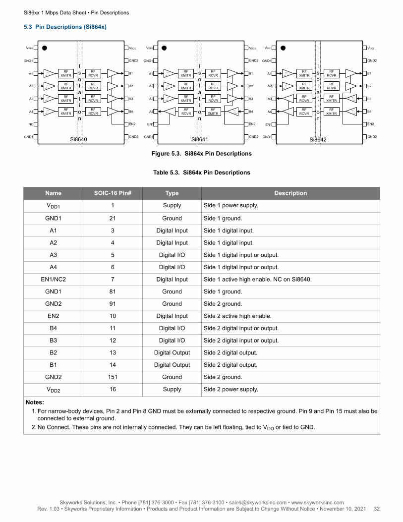
5.3 Pin Descriptions (Si864x)
VDD1
GND1
A1
A3
A4
NC
GND1
A2
VDD2
GND2
B2
B1
B4
B3
GND2
EN2
Isolat ion
RFXMITR
RFRCVR
RFXMITR
RFRCVR
RFXMITR
RFRCVR
RFXMITR
RFRCVR
Si8640
VDD1
GND1
A1
A3
A4
EN1
GND1
A2
VDD2
GND2
B2
B1
B4
B3
GND2
EN2
Isolat ion
RFXMITR
RFRCVR
RFXMITR
RFRCVR
RFXMITR
RFRCVR
RFXMITR
RFRCVR
Si8641
VDD1
GND1
A1
A3
A4
EN1
GND1
A2
VDD2
GND2
B2
B1
B4
B3
GND2
EN2
Isolat ion
RFXMITR
RFRCVR
RFXMITR
RFRCVR
RFRCVR
RFXMITR
RFRCVR
RFXMITR
RFRCVR
Si8642
Figure 5.3. Si864x Pin Descriptions
Table 5.3. Si864x Pin Descriptions
Name SOIC-16 Pin# Type Description
VDD1 1 Supply Side 1 power supply.
GND1 21 Ground Side 1 ground.
A1 3 Digital Input Side 1 digital input.
A2 4 Digital Input Side 1 digital input.
A3 5 Digital I/O Side 1 digital input or output.
A4 6 Digital I/O Side 1 digital input or output.
EN1/NC2 7 Digital Input Side 1 active high enable. NC on Si8640.
GND1 81 Ground Side 1 ground.
GND2 91 Ground Side 2 ground.
EN2 10 Digital Input Side 2 active high enable.
B4 11 Digital I/O Side 2 digital input or output.
B3 12 Digital I/O Side 2 digital input or output.
B2 13 Digital Output Side 2 digital output.
B1 14 Digital Output Side 2 digital output.
GND2 151 Ground Side 2 ground.
VDD2 16 Supply Side 2 power supply.
Notes:1. For narrow-body devices, Pin 2 and Pin 8 GND must be externally connected to respective ground. Pin 9 and Pin 15 must also be
connected to external ground.2. No Connect. These pins are not internally connected. They can be left floating, tied to VDD or tied to GND.
Si86xx 1 Mbps Data Sheet • Pin Descriptions
Skyworks Solutions, Inc. • Phone [781] 376-3000 • Fax [781] 376-3100 • [email protected] • www.skyworksinc.com32 Rev. 1.03 • Skyworks Proprietary Information • Products and Product Information are Subject to Change Without Notice • November 10, 2021 32

5.4 Pin Descriptions (Si8650/51/52)
VDD1
A1
A3
A4
NC
GND1
A2
VDD2
B2
B1
B4
B3
GND2
EN2
Isolat ion
RFXMITR
RFRCVR
RFXMITR
RFRCVR
RFXMITR
RFRCVR
RFXMITR
RFRCVR
Si8650
A5
RFXMITR
RFRCVR
B5
VDD1
A1
A3
A4
EN1
GND1
A2
VDD2
B2
B1
B4
B3
GND2
EN2
Isolat ion
RFXMITR
RFRCVR
RFXMITR
RFRCVR
RFXMITR
RFRCVR
RFXMITR
RFRCVR
Si8651
RFXMITR
RFRCVR
A5 B5
VDD1
A1
A3
A4
EN1
GND1
A2
VDD2
B2
B1
B4
B3
GND2
EN2
Isolat ion
RFXMITR
RFRCVR
RFXMITR
RFRCVR
RFRCVR
RFXMITR
RFRCVR
RFXMITR
RFRCVR
Si8652
RFXMITR
RFRCVR
A5 B5
Figure 5.4. Si865x Pin Descriptions
Table 5.4. Si865x Pin Descriptions
Name SOIC-16 Pin# Type Description
VDD1 1 Supply Side 1 power supply.
A1 2 Digital Input Side 1 digital input.
A2 3 Digital Input Side 1 digital input.
A3 4 Digital Input Side 1 digital input.
A4 5 Digital I/O Side 1 digital input or output.
A5 6 Digital I/O Side 1 digital input or output.
EN1/NC* 7 Digital Input Side 1 active high enable. NC on Si8650.
GND1 8 Ground Side 1 ground.
GND2 9 Ground Side 2 ground.
EN2 10 Digital Input Side 2 active high enable.
B5 11 Digital I/O Side 2 digital input or output.
B4 12 Digital I/O Side 2 digital input or output.
B3 13 Digital Output Side 2 digital output.
B2 14 Digital Output Side 2 digital output.
B1 15 Digital Output Side 2 digital output.
VDD2 16 Supply Side 2 power supply.
Note: No Connect. These pins are not internally connected. They can be left floating, tied to VDD or tied to GND.
Si86xx 1 Mbps Data Sheet • Pin Descriptions
Skyworks Solutions, Inc. • Phone [781] 376-3000 • Fax [781] 376-3100 • [email protected] • www.skyworksinc.com33 Rev. 1.03 • Skyworks Proprietary Information • Products and Product Information are Subject to Change Without Notice • November 10, 2021 33
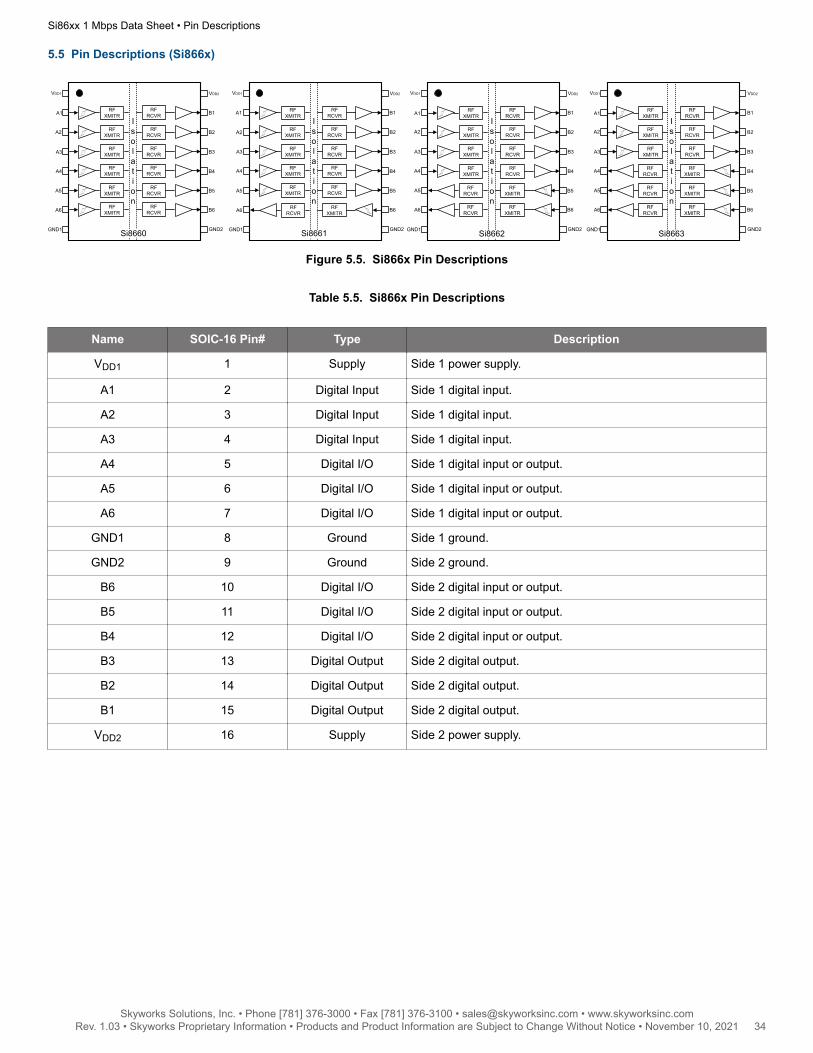
5.5 Pin Descriptions (Si866x)
VDD1
A1
A3
A4
GND1
A2
VDD2
B2
B1
B4
B3
GND2
Isolat ion
RFXMITR
RFRCVR
RFXMITR
RFRCVR
RFXMITR
RFRCVR
RFXMITR
RFRCVR
Si8660
A5
RFXMITR
RFRCVR
B5
B6A6 RFXMITR
RFRCVR
VDD1
A1
A3
A4
GND1
A2
VDD2
B2
B1
B4
B3
GND2
Isolat ion
RFXMITR
RFRCVR
RFXMITR
RFRCVR
RFXMITR
RFRCVR
Si8661
RFXMITR
RFRCVR
A5 B5
RFXMITR
RFRCVR
B6A6
RFXMITR
RFRCVR
VDD1
A1
A3
A4
GND1
A2
VDD2
B2
B1
B4
B3
GND2
Isolat ion
RFXMITR
RFRCVR
RFXMITR
RFRCVR
RFRCVR
RFXMITR
RFRCVR
RFXMITR
RFRCVR
Si8662
RFXMITR
RFRCVR
A5 B5
B6A6
RFXMITR
RFRCVR
VDD1
A1
A3
A4
GND1
A2
VDD2
B2
B1
B4
B3
GND2
Isolat ion
RFXMITR
RFRCVR
RFXMITR
RFRCVR
RFRCVR
RFXMITR
RFRCVR
RFXMITR
RFRCVR
Si8663
RFXMITR
RFRCVR
A5 B5
B6A6
RFXMITR
RFRCVR
Figure 5.5. Si866x Pin Descriptions
Table 5.5. Si866x Pin Descriptions
Name SOIC-16 Pin# Type Description
VDD1 1 Supply Side 1 power supply.
A1 2 Digital Input Side 1 digital input.
A2 3 Digital Input Side 1 digital input.
A3 4 Digital Input Side 1 digital input.
A4 5 Digital I/O Side 1 digital input or output.
A5 6 Digital I/O Side 1 digital input or output.
A6 7 Digital I/O Side 1 digital input or output.
GND1 8 Ground Side 1 ground.
GND2 9 Ground Side 2 ground.
B6 10 Digital I/O Side 2 digital input or output.
B5 11 Digital I/O Side 2 digital input or output.
B4 12 Digital I/O Side 2 digital input or output.
B3 13 Digital Output Side 2 digital output.
B2 14 Digital Output Side 2 digital output.
B1 15 Digital Output Side 2 digital output.
VDD2 16 Supply Side 2 power supply.
Si86xx 1 Mbps Data Sheet • Pin Descriptions
Skyworks Solutions, Inc. • Phone [781] 376-3000 • Fax [781] 376-3100 • [email protected] • www.skyworksinc.com34 Rev. 1.03 • Skyworks Proprietary Information • Products and Product Information are Subject to Change Without Notice • November 10, 2021 34

6. Package Outlines
6.1 Package Outline (16-Pin Wide Body SOIC)
The figure below illustrates the package details for the Si86xx Digital Isolator. The table below lists the values for the dimensions shownin the illustration.
Figure 6.1. 16-Pin Wide Body SOIC
Si86xx 1 Mbps Data Sheet • Package Outlines
Skyworks Solutions, Inc. • Phone [781] 376-3000 • Fax [781] 376-3100 • [email protected] • www.skyworksinc.com35 Rev. 1.03 • Skyworks Proprietary Information • Products and Product Information are Subject to Change Without Notice • November 10, 2021 35

Table 6.1. Package Diagram Dimensions
Dimension Min Max
A — 2.65
A1 0.10 0.30
A2 2.05 —
b 0.31 0.51
c 0.20 0.33
D 10.30 BSC
E 10.30 BSC
E1 7.50 BSC
e 1.27 BSC
L 0.40 1.27
h 0.25 0.75
θ 0° 8°
aaa — 0.10
bbb — 0.33
ccc — 0.10
ddd — 0.25
eee — 0.10
fff — 0.20
Notes:1. All dimensions shown are in millimeters (mm) unless otherwise noted.2. Dimensioning and Tolerancing per ANSI Y14.5M-1994.3. This drawing conforms to JEDEC Outline MS-013, Variation AA.4. Recommended reflow profile per JEDEC J-STD-020 specification for small body, lead-free components.
Si86xx 1 Mbps Data Sheet • Package Outlines
Skyworks Solutions, Inc. • Phone [781] 376-3000 • Fax [781] 376-3100 • [email protected] • www.skyworksinc.com36 Rev. 1.03 • Skyworks Proprietary Information • Products and Product Information are Subject to Change Without Notice • November 10, 2021 36
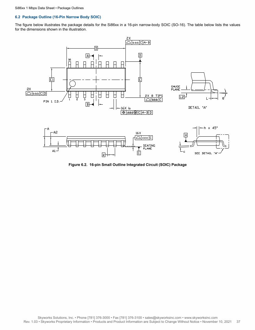
6.2 Package Outline (16-Pin Narrow Body SOIC)
The figure below illustrates the package details for the Si86xx in a 16-pin narrow-body SOIC (SO-16). The table below lists the valuesfor the dimensions shown in the illustration.
Figure 6.2. 16-pin Small Outline Integrated Circuit (SOIC) Package
Si86xx 1 Mbps Data Sheet • Package Outlines
Skyworks Solutions, Inc. • Phone [781] 376-3000 • Fax [781] 376-3100 • [email protected] • www.skyworksinc.com37 Rev. 1.03 • Skyworks Proprietary Information • Products and Product Information are Subject to Change Without Notice • November 10, 2021 37

Table 6.2. Package Diagram Dimensions
Dimension Min Max
A — 1.75
A1 0.10 0.25
A2 1.25 —
b 0.31 0.51
c 0.17 0.25
D 9.90 BSC
E 6.00 BSC
E1 3.90 BSC
e 1.27 BSC
L 0.40 1.27
L2 0.25 BSC
h 0.25 0.50
θ 0° 8°
aaa 0.10
bbb 0.20
ccc 0.10
ddd 0.25
Notes:1. All dimensions shown are in millimeters (mm) unless otherwise noted.2. Dimensioning and Tolerancing per ANSI Y14.5M-1994.3. This drawing conforms to the JEDEC Solid State Outline MS-012, Variation AC.4. Recommended card reflow profile is per the JEDEC/IPC J-STD-020 specification for Small Body Components.
Si86xx 1 Mbps Data Sheet • Package Outlines
Skyworks Solutions, Inc. • Phone [781] 376-3000 • Fax [781] 376-3100 • [email protected] • www.skyworksinc.com38 Rev. 1.03 • Skyworks Proprietary Information • Products and Product Information are Subject to Change Without Notice • November 10, 2021 38

6.3 Package Outline (8-Pin Narrow Body SOIC)
The figure below illustrates the package details for the Si86xx. The table below lists the values for the dimensions shown in theillustration.
α
Figure 6.3. 8-pin Small Outline Integrated Circuit (SOIC) Package
Table 6.3. Package Diagram Dimensions
Symbol Millimeters
Min Max
A 1.35 1.75
A1 0.10 0.25
A2 1.40 REF 1.55 REF
B 0.33 0.51
C 0.19 0.25
D 4.80 5.00
E 3.80 4.00
e 1.27 BSC
H 5.80 6.20
h 0.25 0.50
L 0.40 1.27
∝ 0° 8°
Si86xx 1 Mbps Data Sheet • Package Outlines
Skyworks Solutions, Inc. • Phone [781] 376-3000 • Fax [781] 376-3100 • [email protected] • www.skyworksinc.com39 Rev. 1.03 • Skyworks Proprietary Information • Products and Product Information are Subject to Change Without Notice • November 10, 2021 39

7. Land Patterns
7.1 Land Pattern (16-Pin Wide-Body SOIC)
The figure below illustrates the recommended land pattern details for the Si86xx in a 16-pin wide-body SOIC. The table below lists thevalues for the dimensions shown in the illustration.
Figure 7.1. 16-Pin SOIC Land Pattern
Table 7.1. 16-Pin Wide Body SOIC Land Pattern Dimensions
Dimension Feature (mm)
C1 Pad Column Spacing 9.40
E Pad Row Pitch 1.27
X1 Pad Width 0.60
Y1 Pad Length 1.90
Notes:1. This Land Pattern Design is based on IPC-7351 pattern SOIC127P1032X265-16AN for Density Level B (Median Land Protru-
sion).2. All feature sizes shown are at Maximum Material Condition (MMC) and a card fabrication tolerance of 0.05 mm is assumed.
Si86xx 1 Mbps Data Sheet • Land Patterns
Skyworks Solutions, Inc. • Phone [781] 376-3000 • Fax [781] 376-3100 • [email protected] • www.skyworksinc.com40 Rev. 1.03 • Skyworks Proprietary Information • Products and Product Information are Subject to Change Without Notice • November 10, 2021 40

7.2 Land Pattern (16-Pin Narrow Body SOIC)
The figure below illustrates the recommended land pattern details for the Si86xx in a 16-pin narrow-body SOIC. The table below liststhe values for the dimensions shown in the illustration.
Figure 7.2. 16-Pin Narrow Body SOIC PCB Land Pattern
Table 7.2. 16-Pin Narrow Body SOIC Land Pattern Dimensions
Dimension Feature (mm)
C1 Pad Column Spacing 5.40
E Pad Row Pitch 1.27
X1 Pad Width 0.60
Y1 Pad Length 1.55
Notes:1. This Land Pattern Design is based on IPC-7351 pattern SOIC127P600X165-16N for Density Level B (Median Land Protrusion).2. All feature sizes shown are at Maximum Material Condition (MMC) and a card fabrication tolerance of 0.05 mm is assumed.
Si86xx 1 Mbps Data Sheet • Land Patterns
Skyworks Solutions, Inc. • Phone [781] 376-3000 • Fax [781] 376-3100 • [email protected] • www.skyworksinc.com41 Rev. 1.03 • Skyworks Proprietary Information • Products and Product Information are Subject to Change Without Notice • November 10, 2021 41

7.3 Land Pattern (8-Pin Narrow Body SOIC)
The figure below illustrates the recommended land pattern details for the Si86xx in an 8-pin narrow-body SOIC. The table below liststhe values for the dimensions shown in the illustration.
Figure 7.3. PCB Land Pattern: 8-Pin Narrow Body SOIC
Table 7.3. PCM Land Pattern Dimensions (8-Pin Narrow Body SOIC)
Dimension Feature (mm)
C1 Pad Column Spacing 5.40
E Pad Row Pitch 1.27
X1 Pad Width 0.60
Y1 Pad Length 1.55
Notes:1. This Land Pattern Design is based on IPC-7351 pattern SOIC127P600X173-8N for Density Level B (Median Land Protrusion).2. All feature sizes shown are at Maximum Material Condition (MMC) and a card fabrication tolerance of 0.05 mm is assumed.
Si86xx 1 Mbps Data Sheet • Land Patterns
Skyworks Solutions, Inc. • Phone [781] 376-3000 • Fax [781] 376-3100 • [email protected] • www.skyworksinc.com42 Rev. 1.03 • Skyworks Proprietary Information • Products and Product Information are Subject to Change Without Notice • November 10, 2021 42

8. Top Markings
8.1 Top Marking (16-Pin Wide Body SOIC)
Si86XYSVYYWWRTTTTT
CC e4
Figure 8.1. 16-Pin Wide Body SOIC
Table 8.1. Top Marking Explanation (16-Pin Wide Body SOIC)
Line 1 Marking: Base Part Number
Ordering Options
(See 1. Ordering Guide for more information).
Si86 = Isolator product series
XY = Channel Configuration
X = # of data channels (5, 4, 3, 2, 1)
Y = # of reverse channels (2, 1, 0)
S = Speed Grade (max data rate) and operating mode:
A = 1 Mbps (default output = low)
B = 150 Mbps (default output = low)
D = 1 Mbps (default output = high)
E = 150 Mbps (default output = high)
V = Insulation rating
A = 1 kV; B = 2.5 kV; C = 3.75 kV; D = 5.0 kV
Line 2 Marking: YY = Year
WW = Workweek
Assigned by assembly subcontractor. Corresponds to the yearand work week of the mold date.
RTTTTT = Mfg Code Manufacturing code from assembly house
“R” indicates revision
Line 3 Marking: Circle = 1.7 mm Diameter
(Center-Justified)
“e4” Pb-free symbol
Country of Origin ISO Code Abbreviation CC = Country of Origin ISO Code Abbreviation• TW = Taiwan• TH = Thailand
Si86xx 1 Mbps Data Sheet • Top Markings
Skyworks Solutions, Inc. • Phone [781] 376-3000 • Fax [781] 376-3100 • [email protected] • www.skyworksinc.com43 Rev. 1.03 • Skyworks Proprietary Information • Products and Product Information are Subject to Change Without Notice • November 10, 2021 43

8.2 Top Marking (16-Pin Narrow Body SOIC)
Si86XYSVYYWWRTTTTT e3
Figure 8.2. 16-Pin Narrow Body SOIC
Table 8.2. Top Marking Explanation (16-Pin Narrow Body SOIC)
Line 1 Marking: Base Part Number
Ordering Options
(See 1. Ordering Guide for more information.)
Si86 = Isolator product series
XY = Channel Configuration
X = # of data channels (5, 4, 3, 2, 1)
Y = # of reverse channels (2, 1, 0)
S = Speed Grade (max data rate) and operating mode:
A = 1 Mbps (default output = low)
B = 150 Mbps (default output = low)
D = 1 Mbps (default output = high)
E = 150 Mbps (default output = high)
V = Insulation rating
A = 1 kV; B = 2.5 kV; C = 3.75 kV
Line 2 Marking: Circle = 1.2 mm Diameter “e3” Pb-Free Symbol
YY = Year
WW = Work Week
Assigned by the assembly subcontractor. Corresponds to theyear and work week of the mold date.
RTTTTT = Mfg Code Manufacturing code from assembly house
“R” indicates revision
Si86xx 1 Mbps Data Sheet • Top Markings
Skyworks Solutions, Inc. • Phone [781] 376-3000 • Fax [781] 376-3100 • [email protected] • www.skyworksinc.com44 Rev. 1.03 • Skyworks Proprietary Information • Products and Product Information are Subject to Change Without Notice • November 10, 2021 44

8.3 Top Marking (8-Pin Narrow Body SOIC)
Si86XYSVYYWWRT
TTTT e3
Figure 8.3. 8-Pin Narrow Body SOIC
Table 8.3. Top Marking Explanation (8-Pin Narrow Body SOIC)
Line 1 Marking: Base Part Number
Ordering Options
(See 1. Ordering Guide for more information).
Si86 = Isolator Product Series
XY = Channel Configuration
S = Speed Grade (max data rate)
V = Insulation rating
Line 2 Marking: YY = Year
WW = Workweek
Assigned by assembly subcontractor. Corresponds to the yearand workweek of the mold date.
R = Product Revision
T = First character of the manufacturing code
Line 3 Marking: Circle = 1.1 mm Diameter “e3” Pb-Free Symbol.
TTTT = Last four characters of the manufactur-ing code
Last four characters of the manufacturing code.
Si86xx 1 Mbps Data Sheet • Top Markings
Skyworks Solutions, Inc. • Phone [781] 376-3000 • Fax [781] 376-3100 • [email protected] • www.skyworksinc.com45 Rev. 1.03 • Skyworks Proprietary Information • Products and Product Information are Subject to Change Without Notice • November 10, 2021 45

9. Revision History
Revision 1.03
September 2019• Updated Ordering Guide.
Revision 1.02
February 2018• Added SI8641AB-AS1 and SI8642AB-AS1 to Ordering Guide for Automotive-Grade OPN options
Revision 1.01
January 2018• Updated data sheet format.• Added new table to Ordering Guide for Automotive-Grade OPN options
• Updated Table 4.5 Regulatory Information1 on page 25.• Added CQC certificate numbers.
• Updated 1. Ordering Guide.• Removed references to moisture sensitivity levels.• Removed note 2.
Si86xx 1 Mbps Data Sheet • Revision History
Skyworks Solutions, Inc. • Phone [781] 376-3000 • Fax [781] 376-3100 • [email protected] • www.skyworksinc.com46 Rev. 1.03 • Skyworks Proprietary Information • Products and Product Information are Subject to Change Without Notice • November 10, 2021 46

Copyright © 2021 Skyworks Solutions, Inc. All Rights Reserved.Information in this document is provided in connection with Skyworks Solutions, Inc. (“Skyworks”) products or services. These materials, including the information contained herein, are provided by Skyworks as a service to its customers and may be used for informational purposes only by the customer. Skyworks assumes no responsibility for errors or omissions in these materials or the information contained herein. Skyworks may change its documentation, products, services, specifications or product descriptions at any time, without notice. Skyworks makes no commitment to update the materials or information and shall have no responsibility whatsoever for conflicts, incompatibilities, or other difficulties arising from any future changes.
No license, whether express, implied, by estoppel or otherwise, is granted to any intellectual property rights by this document. Skyworks assumes no liability for any materials, products or information provided hereunder, including the sale, distribution, reproduction or use of Skyworks products, information or materials, except as may be provided in Skyworks’ Terms and Conditions of Sale.
THE MATERIALS, PRODUCTS AND INFORMATION ARE PROVIDED “AS IS” WITHOUT WARRANTY OF ANY KIND, WHETHER EXPRESS, IMPLIED, STATUTORY, OR OTHERWISE, INCLUDING FITNESS FOR A PARTICULAR PURPOSE OR USE, MERCHANTABILITY, PERFORMANCE, QUALITY OR NON-INFRINGEMENT OF ANY INTELLECTUAL PROPERTY RIGHT; ALL SUCH WARRANTIES ARE HEREBY EXPRESSLY DISCLAIMED. SKYWORKS DOES NOT WARRANT THE ACCURACY OR COMPLETENESS OF THE INFORMATION, TEXT, GRAPHICS OR OTHER ITEMS CONTAINED WITHIN THESE MATERIALS. SKYWORKS SHALL NOT BE LIABLE FOR ANY DAMAGES, INCLUDING BUT NOT LIMITED TO ANY SPECIAL, INDIRECT, INCIDENTAL, STATUTORY, OR CONSEQUENTIAL DAMAGES, INCLUDING WITHOUT LIMITATION, LOST REVENUES OR LOST PROFITS THAT MAY RESULT FROM THE USE OF THE MATERIALS OR INFORMATION, WHETHER OR NOT THE RECIPIENT OF MATERIALS HAS BEEN ADVISED OF THE POSSIBILITY OF SUCH DAMAGE.
Skyworks products are not intended for use in medical, lifesaving or life-sustaining applications, or other equipment in which the failure of the Skyworks products could lead to personal injury, death, physical or environmental damage. Skyworks customers using or selling Skyworks products for use in such applications do so at their own risk and agree to fully indemnify Skyworks for any damages resulting from such improper use or sale.
Customers are responsible for their products and applications using Skyworks products, which may deviate from published specifications as a result of design defects, errors, or operation of products outside of published parameters or design specifications. Customers should include design and operating safeguards to minimize these and other risks. Skyworks assumes no liability for applications assistance, customer product design, or damage to any equipment resulting from the use of Skyworks products outside of Skyworks’ published specifications or parameters.
Skyworks, the Skyworks symbol, Sky5®, SkyOne®, SkyBlue™, Skyworks Green™, Clockbuilder®, DSPLL®, ISOmodem®, ProSLIC®, and SiPHY® are trademarks or registered trademarks of Skyworks Solutions, Inc. or its subsidiaries in the United States and other countries. Third-party brands and names are for identification purposes only and are the property of their respective owners. Additional information, including relevant terms and conditions, posted at www.skyworksinc.com, are incorporated by reference.
Portfoliowww.skyworksinc.com
Qualitywww.skyworksinc.com/quality
Support & Resourceswww.skyworksinc.com/support
Connecting Everyone
and Everything,
All the Time
Skyworks Solutions, Inc. | Nasdaq: SWKS | [email protected] | www.skyworksinc.comUSA: 781-376-3000 | Asia: 886-2-2735 0399 | Europe: 33 (0)1 43548540 |