Si477X AYOUT GUIDELINES 1. Si477x QFN 6x6 mm Schematic …
15
Rev. 0.3 8/13 Copyright © 2012 by Silicon Laboratories AN644 AN644 Si477 X L AYOUT G UIDELINES 1. Si477x QFN 6x6 mm Schematic and Layout This section describes the application schematic and layout required for optimal Si477x performance. 1.1. Front-End Schematic Figure 1. Si477x FM/AM Front-End Schematic NP J36 NP J37 RF RF RF RF RF J29 37.20 C7 2.2NF RF T1 4 2 3 1 6 1:1 RF NP C22 C8 1NF C9 62PF L1 220NH L3 150NH J1 SMA_EDGE RF NP C23 41 40 39 38 12 11 10 9 8 7 6 5 4 3 2 1 FMXIP FMXIN GNDRF RFREG FMO FMI NC AMI A0 A1 FMAGC2 FMAGC1 GND_PAD NC NC T2 5 4 3 1 SL755TF01 SILABS R1 0R R4 0 L2 47NH C10 18PF JP1 D1 ESD_DIODE 10UF C6 10NH L9 D3 ESD_DIODE RF RF 0.1UF C13 J33 SMA_EDGE RF RF D2 ESD_DIODE 0R J35 0 R5 C24 NP C25 NP C26 NP RF NP C27 RF RF RF RF RF C11 NP GND AIRLOOP ANT FM ANT AM ANT
Transcript of Si477X AYOUT GUIDELINES 1. Si477x QFN 6x6 mm Schematic …

Rev. 0.3 8/13 Copyright © 2012 by Silicon Laboratories AN644
AN644
Si477X LAYOUT GUIDELINES
1. Si477x QFN 6x6 mm Schematic and Layout
This section describes the application schematic and layout required for optimal Si477x performance.
1.1. Front-End Schematic
Figure 1. Si477x FM/AM Front-End Schematic
NP
J36
NP
J37
RF
RF
RF
RF
RF
J29
37.20
C72.2NF
RF
T1
4
2
3
1 61:1RFNP
C22
C81NF
C962PF
L1220NH
L3150NH
J1
SMA_EDGE
RF
NPC23
41
40 39 381211
10987654321
FMXIPFMXINGNDRFRFREGFMOFMI
NCAMI
A0
A1
FMA
GC
2FM
AG
C1
GN
D_P
AD
NC
NC
T2
5
4 3
1
SL755TF01SILABS
R1
0R
R4
0
L247NH
C1018PF
JP1
D1ESD_DIODE
10UFC6
10NHL9
D3 ESD_DIODE
RF
RF
0.1UFC13
J33
SMA_EDGE
RF
RF
D2ESD_DIODE
0R J35
0
R5
C24NP
C25NP
C26NP
RF
NPC27
RF
RF
RF
RF
RF
C11NP
GNDAIRLOOP ANT
FM ANT
AM ANT

AN644
2 Rev. 0.3
1.2. Front-End Layout
The following layout rules are used:
Layer 1 top side component placement and analog signal routing
Layer 2 solid ground plane
Layer 3 digital signal routing
Layer 4 solid ground plane
Power routed by trace
0402 component size or larger
6 mil traces
6 mil trace spacing
15 mil component spacing
Figure 2. Four-Layer PCB Stackup
Figure 3. Si477x FM/AM Front-End Layout

AN644
Rev. 0.3 3
1.3. FM Front-End1.3.1. FM Front-End
ESD diode D1 protects against external antenna ESD events. Place D1 close to the antenna connector. Choosediodes with minimum parasitic capacitance, such as the Tyco Electronics PESD0402-140 (0.25 pF).
Series inductor L9 (10 nH) suppresses EMI.
The AM loading capacitor, C10 (18 pF) ac-couples the antenna to the input network and resonates with theinductor L3 (150 nH).
The FM input (FMI, Pin 7) matching network consists of L2 (47 nH), C9 (62 pF), and AGC-controlled internalresistor banks FMAGC1 (Pin 40) and FMAGC2 (Pin 39). Place these components close to the FMAGC1/2 pins tominimize trace inductance. Connect FMI using two vias and a trace on PCB Layer 2.
Connect the LNA output (FMO, Pin 6) to the RF regulator (RFREG, Pin 5) using L1 (220 nH). Place L1 and RFregulator bypass capacitor C7 (2.2 nF) close the RFREG pin.
Connect the LNA output through ac-coupling capacitor C8 (1 nF) to input of T1, the external FM balun. The twooutputs of the balun are connected to FM mixer inputs (FMXIP, Pin 2 and FMXIN, Pin 3).
Shunt Capacitors C11,C22, C24, C25, and C26 are placeholders for filtering caps on the EVB. They may not berequired in actual application.
Components should be placed close to the IC to minimize trace lengths.
All front-end ground connections should be to a common system ground. Alternatively, an RF ground plane shouldbe connected to system ground by a shield or large copper fill.
1.3.2. AM Front-End
The schematic shows two paths to the AM input (AMI, pin 10). The path originating with J33 is used on theevaluation board for conducted testing and is not needed as part of the true application circuit. The path originatingfrom JP1 assumes a loop antenna will be used. JP1 is connected to an external AM transformer (T2).
The output of the transformer is ac coupled to the AMI input pin through a 0.1 uF capacitor (C13).
Ensure R5 is populated for loop antenna reception and J35 is shorted for conducted tests. The output of C13 isconnected to the AMI input pin. Components should be placed close to the IC to minimize trace lengths.
Shunt Capacitors C23 and C27 are placeholders for filtering caps on the EVB. They may not be required in actualapplication.

AN644
4 Rev. 0.3
1.4. System Interface Schematic
Figure 4. Si477x System Interface Schematic
RF
C12NP
J32J29
X137.209375MHZ
3.2x
2.5
NF
4
6
U1
41
40 39 38 37 36 35 34 33 32 3130292827262524232221
20191817161514131211
10987654321
FMXIPFMXINGNDRFRFREGFMOFMI
NCAMI
A0
A1
RS
TBS
DA
SC
LIN
TBV
IO1
VD
DBYPVIO2IQCLKIQFSIOUTQOUTDOUTDFSDCLK
VA
LOU
TR
OU
TX
TAL2
XTA
L1D
AC
RE
FG
PIO
2G
PIO
1FM
AG
C2
FMA
GC
1
GN
D_P
AD
DC
LK2
DO
UT2
NC
NC BLEND
SI477X
C5 2.2NF
100PFC1 C2
2.2NF
C32.2NF
C2010UF
C42.2NF
10UFC6
0.1UFC21
VD
VA
IQCLK
V_PGM
XOUT
LOUT
XIN
VIO2
GPIO_3
DCLK
QOUT
VIO1
DOUTDFS
ROUT
IOUTIQFS
INTB_1SCL
RSTB_1
GPIO_0
SDA
GPIO_1
GPIO_2
D_0
AN644
Rev. 0.3 5
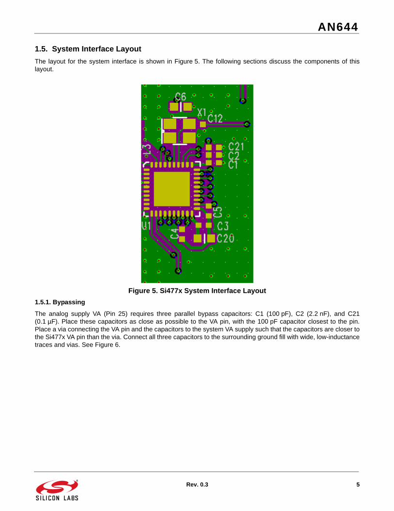
1.5. System Interface Layout
The layout for the system interface is shown in Figure 5. The following sections discuss the components of thislayout.
Figure 5. Si477x System Interface Layout
1.5.1. Bypassing
The analog supply VA (Pin 25) requires three parallel bypass capacitors: C1 (100 pF), C2 (2.2 nF), and C21(0.1 µF). Place these capacitors as close as possible to the VA pin, with the 100 pF capacitor closest to the pin.Place a via connecting the VA pin and the capacitors to the system VA supply such that the capacitors are closer tothe Si477x VA pin than the via. Connect all three capacitors to the surrounding ground fill with wide, low-inductancetraces and vias. See Figure 6.

AN644
6 Rev. 0.3
Figure 6. Si477x VA Supply Bypassing Layout
The voltage reference for the audio DAC (DACREF, Pin 36) requires a 10 µF capacitor (C6) to ground. Both VAand DACREF bypassing should be connected to the system ground plane.
The digital supply VD (Pin 20) requires two parallel bypass capacitors, C3 (2.2 nF), and C20 (10 µF). Place thesecapacitors as close as possible to the VD pin, with the 2.2 nF capacitor closest to the pin. Place a via connectingthe VD pin and the capacitors to the system VD supply such that the capacitors are closer to the Si477x VD pinthan the via. See Figure 7, “Si477x VD/VIO1/VIO2 Supply Bypassing Layout”.
The control (VIO1, Pin 19) and data bus interface (VIO2, Pin 22) supplies each require a 2.2 nF bypass capacitor(C4, C5). Place each capacitor as close as possible to the corresponding VIO pin. Place a via connecting the VIOpin and the capacitor to the system VIO supply such that the capacitor is closer to the Si477x VIO pin than the via.
Connect all digital bypass capacitors (C3, C20, C4, C5) only to the digital bypass ground (DBYP) Pin 21 with awide, low-inductance trace. Do not connect the digital bypassing capacitors to the PCB ground; this grounding isprovided by the Si477x internally. See Figure 7, “Si477x VD/VIO1/VIO2 Supply Bypassing Layout”.
DACREF bypass capacitor location
VA supply VIA location
VA bypass capacitor location and ground fill

AN644
Rev. 0.3 7
Figure 7. Si477x VD/VIO1/VIO2 Supply Bypassing Layout
1.5.2. Reference Clock
The Si477x generates all internal clocking from an external crystal using an on-chip oscillator or an external refer-ence clock. The supported crystal and external clock source frequency is 4 MHz. The reference clock/crystal accu-racy must be within ±100 ppm.
X1 is an optional crystal required only when using the internal oscillator feature. Place the crystal, X1, as close toXTAL1 (Pin 35) and XTAL2 (Pin 34) as possible to minimize current loop lengths. If an external clock source isused instead of a crystal, route the clock through series capacitor C12 to XTAL2 and leave XTAL1 floating (NC).Route the RCLK trace as far away from digital I/O traces as possible to minimize capacitive coupling.
1.5.3. Analog Audio / MPX Output (Si4777)
High-fidelity digital-to-analog converters (DACs) drive analog audio signals or the FM MPX signal to LOUT/MPX-OUT (Pin 32) and ROUT (Pin 33). For analog audio and FM MPX information, refer to the Si477x data sheet.
Location of digital bypass capacitors

AN644
8 Rev. 0.3
1.5.4. Control Interface
All control interface signals operate at VIO1 supply levels. Route all control interface traces on Layer 2 to minimize
coupling to the RF front-end. SDA and SCL (Pins 16 and 17) are an I2C-compatible serial port slave interface,which allows an external controller to send commands and receive responses from the Si477x. Both the SDA andSCL signals require external pull-up resistors to VIO1. The value of pull-up resistor values will vary based on the
number of devices, capacitance, and speed of the bus. Placement location is not critical. Refer to the I2C specifica-
tion for additional design information. For I2C Control Bus information, refer to the Si477x data sheet.
A0 and A1 (Pins 11 and 12) select the I2C device address. Leave each pin either floating (NC) or connected to the
system ground. For I2C Device Address selection, refer to the Si477x data sheet.
RSTB (Pin 15) is the global chip reset input. Setting the RSTB pin low disables analog and digital circuitry, resetsthe registers to their default settings, and disables the bus. Setting the RSTB pin high brings the device out ofreset. For Reset, Powerup, and Powerdown information, refer to the Si477x data sheet.
INTB (Pin 18) is an active low interrupt output. See “AN645:Si477x Programming Guide” for interrupt configuration.
Series termination resistors may be added to the SDA, SCL, and INTB traces to mitigate system noise and controlslew rate. Confirm that data sheet timing requirements are met with the selected series termination resistor value.Place the series termination resistors for SDA and INTB as close to the Si477x as possible. Place the series termi-nation resistor for SCL close to the host controller.
1.5.5. Digital Audio Interface
The digital audio interface includes data serial lines containing audio data (DOUT, Pin 27), a bit clock (DCLK, Pin29), and a word frame for left- and right-channel data (DFS, Pin 28). For Digital Audio Interface information, refer tothe Si477x data sheet.
All digital audio signals operate at VIO2 supply levels. Route all digital audio traces on Layer 3 to minimize couplingto the RF front-end.
Series termination resistors may be added to the DOUT, DCLK, and DFS traces to mitigate system noise andcontrol slew rate. Confirm that data sheet timing requirements are met with the selected series termination resistorvalue. Place the series termination resistors for DCLK and DFS as close to the host controller as possible. Placethe series termination resistor for DOUT close to the Si477x.

AN644
Rev. 0.3 9
1.5.6. Digital I/Q ZIF Output and IBOC Blend Mode (Si4777)
All digital I/Q signals operate at VIO2 supply levels. Route all digital I/Q traces on Layer 3 to minimize coupling tothe RF front-end.
The digital ZIF I/Q output provides the down-converted channelized AM/FM signal at baseband to a third-party pro-cessor for IBOC signal processing. The ZIF I/Q 4-pin interface consists of two data serial lines containing I and Qdata (IOUT/QOUT, Pins 25/26), a bit clock (IQCLK, Pin 23), and a word frame for each data sample (IQFS, Pin 24).Connect these traces to the I/Q input of the HD Radio Demod.
In IBOC Blend Mode (Si4777), Pins 27 through 30 (DOUT, DFS, DCLK, XOUT) are digital audio and blend controlinputs. Connect these pins to a third-party processor's digital audio master output and blend control output. Pins13, 14, and 18 (DCLK2, DOUT2, and DFS2) are blended digital audio outputs. Connect these pins to a digital audiomaster host processor. See the Si477x data sheet, section “4.12 IBOC Blend Mode for HD Radio”. The HD systemimplementation is shown below in Figure 8.
Figure 8. System Implementation of HD-Radio Reception with IBOC Blend
DSP
HD Radio Demod
Aud
io
pro
cess
ing
DemodAudio /DataDecoders
PLL
X
Si4777
Digital I/Q ZIF (I2S)
IBOC blend
Blend Flag
Blended audio
AM/FM Analog demodulationWeak signal processing
QOUT (Pin 26)IOUT (Pin 25)IQFS (Pin24)IQCLK (Pin 23)
Master
Digital frame sync
Digital bit clock
HD audio (MP1)
DOUT2 (Pin 14)
Master
AM/FM audio
4-wire mode
3-wire mode
Master
DCLK2 (Pin 13)
BLEND (Pin 30)
DCLK (Pin 29)
DFS (Pin 28)DIN (Pin 27)
DFS2 (Pin 18) Digital frame sync
Digital bit clock
ASRC
ASRCBlended
audio

AN644
10 Rev. 0.3
1.6. Thermal Performance for Two-Layer Module Applications
When designing a small, two-layer based on the Si477x, the module size must be no less than 3 x 5 cm to achievebest thermal performance, as a larger board area dissipates heat more readily. Place all LDOs on the base board ifpossible, to eliminate heat sources on the module. Lowering VA from 5.0 V to 4.8 V decreases board temperaturewithout RF performance degradation.
Connect the IC ground paddle to the bottom layer PCB ground using vias to dissipate heat. Place large vias on theground paddle connected to the bottom layer ground as shown in Figure 9. Do not use vias with diameter greaterthan 20 mils, as this may impact RF performance. Standard 1 mil via plating lowers thermal resistance and helpsdecrease temperature.
Figure 9. Si477x Ground Paddle Via Placement
Connect NC pins, I2C address select pins A0/A1, and the IC ground paddle to the top layer ground with solidground fill to lower thermal resistance.
For two-layer module designs, 2 oz Cu weight (70 µm) is required to maximize thermal performance. FR4-370HRPCB material is recommended for best thermal and RF performance due to its thermal conductivity.

AN644
Rev. 0.3 11
1.7. Design Checklist*Place VA bypass capacitors C1, C2, and C21 as close as possible to the Si477x supply pin.
Place VD bypass capacitors C3 and C20 as close as possible to the Si477x supply and digital bypass (DBYP) pins.
Place VIO1/VIO2 bypass capacitors C4 and C5 as close as possible to the Si477x supply and digital bypass pins (DBYP).
Route supplies using wide, low-inductance traces. Ensure that each trace is rated to handle the required current.
Route all supply connections through a via such that the bypass capacitors are closer to the Si477x supply pins than the source via.
Place crystal X1 as close as possible to the Si477x XTAL1/XTAL2 pins.
Select a crystal with accuracy of ±100 ppm.
Place the Si477x close to the antenna connector to minimize RF front-end trace lengths and capacitance and to minimize inductive and capacitive coupling.
Route all traces to minimize inductive and capacitive coupling by keeping digital traces away from analog and RF traces, minimizing trace length, minimizing parallel trace runs, and keeping current loops small.
Route digital traces between ground planes for best performance.
Add series termination resistors to digital signals if necessary to mitigate noise coupling. Ensure timing specifications are maintained when adding series terminations.
Connect the Si477x ground pad to the ground plane using multiple vias to minimize ground potential differences and achieve optimal thermal performance.
Do not route signal traces under the Si477x.
Do not route digital or RF traces over breaks in the ground plane.
Flood the primary and secondary routing layers with separated RF and system grounds, and connect all layers using stitching vias.
PCB size should be no less than 3 x 5 cm in a two-layer module application. Use 2 oz Cu and FR4-370 PCB material for best thermal performance.
Place 20-mil diameter vias at the IC ground paddle to for heat dissipation.
Use NC pins and I2C address lines pins 9-10 to connect ground paddle to top layer ground. The ground area should be as large as possible with many ground vias on it.
*Note: Design checklist is listed in order of importance.
AN644
12 Rev. 0.3
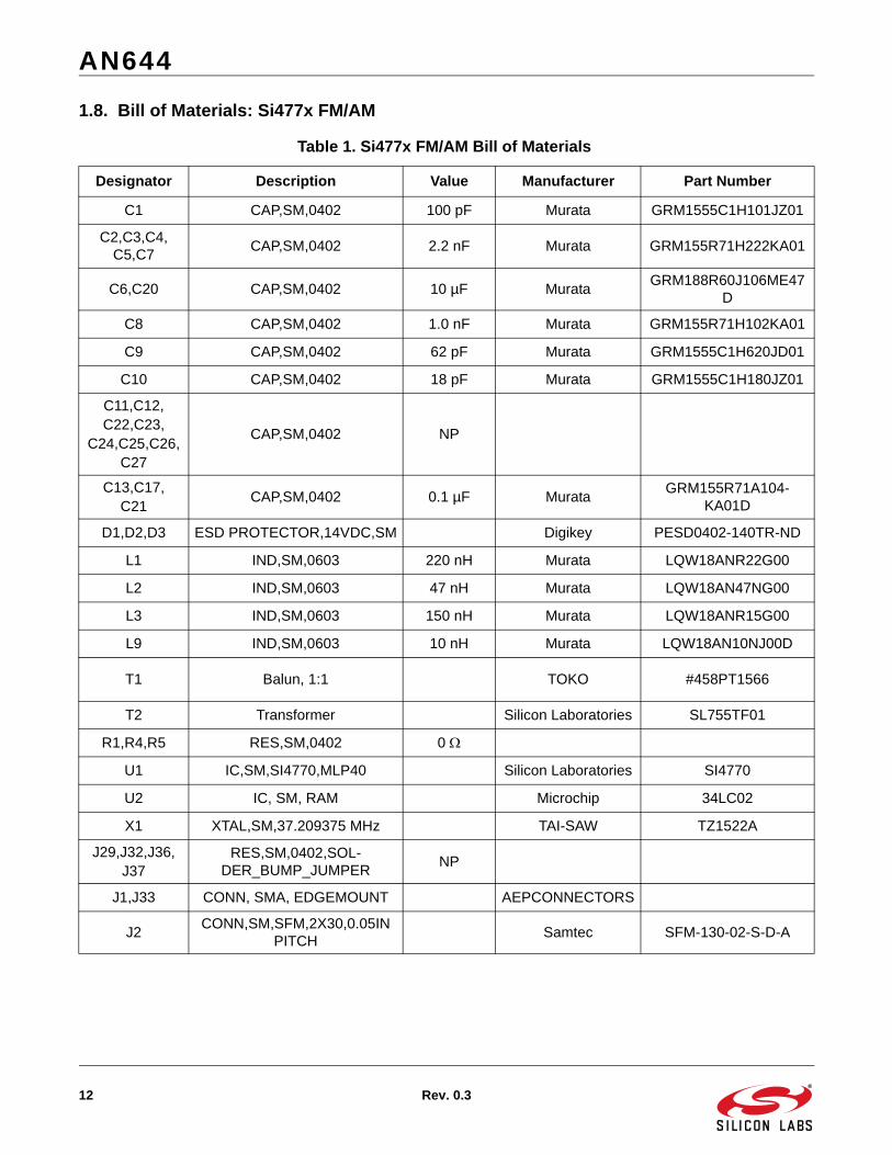
1.8. Bill of Materials: Si477x FM/AM
Table 1. Si477x FM/AM Bill of Materials
Designator Description Value Manufacturer Part Number
C1 CAP,SM,0402 100 pF Murata GRM1555C1H101JZ01
C2,C3,C4,C5,C7
CAP,SM,0402 2.2 nF Murata GRM155R71H222KA01
C6,C20 CAP,SM,0402 10 µF MurataGRM188R60J106ME47
D
C8 CAP,SM,0402 1.0 nF Murata GRM155R71H102KA01
C9 CAP,SM,0402 62 pF Murata GRM1555C1H620JD01
C10 CAP,SM,0402 18 pF Murata GRM1555C1H180JZ01
C11,C12,C22,C23,
C24,C25,C26,C27
CAP,SM,0402 NP
C13,C17,C21
CAP,SM,0402 0.1 µF MurataGRM155R71A104-
KA01D
D1,D2,D3 ESD PROTECTOR,14VDC,SM Digikey PESD0402-140TR-ND
L1 IND,SM,0603 220 nH Murata LQW18ANR22G00
L2 IND,SM,0603 47 nH Murata LQW18AN47NG00
L3 IND,SM,0603 150 nH Murata LQW18ANR15G00
L9 IND,SM,0603 10 nH Murata LQW18AN10NJ00D
T1 Balun, 1:1 TOKO #458PT1566
T2 Transformer Silicon Laboratories SL755TF01
R1,R4,R5 RES,SM,0402 0
U1 IC,SM,SI4770,MLP40 Silicon Laboratories SI4770
U2 IC, SM, RAM Microchip 34LC02
X1 XTAL,SM,37.209375 MHz TAI-SAW TZ1522A
J29,J32,J36,J37
RES,SM,0402,SOL-DER_BUMP_JUMPER
NP
J1,J33 CONN, SMA, EDGEMOUNT AEPCONNECTORS
J2CONN,SM,SFM,2X30,0.05IN
PITCH Samtec SFM-130-02-S-D-A

AN644
Rev. 0.3 13
JP1CONN,TH,HEADER,.100
PITCH,1X2Samtec HTSW-101-07-G-D
J3,J4,J5,J6,J7,J8,J9,J10,J11,J12,J13,J14,J15,J16,J17,J18,J19,J20,J21,J22,J23,J24,J25,J26,J27,J28,J30,
J31,J35
RES,SM,0402,SOL-DER_BUMP_JUMPER
0
Table 1. Si477x FM/AM Bill of Materials (Continued)
Designator Description Value Manufacturer Part Number

AN644
14 Rev. 0.3
DOCUMENT CHANGE LIST
Revision 0.1 to Revision 0.2 Updated "1.3.1. FM Front-End" on page 3.
Revision 0.2 to Revision 0.3 Updated Table 1 on page 12.
Updated T1 designator part number.

DisclaimerSilicon Laboratories intends to provide customers with the latest, accurate, and in-depth documentation of all peripherals and modules available for system and software implementers using or intending to use the Silicon Laboratories products. Characterization data, available modules and peripherals, memory sizes and memory addresses refer to each specific device, and "Typical" parameters provided can and do vary in different applications. Application examples described herein are for illustrative purposes only. Silicon Laboratories reserves the right to make changes without further notice and limitation to product information, specifications, and descriptions herein, and does not give warranties as to the accuracy or completeness of the included information. Silicon Laboratories shall have no liability for the consequences of use of the information supplied herein. This document does not imply or express copyright licenses granted hereunder to design or fabricate any integrated circuits. The products must not be used within any Life Support System without the specific written consent of Silicon Laboratories. A "Life Support System" is any product or system intended to support or sustain life and/or health, which, if it fails, can be reasonably expected to result in significant personal injury or death. Silicon Laboratories products are generally not intended for military applications. Silicon Laboratories products shall under no circumstances be used in weapons of mass destruction including (but not limited to) nuclear, biological or chemical weapons, or missiles capable of delivering such weapons.
Trademark InformationSilicon Laboratories Inc., Silicon Laboratories, Silicon Labs, SiLabs and the Silicon Labs logo, CMEMS®, EFM, EFM32, EFR, Energy Micro, Energy Micro logo and combinations thereof, "the world’s most energy friendly microcontrollers", Ember®, EZLink®, EZMac®, EZRadio®, EZRadioPRO®, DSPLL®, ISOmodem ®, Precision32®, ProSLIC®, SiPHY®, USBXpress® and others are trademarks or registered trademarks of Silicon Laboratories Inc. ARM, CORTEX, Cortex-M3 and THUMB are trademarks or registered trademarks of ARM Holdings. Keil is a registered trademark of ARM Limited. All other products or brand names mentioned herein are trademarks of their respective holders.
http://www.silabs.com
Silicon Laboratories Inc.400 West Cesar ChavezAustin, TX 78701USA
Smart.Connected.Energy-Friendly
Productswww.silabs.com/products
Qualitywww.silabs.com/quality
Support and Communitycommunity.silabs.com