si306xrev0 9 - Digi-Key Sheets/Silicon Laboratories PDFs... · 1 2 3 4 5 6 7 8 9 10 11 12 13 16 15...
62
Rev. 0.9 1/05 Copyright © 2005 by Silicon Laboratories Si306x Si306x G LOBAL L INE -S IDE DAA FOR E MBEDDED S YSTEM -S IDE M ODULE Features Complete DAA includes the following: Applications Description The Si306x is an integrated direct access arrangement (DAA) with a programmable line interface to meet global telephone line interface requirements. Available in a 16-pin small outline package, it eliminates the need for an analog front end (AFE), an isolation transformer, relays, opto-isolators, and a 2- to 4-wire hybrid. The Si306x dramatically reduces the number of discrete components and cost required to achieve compliance with global regulatory requirements. The Si306x interfaces directly to a Silicon Laboratories integrated DAA system-side module. Functional Block Diagram 80 dB dynamic range TX/RX paths to support up to V.92 modem speeds Programmable line interface z AC termination z DC termination z Ring detect threshold z Ringer impedance Integrated codec and 2- to 4-wire analog hybrid Integrated ring detector Pulse dialing support Billing tone detection Overload detection > 5000 V isolation Proprietary isolation interface to integrated DAA module Line voltage monitor Loop current monitor Caller ID support Low-profile SOIC available in lead- free/ROHS-compliant packages V.92 soft modems PDAs Set-top boxes Fax machines POS terminals Multi-function Printers Isolation Interface Hybrid and dc Termination Ring Detect Off-Hook Si306x QE2 QE QB RNG2 RNG1 DCT3 DCT2 VREG2 VREG DCT SC IB RX Silicon Laboratories Embedded System-side DAA Module US Patent # 5,870,046 US Patent # 6,061,009 Other Patents Pending Ordering Information See page 59. Pin Assignments Si306x 1 2 3 4 5 6 7 8 9 10 11 12 13 16 15 14 QE DCT RX IB C1B C2B VREG RNG1 DCT2 IGND DCT3 QB QE2 SC VREG2 RNG2
Transcript of si306xrev0 9 - Digi-Key Sheets/Silicon Laboratories PDFs... · 1 2 3 4 5 6 7 8 9 10 11 12 13 16 15...

Rev. 0.9 1/05 Copyright © 2005 by Silicon Laboratories Si306x
Si306x
GLOBAL LINE-SIDE DAA FOR EMBEDDED SYSTEM-SIDE MODULE
Features
Complete DAA includes the following:
Applications
Description
The Si306x is an integrated direct access arrangement (DAA) with aprogrammable line interface to meet global telephone line interfacerequirements. Available in a 16-pin small outline package, it eliminatesthe need for an analog front end (AFE), an isolation transformer, relays,opto-isolators, and a 2- to 4-wire hybrid. The Si306x dramatically reducesthe number of discrete components and cost required to achievecompliance with global regulatory requirements. The Si306x interfacesdirectly to a Silicon Laboratories integrated DAA system-side module.
Functional Block Diagram
80 dB dynamic range TX/RX paths to support up to V.92 modem speedsProgrammable line interface
AC termination DC termination Ring detect threshold Ringer impedance
Integrated codec and 2- to 4-wire analog hybridIntegrated ring detector
Pulse dialing supportBilling tone detectionOverload detection> 5000 V isolationProprietary isolation interface to integrated DAA moduleLine voltage monitorLoop current monitorCaller ID supportLow-profile SOIC available in lead-free/ROHS-compliant packages
V.92 soft modemsPDAs
Set-top boxesFax machines
POS terminalsMulti-function Printers
IsolationInterface
Hybrid anddc
Termination
Ring DetectOff-Hook
Si306x
QE2QEQBRNG2RNG1
DCT3DCT2VREG2VREGDCT
SCIB
RX
SiliconLaboratoriesEmbedded
System-sideDAA Module
US Patent # 5,870,046US Patent # 6,061,009Other Patents Pending
Ordering InformationSee page 59.
Pin Assignments
Si306x
1
2
3
4
5
6
7
8 9
1011
1213
16
1514
QEDCT
RXIB
C1BC2B
VREGRNG1
DCT2IGNDDCT3QBQE2SCVREG2RNG2

Si306x
2 Rev. 0.9
1. Si306x Selection Guide
System-Side Requirement
Part Number Description Region AC Terminations
Line Voltage
Monitoring
For use with integrated
system-side module only
Si3060-X-FS FCC Line-side FCC 1 No
Si3061-X-FS Global Line-side Global 4 No
Si3062-X-FS Enhanced FCC Line-side
FCC 1 Yes
Si3063-X-FS Enhanced Global Line-side
Global 4 Yes
Si3065-X-FS EnhancedFCC/TBR21
Line-side
FCC/TBR21
2 Yes

Rev. 0.9 3
Si306xTABLE OF CONTENTS
Section Page1. Si306x Selection Guide . . . . . . . . . . . . . . . . . . . . . . . . . . . . . . . . . . . . . . . . . . . . . . . . . . . .22. Electrical Specifications . . . . . . . . . . . . . . . . . . . . . . . . . . . . . . . . . . . . . . . . . . . . . . . . . . .43. Typical Application Schematic . . . . . . . . . . . . . . . . . . . . . . . . . . . . . . . . . . . . . . . . . . . . . .94. Bill of Materials . . . . . . . . . . . . . . . . . . . . . . . . . . . . . . . . . . . . . . . . . . . . . . . . . . . . . . . . . .105. AOUT PWM Output . . . . . . . . . . . . . . . . . . . . . . . . . . . . . . . . . . . . . . . . . . . . . . . . . . . . . . .116. Functional Description . . . . . . . . . . . . . . . . . . . . . . . . . . . . . . . . . . . . . . . . . . . . . . . . . . .12
6.1. Line-Side Device Support . . . . . . . . . . . . . . . . . . . . . . . . . . . . . . . . . . . . . . . . . . . . .126.2. Power Supplies . . . . . . . . . . . . . . . . . . . . . . . . . . . . . . . . . . . . . . . . . . . . . . . . . . . . .166.3. Initialization . . . . . . . . . . . . . . . . . . . . . . . . . . . . . . . . . . . . . . . . . . . . . . . . . . . . . . . .166.4. Isolation Barrier . . . . . . . . . . . . . . . . . . . . . . . . . . . . . . . . . . . . . . . . . . . . . . . . . . . . .166.5. Power Management . . . . . . . . . . . . . . . . . . . . . . . . . . . . . . . . . . . . . . . . . . . . . . . . .166.6. Calibration . . . . . . . . . . . . . . . . . . . . . . . . . . . . . . . . . . . . . . . . . . . . . . . . . . . . . . . . .176.7. In-Circuit Testing . . . . . . . . . . . . . . . . . . . . . . . . . . . . . . . . . . . . . . . . . . . . . . . . . . . .176.8. Exception Handling . . . . . . . . . . . . . . . . . . . . . . . . . . . . . . . . . . . . . . . . . . . . . . . . . .186.9. Revision Identification . . . . . . . . . . . . . . . . . . . . . . . . . . . . . . . . . . . . . . . . . . . . . . . .186.10. Parallel Handset Detection . . . . . . . . . . . . . . . . . . . . . . . . . . . . . . . . . . . . . . . . . . .186.11. Line Voltage/Loop Current Sensing . . . . . . . . . . . . . . . . . . . . . . . . . . . . . . . . . . . .186.12. Off-Hook . . . . . . . . . . . . . . . . . . . . . . . . . . . . . . . . . . . . . . . . . . . . . . . . . . . . . . . . .206.13. Interrupts . . . . . . . . . . . . . . . . . . . . . . . . . . . . . . . . . . . . . . . . . . . . . . . . . . . . . . . . .206.14. DC Termination . . . . . . . . . . . . . . . . . . . . . . . . . . . . . . . . . . . . . . . . . . . . . . . . . . . .206.15. AC Termination . . . . . . . . . . . . . . . . . . . . . . . . . . . . . . . . . . . . . . . . . . . . . . . . . . . .216.16. Transhybrid Balance . . . . . . . . . . . . . . . . . . . . . . . . . . . . . . . . . . . . . . . . . . . . . . . .226.17. Ring Detection . . . . . . . . . . . . . . . . . . . . . . . . . . . . . . . . . . . . . . . . . . . . . . . . . . . . .226.18. Ring Validation . . . . . . . . . . . . . . . . . . . . . . . . . . . . . . . . . . . . . . . . . . . . . . . . . . . .226.19. Ringer Impedance and Threshold . . . . . . . . . . . . . . . . . . . . . . . . . . . . . . . . . . . . . .236.20. Pulse Dialing and Spark Quenching . . . . . . . . . . . . . . . . . . . . . . . . . . . . . . . . . . . .236.21. Billing Tone Detection and Receive Overload . . . . . . . . . . . . . . . . . . . . . . . . . . . . .236.22. Billing Tone Filter (Optional) . . . . . . . . . . . . . . . . . . . . . . . . . . . . . . . . . . . . . . . . . .246.23. On-Hook Line Monitor . . . . . . . . . . . . . . . . . . . . . . . . . . . . . . . . . . . . . . . . . . . . . . .246.24. Caller ID . . . . . . . . . . . . . . . . . . . . . . . . . . . . . . . . . . . . . . . . . . . . . . . . . . . . . . . . .256.25. Overload Detection . . . . . . . . . . . . . . . . . . . . . . . . . . . . . . . . . . . . . . . . . . . . . . . . .266.26. Gain Control . . . . . . . . . . . . . . . . . . . . . . . . . . . . . . . . . . . . . . . . . . . . . . . . . . . . . .266.27. Clock Generation . . . . . . . . . . . . . . . . . . . . . . . . . . . . . . . . . . . . . . . . . . . . . . . . . .26
7. Control Registers . . . . . . . . . . . . . . . . . . . . . . . . . . . . . . . . . . . . . . . . . . . . . . . . . . . . . . . .28Appendix—UL1950 3rd Edition . . . . . . . . . . . . . . . . . . . . . . . . . . . . . . . . . . . . . . . . . . . . . . .568. Pin Descriptions: Si306x . . . . . . . . . . . . . . . . . . . . . . . . . . . . . . . . . . . . . . . . . . . . . . . . . .579. Ordering Guide . . . . . . . . . . . . . . . . . . . . . . . . . . . . . . . . . . . . . . . . . . . . . . . . . . . . . . . . . .5910. Product Identification . . . . . . . . . . . . . . . . . . . . . . . . . . . . . . . . . . . . . . . . . . . . . . . . . . .5911. Package Outline: 16-Pin SOIC . . . . . . . . . . . . . . . . . . . . . . . . . . . . . . . . . . . . . . . . . . . . .60Document Change List . . . . . . . . . . . . . . . . . . . . . . . . . . . . . . . . . . . . . . . . . . . . . . . . . . . . .61Contact Information . . . . . . . . . . . . . . . . . . . . . . . . . . . . . . . . . . . . . . . . . . . . . . . . . . . . . . . .62

Si306x
4 Rev. 0.9
2. Electrical Specifications
Table 1. Recommended Operating Conditions
Parameter1 Symbol Test Condition Min2 Typ Max2 Unit
Ambient Temperature TA F/K-Grade 0 25 70 °C
Notes:1. The Si306x specifications are guaranteed when the typical application circuit (including component tolerance) and any
system-side module and any Si306x are used. See "3. Typical Application Schematic" on page 9.2. All minimum and maximum specifications are guaranteed and apply across the recommended operating conditions.
Typical values apply at nominal supply voltages and an operating temperature of 25 °C unless otherwise stated.

Si306x
Rev. 0.9 5
Figure 1. Test Circuit for Loop Characteristics
Table 2. Loop Characteristics (VD = 3.0 to 3.6 V, TA = 0 to 70 °C for F/K-Grade, see Figure 1)
Parameter Symbol Test Condition Min Typ Max UnitDC Termination Voltage VTR IL = 20 mA, MINI = 11,
ILIM = 0, DCV = 00, DCR = 0— — 6.0 V
DC Termination Voltage VTR IL = 120 mA, MINI = 11, ILIM = 0, DCV = 00, DCR = 0
9 — — V
DC Termination Voltage VTR IL = 20 mA, MINI = 00, ILIM = 0, DCV = 11, DCR = 0
— — 7.5 V
DC Termination Voltage VTR IL = 120 mA, MINI = 00, ILIM = 0, DCV = 11, DCR = 0
9 — — V
DC Termination Voltage VTR IL = 20 mA, MINI = 00,ILIM = 1, DCV = 11, DCR = 0
— — 7.5 V
DC Termination Voltage VTR IL = 60 mA, MINI = 00,ILIM = 1, DCV = 11, DCR = 0
40 — — V
On Hook Leakage Current ILK VTR = –48 V — — 3 µAOperating Loop Current ILP MINI = 00, ILIM = 0 10 — 120 mAOperating Loop Current ILP MINI = 00, ILIM = 1 10 — 60 mADC Ring Current — 1.5 3 µA
Ring Detect Voltage* VRD RT = 0 13.5 15 16.5 Vrms
Ring Detect Voltage* VRD RT = 1 19.35 21.5 23.65 Vrms
Ring Frequency FR 15 — 68 Hz
Ringer Equivalence Number REN — — 0.2
*Note: The ring signal is guaranteed to not be detected below the minimum. The ring signal is guaranteed to be detected above the maximum.
TIP
RING
+
–
VTR
600 Ω
10 µF
ILDAALine-sideDevice

Si306x
6 Rev. 0.9
Table 3. DC Characteristics, VD = 3.3 V(VD = 3.0 to 3.6 V, TA = 0 to 70 °C)
Parameter Symbol Test Condition Min Typ Max Unit
Input Leakage Current IL –10 — 10 µA
Power Supply Current, Analog* ID VA pin — 9 12 mA
*Note: This current is required from the integrated system-side interface to communicate with the Si306x through the proprietary isolation interface.

Si306x
Rev. 0.9 7
Table 4. AC Characteristics (VD = 3.0 to 3.6 V, TA = 0 to 70 °C for F/K-Grade, see "3. Typical Application Schematic" on page 9)
Parameter Symbol Test Condition Min Typ Max Unit
Sample Rate Fs 7.2 — 161 kHz
Transmit Frequency Response Low –3 dBFS Corner — 0 — Hz
Receive Frequency Response Low –3 dBFS Corner, FILT = 0
— 5 — Hz
Receive Frequency Response Low –3 dBFS Corner, FILT = 1
— 200 — Hz
Transmit Full Scale Level2 VFS FULL = 0 (0 dBM) — 1.1 — VPEAK
Receive Full Scale Level2,3 VFS FULL = 0 (0 dBM) 1.1 VPEAK
Dynamic Range4,5 DR ILIM = 0, DCV = 11, DCR = 0, IL = 120 mA, MINI = 00
— 80 — dB
Dynamic Range4,5 DR ILIM = 0, DCV = 00, DCR = 0, IL = 20 mA, MINI = 11
— 80 — dB
Dynamic Range4,5 DR ILIM = 1, DCV = 11, DCR = 0, IL = 60 mA, MINI = 00
— 80 — dB
Transmit Total Harmonic Distortion6 THD ILIM = 0, DCV = 11, DCR = 0, IL = 100 mA, MINI = 00
— –72 — dB
Transmit Total Harmonic Distortion6 THD ILIM = 0, DCV = 00, DCR = 0, IL = 20 mA, MINI = 11
— –78 — dB
Receive Total Harmonic Distortion6 THD ILIM = 0, DCV = 00, DCR = 0, IL = 20 mA, MINI = 11
— –78 — dB
Receive Total Harmonic Distortion6 THD ILIM = 1, DCV = 11, DCR = 0, IL = 50 mA, MINI = 00
— –78 — dB
Dynamic Range (caller ID mode)7 DRCID VIN = 1 kHz, –13 dBFS — 50 — dB
Caller ID Full Scale Level8 VCID — 1.6 — VPEAK
AOUT Low Level Current — — 10 mA
AOUT High Level Current — — 10 mA
Notes:1. The 32.768 MHz system-side module supports sample rates up to 16 kHz. The 32.4 MHz system-side module supports
sample rates up to a maximum of 10.286 MHz.2. Measured at TIP and RING with 600 Ω termination at 1 kHz, as shown in Figure 1.3. Receive full scale level produces –0.9 dBFS at SDO.4. DR = 20 x log (RMS VFS/RMS VIN) + 20 x log (RMS VIN/RMS noise). VFS is the 0 dBm full-scale level. RMS noise
measurement excludes harmonics. VFS is the 0 dBm full-scale level.5. Measurement is 300 to 3400 Hz. Applies to both transmit and receive paths. Vin = 1 kHz, –3 dBFS, Fs = 10300 Hz.6. THD = 20 x log (RMS distortion/RMS signal). Vin = 1 kHz, –3 dBFS, Fs = 10300 Hz.7. DRCID = 20 x log (RMS VCID/RMS VIN) + 20 x log (RMS VIN/RMS noise). VCID is the 1.5 V full-scale level for the typical
application circuit in Figure 2.8. With the enhanced CID circuit (refer to "4. Bill of Materials" on page 10), VCID = 1.5 VPEAK and DRCID = 62 dB.

Si306x
8 Rev. 0.9
Table 5. Absolute Maximum Ratings
Parameter Symbol Value Unit
Operating Temperature Range TA –40 to 100 °C
Storage Temperature Range TSTG –65 to 150 °C
Note: Permanent device damage can occur if the above Absolute Maximum Ratings are exceeded. Restrict functional operation to the conditions as specified in the operational sections of this data sheet. Exposure to absolute maximum rating conditions for extended periods might affect device reliability.

Si306x
Rev. 0.9 9
3. Typical Application Schematic
Q3
Q1
Q4
RV
1
C3
R5
R6
R30
R32
R31
R33
C30
C31
R12
R16
R15
OptionalCIDEnhancement
R13
FB
2
+
C4
FB
1
Z1
C5
C7
R10
R7R
8
R2
R9
R1
C1
C2
Q5
R3
Q2
J1
RJ-
11S
MD
1 2 3 4 5 6
-+D
1
R4
No
Gro
und
Pla
neIn
DA
AS
ectio
n
R11
C10
U1
AO
UT
C1A
C2A
Host
Processer
Integrated
Digital
Interface
C6
C8
C9
U2
Si3
06x
QE
1
DC
T2
RX
3
IB4
C1B
5
C2B
6
VR
EG
7
RN
G1
8
DC
T216
IGN
D15
DC
T314
QB
13
QE
212
SC
11
VR
EG
210
RN
G2
9
Figu
re2.
Typi
cal A
pplic
atio
n C
ircui
t for
the
Si30
6x L
ine-
side
dev
ice
(Ref
er to
“A
N67
: Si3
050/
52/5
4/56
Lay
out G
uide
lines
” fo
r rec
omm
ende
d la
yout
gui
delin
es)

Si306x
10 Rev. 0.9
4. Bill of Materials
Component(s) Value Supplier(s)C1, C21 33 pF, Y2, X7R, ±20% Panasonic, Murata, Vishay
C3 10 nF, 250 V, X7R, ±20% Venkel, SMEC
C4 1.0 µF, 50 V, Elec/Tant, ±20% Panasonic
C5, C6 0.1 µF, 16 V, X7R, ±20% Venkel, SMEC
C7 2.7 nF, 50 V, X7R, ±20% Venkel, SMEC
C8, C9 680 pF, Y2, X7R, ±10% Panasonic, Murata, Vishay
C10 0.01 µF, 16 V, X7R, ±20% Venkel, SMEC
C30, C315 Not installed, 120 pF, 250 V, X7R, ±10% Venkel, SMEC
D1, D22 Dual Diode, 225 mA, 300 V, CMPD2004 Central Semiconductor
FB1, FB2 Ferrite Bead, BLM18AG601SN1 Murata
Q1, Q3 NPN, 300 V, MMBTA42 Central Semiconductor, OnSemi, Fairchild
Q2 PNP, 300 V, MMBTA92 Central Semiconductor, OnSemi, Fairchild
Q4, Q5 NPN, 60 V, 330 mW, MMBTA06 Central Semiconductor, OnSemi, Fairchild
RV1 Sidactor, 275 V, 100 A Teccor, ST Micro, Diodes Inc., Shindengen
R1 1.07 kΩ, 1/2 W, 1% Venkel, SMEC, Panasonic
R2 150 Ω, 1/16 W, 5% Venkel, SMEC, Panasonic
R3 3.65 kΩ, 1/2 W, 1% Venkel, SMEC, Panasonic
R4 2.49 kΩ, 1/2 W, 1% Venkel, SMEC, Panasonic
R5, R6 100 kΩ, 1/16 W, 5% Venkel, SMEC, Panasonic
R7, R8 20 MΩ, 1/16 W, 5% Venkel, SMEC, Panasonic
R9 1 MΩ, 1/16 W, 1% Venkel, SMEC, Panasonic
R10 536 Ω, 1/4 W, 1% Venkel, SMEC, Panasonic
R11 73.2 Ω, 1/2 W, 1% Venkel, SMEC, Panasonic
R12, R133 56.2 Ω, 1/16 W, 5% Venkel, SMEC, Panasonic
R15, R164 0 Ω, 1/16 W, 5% Venkel, SMEC, Panasonic
R30, R325 Not installed, 15 MΩ, 1/8 W, 5% Venkel, SMEC, Panasonic
R31, R335 Not installed, 5.1 MΩ, 1/8 W, 5% Venkel, SMEC, Panasonic
U1 SiLabs Integrated System-Side Interface Silicon Labs
U2 Si306x line-side device Silicon Labs
Z1 Zener Diode, 43 V, 1/2 W General Semi, Diodes Inc.,OnSemiNotes:
1. X2/Y3 or Y2 rated capacitors can be used to comply with Nordic supplemental insulation requirements. Additional vendors for these safety-rated capacitors include Novacap, Syfer, and Kyocera.
2. Several diode bridge configurations are acceptable. Parts, such as a single DF-04S or four 1N4004 diodes, may be used.
3. 56 Ω, 1/16 W, 1% resistors may be substituted for R12-R13 (0 Ω) to decrease emissions.4. Murata BLM18AG601SN1 may be substituted for R15-R16 (0 Ω) to decrease emissions.5. C30-C31 and R30-R33 can be substituted for R7-R8 to implement the enhanced caller ID circuit.

Si306x
Rev. 0.9 11
5. AOUT PWM OutputFigure 3 illustrates an optional circuit to support the pulse width modulation (PWM) output capability of the Si306xfor call progress monitoring purposes. To enable this mode, the INTE bit (Register 2) should be set to 0, the PWMEbit (Register 1) set to 1, and the PWMM bits (Register 1) set to 00.
Figure 3. AOUT PWM Circuit for Call Progress
Registers 20 and 21 allow the receive and transmit paths to be attenuated linearly. When these registers are set toall 0s, the receive and transmit paths are muted. These registers affect the call progress output only and do notaffect transmit and receive operations on the telephone line.The PWMM[1:0] bits (Register 1, bits 5:4) select one of the three different PWM output modes for the AOUT signal,including a delta-sigma data stream, a 32 kHz return to zero PWM output, and balanced 32 kHz PWM output.
Table 6. Component Values—AOUT PWM
Component Value Supplier
LS1 Speaker BRT1209PF-06 Intervox
Q6 NPN KSP13 Fairchild
C41 0.1 µF, 16 V, X7R, ±20% Venkel, SMEC
R41 150 Ω, 1/16 W, ±5% Venkel, SMEC, Panasonic
+5 VA
LS1
Q6 NPNR41
C41
AOUT

Si306x
12 Rev. 0.9
6. Functional DescriptionThe Si306x is an integrated direct access arrangement(DAA) that provides a programmable line interface tomeet global telephone line interface requirements. TheSi306x implements Silicon Laboratories’ proprietarycapacitive isolation technology and offers the highestlevel of integration by replacing an analog front end(AFE), an isolation transformer, relays, opto-isolators,and a 2- to 4-wire hybrid with a single 16-pin packages(SOIC). The Si306x DAA can be programmed with software tomeet global requirements and is compliant with FCC,TBR21, JATE, and other country-specific PTTspecifications as shown in Table 9 on page 20. Inaddition, the Si306x meets the most stringent worldwiderequirements for out-of-band energy, emissions,immunity, high-voltage surges, and safety, includingFCC Part 15 and 68, EN55022, EN55024, and manyother standards.
6.1. Line-Side Device SupportSilicon Labs offers five different line-side devices in theSi306x family that can be used with the SiLabsintegrated system-side module. All five Si306x line-sidedevices are capable of supporting modem speeds ofV.22 through V.92.
The Si306x line-side device family includes solutions to meet regional PTT specifications or global devices to meet worldwide DAA requirements. Si3060 and Si3062: Single ac termination to meet FCC
PTT specifications. Si3065: Two ac termination settings to meet FCC and
TBR21 PTT specifications. Si3061 and Si3063: Four ac termination settings to meet
global PTT specifications.The Si3062, Si3063, and Si3065 enhanced line-side devices additionally provide line voltage monitoring and finer resolution loop current monitoring capabilities. Line voltage monitoring in on-hook and off-hook modes
enables non-intrusive line-in-use/parallel handset detection. Polarity reversal interrupt simplifies support of Type II
Caller ID. Line current/voltage interrupts improve line monitoring
capability.

Si306x
Rev. 0.9 13
Table 7. Country Specific Register Settings
Register 16 31 16 16 26 26 26 163
Country OHS OHS2 RZ RT ILIM DCV[1:0] MINI[1:0] ACT ACT2
Argentina 0 0 0 0 0 11 00 0 0
Australia4 1 0 0 0 0 01 01 0 1
Austria 0 1 0 0 1 11 00 0 1
Bahrain 0 1 0 0 1 11 00 0 1
Belgium 0 1 0 0 1 11 00 0 1
Brazil 0 0 0 0 0 11 00 0 0
Bulgaria 0 1 0 0 1 11 00 0 1
Canada 0 0 0 0 0 11 00 0 0
Chile 0 0 0 0 0 11 00 0 0
China 0 0 0 0 0 11 00 0 0
Colombia 0 0 0 0 0 11 00 0 0
Croatia 0 1 0 0 1 11 00 0 1
Cyprus 0 1 0 0 1 11 00 0 1
Czech Republic 0 1 0 0 1 11 00 0 1
Denmark 0 1 0 0 1 11 00 0 1
Ecuador 0 0 0 0 0 11 00 0 0
Egypt 0 1 0 0 1 11 00 0 1
El Salvador 0 0 0 0 0 11 00 0 0
Finland 0 1 0 0 1 11 00 0 1
France 0 1 0 0 1 11 00 0 1
Germany 0 1 0 0 1 11 00 0 1
Greece 0 1 0 0 1 11 00 0 1
Guam 0 0 0 0 0 11 00 0 0
Hong Kong 0 0 0 0 0 11 00 0 0
Hungary 0 1 0 0 1 11 00 0 1
Iceland 0 1 0 0 1 11 00 0 1
India 0 0 0 0 0 11 00 0 0
Note:1. TBR21 includes the following countries: Austria, Belgium, Denmark, Finland, France, Germany, Greece,
Iceland, Ireland, Italy, Luxembourg, Netherlands, Norway, Portugal, Spain, Sweden, Switzerland, and the United Kingdom.
2. Supported for loop current ≥ 20 mA.3. Available with Si3061, Si3063, and Si3065 line-sides only. See "6.15. AC Termination" on page 21.4. See "6.14. DC Termination" on page 20 for DCV and MINI settings.

Si306x
14 Rev. 0.9
Indonesia 0 0 0 0 0 11 00 0 0
Ireland 0 1 0 0 1 11 00 0 1
Israel 0 1 0 0 1 11 00 0 1
Italy 0 1 0 0 1 11 00 0 1
Japan 0 0 0 0 0 01 01 0 0
Jordan 0 0 0 0 0 01 01 0 0
Kazakhstan 0 0 0 0 0 11 00 0 0
Kuwait 0 0 0 0 0 11 00 0 0
Latvia 0 1 0 0 1 11 00 0 1
Lebanon 0 1 0 0 1 11 00 0 1
Luxembourg 0 1 0 0 1 11 00 0 1
Macao 0 0 0 0 0 11 00 0 0
Malaysia2 0 0 0 0 0 01 01 0 0
Malta 0 1 0 0 1 11 00 0 1
Mexico 0 0 0 0 0 11 00 0 0
Morocco 0 1 0 0 1 11 00 0 1
Netherlands 0 1 0 0 1 11 00 0 1
New Zealand 0 0 0 0 0 11 00 1 1
Nigeria 0 1 0 0 1 11 00 0 1
Norway 0 1 0 0 1 11 00 0 1
Oman 0 0 0 0 0 01 01 0 0
Pakistan 0 0 0 0 0 01 01 0 0
Peru 0 0 0 0 0 11 00 0 0
Philippines 0 0 0 0 0 01 01 0 0
Poland 0 1 0 0 1 11 00 0 1
Portugal 0 1 0 0 1 11 00 0 1
Romania 0 1 0 0 1 11 00 0 1
Russia 0 0 0 0 0 11 00 0 0
Table 7. Country Specific Register Settings (Continued)
Register 16 31 16 16 26 26 26 163
Country OHS OHS2 RZ RT ILIM DCV[1:0] MINI[1:0] ACT ACT2
Note:1. TBR21 includes the following countries: Austria, Belgium, Denmark, Finland, France, Germany, Greece,
Iceland, Ireland, Italy, Luxembourg, Netherlands, Norway, Portugal, Spain, Sweden, Switzerland, and the United Kingdom.
2. Supported for loop current ≥ 20 mA.3. Available with Si3061, Si3063, and Si3065 line-sides only. See "6.15. AC Termination" on page 21.4. See "6.14. DC Termination" on page 20 for DCV and MINI settings.

Si306x
Rev. 0.9 15
Saudi Arabia 0 0 0 0 0 11 00 0 0
Singapore 0 0 0 0 0 11 00 0 0
Slovakia 0 1 0 0 1 11 00 0 1
Slovenia 0 1 0 0 1 11 00 0 1
South Africa 0 0 1 0 0 11 00 1 0
South Korea 0 0 1 0 0 11 00 0 0
Spain 0 1 0 0 1 11 00 0 1
Sweden 0 1 0 0 1 11 00 0 1
Switzerland 0 1 0 0 1 11 00 0 1
Taiwan 0 0 0 0 0 11 00 0 0
TBR211 0 1 0 0 1 11 00 0 1
Thailand 0 0 0 0 0 01 01 0 0
UAE 0 0 0 0 0 11 00 0 0
United Kingdom 0 1 0 0 1 11 00 0 1
USA 0 0 0 0 0 11 00 0 0
Yemen 0 0 0 0 0 11 00 0 0
Table 7. Country Specific Register Settings (Continued)
Register 16 31 16 16 26 26 26 163
Country OHS OHS2 RZ RT ILIM DCV[1:0] MINI[1:0] ACT ACT2
Note:1. TBR21 includes the following countries: Austria, Belgium, Denmark, Finland, France, Germany, Greece,
Iceland, Ireland, Italy, Luxembourg, Netherlands, Norway, Portugal, Spain, Sweden, Switzerland, and the United Kingdom.
2. Supported for loop current ≥ 20 mA.3. Available with Si3061, Si3063, and Si3065 line-sides only. See "6.15. AC Termination" on page 21.4. See "6.14. DC Termination" on page 20 for DCV and MINI settings.

Si306x
16 Rev. 0.9
6.2. Power SuppliesThe Si306x line-side device derives its power from twosources: The system-side module and the telephoneline. The integrated system-side module supplies powerover the patented capacitive isolation link between thetwo devices, allowing the line-side device tocommunicate with the system-side module while on-hook and perform other on-hook functions such as linevoltage monitoring. When off-hook, the line-side devicealso derives power from the line current supplied fromthe telephone line. This feature is exclusive to DAAsfrom Silicon Laboratories and allows the most costeffective implementation for a DAA while stillmaintaining robust performance over all line conditions.
6.3. InitializationWhen the integrated system-side module is poweredup, assert the RESET pin. When the RESET pin isdeasserted, the registers have default values. This resetcondition guarantees the line-side device is powereddown without the possibility of loading the line (i.e., off-hook). An example initialization procedure is outlined inthe following list:1. Program the desired sample rate with the Sample
Rate Control Register (Register 7).2. Wait until the line-side PLL is locked. This time is
normally between 100 µs and 1 ms from the application of MCLK.
3. Write a 00H into the DAA Control Register (Register 6) to power up the line-side device.
4. Set the required line interface parameters MINI[1:0], ILIM, DCR, ACT and ACT2, OHS, RT, RZ, ATX[2:0] and ARX[2:0] as defined by “Country Specific Register Settings” shown in Table 7.
When this procedure is complete, the Si306x is readyfor ring detection and off-hook.
6.4. Isolation BarrierThe Si306x achieves an isolation barrier through low-cost, high-voltage capacitors in conjunction with SiliconLaboratories’ proprietary signal processing techniques.These techniques eliminate signal degradation fromcapacitor mismatches, common mode interference, ornoise coupling. As shown in "3. Typical ApplicationSchematic" on page 9, the C1, C2, C8, and C9capacitors isolate the integrated system-side modulefrom the line-side device. Transmit, receive, control, ringdetect, and caller ID data are passed across this barrier.Y2 class capacitors can be used to achieve surgeperformance of 5 kV or greater.The proprietary capacitive communications link isdisabled by default. To enable it, the PDL bit
(Register 6, bit 4) must be cleared. No communicationbetween the system-side and line-side can occur untilthis bit is cleared.
6.5. Power ManagementThe DAA supports four basic power managementoperation modes. The modes are normal operation,reset operation, sleep mode, and full powerdown mode.PDN and PDL bits (Register 6) control the powermanagement modes.On powerup, or following a reset, the DAA is in resetoperation. The PDL bit is set, and the PDN bit iscleared. The system-side module is operational, exceptfor the communications link. No communicationbetween the system-side module and the Si306x line-side device can occur during reset operation. Bitsassociated with the line-side device are not valid in thismode.The most common mode of operation is the normaloperation. In this mode, the PDL and PDN bits arecleared. The DAA is operational and thecommunications link is passing information between theSi306x and the line-side device.The Si306x supports a low-power sleep mode thatsupports the wake-up-on-ring feature of many modems.The clock generator registers 7, 8, and 9 must beprogrammed with valid, non-zero values beforeenabling sleep mode. The PDN bit must be set and thePDL bit cleared. When the Si306x is in sleep mode, thehost processor clock signal must remain active tosupport ring validation and wake-on-ring features. In lowpower sleep mode, the system-side module is non-functional except for the communications link and theRGDT signal. To take the Si306x out of sleep mode, thesystem-side module should be reset.In summary, the powerdown/up sequence for sleepmode is as follows:1. Ensure that Registers 7, 8, and 9 must have valid
non-zero values.2. Set the PDN bit (Register 6, bit 3) and clear the PDL
bit (Register 6, bit 4).3. The system-side module clock must stay active.4. Reset the system-side module.5. Program registers to the desired settings. The Si306x also supports an additional powerdownmode. When both the PDN (Register 6, bit 3) and PDL(Register 6, bit 4) bits are set, the chipset enters acomplete powerdown mode and draws negligiblecurrent (deep sleep mode). In this mode, the ring detectfunction does not operate. Normal operation is restoredby the same process for taking the DAA out of sleepmode.

Si306x
Rev. 0.9 17
6.6. CalibrationThe DAA initiates two auto-calibrations by default whenthe device goes off-hook or experiences a loss in linepower. A 17 ms resistor calibration is performed to allowcircuitry internal to the DAA to adjust to the exact lineconditions present at that time. This resistor calibrationcan be disabled by setting the RCALD bit (Register 25,bit 5). A 256 ms ADC calibration is also performed toremove offsets that might be present in the on-chip A/Dconverter which could affect the A/D dynamic range.The ADC auto-calibration is initiated after the DAA dctermination stabilizes, and the resistor calibrationcompletes. Because large variations in line conditionsand line card behavior exist, it could be beneficial to usemanual calibration instead of auto-calibration. Execute manual ADC calibration as close as possible to256 ms before valid transmit/receive data is expected.Take the following steps to implement manual ADCcalibration:1. The CALD (auto-calibration disable—Register 17) bit
must be set to 1. 2. The MCAL (manual calibration) bit must be toggled
to 1 and then 0 to begin and complete the calibration.
3. The calibration is completed in 256 ms.
6.7. In-Circuit TestingWith the Si306x’s advanced design the designer candetermine system functionality during production linetests, and during support for end-user diagnostics. Twoloopback modes allow increased coverage of systemcomponents. Four of the test modes require a line-sidepower source. Although a standard phone line can beused, the test circuit in Figure 1 on page 5 is adequate.In addition, an off-hook sequence must be performed toconnect the power source to the line-side device. For the start-up test mode, line-side power is notnecessary and no off-hook sequence is required. Thestart-up test mode is enabled by default. When the PDLbit (Register 6, bit 4) is set (the default case), the line-side is in a powerdown mode and the DSP-side is in adigital loop-back mode. Data received on SDI passesthrough the internal filters and transmitted on SDOwhich introduces approximately 0.9 dB of attenuationon the SDI signal received. The group delay of bothtransmit and receive filters exists between SDI andSDO. Clearing the PDL bit disables this mode and theSDO data is switched to the receive data from the line-side. When the PDL bit is cleared, the FDT bit(Register 12, bit 6) becomes active, indicating thesuccessful communication between the line-side andDSP-side. This can be used to verify that the
communications link is operational.The digital data loop-back mode offers a way to inputdata on the SDI pin and have the identical data outputon the SDO pin (but bypassing the transmit and receivefilters). Setting the DDL bit (Register 10, bit 0) enablesthis mode. No line-side power or off-hook sequence isrequired for this mode, which provides an easy way toverify communication between the host processor andthe DAA.The remaining test modes require an off-hook sequenceto operate. The following sequence defines the off-hookrequirements:1. Powerup or reset.2. Program the clock generator to the chosen sample
rate.3. Enable line-side by clearing the PDL bit.4. Issue an off-hook command.5. Delay 402.75 ms to allow calibration to occur. 6. Set the test mode. In the isolation digital loopback mode, the host sends adigital input test pattern on SDI and receives that digitaltest pattern back on SDO. To enable this mode, set theIDL bit (Register 1, bit 1). In this mode, the isolationbarrier is tested. The digital stream is delivered acrossthe isolation capacitors, C1 and C2 of the "3. TypicalApplication Schematic" on page 9, to the line-sidedevice and returned across the same barrier. In thismode, the 0.9 dB attenuation and filter group delaysalso exist.The analog loopback mode allows an external device todrive a signal on the telephone line into the line-sidedevice and returns the signal on to the line. This modeallows testing of external components connecting theRJ-11 jack (TIP and RING) to the line-side device. Toenable this mode, set the AL bit (Register 2).The PCM analog loopback mode extends the signalpath of the analog loopback mode. In this mode, ananalog signal can be driven from the line into the Si3019line-side device. This analog signal is converted todigital data and then passed across the isolation barriercapacitors to the system-side device. The data passesthrough the receive filter, is routed back through thetransmit filter, and is then passed back across theisolation barrier and sent back out onto the line as ananalog signal. Set the PCML bit (Register 33, bit 7) toenable this mode.The final testing mode, internal analog loopback, allowsthe system to test the basic operation of the transmitand receive paths on the line-side device and theexternal components shown in the "3. TypicalApplication Schematic" on page 9. In this test mode, the

Si306x
18 Rev. 0.9
host provides a digital test waveform on SDI. This datapasses across the isolation barrier, is transmitted to andreceived from the line, passes back across the isolationbarrier, and is presented to the host on SDO. To enablethis mode, clear the HBE bit (Register 2, bit 1).When the HBE bit is cleared, this causes a dc offset thataffects the signal swing of the transmit signal. SiliconLabs recommends that the transmit signal be 12 dBlower than normal transmit levels. A lower leveleliminates clipping from the dc offset that results fromdisabling the hybrid. It is assumed in this test that theline ac impedance is nominally 600 Ω.Note: All test modes are mutually exclusive. If more than one
test mode is enabled concurrently, the results areunpredictable.
6.8. Exception HandlingThe Si306x provides several mechanisms to determineif an error occurs during operation. Through thesecondary frames of the serial link, the controllingsystems can read several status bits. The bit of highestimportance is the frame detect bit (FDT, Register 12,bit 6), which indicates that the system-side (Si306x) andline-side devices are communicating. During normaloperation, the FDT bit can be checked before readingbits for information about the line-side. If FDT is not set,the following bits related to the line-side are invalid—RDT, RDTN, RDTP, LCS[4:0], LSID[1:0], REVB[3:0],LCS2[7:0], LVS[7:0], ROV, BTD, DOD, and OVL; theRGDT operation is also non-functional.Following Powerup and reset, the FDT bit is not setbecause the PDL bit (Register 6 bit 4) defaults to 1. Thecommunications link does not operate and noinformation about the line-side can be determined. Theuser must program the clock generator to a validconfiguration for the system and clear the PDL bit toactivate the communications link. As the system- andline-side devices are establishing communication, thesystem-side device does not generate FSYNC signals.Establishing communication takes less than 10 ms.Therefore, if the controlling DSP serial interface isinterrupt driven based on the FSYNC signal, thecontrolling DSP does not require a special delay loop towait for this event to complete.The FDT bit also can indicate if the line-side deviceexecutes an off-hook request successfully. If the line-side device is not connected to a phone line, the FDT bitremains cleared. The controlling DSP must providesufficient time for the line-side to execute the off-hookrequest. The maximum time for FDT to be validfollowing an off-hook request is 10 ms. If the FDT bit ishigh, the LCS[4:0] bits indicate the amount of loopcurrent flowing. If the FDT fails to be set following an off-
hook request, the PDL bit (Register 6) must be set highfor at least 1 ms to reset the line-side.
6.9. Revision IdentificationWith the Si306x the system designer can determine therevision of the system-side module and/or the line-sidedevice. The REVA[3:0] bits (Register 11, bits 3:0)identify the revision of the system-side module. TheREVB[3:0] bits (Register 13, bits 3:0) identify therevision of the line-side device. Table 8 lists revisionvalues for all devices and might contain future revisionsnot yet in existence.
6.10. Parallel Handset DetectionThe Si306x can detect a parallel handset going off-hook. When the Si306x is off-hook, the loop current canbe monitored with the LCS or LCS2 bits. A significantdrop in loop current signals a parallel handset going off-hook. If a parallel handset going off-hook causes theloop current to drop to 0, the LCS and LCS2 bits willread all 0s. Additionally, the Drop-Out Detect (DOD) bitwill fire (and generate an interrupt if the DODM bit is set)indicating that the line-derived power supply hascollapsed. If the Si3062 or Si3063 line-side device is used, the LVSbits also can be read when on- or off-hook to determinethe line voltage. Significant drops in line voltage cansignal a parallel handset. For the Si306x to operate inparallel with another handset, the parallel handset musthave a sufficiently high dc termination to support two off-hook DAAs on the same line. Improved parallel handsetoperation can be achieved by changing the dcimpedance from 50 Ω to 800 Ω and reducing the DCTpin voltage with the DCV[1:0] bits.
6.11. Line Voltage/Loop Current SensingThe Si306x line-side devices can measure loop current.The 5-bit LCS[4:0] register reports loop currentmeasurements when off-hook. The Si3062, Si3063, andSi3065 offer an additional register to report loop currentto a finer resolution (LCS2[7:0]). The Si3062, Si3063,and Si3065 also offer the capability to measure linevoltage. The LVS[7:0] register monitors voltage both on
Table 8. Revision Values
Revision Si306x
C 0011
D 0100
E 0101
F 0110

Si306x
Rev. 0.9 19
and off-hook.These registers can help determine the following:
When on-hook, detect if a line is connected.When on-hook, detect if a parallel phone is off-hook.When off-hook, detect if a parallel phone goes on or off-hook.Detect if enough loop current is available to operate.When used in conjunction with the OPD bit, detect if an overload condition exists (See "6.25. Overload Detection" on page 26).
6.11.1. Line Voltage Measurement (Si3062, Si3063, and Si3065 Only)
The Si3062, Si3063, and Si3065 devices report linevoltage with the LVS[7:0] bits (Register 29) in both on-and off-hook states with a resolution of 1 V per bit. Theaccuracy of these bits is approximately ±10%. Bits 0through 6 of this register indicate the value of the linevoltage in 2s compliment format. Bit 7 of this registerindicates the polarity of the tip/ring voltage. If the INTE bit (Register 2) and the POLM bit (Register3) are set, a hardware interrupt is generated on the
AOUT/INT pin when bit 7 of the LVS register changesstate. The edge-triggered interrupt is cleared by writing0 to the POLI bit (Register 4). The POLI bit is set eachtime bit 7 of the LVS register changes state and must bewritten to 0 to clear it.The default state of the LVS register forces the LVS bitsto 0 when the line voltage is 3 V or less. The LVFD bit(Register 31, bit 0) disables the force-to-zero functionand allows the LVS register to display non-zero valuesof 3 V and below. This register might displayunpredictable values at line voltages between 0 to 2 V.At 0 V, the LVS register displays all 0s.6.11.2. Loop Current MeasurementWhen the DAA is off-hook, the LCS[4:0] bits measureloop current in 3.3 mA/bit resolution. These bits enabledetection of another phone going off-hook by monitoringthe dc loop current. The line current sense transferfunction is shown in Figure 4 and detailed in Table 9.The LCS and LCS2 bits report loop current down to theminimum operating loop current for the DAA. Below thisthreshold, the reported value of loop current isunpredictable.
Figure 4. Typical Loop Current LCS Transfer Function
0 3.3 6.6 9.9 13.2 16.5 19.8 23.1 26.4 33 36.3 39.6 42.9 46.2 49.5 52.8 56.1 59.1 62.7 66 69.3 72.6 75.9 79.2 12782.5 85.8 89.1 92.4 95.7 99 102.3
Loop Current (mA)
LCSBITS
29.7
0
5
10
15
20
25
30
Overload

Si306x
20 Rev. 0.9
The 8-bit LCS2 register also reports loop current in theoff-hook state. This register has resolution of 1.1 mA/bit.
6.12. Off-HookThe system generates an off-hook command by settingthe OH bit (Register 5, bit 0). With the OH bit set, thesystem is in an off-hook state. The off-hook state seizesthe line for incoming/outgoing calls and also can beused for pulse dialing. When the DAA is on-hook,negligible dc current flows through the hookswitch.When the DAA is placed in the off-hook state, thehookswitch transistor pair, Q1 and Q2, turn on. Atermination impedance across TIP and RING is appliedand causes dc loop current to flow. The terminationimpedance has an ac and dc component.Several events occur in the DAA when the OH bit is set.There is a 250 µs latency to allow the off-hookcommand to be communicated to the line-side device.Once the line-side device goes off-hook, an off-hookcounter forces a delay before transmission or receptionoccurs for line transients to settle. This off-hook countertime is controlled by the FOH[1:0] bits(Register 31, bits 6:5). The default setting for the off-hook counter time is 128 ms, but can be adjusted up to512 ms or down to either 64 or 8 ms.After the off-hook counter has expired, a resistorcalibration is performed for 17 ms. This allows circuitryinternal to the DAA to adjust to the exact conditionspresent at the time of going off-hook. This resistorcalibration can be disabled by setting the RCALD bit(Register 25, bit 5).After the resistor calibration is performed, an ADCcalibration is performed for 256 ms. This calibrationhelps to remove offset in the A/D sampling thetelephone line. This ADC calibration can be disabled bysetting the CALD bit (Register 17, bit 5). See “6.6.Calibration” on page 17. for more information onautomatic and manual calibration.Silicon Labs recommends that the resistor and the ADCcalibrations not be disabled except when a fast
response is needed after going off-hook, such as whenresponding to a Type II caller-ID signal. See “6.24.Caller ID” on page 25.To calculate the total time required to go off-hook andstart transmission or reception, the digital filter delayshould be included in the calculation. (Refer to Table 4in the appropriate embedded system-side DAA modulespecification to calculate the digital FIR filter groupdelay.)
6.13. InterruptsThe INT port in the system-side module can be used bysetting the INTE bit (Register 2, bit 7). The default stateof this interrupt output port is active low, but active highoperation can be enabled by setting the INTP bit(Register 2, bit 6). Bits 7–2, and 0 in Register 3 and bit 1in Register 44 can be set to enable hardware interruptsources. When one or more of these bits are set, theINT port becomes active and stays active until theinterrupts are serviced. If more than one hardwareinterrupt is enabled in Register 3, software pollingdetermines the cause of the interrupts. Register 4 andbit 3 of Register 44 contain sticky interrupt flag bits.Clear these bits after servicing the interrupt.Registers 43 and 44 contain the line current/voltagethreshold interrupt. These line current/voltage registersand interrupts are only available with the Si3063 andSi3064 line-side devices. This interrupt will trigger wheneither the measured line voltage or current in the LVS orLCS2 registers, as selected by the CVS bit (Register 44,bit 2), crosses the threshold programmed into theCVT[7:0] bits. An interrupt can be programmed to occurwhen the measured value rises above or falls below thethreshold. Only the magnitude of the measured value isused to compare to the threshold programmed into theCVT[7:0] bits, and thus only positive numbers should beused as a threshold. This line current/voltage thresholdinterrupt is only available with the Si3063 and Si3064line-side devices.
6.14. DC Termination The DAA has programmable settings for dc impedance,minimum operational loop current, and TIP/RINGvoltage. The dc impedance of the DAA is normallyrepresented with a 50 Ω slope as shown in Figure 5, butcan be changed to an 800 Ω slope by setting the DCRbit. This higher dc termination presents a higherresistance to the line as loop current increases.
Table 9. Loop Current Transfer Function
LCS[4:0] Condition00000 Insufficient line current for normal
operation. Use the DOD bit (Register 19,bit 1) to determine if a line is connected.
00100 Minimum line current for normal operation.
11111 Loop current may be excessive. Use the OPD bit to determine if an overload condi-tion exists.
Si306x
Rev. 0.9 21
.
Figure 5. FCC Mode I/V Characteristics,DCV[1:0] = 00, MINI[1:0] = 00, ILIM = 0
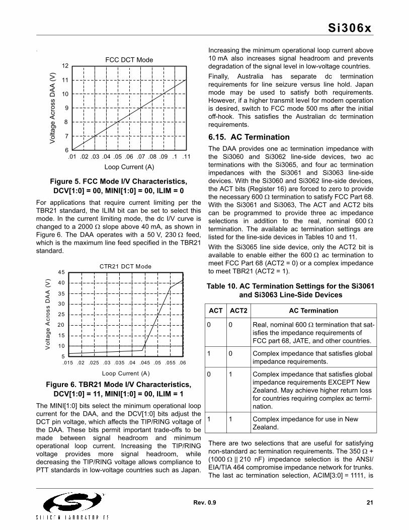
For applications that require current limiting per theTBR21 standard, the ILIM bit can be set to select thismode. In the current limiting mode, the dc I/V curve ischanged to a 2000 Ω slope above 40 mA, as shown inFigure 6. The DAA operates with a 50 V, 230 Ω feed,which is the maximum line feed specified in the TBR21standard.
Figure 6. TBR21 Mode I/V Characteristics,DCV[1:0] = 11, MINI[1:0] = 00, ILIM = 1
The MINI[1:0] bits select the minimum operational loopcurrent for the DAA, and the DCV[1:0] bits adjust theDCT pin voltage, which affects the TIP/RING voltage ofthe DAA. These bits permit important trade-offs to bemade between signal headroom and minimumoperational loop current. Increasing the TIP/RINGvoltage provides more signal headroom, whiledecreasing the TIP/RING voltage allows compliance toPTT standards in low-voltage countries such as Japan.
Increasing the minimum operational loop current above10 mA also increases signal headroom and preventsdegradation of the signal level in low-voltage countries.Finally, Australia has separate dc terminationrequirements for line seizure versus line hold. Japanmode may be used to satisfy both requirements.However, if a higher transmit level for modem operationis desired, switch to FCC mode 500 ms after the initialoff-hook. This satisfies the Australian dc terminationrequirements.
6.15. AC TerminationThe DAA provides one ac termination impedance withthe Si3060 and Si3062 line-side devices, two acterminations with the Si3065, and four ac terminationimpedances with the Si3061 and Si3063 line-sidedevices. With the Si3060 and Si3062 line-side devices,the ACT bits (Register 16) are forced to zero to providethe necessary 600 Ω termination to satisfy FCC Part 68.With the Si3061 and Si3063, The ACT and ACT2 bitscan be programmed to provide three ac impedanceselections in addition to the real, nominal 600 Ωtermination. The available ac termination settings arelisted for the line-side devices in Tables 10 and 11.With the Si3065 line side device, only the ACT2 bit isavailable to enable either the 600 Ω ac termination tomeet FCC Part 68 (ACT2 = 0) or a complex impedanceto meet TBR21 (ACT2 = 1).
There are two selections that are useful for satisfyingnon-standard ac termination requirements. The 350 Ω +(1000 Ω || 210 nF) impedance selection is the ANSI/EIA/TIA 464 compromise impedance network for trunks.The last ac termination selection, ACIM[3:0] = 1111, is
12
11
10
9
8
7
6.01 .02 .03 .04 .05 .06 .07 .08 .09 .1 .11
Loop Current (A)
FCC DCT ModeVo
ltage
Acr
oss
DAA
(V)
45
40
35
30
25
20
15
10
5.015 .02 .025 .03 .035 .04 .045 .05 .055 .06
Loop Current (A)
CTR21 DCT Mode
Vol
tage
Acr
oss
DA
A (
V)
Table 10. AC Termination Settings for the Si3061 and Si3063 Line-Side Devices
ACT ACT2 AC Termination
0 0 Real, nominal 600 Ω termination that sat-isfies the impedance requirements of FCC part 68, JATE, and other countries.
1 0 Complex impedance that satisfies global impedance requirements.
0 1 Complex impedance that satisfies global impedance requirements EXCEPT New Zealand. May achieve higher return loss for countries requiring complex ac termi-nation.
1 1 Complex impedance for use in New Zealand.

Si306x
22 Rev. 0.9
designed to satisfy minimum return loss requirementsfor every country in the world that requires a complextermination. For any of the ac termination settings, theprogrammable digital hybrid can be used to furtherreduce near-end echo. See the following “6.16.Transhybrid Balance” section for more details.
6.16. Transhybrid BalanceThe DAA contains an on-chip analog hybrid thatperforms the 2- to 4-wire conversion and near-end echocancellation. This hybrid circuit is adjusted for each actermination setting selected.
6.17. Ring DetectionThe ring signal is resistively coupled from TIP and RINGto the RNG1 and RNG2 pins. The DAA supports eitherfull- or half-wave ring detection. With full-wave ringdetection, the designer can detect a polarity reversal ofthe ring signal. See “6.24. Caller ID” on page 25. Thering detection threshold is programmable with the RT bit(Register 16, bit 0).The ring detector mode is controlled by the RFWE bit(Register 18). When the RFWE bit is 0 (default mode),the ring detector operates in half-wave rectifier mode. Inthis mode, only positive ring signals are detected. Apositive ring signal is defined as a voltage greater thanthe ring threshold across RNG1-RNG2. Conversely, anegative ring signal is defined as a voltage less than thenegative ring threshold across RNG1-RNG2. When theRFWE bit is 1, the ring detector operates in full-waverectifier mode. In this mode, both positive and negativering signals are detected.The ring detector output can be monitored in one of twoways. The first method uses the register bits RDTP,RDTN, and RDT (Register 5). The second method usesthe SDO output internal to the integrated system-sidemodule.The ring detector mode is controlled by the RFWE bit(Register 18). When the RFWE bit is 0 (default mode),the ring detector operates in half-wave rectifier mode. Inthis mode, only positive ring signals are detected. Apositive ring signal is defined as a voltage greater thanthe ring threshold across RNG1-RNG2. Conversely, anegative ring signal is defined as a voltage less than thenegative ring threshold across RNG1-RNG2. When theRFWE bit is 1, the ring detector operates in full-waverectifier mode. In this mode, both positive and negativering signals are detected.The first ring detect method uses the ring detect bits(RDTP, RDTN, and RDT). The RDTP and RDTNbehavior is based on the RNG1-RNG2 voltage. Whenthe signal on RNG1-RNG2 is above the positive ringthreshold the RDTP bit is set. When the signal on
RNG1-RNG2 is below the negative ring threshold theRDTN bit is set. When the signal on RNG1-RNG2 isbetween these thresholds, neither bit is set.The RDT behavior is also based on the RNG1-RNG2voltage. When the RFWE bit is 0, a positive ring signalsets the RFWE bit for a period of time. When the RFWEbit is 1, a positive or negative ring signal sets the RDTbit.The RDT bit acts like a one shot. When a new ringsignal is detected, the one shot is reset. If no new ringsignals are detected prior to the one shot counterreaching 0, then the RDT bit clears. The length of thiscount is approximately 5 seconds. The RDT bit is resetto 0 by an off-hook event. If the RDTM bit(Register 3, bit 7) is set, a hardware interrupt occurs onthe INT port when RDT is triggered. This interrupt canbe cleared by writing to the RDTI bit (Register 4, bit 7).When the RDI bit (Register 2, bit 2) is set, an interruptoccurs on both the beginning and end of the ring pulseas defined by the RTO bits (Register 23, bits 6:3). Ringvalidation may be enabled when using the RDI bit.The second ring detect method uses the serialcommunication interface to transmit ring data. If thecommunications link is active (PDL=0) and the device isnot off-hook or not in on-hook line monitor mode, thering data is presented on SDO. The waveform on SDOdepends on the state of the RFWE bit.When the RFWE bit is 0, SDO is –32768 (8000h) whenthe RNG1-RNG2 voltage is between the thresholds. Onring detection, SDO transitions to +32767 when the ringsignal is positive, then goes back to –32768 when thering is near 0 and negative. Therefore, a near squarewave is presented on SDO that swings from –32768 to+32767 in cadence with the ring signal.When the RFWE bit is 1, SDO sits at approximately+1228 when the RNG1-RNG2 voltage is between thethresholds. When the ring becomes positive, SDOtransitions to +32767. When the ring signal is near 0,SDO remains near 1228. As the ring signal becomesnegative, the SDO transitions to –32768. This repeats incadence with the ring signal.To observe the ring signal on SDO, observe the MSB ofthe data. The MSB toggles at the same frequency asthe ring signal independent of the ring detector mode.This method is adequate for determining the ringfrequency.
6.18. Ring ValidationThis feature prevents false triggering of a ring detectionby validating the ring parameters. Invalid signals, suchas a line voltage change when a parallel handset goesoff-hook, pulse dialing, or a high-voltage line test are

Si306x
Rev. 0.9 23
ignored. Ring validation can be enabled during normaloperation and in low power sleep mode. The externalMCLK signal is required in low power sleep mode forring validation.The ring validation circuit operates by calculating thetime between alternating crossings of positive andnegative ring thresholds to validate that the ringfrequency is within tolerance. High and low frequencytolerances are programmable in the RAS[5:0] andRMX[5:0] fields. The RCC[2:0] bits define how long thering signal must be within tolerance.Once the duration of the ring frequency is validated bythe RCC bits, the circuitry stops checking for frequencytolerance and begins checking for the end of the ringsignal, which is defined by a lack of additional thresholdcrossings for a period of time configured by theRTO[3:0] bits. When the ring frequency is first validated,a timer defined by the RDLY[2:0] bits is started. If theRDLY[2:0] timer expires before the ring timeout, thenthe ring is validated and a valid ring is indicated. If thering timeout expires before the RDLY[2:0] timer, a validring is not indicated.Ring validation requires five parameters:
Timeout parameter to place a lower limit on the frequency of the ring signal on the RAS[5:0] bits (Register 24). The frequency is measured by calculating the time between crossings of positive and negative ring thresholds.Minimum count to place an upper limit on the frequency on the RMX[5:0] bits (Register 22).Time interval over which the ring signal must be the correct frequency on the RCC[2:0] bits (Register 23).Timeout period that defines when the ring pulse has ended based on the most recent ring threshold crossing.Delay period between when the ring signal is validated and when a valid ring signal is indicated to accommodate distinctive ringing.
The RNGV bit (Register 24, bit 7) enables or disablesthe ring validation feature in normal operating mode andlow-power sleep mode.
6.19. Ringer Impedance and ThresholdThe ring detector in many DAAs is ac coupled to the linewith a large 1 µF, 250 V decoupling capacitor. The ringdetector on the Si306x DAA is resistively coupled to theline. This coupling produces a high ringer impedance tothe line of approximately 20 MΩ to meet the majority ofcountry PTT specifications, including FCC and TBR21. Several countries including Poland, South Africa, andSlovenia, require a maximum ringer impedance that canbe met with an internally synthesized impedance by
setting the RZ bit (Register 16, bit 1).Some countries also specify ringer thresholdsdifferently. The RT bit (Register 16, bit 0) selectsbetween two different ringer thresholds: 15 V ±10% and21.5 V ±10%. These two settings satisfy ringerthreshold requirements worldwide. The thresholds areset so that a ring signal is guaranteed to not be detectedbelow the minimum, and a ring signal is guaranteed tobe detected above the maximum.
6.20. Pulse Dialing and Spark QuenchingPulse dialing results from going off- and on-hook togenerate make and break pulses. The nominal rate is10 pulses per second. Some countries have strictspecifications for pulse fidelity that include make andbreak times, make resistance, and rise and fall times. Ina traditional solid-state dc holding circuit, there aremany problems in meeting these requirements. The Si306x dc holding circuit actively controls the on-hook and off-hook transients to maintain pulse dialingfidelity. Spark quenching requirements in countries such asItaly, the Netherlands, South Africa, and Australia dealwith the on-hook transition during pulse dialing. Thesetests provide an inductive dc feed resulting in a largevoltage spike. This spike is caused by the lineinductance and the sudden decrease in current throughthe loop when going on-hook. The traditional solution tothe problem is to put a parallel resistive capacitor (RC)shunt across the hookswitch relay. However, thecapacitor required is large (~1 µF, 250 V) and relativelyexpensive. In the Si306x, loop current can be controlledto achieve three distinct on-hook speeds to pass sparkquenching tests without additional BOM components.Through the settings of four bits in three registers, OHS(Register 16), OHS2 (Register 31), SQ1 and SQ0(Register 59), a slow ramp down of loop current can beachieved which induces a delay between the time OHbit is cleared and the time the DAA actually goes on-hook.To ensure proper operation of the DAA during pulsedialing, disable the automatic resistor calibration that isperformed each time the DAA enters the off-hook stateby setting the RCALD bit (Register 25, bit 5).
6.21. Billing Tone Detection and Receive Overload
“Billing tones” or “metering pulses” generated by theCentral Office can cause modem connection difficulties.The billing tone is typically either a 12 or 16 kHz signaland is sometimes used in Germany, Switzerland, andSouth Africa. Depending on line conditions, the billingtone might be large enough to cause major errors in the

Si306x
24 Rev. 0.9
line data. The DAA can provide feedback indicating thebeginning and end of a billing tone.Billing tone detection is enabled with the BTE bit(Register 17, bit 2). Billing tones less than 1.1 VPK onthe line are filtered out by the low pass digital filter of theDAA. The ROV bit is set when a line signal is greaterthan 1.1 VPK, indicating a receive overload condition.The BTD bit is set when a billing tone is large enough toexcessively reduce the line-derived power supply of theline-side device.The OVL bit (Register 19) can be polled following abilling tone detection. The OVL bit indicates that thebilling tone has passed when it returns to 0. The ROVbit is sticky and must be written to 0 to be reset. Afterthe billing tone passes, the DAA initiates an auto-calibration sequence that must complete before datacan be transmitted or received.Certain line events, such as an off-hook event on aparallel phone or a polarity reversal, can trigger the ROVor the BTD bits. Look for multiple events beforequalifying if billing tones are present. After the billingtone passes, the DAA initiates an auto-calibrationsequence that must complete before data can betransmitted or received.Although the DAA remains off-hook during a billing toneevent, the received data from the line is corrupted whena large billing tone occurs. If the user wishes to receivedata through a billing tone, an external LC filter must beadded. A manufacturer can provide this filter to users inthe form of a dongle that connects on the phone linebefore the DAA. This prevents the manufacturer fromhaving to include a costly LC filter to support multiplecountries and customers.Alternatively, when a billing tone is detected, the systemsoftware notifies the user that a billing tone hasoccurred. Notification prompts the user to contact thetelephone company to disable billing tones or topurchase an external LC filter.Disturbances on the line other than billing tones canalso cause a receive overload. Some conditions mayresult in a loop current collapse to a level below theminimum required operating current of the DAA. Whenthis occurs, the dropout detect bit (DOD) is set, and aninterrupt will be generated if the dropout detect interruptmask bit (DODM) is set.
6.22. Billing Tone Filter (Optional)To operate without degradation during billing tones inGermany, Switzerland, and South Africa, requires anexternal LC notch filter. The Si306x can remain off-hookduring a billing tone event, but line data is lost in thepresence of large billing tone signals. The notch filter
design requires two notches, one at 12 kHz and one at16 kHz. Because these components are expensive andfew countries utilize billing tones, this filter is typicallyplaced in an external dongle or added as a populationoption for these countries. Figure 7 shows an examplebilling tone filter.
Figure 7. Billing Tone FilterL1 must carry the entire loop current. The seriesresistance of the inductors is important to achieve anarrow and deep notch. This design has more than25 dB of attenuation at both 12 kHz and 16 kHz.
The billing tone filter affects the DAA’s ac terminationand return loss. The global complex ac termination(ACIM = 1111) passes global return loss specificationswith and without the billing tone filter by at least 3 dB.This ac termination is optimized for frequency responseand hybrid cancellation and has greater than 4 dB ofmargin with or without the dongle for South Africa,Australia, TBR21, Germany, and Switzerland countryspecifications.
6.23. On-Hook Line MonitorThe on-hook line monitor mode allows the Si306x toreceive line activity when in an on-hook state. This
Table 11. Component Values—Optional Billing Tone Filters
Symbol Value
C1,C2 0.027 µF, 50 V, ±10%
C3 0.01 µF, 250 V, ±10%
L1 3.3 mH, >120 mA, <10 Ω, ±10%
L2 10 mH, >40 mA, <10 Ω, ±10%
L2
C3
RING
TIP
FromLine
ToDAA
C1
C2
L1

Si306x
Rev. 0.9 25
mode is typically used to detect caller ID data and isenabled by setting the ONHM bit (Register 5, bit 3).Caller ID data can be gained up or attenuated using thereceive gain control bits in Register 15.
6.24. Caller IDWith the Si306x, caller ID data can be passed from thephone line to a caller ID decoder connected to the serialport.6.24.1. Type I Caller IDType I Caller ID sends the CID data while the phone ison-hook.In systems where the caller ID data is passed on thephone line between the first and second rings, utilize thefollowing method to capture the caller ID data:1. After identifying a ring signal using one of the
methods described in "6.17. Ring Detection" on page 22, determine when the first ring is complete.
2. Assert the ONHM bit (Register 5, bit 3) to enable caller ID data detection. The caller ID data passed across the RNG 1/2 pins is presented to the host via the SDO pin.
3. Clear the ONHM bit after the caller ID data is received.
In systems where the caller ID data is preceded by aline polarity (battery) reversal, use the following methodto capture the caller ID data:1. Enable full wave rectified ring detection (RFWE,
Register 18, bit 1).2. Monitor the RDTP and RDTN register bits to identify
if a polarity reversal or a ring signal has occurred. A polarity reversal trips either the RDTP or RDTN ring detection bits, and thus the full-wave ring detector must be used to distinguish a polarity reversal from a ring. The lowest specified ring frequency is 15 Hz; therefore, if a battery reversal occurs, the DSP should wait a minimum of 40 ms to verify that the event observed is a battery reversal and not a ring signal. This time is greater than half the period of the longest ring signal. If another edge is detected during this 40 ms pause, this event is characterized as a ring signal and not a battery reversal.
3. Assert the ONHM bit (Register 5, bit 3) to enable caller ID data detection. The caller ID data passed across the RNG 1/2 pins is presented to the data to the host via the SDO pin.
4. Clear the ONHM bit after the caller ID data is received.
6.24.2. Type II Caller ID (Si3063 and Si3064 Line-Side Devices Only)
Type II Caller ID sends the CID data while the phone isoff-hook and is often referred to as caller ID/call waiting(CID/CW). To receive the CID data while off-hook, usethe following procedure (see Figure 8):1. The Caller Alert Signal (CAS) tone is sent from the
Central Office (CO) and is digitized along with the line data. The host processor must detect the presence of this tone.
2. The DAA must then check for another parallel device on the same line. This is accomplished by briefly going on-hook, measuring the line voltage, and then returning to an off-hook state.a. Set the CALD bit (Register 17, bit 5) to disable
the calibration that automatically occurs when going off-hook.
b. Set the RCALD bit (Register 25, bit 5) to disable the resistor calibration from occurring when going off-hook.
c. Set the FOH[1:0] bits (Register 31, bits 6:5) to 11 to reduce the off-hook counter time to 8 ms.
d. Clear the OH bit to put the DAA in an on-hook state. The RXM bit (Register 19, bit 3) may also be set to mute the receive path.
e. Read the LVS bits to determine the state of the line.If the LVS bits read the typical on-hook line voltage, then no parallel devices are active on the line and CID data reception can be continued.If the LVS bits read well below the typical on-hook line voltage, then one or more devices are present and active on the same line that are not compliant with Type II CID. Do not continue CID data reception.
f. Set the OH bit to 1 to return to an off-hook state. After returning to an off-hook state and waiting 8 ms for the off-hook counter, normal data transmission and reception can proceed. If a non-compliant parallel device is present, then a reply tone is not sent by the host tone generator and the CO does not proceed with sending the CID data. If all devices on the line are Type II CID compliant, then the host must mute its upstream data output to avoid propagation of its reply tone and the subsequent CID data. After muting its upstream data output, the host processor should then return an acknowledgement (ACK) tone to the CO to request the transmission of the CID data.

Si306x
26 Rev. 0.9
3. The CO then responds with the CID data. After receiving the CID data, the host processor unmutes the upstream data output and continues with normal operation.
4. The muting of the upstream data path by the host processor mutes the handset in a telephone application so the user cannot hear the acknowledgement tone and CID data being sent.
5. The CALD and RCALD bits can be cleared to re-enable the automatic calibration when going off-hook. The FOH[1:0] bits also can be programmed to 01 to restore the default off-hook counter time.
Because of the nature of the low-power ADC, the datapresented on SDO could have up to a 10% dc offset.The caller ID decoder must either use a high pass or aband pass filter to accurately retrieve the caller ID data.
6.25. Overload DetectionThe Si306x can be programmed to detect an overloadcondition that exceeds the normal operating powerrange of the DAA circuit. To use the overload detectionfeature, the following steps should be followed:1. Set the OH bit (Register 5, bit 0) to go off-hook, and
wait 25 ms to allow line transients to settle.2. Enable overload detection by then setting the OPE
bit (Register 17, bit 3).If the DAA senses an overload situation, it automaticallypresents an 800 Ω impedance to the line to reduce the
hookswitch current. At this time, the DAA also sets theOPD bit (Register 19, bit 0) to indicate that an overloadcondition exists. The line current detector within theDAA has a threshold that is dependant upon the ILIM bit(Register 26). When ILIM = 0, the overload detectionthreshold equals 160 mA. When ILIM = 1, the overloaddetection threshold equals 60 mA. The OPE bit shouldalways be cleared before going off-hook.
6.26. Gain ControlThe DAA supports different gain and attenuationsettings depending on the line-side device being used.For all line-side devices, gains of 0, 3, 6, 9, and 12 dBcan be selected for the receive path with the ARX[2:0]bits. The receive path can also be muted with the RXMbit. Attenuations of 0, 3, 6, 9, and 12 dB can also beselected for the transmit path with the ATX[2:0] bits. Thetransmit path also can be muted with the TXM bit.The signal flow through the DAA line-side andintegrated module is shown in Figures 9 and 10.
6.27. Clock Generation The Si306x line-side device connects to a system-sidemodule that is in turn integrated into a host processor.The Si306x line-side receives all clocking from thismodule and does not need any other clock inputs. Thesample rate for the Si306x is controlled by the SampleRate Control Register.
Figure 8. Implementing Type II Caller ID on the Si306x
Notes:1. The off-hook counter and calibrations prevent transmission or reception of data for 402.75 ms (default) for the line
voltage to settle.2. The caller alert signal (CAS) tone transmits from the CO to signal an incoming call.3. The device is taken on-hook to read the line voltage in the LVS bits to detect parallel handsets. In this mode, no data is
transmitted on the SDO pin.4. When the device returns off-hook, the normal off-hook counter is reduced to 8 ms. If the CALD and RCALD bits are set,
then the automatic calibrations are not performed.5. After allowing the off-hook counter to expire (8 ms), normal transmission and reception can continue. If CID data
reception is required, send the appropriate signal to the CO at this time.
FOH[1] Bit
RCALD Bit
CALD Bit
OH Bit
FOH[0] Bit
CAS T one
Rece ivedOn-Hook Of f -H ook C ounter
(8 m s )O ff-Hook A c kLINE On-Hook
Off-Hook Counter and Calibration
(402.75 ms nominally) O ff-Hook
1 2 3 4

Si306x
Rev. 0.9 27
Figure 9. Si306x Signal Flow Diagram
Figure 10. Embedded System-Side DAA Module Signal Flow Diagram
To EmbeddedSystem-SideDAA Module
ADC
DAC
Link AnalogHybrid
ACT TX
CO
DigitalHybrid
IIREDigitalFilter1
To Line-SideDeviceLink
ATX orTXG
ARX orRXG
IIREDigitalFilter1
5/200 HzLPF
Pole2
SDI
SDO
Notes:1. Available with 32.768 MHz embedded system-side DAA module only.2. Available with Si3064 line-side device.

Si306x
28 Rev. 0.9
7. Control RegistersTable 12. Register Summary
Register Name Bit 7 Bit 6 Bit 5 Bit 4 Bit 3 Bit 2 Bit 1 Bit 01 Control 1 SR PWMM[1:0] IDL2 Control 2 INTE INTP WDTEN RDI HBE RXE3 Interrupt Mask RDTM ROVM FDTM BTDM DODM LCSOM POLM1
4 Interrupt Source RDTI ROVI FDTI BTDI DODI LCSOI POLI1
5 DAA Control 1 RDTN RDTP ONHM RDT OHE OH6 DAA Control 2 PDL PDN7 Sample Rate Control SRC[3:0]8 Reserved9 Reserved10 DAA Control 3 DDL11 System-Side and Line-Side LSID[3:0] REVA[3:0]12 Line-Side Device Status FDT LCS[4:0]13 Line-Side Device Revision 1 REVB[3:0]14 Reserved15 TX/RX Gain Control 1 TXM ATX[2:0] RXM ARX[2:0]16 International Control 1 ACT22 OHS ACT2 IIRE3 RZ RT17 International Control 2 CALZ MCAL CALD OPE BTE ROV BTD18 International Control 3 RFWE19 International Control 4 OVL DOD OPD20 Call Progress RX Attenuation ARM[7:0]21 Call Progress TX Attenuation ATM[7:0]22 Ring Validation Control 1 RDLY[1:0] RMX[5:0]23 Ring Validation Control 2 RDLY[2] RTO[3:0] RCC[2:0]24 Ring Validation Control 3 RNGV RAS[5:0]25 Resistor Calibration RCALS RCALM RCALD RCAL[3:0]26 DC Termination Control DCV[1:0] MINI[1:0] Reserved ILIM DCR27 Reserved28 Loop Current Status LCS2[7:0]1
29 Line Voltage Status LVS[7:0]1
30 Reserved31 DAA Control 4 FOH[1:0] OHS2 FILT LVFD1
32–42 Reserved43 Line Current/Voltage Threshold
InterruptCVT[7:0]1
44 Line Current/Voltage Threshold Interrupt Control CVI1 CVS1 CVM1 CVP1
45–58 Reserved59 Spark Quenching Control SQ1 SQ0 RG1 GCE
Notes:1. Bit is available for Si3062, Si3063, and Si3064 line-side devices only.2. Bit is available for Si3061 and Si3063 line-side devices only.3. Bit is available with 32.768 MHz system-side module only.

Si306x
Rev. 0.9 29
Reset settings = 0000_0000
Register 1. Control 1
Bit D7 D6 D5 D4 D3 D2 D1 D0
Name SR PWMM[1:0] IDL
Type R/W R/W R/W
Bit Name Function
7 SR Software Reset. 0 = Enables the DAA for normal operation. 1 = Sets all registers to their reset value.Note: Bit automatically clears after being set.
6 Reserved Read returns zero.
5:4 PWMM[1:0] Pulse Width Modulation Mode.Refer to PWMM bit description in the embedded system-side module specification for operation of these bits. The PWM output signals depends on the input clock frequency provided to the SiLabs system-side module.
3:2 Reserved Read returns zero.
1 IDL Isolation Digital Loopback. 0 = Digital loopback across the isolation barrier is disabled.1 = Enables digital loopback mode across the isolation barrier. The line-side device must be enabled and off-hook before setting this mode. This data path includes the TX and RX filters.
0 Reserved Read returns zero.

Si306x
30 Rev. 0.9
Reset settings = 0000_0011
Register 2. Control 2
Bit D7 D6 D5 D4 D3 D2 D1 D0
Name INTE INTP WDTEN RDI HBE RXE
Type R/W R/W R/W R/W R/W R/W
Bit Name Function
7 INTE Interrupt Pin Enable.0 = The INT port is disabled.1 = The INT port is enabled.
6 INTP Interrupt Polarity Select.0 = The INT port is active low. 1 = The INT port is active high.
5 Reserved Returns to zero.
4 WDTEN Watchdog Timer Enable.When set, this bit can only be cleared by a hardware reset. The watchdog timer monitors register accesses. If no register accesses occur within a 4 second window, the DAA is put into an on-hook state. A write of a DAA register restarts the watchdog timer counter. If the watchdog timer times out, the OH bit is cleared, placing the DAA into an on-hook state. Setting the OH bit places the DAA back into an off-hook state.0 = Watchdog timer disabled.1 = Watchdog timer enabled.
3 Reserved Returns to zero.
2 RDI Ring Detect Interrupt Mode.This bit operates in conjunction with the RDTM and RDTI bits. This bit is selected if one or two interrupts are generated for every ring burst.0 = An interrupt is generated at the beginning of every ring burst.1 = An interrupt is generated at the beginning and end of every ring burst. The interrupt at the beginning of the ring burst must be serviced (by writing a 0 to the RDTI bit) before the end of the ring burst for both interrupts to occur.
1 HBE Hybrid Enable.0 = Disconnects hybrid in transmit path.1 = Connects hybrid in transmit path.
0 RXE Receive Enable.0 = Receive path disabled.1 = Enables receive path.

Si306x
Rev. 0.9 31
Reset settings = 0000_0000
Register 3. Interrupt Mask
Bit D7 D6 D5 D4 D3 D2 D1 D0
Name RDTM ROVM FDTM BTDM DODM LCSOM POLM
Type R/W R/W R/W R/W R/W R/W R/W
Bit Name Function
7 RDTM Ring Detect Mask.0 = A ring signal does not cause an interrupt on the INT port.1 = A ring signal causes an interrupt on the INT port.
6 ROVM Receive Overload Mask.0 = A receive overload does not cause an interrupt on the INT port.1 = A receive overload causes an interrupt on the INT port.
5 FDTM Frame Detect Mask.0 = The communications link achieving frame lock does not cause an interrupt on the INT port.1 = The communications link achieving frame lock causes an interrupt on the INT port.
4 BTDM Billing Tone Detect Mask.0 = A detected billing tone does not cause an interrupt on the INT port.1 = A detected billing tone causes an interrupt on the INT port.
3 DODM Drop Out Detect Mask.0 = A line supply dropout does not cause an interrupt on the INT port.1 = A line supply dropout causes an interrupt on the INT port.
2 LCSOM Loop Current Sense Overload Mask.0 = An interrupt does not occur when the LCS bits are all 1s.1 = An interrupt occurs when the LCS bits are all 1s.
1 Reserved Read returns zero.
0 POLM Polarity Reversal Detect Mask (Si3062, Si3063, and Si3065 line-side devices only).Generated from bit 7 of the LVS register. When this bit transitions, it indicates that the polarity of TIP and RING was switched.0 = A polarity change on TIP and RING does not cause an interrupt on the INT port.1 = A polarity change on TIP and RING causes an interrupt on the INT port.

Si306x
32 Rev. 0.9
Reset settings = 0000_0000
Register 4. Interrupt Source
Bit D7 D6 D5 D4 D3 D2 D1 D0Name RDTI ROVI FDTI BTDI DODI LCSOI POLIType R/W R/W R/W R/W R/W R/W R/W
Bit Name Function7 RDTI Ring Detect Interrupt.
0 = A ring signal is not occurring.1 = A ring signal is detected. If the RDTM (Register 3) and INTE (Register 2) bits are set a hard-ware interrupt occurs on the INT port. This bit must be written to a 0 to be cleared. The RDI bit (Register 2) determines if this bit is set only at the beginning of a ring pulse, or at the end of a ring pulse as well. This bit should be cleared after clearing the PDL bit (Register 6) because powering up the line-side device may cause this interrupt to be triggered.
6 ROVI Receive Overload Interrupt.0 = An excessive input level on the receive pin is not occurring.1 = An excessive input level on the receive pin is detected. If the ROVM and INTE bits are set a hardware interrupt occurs on the INT port. This bit must be written to 0 to clear it. This bit is iden-tical in function to the ROV bit (Register 17). Clearing this bit also clears the ROV bit.
5 FDTI Frame Detect Interrupt. 0 = Frame detect is established on the communications link.1 = This bit is set when the communications link does not have frame lock. If the FDTM and INTE bits are set, a hardware interrupt occurs on the INT port. Once set, this bit must be written to a 0 to be cleared.
4 BTDI Billing Tone Detect Interrupt.0 = A billing tone has not occurred.1 = A billing tone has been detected. If the BTDM and INTE bits are set, a hardware interrupt occurs on the INT port. This bit must be written to 0 to clear it.
3 DODI Drop Out Detect Interrupt. 0 = The line-side power supply has not collapsed.1 = The line-side power supply has collapsed. (The DOD bit in Register 19 has fired.) If the DODM and INTE bits are set, a hardware interrupt occurs on the INT port. This bit must be writ-ten to 0 to clear it. This bit should be cleared after clearing the PDL bit (Register 6) because powering as the line-side device can cause this interrupt to be triggered.
2 LCSOI Loop Current Sense Overload Interrupt. 0 = The LCS bits have not reached max (all ones).1 = The LCS bits have reached max value. If the LCSOM bit (Register 3) and the INTE bit are set, a hardware interrupt occurs on the INT port. This bit must be written to 0 to clear it.LCSOI does not necessarily imply that an overcurrent situation has occurred. An overcurrent sit-uation in the DAA is determined by the status of the OPD bit (Register 19). After the LCSOI interrupt fires, the OPD bit should be checked to determine if an overcurrent situation exists.
1 Reserved Read returns zero.0 POLI Polarity Reversal Detect Interrupt (Si3062, Si3063, and Si3065 line-side devices only).
0 = Bit 7 of the LVS register does not change states.1 = Bit 7 of the LVS register changes from a 0 to a 1, or from a 1 to a 0, indicating the polarity of TIP and RING is switched. If the POLM and INTE bits are set, a hardware interrupt occurs on the INT port. To clear the interrupt, write this bit to 0.

Si306x
Rev. 0.9 33
Reset settings = 0000_0000
Register 5. DAA Control 1
Bit D7 D6 D5 D4 D3 D2 D1 D0
Name RDTN RDTP ONHM RDT OH
Type R R R/W R R/W
Bit Name Function
7 Reserved Read returns zero.
6 RDTN Ring Detect Signal Negative.0 = No negative ring signal is occurring.1 = A negative ring signal is occurring.
5 RDTP Ring Detect Signal Positive.0 = No positive ring signal is occurring.1 = A positive ring signal is occurring.
4 Reserved Read returns zero.
3 ONHM On-Hook Line Monitor.0 = Normal on-hook mode.1 = Enables low-power on-hook monitoring mode allowing the host to receive line activity without going off-hook. This mode is used for caller-ID detection.
2 RDT Ring Detect.0 = Reset 5 seconds after last positive ring is detected or when the system executes an off-hook. Only a positive ring sets this bit when RFWG = 0. When RFWG = 1, either a positive or negative ring sets this bit.1 = Indicates a ring is occurring.
1 Reserved Read returns zero.
0 OH Off-Hook.0 = Line-side device on-hook.1 = Causes the line-side device to go off-hook. This bit operates independently of the OHE bit and is a logic OR with the off-hook pin when enabled.

Si306x
34 Rev. 0.9
Reset settings = 0001_0000
Register 6. DAA Control 2
Bit D7 D6 D5 D4 D3 D2 D1 D0
Name PDL PDN
Type R/W R/W
Bit Name Function
7:5 Reserved Read returns zero.
4 PDL Powerdown Line-Side Device.0 = Normal operation. Program the clock generator before clearing this bit.1 = Places the line-side device in lower power mode.
3 PDN Powerdown System-Side Module.0 = Normal operation.1 = Powers down the system-side device. A pulse on RESET is required to restore normal operation.
2:0 Reserved Read returns zero.

Si306x
Rev. 0.9 35
Reset settings = 0000_0000
Register 7. Sample Rate Control
Bit D7 D6 D5 D4 D3 D2 D1 D0
Name SRC[3:0]
Type R/W
Bit Name Function
7:4 Reserved Read returns zero.
3:0 SRC[3:0] Sample Rate Control.Sets the sample rate of the line-side device.The following sample rate settings are available with either the 32.4 MHz or the 32.768 MHz system-side modules:0000 = 7200 Hz0001 = 8000 Hz0010 = 8229 Hz0011 = 8400 Hz0100 = 9000 Hz0101 = 9600 Hz0110 = 10286 HzThe following sample rate settings are only available with the 32.768 MHz system-sidemodule and are otherwise reserved bits (read returns zero):0111 = 12000 Hz1000 = 13714 Hz1001 = 16000 HzFor all system-side modules:1010–1111 = reserved

Si306x
36 Rev. 0.9
Reset settings = 0000_0000
Reset settings = 0000_0000
Register 8-9. Reserved
Bit D7 D6 D5 D4 D3 D2 D1 D0
Name
Type
Bit Name Function
7:0 Reserved Read returns zero.
Register 10. DAA Control 3
Bit D7 D6 D5 D4 D3 D2 D1 D0
Name DDL
Type R/W
Bit Name Function
7:1 Reserved Read returns zero.
0 DDL Digital Data Loopback.0 = Normal operation.1 = Takes data received on DRX and loops it back out to DTX before the TX and RX filters. Output data is identical to input data.

Si306x
Rev. 0.9 37
Reset settings = xxxx_xxxx
Reset settings = 0000_0000
Register 11. System-Side and Line-Side
Bit D7 D6 D5 D4 D3 D2 D1 D0
Name LSID[3:0] REVA[3:0]
Type R R
Bit Name Function
7:4 LSID[3:0] Line-Side ID Bits.These four bits will always read one of the following values depending on which line-side device is used. LSID[3:0]Si3060 1000Si3061 1001Si3062 1010Si3063 1011Si3064 0111Si3065 0110
3:0 REVA[3:0] System-Side Revision.Four-bit value indicating the revision of the system-side device.
Register 12. Line-Side Device Status
Bit D7 D6 D5 D4 D3 D2 D1 D0
Name FDT LCS[4:0]
Type R R
Bit Name Function
7 Reserved Read returns zero.
6 FDT Frame Detect. 0 = Indicates the communications link has not established frame lock.1 = Indicates the communications link frame lock is established.
5 Reserved Read returns zero.
4:0 LCS[4:0] Loop Current Sense.5-bit value returning the loop current when the DAA is in an off-hook state. 00000 = Loop current is less than required for normal operation.00100 = Minimum loop current for normal operation.11111 = Loop current is >127 mA, and a current overload condition may exist.

Si306x
38 Rev. 0.9
Reset settings = xxxx_xxxx
Reset settings = 0000_0000
Register 13. Line-Side Device Revision
Bit D7 D6 D5 D4 D3 D2 D1 D0
Name 1 REVB[3:0]
Type R
Bit Name Function
7 Reserved Read returns zero.
6 1 This bit always reads a one.
5:2 REVB[3:0] Line-Side Device Revision.Four-bit value indicating the revision of the line-side device.
1:0 Reserved Read returns zero.
Register 14. Reserved
Bit D7 D6 D5 D4 D3 D2 D1 D0
Name
Type
Bit Name Function
7:0 Reserved Read returns zero.

Si306x
Rev. 0.9 39
Reset settings = 0000_0000
Register 15. TX/RX Gain Control 1
Bit D7 D6 D5 D4 D3 D2 D1 D0
Name TXM ATX[2:0] RXM ARX[2:0]
Type R/W R/W R/W R/W
Bit Name Function
7 TXM Transmit Mute. 0 = Transmit signal is not muted.1 = Mutes the transmit signal.
6:4 ATX[2:0] Analog Transmit Attenuation.000 = 0 dB attenuation001 = 3 dB attenuation010 = 6 dB attenuation011 = 9 dB attenuation1xx = 12 dB attenuation
3 RXM Receive Mute. 0 = Receive signal is not muted.1 = Mutes the receive signal.
2:0 ARX[2:0] Analog Receive Gain.000 = 0 dB gain001 = 3 dB gain010 = 6 dB gain011 = 9 dB gain1xx = 12 dB gain

Si306x
40 Rev. 0.9
Reset settings = 0000_0000
Register 16. International Control 1
Bit D7 D6 D5 D4 D3 D2 D1 D0
Name ACT2 OHS ACT IIRE RZ RT
Type RW R/W R/W R/W R/W R/W
Bit Name Function
7 ACT2 AC Termination Select 2.Works with the ACT bit to select one of four ac terminations.Si3061 and Si3063 Settings:ACT2 ACT AC Termination0 0 Real, 600 Ω0 1 Global complex impedance1 0 TBR21 complex impedance1 1 New Zealand complex impedanceSi3065 Settings:ACT2 ACT AC Termination0 0 Real, 600 Ω0 1 TBR21 complex impedance1 0 TBR21 complex impedance1 1 Real, 600 ΩSi3060 and Si3062 Settings:ACT2 ACT AC TerminationX X Real, 600 ΩThe global complex impedance meets minimum return loss requirements in countries that require a complex ac termination. For improved return loss performance, the other complex impedances can be used.
6 OHS On-Hook Speed.This bit, in combination with the OHS2 bit and the SQ[1:0] bits, sets the amount of time for the line-side device to go on-hook. The on-hook speeds specified are measured from the time the OH bit is cleared until loop current equals zero. Si3061 and Si3063 Settings:OHS OHS2 SQ[1:0] Mean On-Hook Speed0 0 00 Less than 0.5 ms0 1 00 3 ms ±10% (meets ETSI standard)1 X 11 26 ms ±10% (meets Australia spark quenching spec)
Si3060, Si3062, and Si3065 Settings:OHS OHS2 SQ[1:0] Mean On-Hook SpeedX X XX Less than 0.5 ms
5 ACT AC Termination Select.Works with the ACT2 bit to select one of four ac terminations. See ACT2 description above.
4 IIRE IIR Filter Enable (32.768 MHz System-Side Module only).0 = FIR filter enabled for transmit and receive filters.1 = IIR filter enabled for transmit and receive filters.Refer to Figures 3–6 in the 32.768 MHz embedded system-side DAA module specification.

Si306x
Rev. 0.9 41
3:2 Reserved Read returns zero.
1 RZ Ringer Impedance.Si3061 and Si3063 Settings:0 = Maximum (high) ringer impedance.1 = Synthesized ringer impedance. See "6.19. Ringer Impedance and Threshold" on page 23.Si3060, Si3062, and Si3065 Settings:X = Maximum (high) ringer impedance.
0 RT Ringer Threshold Select.This bit is used to satisfy country requirements on ring detection. Signals below the lower level do not generate a ring detection; signals above the upper level are guaranteed to gener-ate a ring detection.0 = 13.5 to 16.51 = 19.35 to 23.65Si3060, Si3062, and Si3065 Settings:X = 13.5 to 16.5 Vrms
Bit Name Function

Si306x
42 Rev. 0.9
Reset settings = 0000_0000
Register 17. International Control 2
Bit D7 D6 D5 D4 D3 D2 D1 D0
Name CALZ MCAL CALD OPE BTE ROV BTD
Type R/W R/W R/W R/W R/W R/W R
Bit Name Function7 CALZ Clear ADC Calibration.
0 = Normal operation.1 = Clears the existing calibration data. This bit must be written back to 0 after being set.
6 MCAL Manual ADC Calibration.0 = No calibration.1 = Initiate manual ADC calibration.
5 CALD ADC Auto-Calibration Disable.0 = Enable auto-calibration.1 = Disable auto-calibration.
4 Reserved Read returns zero or one.3 OPE Overload Protect Enable.
0 = Disabled.1 = Enabled.The OPE bit should always be cleared before going off-hook.
2 BTE Billing Tone Detect Enable.When set, the DAA can detect a billing tone signal on the line and maintain on off-hook state through the billing tone. If a billing tone is detected, the BTD bit (Register 17) is set to indicate the event. Writing this bit to zero clears the BTD bit.0 = Billing tone detection disabled. The BDT bit is not function.1 = Billing tone detection enabled. The BDT is functional.
1 ROV Receive Overload.This bit is set when the receive input has an excessive input level (i.e., receive pin goes below ground). Writing a zero to this location clears this bit and the ROVI bit (Register 4, bit 6).0 = Normal receive input level.1 = Excessive receive input level.
0 BTD Billing Tone Detected.This bit is set if a billing tone is detected. Writing a zero to BTE clears this bit.0 = No billing tone detected.1 = Billing tone detected.

Si306x
Rev. 0.9 43
Reset settings = 0000_0000
Register 18. International Control 3
Bit D7 D6 D5 D4 D3 D2 D1 D0
Name RFWE
Type R/W
Bit Name Function
7:2 Reserved Read returns zero or one.
1 RFWE Ring Detector Full Wave Rectifier Enable.When RNGV (Register 24) is disabled, this bit controls the ring detector mode and the assertion of the RGDT pin. When RNGV is enabled, this bit configures the RGDT pin to either follow the ringing signal detected by the ring validation circuit or to follow an unqualified ring detect one-shot signal initiated by a ring-threshold crossing and terminated by a fixed counter timeout of approximately five seconds.
RNGV RFWE RGDT0 0 Half wave0 1 Full wave1 0 Validated Ring Envelope1 1 Ring Threshold Crossing One-Shot
0 Reserved Read returns zero.

Si306x
44 Rev. 0.9
Reset settings = 0000_0000
Register 19. International Control 4
Bit D7 D6 D5 D4 D3 D2 D1 D0
Name OVL DOD OPD
Type R R R
Bit Name Function
7:3 Reserved Read returns zero.
2 OVL Receive Overload Detect.This bit has the same function as ROV in Register 17, but clears itself after the overload is removed. This bit is only masked by the off-hook counter and is not affected by the BTE bit.0 = Normal receive input level.1 = Excessive receive input level.
1 DOD Recal/Dropout Detect.When the line-side device is off-hook, it is powered from the line itself. This bit will read 1 when loop current is not flowing. For example, if the line-derived power supply collapses, such as when the line is disconnected, this bit is set to 1. When on-hook and the line-side device is enabled, this bit is set to 1.0 = Normal operation.1 = Line supply dropout detected when off-hook.
0 OPD Overload Protection Detect.This bit is used to indicate that the DAA has detected a loop current overload. The detector fir-ing threshold depends on the setting of the ILIM bit (Register 26).OPD ILIM Overcurrent Threshold Overcurrent Status0 0 160 mA No overcurrent condition exists0 1 60 mA No overcurrent condition exists1 0 160 mA An overcurrent condition has been detected1 1 60 mA An overcurrent condition has been detected

Si306x
Rev. 0.9 45
Reset settings = 0000_0000
Reset settings = 0000_0000
Register 20. Call Progress RX Attenuation
Bit D7 D6 D5 D4 D3 D2 D1 D0Name ARM[7:0]Type R/W
Bit Name Function7:0 ARM[7:0] AOUT Receive Path Attenuation.
When decremented from the default setting, these bits linearly attenuate the AOUT receive path signal used for call progress monitoring. Setting the bits to all 0s mutes the AOUT receive path.Attenuation = 20log(ARM[7:0]/64)1111_1111 = +12 dB (gain)0111_1111 = +6 dB (gain)0100_0000 = 0 dB0010_0000 = –6 dB (attenuation)0001_0000 = –12 dB...0000_0000 = Mute
Register 21. Call Progress TX Attenuation
Bit D7 D6 D5 D4 D3 D2 D1 D0Name ATM[7:0]Type R/W
Bit Name Function7:0 ATM[7:0] AOUT Transmit Path Attenuation.
When decremented from the default settings, these bits linearly attenuate the AOUT trans-mit path signal used for call progress monitoring. Setting the bits to all 0s mutes the AOUT transmit path.Attenuation = 20log(ATM[7:0]/64)1111_1111 = +12 dB (gain)0111_1111 = +6 dB (gain)0100_0000 = 0 dB0010_0000 = –6 dB (attenuation)0001_0000 = –12 dB...0000_0000 = Mute

Si306x
46 Rev. 0.9
Reset settings = 1001_0110
Register 22. Ring Validation Control 1
Bit D7 D6 D5 D4 D3 D2 D1 D0
Name RDLY[1:0] RMX[5:0]
Type R/W R/W
Bit Name Function
7:6 RDLY[1:0] Ring Delay Bits 1 and 0.These bits, in combination with the RDLY[2] bit (Register 23), set the amount of time between when a ring signal is validated and when a valid ring signal is indicated. RDLY[2] RDLY[1:0] Delay0 00 0 ms0 01 256 ms0 10 512 ms...1 11 1792 ms
5:0 RMX[5:0] Ring Assertion Maximum Count.These bits set the maximum ring frequency for a valid ring signal within a 10% margin of error. During ring qualification, a timer is loaded with the RAS[5:0] field upon a TIP/RING event and decrements at a regular rate. When a subsequent TIP/RING event occurs, the timer value is compared to the RMX[5:0] field and if it exceeds the value in RMX[5:0] then the frequency of the ring is too high and the ring is invalidated. The difference between RAS[5:0] and RMX[5:0] identifies the minimum duration between TIP/RING events to qual-ify as a ring, in binary-coded increments of 2.0 ms (nominal). A TIP/RING event typically occurs twice per ring tone period. At 20 Hz, TIP/RING events would occur every 1/(2 x 20 Hz) = 25 ms. To calculate the correct RMX[5:0] value for a frequency range [f_min, f_max], the following equation should be used:
To compensate for error margin and ensure a sufficient ring detection window, it is recom-mended that the calculated value of RMX[5:0] be incremented by 1.
RMX 5:0[ ] RAS 5:0[ ] 12 f_max× 2 ms×--------------------------------------------- RMX RAS≤,–≥

Si306x
Rev. 0.9 47
Reset settings = 0010_1101
Register 23. Ring Validation Control 2
Bit D7 D6 D5 D4 D3 D2 D1 D0
Name RDLY[2] RTO[3:0] RCC[2:0]
Type R/W R/W R/W
Bit Name Function7 RDLY[2] Ring Delay Bit 2.
This bit, in combination with the RDLY[1:0] bits (Register 22), set the amount of time between when a ring signal is validated and when a valid ring signal is indicated.RDLY[2] RDLY[1:0] Delay0 00 0 ms0 01 256 ms0 10 512 ms...1 11 1792 ms
6:3 RTO[3:0] Ring Timeout.These bits set when a ring signal is determined to be over after the most recent ring thresh-old crossing.RTO[3:0] Ring Timeout0000 80 ms0001 128 ms0010 256 ms...1111 1920 ms
2:0 RCC[2:0] Ring Confirmation Count.These bits set the amount of time that the ring frequency must be within the tolerances set by the RAS[5:0] bits and the RMX[5:0] bits to be classified as a valid ring signal.RCC[2:0] Ring Confirmation Count Time000 100 ms001 150 ms010 200 ms011 256 ms100 384 ms101 512 ms110 640 ms111 1024 ms

Si306x
48 Rev. 0.9
Reset settings = 0001_1001
Register 24. Ring Validation Control 3
Bit D7 D6 D5 D4 D3 D2 D1 D0
Name RNGV RAS[5:0]
Type R/W R/W
Bit Name Function
7 RNGV Ring Validation Enable.0 = Ring validation feature is disabled.1 = Ring validation feature is enabled in both normal operating mode and low-power mode.
6 Reserved Reserved and may read either a 1 or 0.
5:0 RAS[5:0] Ring Assertion Time.These bits set the maximum ring frequency for a valid ring signal within a 10% margin of error. During ring qualification, a timer is loaded with the RAS[5:0] field upon a TIP/RING event and decrements at a regular rate. When a subsequent TIP/RING event occurs, the timer value is compared to the RMX[5:0] field and if it exceeds the value in RMX[5:0] then the frequency of the ring is too high and the ring is invalidated. The difference between RAS[5:0] and RMX[5:0] identifies the minimum duration between TIP/RING events to qual-ify as a ring, in binary-coded increments of 2.0 ms (nominal). A TIP/RING event typically occurs twice per ring tone period. At 20 Hz, TIP/RING events would occur every 1/(2 x 20 Hz) = 25 ms. To calculate the correct RMX[5:0] value for a frequency range [f_min, f_max], the following equation should be used:
To compensate for error margin and ensure a sufficient ring detection window, it is recom-mended that the calculated value of RMX[5:0] be incremented by 1.
RMX 5:0[ ] RAS 5:0[ ] 12 f_max× 2 ms×--------------------------------------------- RMX RAS≤,–≥

Si306x
Rev. 0.9 49
Reset settings = xxxx_xxxx
Register 25. Resistor Calibration
Bit D7 D6 D5 D4 D3 D2 D1 D0
Name RCALS RCALM RCALD RCAL[3:0]
Type R R/W R/W R R/W
Bit Name Function
7 RCALS Resistor Auto Calibration.0 = Resistor calibration is not in progress.1 = Resistor calibration is in progress.
6 RCALM Manual Resistor Calibration.0 = No calibration.1 = Initiate manual resistor calibration. (After a manual calibration has been initiated, this bit must be cleared within 1 ms.)
5 RCALD Resistor Calibration Disable.0 = Internal resistor calibration enabled.1 = Internal resistor calibration disabled.
4 Reserved Do not write to this register bit. This bit always reads a zero.
3:0 RCAL[3:0] Always write back the value read.

Si306x
50 Rev. 0.9
Reset settings = 0000_0000
Register 26. DC Termination Control
Bit D7 D6 D5 D4 D3 D2 D1 D0
Name DCV[1:0] MINI[1:0] ILIM DCR
Type R/W R/W R/W R/W
Bit Name Function7:6 DCV[1:0] TIP/RING Voltage Adjust.
Adjust the voltage on the DCT pin of the line-side device, which affects the TIP/RING voltage on the line. Low voltage countries should use a lower TIP/RING voltage. Raising the TIP/RING voltage improves signal headroom.Si3061 and Si3063 settings:DCV[1:0] DCT Pin Voltage
00 3.1 V01 3.2 V10 3.35 V11 3.5 V
Si3060, Si3062, and Si3065 settings:DCV[1:0] DCT Pin Voltage
XX 3.35 V5:4 MINI[1:0] Minimum Operational Loop Current.
Adjusts the minimum loop current so the DAA can operate. Increasing the minimum opera-tional loop current improves signal headroom at a lower TIP/RING voltage.Si3061 and Si3063 settings:MINI[1:0] Min Loop Current
00 10 mA01 12 mA10 14 mA11 16 mASi3060, Si3062, and Si3065 settings:
MINI[1:0] Min Loop CurrentXX 10 mA
3:2 Reserved Do not write to these register bits.1 ILIM Current Limiting Enable.
Si3061, Si3063, and Si3065 settings:0 = Current limiting mode disabled.1 = Current limiting mode enabled. Limits loop current to a maximum of 60 mA per the TBR21 standard.Si3060 and Si3062 settings:X = Current limiting mode disabled.
0 DCR DC Impedance Selection.0 = 50 Ω dc termination is selected. Use this mode for all standard applications.1 = 800 Ω dc termination is selected.

Si306x
Rev. 0.9 51
Reset settings = xxxx_xxxx
Reset settings = 0000_0000
Reset settings = 0000_0000
Register 27. Reserved
Bit D7 D6 D5 D4 D3 D2 D1 D0
Name
Type
Bit Name Function
7:0 Reserved Do not read or write.
Register 28. Loop Current Status (Si3063 and Si3064 Line-Side Device Only)
Bit D7 D6 D5 D4 D3 D2 D1 D0
Name LCS2[7:0]
Type R
Bit Name Function
7:0 LCS2[7:0] Loop Current Status.Eight-bit value returning the loop current. Each bit represents 1.1 mA of loop current.0000_0000 = Loop current is less than required for normal operation.
Register 29. Line Voltage Status (Si3063 and Si3064 Line-Side Device Only)
Bit D7 D6 D5 D4 D3 D2 D1 D0
Name LVS[7:0]
Type R
Bit Name Function7:0 LVS[7:0] Line Voltage Status.
Eight-bit value returning the loop voltage. Each bit represents 1 V of loop voltage. This regis-ter operates in on-hook and off-hook modes. Bit seven of this register indicates the polarity of the TIP/RING voltage. When this bit changes state, it indicates that a polarity reversal has occurred. The value returned is represented in 2s compliment format.0000_0000 = No line is connected.

Si306x
52 Rev. 0.9
Reset settings = 0000_0000
Reset settings = 0010_0000
Register 30. Reserved
Bit D7 D6 D5 D4 D3 D2 D1 D0
Name
Type R/W
Bit Name Function
7:0 Reserved Read returns zero.
Register 31. DAA Control 4
Bit D7 D6 D5 D4 D3 D2 D1 D0
Name FOH[1:0] OHS2 FILT LVFD
Type R/W R/W R/W R/W
Bit Name Function7 Reserved Read returns zero.
6:5 FOH[1:0] Fast Off-Hook Selection.These bits determine the length of the off-hook counter. The default setting is 128 ms.00 = 512 ms01 = 128 ms10 = 64 ms11 = 8 ms
4 Reserved Read returns zero.3 OHS2 On-Hook Speed 2.
This bit, in combination with the OHS bit (Register 16) and the SQ[1:0] bits on-hook speeds specified are measured from the time the OH bit is cleared until loop current equals zero. OHS OHS2 SQ[1:0] Mean On-Hook Speed
0 0 00 Less than 0.5 ms0 1 00 3 ms ±10% (meets ETSI standard)1 X 11 26 ms ±10% (meets Australia spark quenching spec)
2 Reserved Read returns zero.1 FILT Filter Pole Selection (Si3064 Line-Side Device Only).
0 = The receive path has a low –3 dBFS corner at 5 Hz.1 = The receive path has a low –3 dBFS corner at 200 Hz.
0 LVFD Line Voltage Force Disable (Si3062, Si3063, and Si3065 Line-Side Devices Only).0 = Normal operation.1 = The circuitry that forces the LVS register (Register 29) to all 0s at 3 V or less is disabled. The LVS register may display unpredictable values at voltages between 0 to 2 V. All 0s are displayed if the line voltage is 0 V.

Si306x
Rev. 0.9 53
Reset settings = 0000_0000
Reset settings = 0000_0000
Register 32-42. Reserved
Bit D7 D6 D5 D4 D3 D2 D1 D0
Name
Type
Bit Name Function
7:0 Reserved Read returns zero.
Register 43. Line Current / Voltage Threshold Interrupt (Si3062, Si3063, and Si3065 Line-Side Device Only)
Bit D7 D6 D5 D4 D3 D2 D1 D0
Name CVT[7:0]
Type R/W
Bit Name Function
7:0 CVT[7:0] Current/Voltage Threshold.Determines the threshold at which an interrupt is generated from either the LCS or LVS regis-ter. Generate this interrupt to occur when the line current or line voltage rises above or drops below the value in the CVT[7:0] register.

Si306x
54 Rev. 0.9
Reset settings = 0000_0000
Reset settings = xxxx_xxxx
Register 44. Line Current/Voltage Threshold Interrupt Control(Si3062, Si3063, and Si3065 Line-Side Device Only)
Bit D7 D6 D5 D4 D3 D2 D1 D0
Name CVI CVS CVM CVP
Type R/W R/W R/W R/W
Bit Name Function
7:4 Reserved Read returns zero.
3 CVI Current/Voltage Interrupt.0 = The current / voltage threshold has not been crossed.1 = The current / voltage threshold is crossed. If the CVM and INTE bits are set, a hardware interrupt occurs on the INT port. Once set, this bit must be written to 0 to be cleared.
2 CVS Current/Voltage Select.0 = The line current shown in the LCS2 register generates an interrupt.1 = The line voltage shown in the LVS register generates an interrupt.
1 CVM Current/Voltage Interrupt Mask.0 = The current / voltage threshold being triggered does not cause a hardware interrupt on the INT port.1 = The current / voltage threshold being triggered causes a hardware interrupt on the INT port.
0 CVP Current/Voltage Interrupt Polarity.0 = The current / voltage threshold is triggered by the absolute value of the number in either the LCS2 or LVS register falling below the value in the CVT[7:0] register.1 = The current / voltage threshold is triggered by the absolute value of the number in the either the LCS2 or LVS register rising above the value in the CVT[7:0] Register.
Register 45-58. Reserved
Bit D7 D6 D5 D4 D3 D2 D1 D0
Name
Type
Bit Name Function
7:0 Reserved Do not write to these register bits.

Si306x
Rev. 0.9 55
Reset settings = xxxx_xxxx
Register 59. Spark Quenching Control
Bit D7 D6 D5 D4 D3 D2 D1 D0Name SQ1 SQ0 RG1 GCEType R/W R/W R/W R/W
Bit Name Function
7 Reserved Always write this bit to zero.
6 SQ[1:0] Spark Quenching.This bit, in combination with the OHS bit (Register 16), and the OHS2 bit (Register 31), sets the amount of time for the line-side device to go on-hook. The on-hook speeds specified are measured from the time the OH bit is cleared until loop current equals zero.Si3061 and Si3063 settings:OHS OHS2 SQ[1:0] Mean On-Hook Speed
0 0 00 Less than 0.5 ms0 1 00 3 ms±10% (meets ETSI standard)1 X 11 26 ms ±10% (meets Australia spark quenching spec)
Si3060, Si3062, and Si3065 settings:OHS OHS2 SQ[1:0] Mean On-Hook Speed
X X XX Less than 0.5 ms
5 Reserved Always write this bit to zero.
4 SQ[1:0] Spark Quenching.This bit, in combination with the OHS bit (Register 16), and the OHS2 bit (Register 31), sets the amount of time for the line-side device to go on-hook. The on-hook speeds specified are measured from the time the OH bit is cleared until loop current equals zero.Si3061 and Si3063 settings:OHS OHS2 SQ[1:0] Mean On-Hook Speed
0 0 00 Less than 0.5 ms0 1 00 3 ms±10% (meets ETSI standard)1 X 11 26 ms ±10% (meets Australia spark quenching spec)
Si3060, Si3062, and Si3065 settings:OHS OHS2 SQ[1:0] Mean On-Hook Speed
X X XX Less than 0.5 ms
3 Reserved Always write this bit to zero.
2 RG1 Receive Gain 1 (Si3064 Line-side Revision E or later).This bit enables receive path gain adjustment.0 = No gain applied to hybrid, full scale RX on line = 0 dBm1 = 1 dB of gain applied to hybrid, full scale RX on line = –1 dBm.
1 GCE Guarded Clear Enable (Si3064 Line-side Revision E or later).This bit (in conjunction with the R2 bit set to 1), enables the Si306x to meet BT’s Guarded Clear Spec (B5 6450, Part 1: 1993, Section 15.4.3.3). With these bits set, the DAA will draw approximately 2.5 mA of current from the line while on-hook.0 = Default, DAA does not draw loop current.1 = Guarded Clear enabled, DAA draws 2.5 mA while on-hook to meet Guarded Clear requirement.
0 Reserved Always write this bit to zero.

56 Rev. 0.9
Si306xAPPENDIX—UL1950 3RD EDITION
Although designs using the Si306x comply with UL19503rd Edition and pass all overcurrent and overvoltagetests, there are still several issues to consider.Figure 11 shows two designs that can pass the UL1950overvoltage tests, and electromagnetic emissions. Thetop schematic of Figure 11 shows the configuration inwhich the ferrite beads (FB1, FB2) are on theunprotected side of the sidactor (RV1). For thisconfiguration, the current rating of the ferrite beadsneeds to be 6 A. However, the higher current ferritebeads are less effective in reducing electromagneticemissions.
The bottom schematic of Figure 11 shows theconfiguration in which the ferrite beads (FB1, FB2) areon the protected side of the sidactor (RV1). For thisdesign, the ferrite beads can be rated at 200 mA. In a cost optimized design, compliance to UL1950 doesnot always require overvoltage tests. Plan ahead toknow which overvoltage tests apply to the system.System-level elements in the construction, such as fireenclosure and spacing requirements, need to beconsidered during the design stages. Consult with aprofessional testing agency during the design of theproduct to determine the tests that apply to the system.
Figure 11. Circuits that Pass All UL1950 Overvoltage Tests
RV1
RV1
C8
FB1
FB2
TIP
RING
TIP
RING
FB1
FB2
75 Ω @ 100 MHz, 6 A
75 Ω @ 100 MHz, 6 A
600 Ω at 100 MHz, 200 mA
600 Ω at 100 MHz, 200 mA
C9
1.25 A
1.25 A
C8
C9

Si306x
Rev. 0.9 57
8. Pin Descriptions: Si306x
Table 13. Si306x Pin Descriptions
Pin # Pin Name Description
1 QE Transistor Emitter.Connects to the emitter of Q3.
2 DCT DC Termination.Provides dc termination to the telephone network.
3 RX Receive Input.Serves as the receive side input from the telephone network.
4 IB Isolation Capacitor 1B.Connects to one side of isolation capacitor C1. Used to communicate with the system-side device.
5 C1B Internal Bias.Provides internal bias.
6 C2B Isolation Capacitor 2B.Connects to one side of the isolation capacitor C2. Used to communicate with the system-side device.
7 VREG Voltage Regulator.Connects to an external capacitor to provide bypassing for an internal power supply.
8 RNG1 Ring 1.Connects through a resistor to the RING lead of the telephone line. Provides the ring and caller ID signals to the system-side device.
9 RNG2 Ring 2.Connects through a resistor to the TIP lead of the telephone line. Provides the ring and caller ID signals to the system-side device.
10 VREG2 Voltage Regulator 2.Connects to an external capacitor to provide bypassing for an internal power supply.
11 SC SC Connection.Enables external transistor network. Should be tied through a 0 Ω resistor to IGND.
12 QE2 Transistor Emitter 2.Connects to the emitter of transistor Q4.
1
2
3
4
5
6
7
8 910
1112
13
1615
14
QEDCT
RXIB
C1BC2B
VREGRNG1
DCT2IGNDDCT3QBQE2SCVREG2RNG2

Si306x
58 Rev. 0.9
13 QB Transistor Base.Connects to the base of transistor Q4.
14 DCT3 DC Termination 3.Provides dc termination to the telephone network.
15 IGND Isolated Ground.Connects to ground on the line-side interface.
16 DCT2 DC Termination 2.Provides dc termination to the telephone network.
Table 13. Si306x Pin Descriptions (Continued)
Pin # Pin Name Description

Si306x
Rev. 0.9 59
9. Ordering Guide
10. Product IdentificationThe product identification number is a finished goods part number or is specified by a finished goods part number,such as a special customer part number.Example:
Device Interface Region Line-Side Part Number Temperature
Si3060For use with integrated
system-side module only
FCC Si3060-X-FS 0 to 70 °C
Si3061 Global Si3061-X-FS 0 to 70 °C
Si3062 Enhanced FCC Si3062-X-FS 0 to 70 °C
Si3063 Enhanced Global Si3063-X-FS 0 to 70 °C
Si3064 Enhanced Global Voice Si3064-X-FS 0 to 70 °C
Si3060-X-ZSR
Shipping Option Blank = TubesR = Tape and ReelProduct Revision
Product Designator
Package Type S = SOICT = TSSOP
Part Type/Lead Finish K = Commercial/SnPbX = Customer-specific/SnPbF = Commercial/Lead-FreeZ = Customer-specific/Lead-Free

Si306x
60 Rev. 0.9
11. Package Outline: 16-Pin SOICFigure 12 illustrates the package details for the Si306x. Table 14 lists the values for the dimensions shown in theillustration.
Figure 12. 16-pin Small Outline Integrated Circuit (SOIC) Package
Table 14. Package Diagram Dimensions
Symbol MillimetersMin Max
A 1.35 1.75A1 .10 .25B .33 .51C .19 .25D 9.80 10.00E 3.80 4.00e 1.27 BSCH 5.80 6.20h .25 .50L .40 1.27γ 0.10θ 0º 8º
aaa 0.25bbb 0.25
E H
A1
B
C
h
L
θ
e
See Detail F
Detail F
A
16 9
81
D
Seating Plane γ
-B-Bbbb
-A-
BACaaa
-C-
Si306x
Rev. 0.9 61
DOCUMENT CHANGE LIST
Revision 0.1 to Revision 0.9Updated Figure 3 on page 11.Updated Table 2 on page 5.Updated Table 4 on page 7.Updated Table 6 on page 11.Updated Table 7 on page 13. Changed recommended country settings for Australia,
Bahrain, Brazil, Bulgaria, China, Croatia, Cyprus, Czech Republic, Egypt, Germany, Hungary, India, Israel, Japan, Jordan, Kazakhstan, Latvia, Lebanon, Malaysia, Malta, Morocco, Nigeria, Oman, Pakistan, Philippines, Poland, Romania, Russia, Slovakia, Slovenia, South Africa, South Korea, Syria, Taiwan, TBR21, Thailand.
Updated Table 12 on page 28.Updated Table 14 on page 60.Updated "4. Bill of Materials" on page 10.Updated functional description in "5. AOUT PWM Output" on page 11.Updated "7. Control Registers" on page 28 and the following register descriptions: Registers 3, 4, 11, 12, 15, 16, 18, 19, 26, 30, 31, 43, 44,
and 59.Updated "9. Ordering Guide" on page 59.Updated "11. Package Outline: 16-Pin SOIC" on page 60.

Si306x
62 Rev. 0.9
CONTACT INFORMATIONSilicon Laboratories Inc.4635 Boston LaneAustin, TX 78735Tel: 1+(512) 416-8500Fax: 1+(512) 416-9669Toll Free: 1+(877) 444-3032Email: [email protected]: www.silabs.com
Silicon Laboratories and Silicon Labs are trademarks of Silicon Laboratories Inc.Other products or brand names mentioned herein are trademarks or registered trademarks of their respective holders.
The information in this document is believed to be accurate in all respects at the time of publication but is subject to change without notice. Silicon Laboratories assumes no responsibility for errors and omissions, and disclaims responsibility for any consequences resulting from the use of information included herein. Additionally, Silicon Laboratories assumes no responsibility for the functioning of undescribed features or parameters. Silicon Laboratories reserves the right to make changes without further notice. Silicon Laboratories makes no warranty, rep-resentation or guarantee regarding the suitability of its products for any particular purpose, nor does Silicon Laboratories assume any liability arising out of the application or use of any product or circuit, and specifically disclaims any and all liability, including without limitation conse-quential or incidental damages. Silicon Laboratories products are not designed, intended, or authorized for use in applications intended to support or sustain life, or for any other application in which the failure of the Silicon Laboratories product could create a situation where per-sonal injury or death may occur. Should Buyer purchase or use Silicon Laboratories products for any such unintended or unauthorized ap-plication, Buyer shall indemnify and hold Silicon Laboratories harmless against all claims and damages.