SI NEWS Vol - Hitachi High-Tech in America
4
© Hitachi High-Tech Corporation All rights reserved. 2020[25] THE HITACHI SCIENTIFIC INSTRUMENT NEWS ー 2020 Vol.14 SU3800/SU3900 Feature Both Operability and Expandability ― Equipped with Extra-Large Chamber and Heavy-Sample Stage ― SCIENTIFIC INSTRUMENT NEWS Technical Explanation Technical magazine of Electron Microscope and Analytical Instruments. 14 Vol. M A R C H 2020 Introduction 1 . Masanari Furiki For the dual objectives of (a) accommodating samples of large sizes and heavy weights, and (b) improving ease of operation by automating the measurement process and enabling wide-area camera navigation, we have recently added two new models to Hitachi’s lineup of scanning electron microscopes (SEMs): the medium specimen chamber model SU3800 and the extra-large specimen chamber model SU3900. SEMs are used in nanotechnology, biotechnology, and many other industrial sectors for a wide range of observational and analytical purposes, from visualizing the fine-grained structure of substances to identifying their composition. As the range of SEM applications broadens to encompass new fields and new objectives, the need to observe samples of large sizes and heavy weights—including automotive components and industrial materials such as iron and steel—has been increasingly problematic due to limitations posed by SEM sample stages on the sizes and weights of samples, which have often required samples to be cut into smaller pieces or otherwise processed before mounting for observation. In addition, recent years have witnessed a growing need to control the fine-grained structure of various types of materials in pursuit of enhanced functionality and improved performance, whereupon the range of practical uses for SEM technology has broadened beyond conventional R&D applications to encompass areas such as quality assurance and manufacturing process controls—fields in which SEMs are used with increasing frequency. These developments have created a need for improved ease of operation to reduce the practical burden shouldered by SEM operators. Fig. 1 Hitachi’s new scanning electron microscopes SU3800 (left) and SU3900 (right).
Transcript of SI NEWS Vol - Hitachi High-Tech in America

© Hitachi High-Tech Corporation All rights reserved. 2020[25]THE HITACHI SCIENTIFIC INSTRUMENT NEWS ー 2020 Vol.14
SU3800/SU3900 Feature Both Operability and Expandability―Equipped with Extra-Large Chamber and Heavy-Sample Stage―
SCIENTIFIC INSTRUMENT NEWSTechnical ExplanationTechnical magazine of E lectron Microscope and Analyt ical Instruments.
14Vol. M A R C H2 0 2 0
Introduction1.
Masanari Furiki
For the dual objectives of (a) accommodating samples of large sizes and heavy weights, and (b) improving ease of operation by automating the measurement process and enabling wide-area camera navigation, we have recently added two new models to Hitachi’s lineup of scanning electron microscopes (SEMs): the medium specimen chamber model SU3800 and the extra-large specimen chamber model SU3900.
SEMs are used in nanotechnology, biotechnology, and many other industrial sectors for a wide range of observational and analytical purposes, from visualizing the fine-grained structure of substances to identifying their composition. As the range of SEM applications broadens to encompass new fields and new objectives, the need to observe samples of large sizes and heavy weights—including automotive components and industrial materials such as iron and steel—has been increasingly problematic due to limitations posed by SEM sample stages on the sizes and weights of samples, which have often required samples to be cut into smaller pieces or otherwise processed before mounting for observation. In addition, recent years have witnessed a growing need to control the fine-grained structure of various types of materials in pursuit of enhanced functionality and improved performance, whereupon the range of practical uses for SEM technology has broadened beyond conventional R&D applications to encompass areas such as quality assurance and manufacturing process controls—fields in which SEMs are used with increasing frequency. These developments have created a need for improved ease of operation to reduce the practical burden shouldered by SEM operators.
Fig. 1 Hitachi’s new scanning electron microscopes SU3800 (left) and SU3900 (right).

© Hitachi High-Tech Corporation All rights reserved. 2020[26]THE HITACHI SCIENTIFIC INSTRUMENT NEWS ー 2020 Vol.14
The SU3800 and SU3900 are designed both to facilitate observation of large, heavy samples and to offer improved ease of operation. In particular, the SU3900, as Hitachi High-Tech’s extra-large chamber model, is equipped with our largest-class sample stage—of diameter 300 mm(*1) and maximum sample weight 5 kg (2.5 times heavier than previous-generation models(*2))—allowing observation of large samples with no need for cutting or other sample processing. Moreover, the measurement process following sample mounting—from electron-beam irradiation to image adjustment—has been automated to allow acquisition of SEM images immediately after the start of observations, enabling a speedy observational workflow. Also, the task of searching for a target field of view—for which conventional instruments use a single color image captured by optical camera—is streamlined by our camera navigation technology, in which the sample stage is rotated to capture multiple partial images of the sample, which are then stitched together into a composite whole image to facilitate field-of-view searching for wide-area observation of large samples.
Key features2.
Both new instruments offer an increase in maximum mountable sample size. The SU3800 is equipped with a specimen chamber of diameter 200 mm, accommodating samples of height up to 80 mm and weight up to 2 kg. The SU3900, as Hitachi High-Tech’s extra-large chamber model, is equipped with our largest-class specimen chamber, of diameter 300 mm, accommodating samples of height up to 130 mm and weight up to 5 kg, 2.5 times heavier than previous-generation models(*2).
・The maximum observable range is 130 mm diameter for the SU3800 and 200 mm diameter for the SU3900.・SEM MAP functionality allows moving a field of view simply by specifying a desired observation region on the
guide screen.・Multi ZigZag system creates wide-area images by stitching together multiple high-magnification images captured
automatically with different fields of view.
2-1. Accommodation of large, heavy samples
2-2. Wide-area observations
Fig. 2 An example of an observation involving a large sample (height 130 mm)
Height 130 mm
© Hitachi High-Tech Corporation All rights reserved. 2020[27]THE HITACHI SCIENTIFIC INSTRUMENT NEWS ー 2020 Vol.14
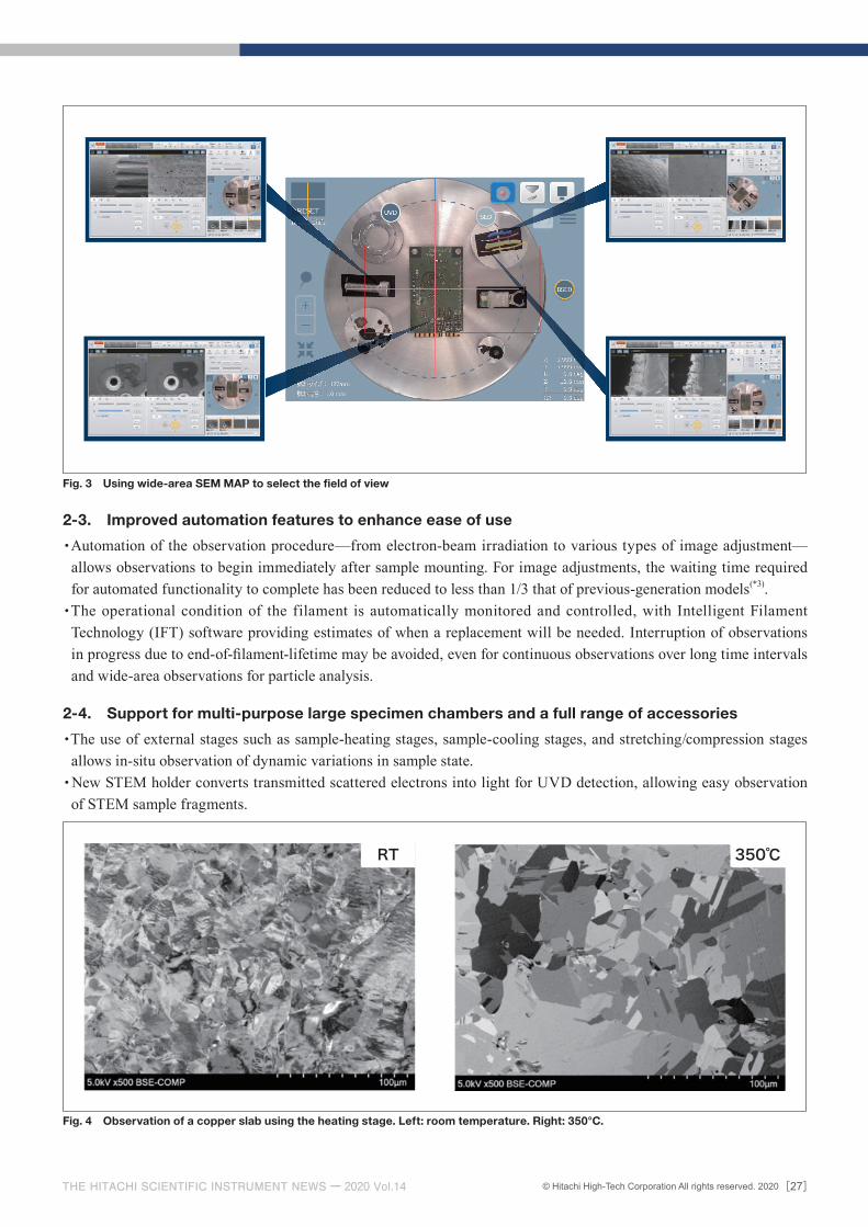
Fig. 3 Using wide-area SEM MAP to select the field of view
Fig. 4 Observation of a copper slab using the heating stage. Left: room temperature. Right: 350°C.
・Automation of the observation procedure—from electron-beam irradiation to various types of image adjustment—allows observations to begin immediately after sample mounting. For image adjustments, the waiting time required for automated functionality to complete has been reduced to less than 1/3 that of previous-generation models(*3).・The operational condition of the filament is automatically monitored and controlled, with Intelligent Filament
Technology (IFT) software providing estimates of when a replacement will be needed. Interruption of observations in progress due to end-of-filament-lifetime may be avoided, even for continuous observations over long time intervals and wide-area observations for particle analysis.
・The use of external stages such as sample-heating stages, sample-cooling stages, and stretching/compression stages allows in-situ observation of dynamic variations in sample state.・New STEM holder converts transmitted scattered electrons into light for UVD detection, allowing easy observation
of STEM sample fragments.
2-3. Improved automation features to enhance ease of use
2-4. Support for multi-purpose large specimen chambers and a full range of accessories
RT 350℃

© Hitachi High-Tech Corporation All rights reserved. 2020[28]THE HITACHI SCIENTIFIC INSTRUMENT NEWS ー 2020 Vol.14
Key Specifications3.
(*1)Identical to the S-3700N, Hitachi’s previous-generation large-scale SEM.(* 2)As compared to the S-3700N previous-generation model. The comparison involves only weight limitations for
in-plane motion of the sample stage.(* 3)As compared to the S-3700N previous-generation model.
Fig. 5 Observation of carbon nanotubes using the new STEM holder. Left: Bright-field STEM image. Right: Backscattered-electron image.
Item
Secondary-electron image resolution
Backscattered-electron image resolution
Accelerating voltage
Magnification
Sample stage
Maximum mountable sample size
Maximum observable range
Maximum sample thickness
Maximum sample weight
SU3800
3.0 nm (Accelerating voltage 30 kV, high-vacuum mode)15.0 nm (Accelerating voltage 1 kV, high-vacuum mode)
×5-×300,000 (photograph magnification),×7-×800,000 (true display magnification)
X: 0-100 mm, Y: 0-50 mm, Z: 5-65 mm, T: −20°-90°, R: 360°
X: 0-150 mm, Y: 0-150 mm, Z: 5-85 mm, T: −20°-90°, R: 360°
4.0 nm (Accelerating voltage 30 kV, low-vacuum mode)
0.3-30 kV
200 mm diameter 300 mm diameter
130 mm diameter (used with R) 200 mm diameter (used with R)
80 mm (WD=10 mm) 130 mm (WD=10 mm)
2 kg 5 kg (without T/R)
SU3900
About the author
Masanari FurikiMetrology and Analysis Systems DivisionNano-Technology Solution Business GroupHitachi High-Tech Corporation


![SI NEWS Vol · 2021. 3. 26. · THE HITACHI SCIENTIFIC INSTRUMENT NEWS 2020 Vol.14 ー © Hitachi High-Tech Corporation All rights reserved. 2020[28] 3. Key Specifications (*1)Identical](https://static.fdocuments.in/doc/165x107/614136c083382e045471f0e6/si-news-vol-2021-3-26-the-hitachi-scientific-instrument-news-2020-vol14-f.jpg)


![HITACHI CAPITAL CORPORATION HITACHI … the purposes of Directive 2004/39/EC ... HITACHI CAPITAL CORPORATION HITACHI CAPITAL (UK) PLC HITACHI CAPITAL AMERICA CORP. [[] [] ...](https://static.fdocuments.in/doc/165x107/5ad063b27f8b9a1d328e3da3/hitachi-capital-corporation-hitachi-the-purposes-of-directive-200439ec-.jpg)