ShockLine™ Compact Vector Network Analyzer … · MS46122A/B MM PN: 10410-00341 Rev. C 1-1...
48
Maintenance Manual ShockLine™ Compact Vector Network Analyzer MS46122A/B 1 MHz to 8 GHz 1 MHz to 20 GHz 1 MHz to 43.5 GHz MS46122A/B 43.5 GHz ShockLine VNA Part Number: 10410-00341 Revision: C Published: November 2017 Copyright 2017 Anritsu Company Anritsu Company 490 Jarvis Drive Morgan Hill, CA 95037-2809 USA http://www.anritsu.com
Transcript of ShockLine™ Compact Vector Network Analyzer … · MS46122A/B MM PN: 10410-00341 Rev. C 1-1...

Maintenance Manual
ShockLine™ CompactVector Network AnalyzerMS46122A/B
1 MHz to 8 GHz1 MHz to 20 GHz1 MHz to 43.5 GHz
MS46122A/B 43.5 GHz ShockLine VNA
Part Number: 10410-00341Revision: C
Published: November 2017Copyright 2017 Anritsu Company
Anritsu Company490 Jarvis DriveMorgan Hill, CA 95037-2809USAhttp://www.anritsu.com

MS46122A MM PN: 10410-00341 Rev. C Contents-1
Table of Contents
Chapter 1—General Information
1-1 Introduction. . . . . . . . . . . . . . . . . . . . . . . . . . . . . . . . . . . . . . . . . . . . . . . . . . . . . . . . . . . . . . . . 1-1
1-2 Description . . . . . . . . . . . . . . . . . . . . . . . . . . . . . . . . . . . . . . . . . . . . . . . . . . . . . . . . . . . . . . . . 1-1
Standard Accessories . . . . . . . . . . . . . . . . . . . . . . . . . . . . . . . . . . . . . . . . . . . . . . . . . . . . . 1-1
Available Options. . . . . . . . . . . . . . . . . . . . . . . . . . . . . . . . . . . . . . . . . . . . . . . . . . . . . . . . . 1-1
Identification Number. . . . . . . . . . . . . . . . . . . . . . . . . . . . . . . . . . . . . . . . . . . . . . . . . . . . . . 1-1
1-3 Related Documents . . . . . . . . . . . . . . . . . . . . . . . . . . . . . . . . . . . . . . . . . . . . . . . . . . . . . . . . . 1-2
1-4 Basic Maintenance . . . . . . . . . . . . . . . . . . . . . . . . . . . . . . . . . . . . . . . . . . . . . . . . . . . . . . . . . . 1-2
Calibration/Certification . . . . . . . . . . . . . . . . . . . . . . . . . . . . . . . . . . . . . . . . . . . . . . . . . . . . 1-2
Repair Service . . . . . . . . . . . . . . . . . . . . . . . . . . . . . . . . . . . . . . . . . . . . . . . . . . . . . . . . . . . 1-2
1-5 Anritsu Customer Service Centers . . . . . . . . . . . . . . . . . . . . . . . . . . . . . . . . . . . . . . . . . . . . . . 1-2
1-6 Recommended Test Equipment . . . . . . . . . . . . . . . . . . . . . . . . . . . . . . . . . . . . . . . . . . . . . . . . 1-3
1-7 Replaceable Parts and Assemblies . . . . . . . . . . . . . . . . . . . . . . . . . . . . . . . . . . . . . . . . . . . . . 1-4
Chapter 2— Performance Verification
2-1 Introduction to Performance Verification. . . . . . . . . . . . . . . . . . . . . . . . . . . . . . . . . . . . . . . . . . 2-1
2-2 VNA Traceability and Uncertainty. . . . . . . . . . . . . . . . . . . . . . . . . . . . . . . . . . . . . . . . . . . . . . . 2-1
First Tier of Uncertainty The VNA Calibration . . . . . . . . . . . . . . . . . . . . . . . . . . . . . . . . . 2-1
Second Tier of Uncertainty Systematic Measurement Errors. . . . . . . . . . . . . . . . . . . . . . 2-1
Third Tier of Uncertainty Random Measurement Error . . . . . . . . . . . . . . . . . . . . . . . . . . 2-2
Standards and Verification . . . . . . . . . . . . . . . . . . . . . . . . . . . . . . . . . . . . . . . . . . . . . . . . . 2-2
2-3 Process for Creation and Use of a Verification Kit . . . . . . . . . . . . . . . . . . . . . . . . . . . . . . . . . . 2-2
2-4 Electrostatic Discharge Prevention. . . . . . . . . . . . . . . . . . . . . . . . . . . . . . . . . . . . . . . . . . . . . . 2-3
2-5 Calibration and Measurement Conditions. . . . . . . . . . . . . . . . . . . . . . . . . . . . . . . . . . . . . . . . . 2-3
2-6 System Verification. . . . . . . . . . . . . . . . . . . . . . . . . . . . . . . . . . . . . . . . . . . . . . . . . . . . . . . . . . 2-4
Verification Result Determination . . . . . . . . . . . . . . . . . . . . . . . . . . . . . . . . . . . . . . . . . . . . 2-5
2-7 System Verification Procedure . . . . . . . . . . . . . . . . . . . . . . . . . . . . . . . . . . . . . . . . . . . . . . . . . 2-6
Equipment Required . . . . . . . . . . . . . . . . . . . . . . . . . . . . . . . . . . . . . . . . . . . . . . . . . . . . . . 2-6
Special Precautions. . . . . . . . . . . . . . . . . . . . . . . . . . . . . . . . . . . . . . . . . . . . . . . . . . . . . . . 2-6
MS46122A Verification Procedure . . . . . . . . . . . . . . . . . . . . . . . . . . . . . . . . . . . . . . . . . . . 2-6
MS46122B Verification Procedure . . . . . . . . . . . . . . . . . . . . . . . . . . . . . . . . . . . . . . . . . . . 2-8
If Verification Fails . . . . . . . . . . . . . . . . . . . . . . . . . . . . . . . . . . . . . . . . . . . . . . . . . . . . . . . . 2-9
Chapter 3—Adjustment
3-1 Introduction. . . . . . . . . . . . . . . . . . . . . . . . . . . . . . . . . . . . . . . . . . . . . . . . . . . . . . . . . . . . . . . . 3-1
3-2 Source Level Adjustment Procedure . . . . . . . . . . . . . . . . . . . . . . . . . . . . . . . . . . . . . . . . . . . . 3-1
Equipment Required . . . . . . . . . . . . . . . . . . . . . . . . . . . . . . . . . . . . . . . . . . . . . . . . . . . . . . 3-1
Procedure . . . . . . . . . . . . . . . . . . . . . . . . . . . . . . . . . . . . . . . . . . . . . . . . . . . . . . . . . . . . . . 3-1
3-3 IF Adjustment Procedure . . . . . . . . . . . . . . . . . . . . . . . . . . . . . . . . . . . . . . . . . . . . . . . . . . . . . 3-4
Equipment Required . . . . . . . . . . . . . . . . . . . . . . . . . . . . . . . . . . . . . . . . . . . . . . . . . . . . . . 3-4
Procedure . . . . . . . . . . . . . . . . . . . . . . . . . . . . . . . . . . . . . . . . . . . . . . . . . . . . . . . . . . . . . . 3-4
Contents-2 PN: 10410-00341 Rev. C MS46122A MM
3-4 Time Base Adjustment Procedure . . . . . . . . . . . . . . . . . . . . . . . . . . . . . . . . . . . . . . . . . . . . . . 3-5
Equipment Required . . . . . . . . . . . . . . . . . . . . . . . . . . . . . . . . . . . . . . . . . . . . . . . . . . . . . . 3-5
Procedure . . . . . . . . . . . . . . . . . . . . . . . . . . . . . . . . . . . . . . . . . . . . . . . . . . . . . . . . . . . . . . 3-5
Chapter 4—Troubleshooting
4-1 Introduction . . . . . . . . . . . . . . . . . . . . . . . . . . . . . . . . . . . . . . . . . . . . . . . . . . . . . . . . . . . . . . . . 4-1
4-2 General Safety Warnings . . . . . . . . . . . . . . . . . . . . . . . . . . . . . . . . . . . . . . . . . . . . . . . . . . . . . 4-1
4-3 Troubleshooting Test – Non-Ratio Power Level Check . . . . . . . . . . . . . . . . . . . . . . . . . . . . . . 4-2
Equipment Required . . . . . . . . . . . . . . . . . . . . . . . . . . . . . . . . . . . . . . . . . . . . . . . . . . . . . . 4-2
Procedure . . . . . . . . . . . . . . . . . . . . . . . . . . . . . . . . . . . . . . . . . . . . . . . . . . . . . . . . . . . . . . 4-2
4-4 Troubleshooting Turn-on Problems . . . . . . . . . . . . . . . . . . . . . . . . . . . . . . . . . . . . . . . . . . . . . 4-3
Unit Cannot Power Up . . . . . . . . . . . . . . . . . . . . . . . . . . . . . . . . . . . . . . . . . . . . . . . . . . . . . 4-3
ShockLine Application Cannot Launch . . . . . . . . . . . . . . . . . . . . . . . . . . . . . . . . . . . . . . . . 4-3
4-5 Troubleshooting Operating Problems . . . . . . . . . . . . . . . . . . . . . . . . . . . . . . . . . . . . . . . . . . . . 4-3
Frequency Related Problems . . . . . . . . . . . . . . . . . . . . . . . . . . . . . . . . . . . . . . . . . . . . . . . 4-3
RF Power Related Problems . . . . . . . . . . . . . . . . . . . . . . . . . . . . . . . . . . . . . . . . . . . . . . . . 4-3
4-6 Troubleshooting Measurement Problems. . . . . . . . . . . . . . . . . . . . . . . . . . . . . . . . . . . . . . . . . 4-4
VNA Measurement Quality . . . . . . . . . . . . . . . . . . . . . . . . . . . . . . . . . . . . . . . . . . . . . . . . . 4-4
Checking Possible Measurement Problems . . . . . . . . . . . . . . . . . . . . . . . . . . . . . . . . . . . . 4-4
Chapter 5—Assembly Removal and Replacement
5-1 Introduction . . . . . . . . . . . . . . . . . . . . . . . . . . . . . . . . . . . . . . . . . . . . . . . . . . . . . . . . . . . . . . . . 5-1
5-2 Electrostatic Discharge Prevention . . . . . . . . . . . . . . . . . . . . . . . . . . . . . . . . . . . . . . . . . . . . . 5-1
5-3 Instrument Enclosure Overview . . . . . . . . . . . . . . . . . . . . . . . . . . . . . . . . . . . . . . . . . . . . . . . . 5-1
5-4 Disassembly Procedure . . . . . . . . . . . . . . . . . . . . . . . . . . . . . . . . . . . . . . . . . . . . . . . . . . . . . . 5-3
Common Disassembly Procedure . . . . . . . . . . . . . . . . . . . . . . . . . . . . . . . . . . . . . . . . . . . . 5-3
5-5 VNA Assembly and Adapter Board Assembly . . . . . . . . . . . . . . . . . . . . . . . . . . . . . . . . . . . . . 5-5
Replacement Parts . . . . . . . . . . . . . . . . . . . . . . . . . . . . . . . . . . . . . . . . . . . . . . . . . . . . . . . 5-5
Reference Figures . . . . . . . . . . . . . . . . . . . . . . . . . . . . . . . . . . . . . . . . . . . . . . . . . . . . . . . . 5-5
Replacement Procedure . . . . . . . . . . . . . . . . . . . . . . . . . . . . . . . . . . . . . . . . . . . . . . . . . . . 5-8
5-6 Front Panel LED PCB Assembly . . . . . . . . . . . . . . . . . . . . . . . . . . . . . . . . . . . . . . . . . . . . . . . 5-9
Replacement Part . . . . . . . . . . . . . . . . . . . . . . . . . . . . . . . . . . . . . . . . . . . . . . . . . . . . . . . . 5-9
Reference Figure . . . . . . . . . . . . . . . . . . . . . . . . . . . . . . . . . . . . . . . . . . . . . . . . . . . . . . . . . 5-9
Replacement Procedure . . . . . . . . . . . . . . . . . . . . . . . . . . . . . . . . . . . . . . . . . . . . . . . . . . 5-10
5-7 Test Port Adapter . . . . . . . . . . . . . . . . . . . . . . . . . . . . . . . . . . . . . . . . . . . . . . . . . . . . . . . . . . 5-11
Replacement Part . . . . . . . . . . . . . . . . . . . . . . . . . . . . . . . . . . . . . . . . . . . . . . . . . . . . . . . 5-11
Reference Figures . . . . . . . . . . . . . . . . . . . . . . . . . . . . . . . . . . . . . . . . . . . . . . . . . . . . . . . 5-11
Replacement Procedure . . . . . . . . . . . . . . . . . . . . . . . . . . . . . . . . . . . . . . . . . . . . . . . . . . 5-14
Appendix A—Test Records
A-1 Introduction . . . . . . . . . . . . . . . . . . . . . . . . . . . . . . . . . . . . . . . . . . . . . . . . . . . . . . . . . . . . . . . . A-1
A-2 ShockLine MS46122A/B Test Record . . . . . . . . . . . . . . . . . . . . . . . . . . . . . . . . . . . . . . . . . . . A-2
System Performance Verification . . . . . . . . . . . . . . . . . . . . . . . . . . . . . . . . . . . . . . . . . . . . A-2
Index

MS46122A/B MM PN: 10410-00341 Rev. C 1-1
Chapter 1 — General Information
1-1 IntroductionThis manual provides service and maintenance information for the Anritsu ShockLine MS46122A/B Vector Network Analyzer. The information includes a product description, performance verification procedures, parts removal and replacement procedures, and troubleshooting information.
1-2 Description The ShockLine MS46122A/B Vector Network Analyzer is a very low-cost series of 1U high, 2-port Compact Vector Network Analyzer. It is based on patented ShockLine VNA-on-chip technology, which simplifies the internal VNA architecture at high frequencies, reduces instrument cost, and enhances accuracy and measurement repeatability. The combination of low cost and good performance make the MS46122AB Vector Network Analyzer an ideal candidate for testing RF and Microwave passive devices to 43.5 GHz. The MS46122AB Vector Network Analyzer is controlled through USB from an external PC.
Standard Accessories
Each instrument includes:
• A user documentation/software USB device that includes:
• ShockLine application software for controlling the VNA.
• Portable document format (PDF) files of the MS46122A/B Operation Manual and Technical Data Sheet
• Power Cord
• AC/DC Adapter
• USB 2.0 A to Mini B Cable
• Rack Mount Kit for shelf-mounting into a 19 inch universal rack
Available Options
The main system options are:
• MS46122A-002/ MS46122B-002 Time Domain
• MS46122A-010/ MS46122B-010 Frequency Option, 1 MHz to 8 GHz, type N(f) test ports
• MS46122A-020/ MS46122B-020 Frequency Option, 1 MHz to 20 GHz, type K(m) test ports
• MS46122A-040/ MS46122B-040 Frequency Option, 1 MHz to 43.5 GHz, type K(m) test ports
Identification Number
All Anritsu MS46122A/B instruments are assigned a seven-digit ID number (Serial Number), such as “1334003”. This number appears on a decal affixed to the rear panel.
When corresponding with Anritsu Customer Service, please use this identification number with reference to the specific instrument model number, installed options, and serial number. For example, an MS46122A/B, Option 2, Option 10, Serial Number 1234567.

1-3 Related Documents General Information
1-2 PN: 10410-00341 Rev. C MS46122A/B MM
1-3 Related Documents Other documents are available for theMS46122A/B at the Anritsu web site at: www.anritsu.com
• ShockLine MS46122A/B Series VNA Technical Data Sheet – part number 11410-00822
• ShockLine MS46122A/B VNA Operation Manual – part number 10410-00340
• ShockLine MS46122A/B VNA User Interface Reference – part number 10410-00337
• ShockLine MS46122A/B VNA Measurement Guide – part number 10410-00336
• ShockLine MS46122A/B VNA Programming Manual – part number 10410-00338
• ShockLine Product Information, Compliance, and Safety – 10100-00067
1-4 Basic Maintenance
Calibration/Certification
Test instruments are often put on a calibration cycle for performance verification in order to provide quality assurance. The details of the performance verification procedures are included in Chapter 2 — Performance Verification.
Repair Service
In the event that the MS46122A/B VNA requires repair, contact your local Anritsu Service Center. See Section 1-5 “Anritsu Customer Service Centers” for contact information. When contacting an Anritsu Service Center, please provide the following information:
• Your company name and address
• The model number and serial number of the instrument
• A detailed description of the problem
1-5 Anritsu Customer Service CentersFor the latest service and sales information in your area, please visit the following URL:
http://www.anritsu.com/contact.asp
Choose a country for regional contact information.

General Information 1-6 Recommended Test Equipment
MS46122A/B MM PN: 10410-00341 Rev. C 1-3
1-6 Recommended Test Equipment The following test equipment is recommended for use in testing and maintaining the ShockLine MS46122A/B.
Table 1-1. Recommended Test Equipment
Equipment Critical SpecificationRecommended Manufacturer/Model
Use Codesa
a. P= Performance Verification; A = Adjustment
Calibration Tee (For Opt. 10) Frequency: DC to 8 GHz Connector: N(m)
Anritsu Model OSLN50A-8 or TOSLN50A-8
P
Calibration Tee (For Opt. 10) Frequency: DC to 8 GHz Connector: N(f)
Anritsu Model OSLNF50A-8 or TOSLNF50A-8
P
Verification Kit (For MS46122A Opt. 10)
Connector: N TypeAnritsu Model 3663-2 (Includes Verification Software)
P
Verification Kit (For MS46122B Opt. 10)
Connector: N TypeAnritsu Model 3663-3 (Includes Verification Software)
P
Torque Wrench (For Opt. 10)3/4 in Open End Wrench 12 lbf·in (1.35 N·m)
Anritsu Model 01-200 P
AdapterFrequency: DC to 18 GHz Connector: N(m) to K(m)
Anritsu Model 34NK50 P, A
AdapterFrequency: DC to 18 GHz Connector: N(m) to K(f)
Anritsu Model 34NKF50 P, A
RF Coaxial CableFrequency: DC to 40 GHz Impedance: 50 ohm Connector: K(f) to K(m)
Anritsu Model 3670K50-2 P, A
Calibration Tee (For Opt. 20 and 40)
Frequency: DC to 40 GHz Connector: K(m)
Anritsu Model TOSLK50A-40 P
Calibration Tee (For Opt. 20 or 40)
Frequency: DC to 40 GHz Connector: K(f)
Anritsu Model TOSLKF50A-40 P
Verification Kit (For MS46122A Opt. 20 or 40)
Connector: K TypeAnritsu Model 3668-2 (Includes Verification Software)
P
Verification Kit (For MS46122B Opt. 20 or 40)
Connector: K TypeAnritsu Model 3668-3 (Includes Verification Software)
P
Adapter (For Opt. 20 or 40) Connector: K(m) to K(f) Anritsu Model 33KKF50B P
Adapter (For Opt. 20 or 40) Connector: K(f) to K(f) Anritsu Model 33KFKF50B P
Torque Wrench (For Opt. 20 or 40)
5/16 in Open End Wrench 8 lbf·in (0.325 N·m)
Anritsu Model 01-201 P
Personal Computer
Operating System: Windows 7 Interface: USB 2.0 ASoftware: National Instruments VISA version 4.4.1 or later
Any P
Power Sensor (For Opt. 10)Frequency: 10 MHz to 18 GHz Connector Type: N(m)
Anritsu Model MA24118A A
Power Sensor (For Opt. 20 or 40)Frequency: 10 MHz to 40 GHz Connector Type: K(m)
Anritsu Model SC8268 A
Frequency Counter Frequency: 5 GHzAnritsu Model MF2412C with Option 3
A

1-7 Replaceable Parts and Assemblies General Information
1-4 PN: 10410-00341 Rev. C MS46122A/B MM
1-7 Replaceable Parts and AssembliesTo ensure that the correct options are provided on the replacement assembly when ordering a VNA Module Assembly, all installed instrument options must be declared on the order.
The installed options are listed on a label on the rear panel of the MS46122AB. They can also be viewed in the ShockLine application About box display (Select 9 Help | 1. About Anritsu).
The tables below summarize the available replaceable parts and assemblies.
Table 1-2. MS46122A Replaceable Parts and Assemblies
Part Number Description
ND81301<R> VNA Assembly of MS46122A instruments with Option 10
ND81302<R> VNA Assembly of MS46122A instruments with Option 20
ND81303<R> VNA Assembly of MS46122A instruments with Option 40
ND81018 Front Panel LED PCB Assembly
3-80719-3 Adapter Board Assembly
40-187-R AC/DC Adapter
3-2000-1498 USB 2.0 A to Mini B Cable, 10 ft
3-75651 Ruggedized K male Test Port Adapter
3-513-122 N female Test Port Adapter
Table 1-3. MS46122B Replaceable Parts and Assemblies
Part Number Description
3-ND83417<R> VNA Assembly of MS46122B instruments with Option 10
3-ND83418<R> VNA Assembly of MS46122B instruments with Option 20
3-ND83419<R> VNA Assembly of MS46122B instruments with Option 40
3-ND81018 Front Panel LED PCB Assembly
3-80719-3 Adapter Board Assembly
40-187-R AC/DC Adapter
3-2000-1498 USB 2.0 A to Mini B Cable, 10 ft
3-75651 Ruggedized K male Test Port Adapter
3-82848 N female Test Port Adapter

MS46122A MM PN: 10410-00341 Rev. C 2-1
Chapter 2 — Performance Verification
2-1 Introduction to Performance VerificationThis chapter provides procedures to be used to verify the performance of the ShockLineMS46122A. There are many levels to the concept of VNA “verification” which ultimately is a comparison against expected behaviors.
On the explicit VNA hardware level are operational checkout items such as port power and noise levels. On the calibrated instrument level (which includes the VNA and the calibration kit or AutoCal automatic calibration module) are the residual specifications (corrected directivity, source match, load match, and tracking), which are measured using traceable airlines (absolute impedance standards).
The intermediate level looks at overall system behavior (VNA, calibration kit, cables, environment) in a traceable fashion through the use of a verification kit. While not intended for day-to-day use, the verification kit provides a periodic check of system behavior without going through the rigor needed for full residual analysis (which can usually be done less often).
While there are many ways of verifying VNA performance, sometimes simple procedures are desired. The use of a verification kit, available from Anritsu, is a simple method of verifying the measurement capabilities of the instrument by analyzing the measurement of artifacts that are traceable to national standards laboratories.
2-2 VNA Traceability and UncertaintyVector network analyzers (VNAs) are precision instruments for making high frequency and broadband measurements in devices, components, and instrumentations. The accuracy of these measurements is affirmed by demonstrated and adequate traceability of measurement standards. Metrological traceability, per International vocabulary of metrology, JCGM 200:2008, is property of a measurement result whereby the result can be related to a reference through a documented unbroken chain of calibrations, each contributing to the measurement uncertainty. For the accuracy of VNAs and quality assurance by users, two standard approaches were created to ensure sound metrology traceability. One is to construct tight uncertainty budget and specifications in three tiers from the ground up, and the other is to develop a calibration hierarchy for systematic verification. The three-tier process is depicted in the sections below.
First Tier of Uncertainty The VNA Calibration
A traceable VNA itself requires proper calibration for several key quantities; for example frequency, power level, and high level noise via traceable standards to the SI units. Each contributing uncertainty was evaluated at the time of instrument calibration.
The inception of a precision VNA is accuracy-enhanced 50 ohm impedance, which is characterized in lieu of coaxial transmission lines all with proper propagation properties throughout the whole measurement systems including the device-under-test. A transmission line for VNAs is best represented by a coaxial airline, which was precisely selected and machined based on the electromagnetic properties of conductivity and skin depth, etc. Therefore, the dimensional measurement accuracy of the airline gives out the first tier of measurement uncertainty of impedance quantity.
Second Tier of Uncertainty Systematic Measurement Errors
The second tier of uncertainty, corrected or residual uncertainty, is the result of the accuracy enhancement of VNA calibration to remove systematic errors. Systematic measurement errors are components of measurement error that in replicate measurements remains constant or values in a predictable manner. This accuracy enhancement is usually the function of calibration kits. The choice of calibration kits used dictates the level of uncertainties for the intended measurements or applications.
2-3 Process for Creation and Use of a Verification Kit Performance Verification
2-2 PN: 10410-00341 Rev. C MS46122A MM
Third Tier of Uncertainty Random Measurement Error
The third tier of uncertainty is random measurement error that in replicate measurements varies in an unpredictable manner. The examples are connector repeatability and cable stability, etc. Random measurement error equals measurement error minus systematic measurement error.
Standards and Verification
Most often, instrument end users demand system verifications in order to provide quality assurance. This is accomplished by utilizing a set of known or characterized devices; for example verification kits for comparison. It can also be done by using devices that are different from the calibration kit. The calibration hierarchy of verification uncertainty is built through unbroken chain comparisons with the national standards.
• Physical standards airline dimensionality impedance standard residuals and port parameters
• Basic power standards power sensors power accuracy specifications
• Basic time standards frequency reference source frequency accuracy
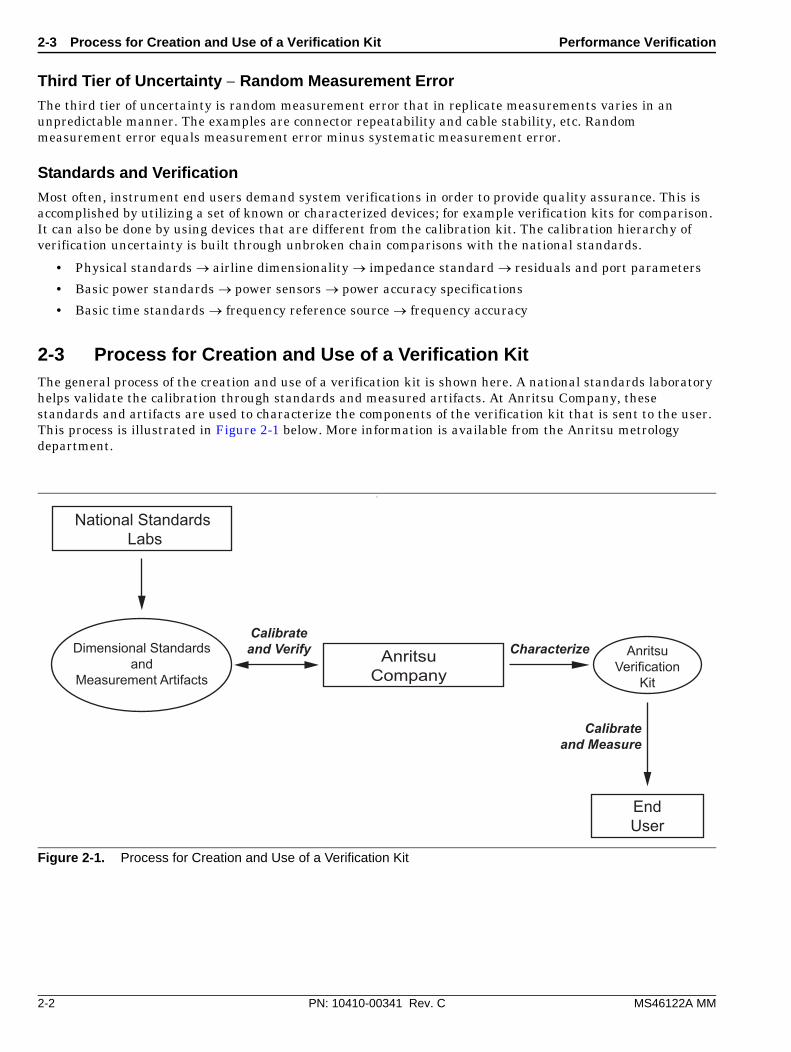
2-3 Process for Creation and Use of a Verification KitThe general process of the creation and use of a verification kit is shown here. A national standards laboratory helps validate the calibration through standards and measured artifacts. At Anritsu Company, these standards and artifacts are used to characterize the components of the verification kit that is sent to the user. This process is illustrated in Figure 2-1 below. More information is available from the Anritsu metrology department.
f
Figure 2-1. Process for Creation and Use of a Verification Kit
National Standards Labs
Dimensional Standardsand
Measurement Artifacts
AnritsuCompany
AnritsuVerification
Kit
CharacterizeCalibrateand Verify
Calibrateand Measure
EndUser
Performance Verification 2-4 Electrostatic Discharge Prevention
MS46122A MM PN: 10410-00341 Rev. C 2-3
2-4 Electrostatic Discharge PreventionAll electronic devices, components, and instruments can be damaged by electrostatic discharge. Thus, it is important to take preventative measures to protect the instrument from damage caused by electrostatic discharge. Prior to connecting a test port cable to the VNA test port, take steps to eliminate the static charges built-up on the test port cable. This can be done by terminating the open-end of the cable with the short from the calibration kit and then grounding the outer conductor of the connector on the cable.
2-5 Calibration and Measurement ConditionsExtremes in the surrounding environmental conditions and the condition and stability of the test port connectors, through cable, and calibration kit determine system measurement integrity to a large extent. These are all user controlled conditions, and as such, should be evaluated periodically for impact on system performance. If these conditions vary significantly with time, the system verification procedures should be performed more often than the recommended annual cycle.
The standard conditions specified below must be observed when performing any of the operations in this chapter – both during calibration and during measurement.
• Warm-up Time:
• 45 minutes
• Environmental Conditions
• Temperature
• For system verification, 23 °C ± 3 °C, with < 1 °C variation from calibration temperature
• For other tests, 25 °C ± 5 °C
• Relative Humidity
• 20 % to 50 % recommended
2-6 System Verification Performance Verification
2-4 PN: 10410-00341 Rev. C MS46122A MM
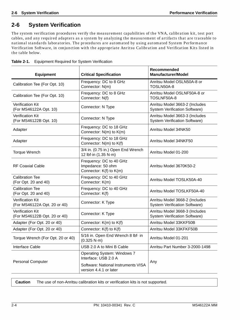
2-6 System VerificationThe system verification procedures verify the measurement capabilities of the VNA, calibration kit, test port cables, and any required adapters as a system by analyzing the measurement of artifacts that are traceable to national standards laboratories. The procedures are automated by using automated System Performance Verification Software, in conjunction with the appropriate Anritsu Calibration and Verification Kits listed in the table below.
Table 2-1. Equipment Required for System Verification
Equipment Critical SpecificationRecommended Manufacturer/Model
Calibration Tee (For Opt. 10)Frequency: DC to 8 GHz Connector: N(m)
Anritsu Model OSLN50A-8 or TOSLN50A-8
Calibration Tee (For Opt. 10)Frequency: DC to 8 GHz Connector: N(f)
Anritsu Model OSLNF50A-8 or TOSLNF50A-8
Verification Kit (For MS46122A Opt. 10)
Connector: N TypeAnritsu Model 3663-2 (Includes System Verification Software)
Verification Kit (For MS46122B Opt. 10)
Connector: N TypeAnritsu Model 3663-3 (Includes System Verification Software)
AdapterFrequency: DC to 18 GHz Connector: N(m) to K(m)
Anritsu Model 34NK50
AdapterFrequency: DC to 18 GHz Connector: N(m) to K(f)
Anritsu Model 34NKF50
Torque Wrench3/4 in. (0.75 in.) Open End Wrench 12 lbf·in (1.35 N·m)
Anritsu Model 01-200
RF Coaxial CableFrequency: DC to 40 GHz Impedance: 50 ohm Connector: K(f) to K(m)
Anritsu Model 3670K50-2
Calibration Tee (For Opt. 20 and 40)
Frequency: DC to 40 GHz Connector: K(m)
Anritsu Model TOSLK50A-40
Calibration Tee (For Opt. 20 and 40)
Frequency: DC to 40 GHz Connector: K(f)
Anritsu Model TOSLKF50A-40
Verification Kit (For MS46122A Opt. 20 or 40)
Connector: K TypeAnritsu Model 3668-2 (Includes System Verification Software)
Verification Kit (For MS46122B Opt. 20 or 40)
Connector: K TypeAnritsu Model 3668-3 (Includes System Verification Software)
Adapter (For Opt. 20 or 40) Connector: K(m) to K(f) Anritsu Model 33KKF50B
Adapter (For Opt. 20 or 40) Connector: K(f) to K(f) Anritsu Model 33KFKF50B
Torque Wrench (For Opt. 20 or 40)5/16 in. Open End Wrench 8 lbf· in (0.325 N·m)
Anritsu Model 01-201
Interface Cable USB 2.0 A to Mini B Cable Anritsu Part Number 3-2000-1498
Personal Computer
Operating System: Windows 7 Interface: USB 2.0 A
Software: National Instruments VISA version 4.4.1 or later
Any
Caution The use of non-Anritsu calibration kits or verification kits is not supported.
Performance Verification 2-6 System Verification
MS46122A MM PN: 10410-00341 Rev. C 2-5
The System Performance Verification Software guides the user to perform a full 12 Term calibration on the VNA using the appropriate calibration kit, measure the S-parameters of the impedance transfer standards in the verification kit, and to verify that the measured values are within the specified measurement uncertainty limits.
The impedance transfer standards contained in the verification kit are:
• 20 dB Attenuation Standard
• 50 dB Attenuation Standard
• 50 ohm Air Line Standard
• 25 ohm Mismatch (Beatty) Standard
The devices in the verification kit are selected based on their ability to stress the envelope of possible measurement parameters while still providing a very stable and repeatable behavior. The key attribute of the devices is that of long term stability.
Pass/Fail status of the measurements is displayed on the computer. The software can also provide hardcopy (printout) of the test reports which include the measured data, the measurement uncertainties, and the Pass/Fail status.
Verification Result Determination
The software verification process compares the measured S-parameter data of the impedance transfer standards against the original standard (characterization) data for those devices that was obtained using the factory standard vector network analyzer (at Anritsu). The factory standard vector network analyzer system is traceable to NIST through the impedance standards of the Anritsu calibration laboratory. These standards are traceable to NIST through precision mechanical measurements, NIST-approved microwave theory impedance derivation methods, and electrical impedance comparison measurements.
At each frequency point, the verification measurement is compared to the characterization measurement in the context of the uncertainties. If the delta between the two measurements is consistent with the uncertainty window, the measurement is considered acceptable at that point. The metric of comparison, termed En, is a check to see if the measurement differences are consistent with the uncertainty windows of both the characterization and the verification measurements. The quantity is shown in the formula below:
where:
• The numerator contains the magnitude or phase of S-parameters measured during characterization (by Anritsu) and during verification (by the user).
• The denominator contains the respective uncertainties.
These uncertainties are calculated based on the VNA, the calibration kit, and repeatability. If this quantity En is less than 1, then the measurements during the two phases are within the overlap of the uncertainties and one can consider the measurements “equivalent” and, in some sense, verified.
En
Xxychar
Xxyver
–
Uxychar
2Uxy
ver 2
+
------------------------------------------------------------=

2-7 System Verification Procedure Performance Verification
2-6 PN: 10410-00341 Rev. C MS46122A MM
The quality of the verification results is very dependent on the degree of care taken by the user in maintaining, calibrating, and using the system. The most critical factors are:
• The stability and quality of the devices in the calibration kit and verification kit.
• The condition of the VNA test port connectors and test port cables.
• The pin depths of all connectors and the proper torquing of connections. These same factors also affect the VNA measurement quality.
Consult the reference manual supplied with Anritsu Calibration Kits and Verification Kits for proper use, care, and maintenance of the devices contained in these kits.
2-7 System Verification ProcedureThe system verification procedure is described below. The procedure assumes that the system verification software has been installed to an external personal computer running Microsoft Windows operating system and the National Instruments VISA runtime.
Equipment Required
• Personal Computer:
• With Microsoft Windows operating system
• With National Instruments VISA runtime
• USB 2.0 A to Mini B cable
• Anritsu Calibration Tees (Refer to Table 2-1, “Equipment Required for System Verification” on page 2-4)
• Anritsu Verification Kit (Refer to Table 2-1)
• Anritsu Test Port Cables (Refer to Table 2-1)
Special Precautions
When performing the procedures, observe the following precautions:
• Minimize vibration and movement of the system, attached components, and test cables.
• Clean and check the pin depth and condition of all adapters, test port cables, calibration components, and impedance transfer standards.
• Pre-shape the test cables so as to minimize their movement during calibration and measurement activities.
MS46122A Verification Procedure
1. Turn on power to the PC controller.
2. Install the ShockLine Application software to the PC controller.
3. Install the MS46122A system verification software, which can be found on the USB memory stick supplied with the 366x-2 verification kit, to the PC controller.
4. 4.Connect a USB 2.0 A to Mini B cable between the Mini B port of the ShockLine MS46122A and the USB 2.0 A port of the PC controller. Refer to the MS46122A/B Operation Manual, PN 10410-00340, for setup procedures
5. Turn on the ShockLineMS46122A and allow the instrument to warm up for 45 minutes.
6. When verifying an MS46122A with Option 10:
a. Install the 34NK50 and 34NKF50 Adapters to the 3670K50-2 Through Cable. Use a torque wrench to tighten the K connectors to ensure that the connections do not become loose during the test.
b. Install the through cable with the adapter to Port 2 of the ShockLine MS46122A.

Performance Verification 2-7 System Verification Procedure
MS46122A MM PN: 10410-00341 Rev. C 2-7
7. When verifying an MS46122A with Option 20 or 40:
a. Install the 33KFKF50B adapter to Port 1 of the ShockLineMS46122A.
b. Install the through cable to Port 2 of the ShockLineMS46122A.
c. Install the 33KKF50B adapter on the open end of the through cable.
8. Run the ShockLineMS46122A verification software on the PC controller.
9. Click on the Begin VNA Verification button and then select TCP/IP.
10. Enter 127.0.0.1 to the IP Address text box in the TCP/IP section as shown in Figure 2-2.
11. Verify that the PC controller is communicating with the ShockLineMS46122A by clicking the Check VNA Connection button of the verification software.
12. Insert the USB flash drive that is supplied with the verification kit into an available USB port on the PC controller. Set the data location of the verification software to the USB flash drive when prompted.
13. Follow the directions that are displayed on the computer to perform the calibration with the four impedance transfer standards for the appropriate calibration kit.
CautionUse an appropriate torque wrench to insure proper connection of calibration devices during calibration.
Figure 2-2. TCP/IP IP Address

2-7 System Verification Procedure Performance Verification
2-8 PN: 10410-00341 Rev. C MS46122A MM
14. After all tests are complete, print the test results and attach the printouts to the test record in Appendix A, “ShockLine MS46122A/B Test Record”
MS46122B Verification Procedure
1. Turn on power to the PC controller.
2. Install the ShockLine Application software to the PC controller.
3. Install the MS46122B system verification software, which can be found on the USB memory stick supplied with the 366x-3 verification kit, to the PC controller. Refer to Section 5 of the ShockLine Series Vector Network Analyzers Verification Kits and Performance Verification Software Quick Start Guide, PN 10410-00766, for instructions.
4. Connect a USB 2.0 A to Mini B cable between the Mini B port of the ShockLine MS46122B and the USB 2.0 A port of the PC controller. Refer to Section 4 of the ShockLine Series Vector Network Analyzers Verification Kits and Performance Verification Software Quick Start Guide, PN 10410-00766, for instructions.
5. Turn on the ShockLine MS46122B and allow the instrument to warm up for 45 minutes.
6. When verifying an MS46122B with Option 10:
a. Install the 34NK50 and 34NKF50 Adapters to the 3670K50-2 Through Cable. Use a torque wrench to tighten the K connectors to ensure that the connections do not become loose during the test.
b. Install the through cable with the adapter to Port 2 of the ShockLine MS46122B.
Note
The user can run all the automated tests in a consecutive fashion or run individual test selectively. If all are selected, the test sequence is:
1. VNA Calibration
2. Airline (DAT) Measurements
3. Airline (UNC) Uncertainty Computation [Pass/Fail Determination]
4. Beatty Airline (DAT) Measurements
5. Beatty Airline (UNC) Uncertainty Computation
6. 20 dB Offset (Pad) (DAT) Measurements
7. 20 dB Offset (Pad) (UNC) Uncertainty Computation
8. 50 dB Offset (Pad) (DAT) Measurements
9. 50 dB Offset (Pad) (UNC) Uncertainty Computation
Note
Each test generates a data report file in TEXT (ASCII) file format. The data report files can be viewed and printed either using the software built-in “Print” function or other software applications, such as Notepad or other word processors. The data report files are:
• 20 DB OFFSET (UNC) #VER.TXT
• 50 DB OFFSET (UNC) #VER.TXT
• AIRLINE (UNC) #VER.TXT
• BEATTY (UNC) #VER.TXT
These files can be found in the following folder on the hard drive of the PC controller:
C:\Anritsu ShockLine Verification\VNA_Reports\MS46122A_xxxxxxx
[where xxxxxxx is the serial number of the ShockLine™ MS46122A being tested]

Performance Verification 2-7 System Verification Procedure
MS46122A MM PN: 10410-00341 Rev. C 2-9
7. When verifying an MS46122B with Option 20 or 40:
a. Install the 33KFKF50B adapter to Port 1 of the ShockLine MS46122B.
b. Install the through cable to Port 2 of the ShockLine MS46122B.
c. Install the 33KKF50B adapter on the open end of the through cable.
8. Run the MS46122B VNA verification software on the PC controller.
9. Insert the USB flash drive that is supplied with the 366x-3 verification kit to an available USB port on the PC controller. Follow the instructions in Section 6 of the ShockLine Series Vector Network Analyzers Verification Kits and Performance Verification Software Quick Start Guide, PN 10410-00766, to add the four impedance transfer standards to the verification tools database.
10. Follow the instructions in Section 6 of the Quick Start Guide to add the calibration kits to the verification tools database.
11. On the verification software graphic user interface (GUI) displayed on the PC controller, locate the Select Interface field and then select TCP/IP using the drop-down menu.
12. Enter the Local Host address 127.0.0.1::5001 into the Address field of the verification software GUI.
13. On the VNA, select: Main Menu | System | Network Interface.
14. Enter 127.0.0.1 to the IP Address.
15. Follow the instructions in Section 7 of the Quick Start Guide to start the performance verification testing.
16. After all tests are complete, print the test results and attach the printouts to the test record in Appendix A, “ShockLine MS46122A/B Test Record”
If Verification Fails
If the verification fails, then check the quality, cleanliness, and installation methods for the calibration and verification components. Specifically, check for the most common causes for verification failures:
• The VNA test port connectors
• The calibration tee
• The impedance transfer standards
• The test port cables, for damage and cleanliness
• The test port cables, for proper connection and torquing
• The test port cables, for phase stability
CautionUse an appropriate torque wrench to insure proper connection of calibration devices during calibration.
2-7 System Verification Procedure Performance Verification
2-10 PN: 10410-00341 Rev. C MS46122A MM
MS46122A MM PN: 10410-00341 Rev. C 3-1
Chapter 3 — Adjustment
3-1 IntroductionThis chapter contains procedures that are used to restore and optimize the operation of the MS46122A/B Vector Network Analyzer.
3-2 Source Level Adjustment ProcedureThis section provides the procedure to restore or optimize the operation of MS46122A/B related to the RF leveling at the VNA Test Ports.
Equipment Required
• Anritsu Model MA24118A USB Power Sensor (for units with N(f) test ports)
• Anritsu Model SC8268 USB Power Sensor (for units with K(m) test ports)
Procedure
1. On the PC controller, install the PowerXpert Analysis and Control software that is supplied with the USB power sensor. This will install the Windows driver needed to control the USB power sensor.
2. Power on the VNA and allow the instrument to warm up for at least 45 minutes.
3. Insert the USB power sensor interface cable into an open USB port on the PC controller. Wait for Windows to load the USB power sensor driver.
4. On the PC controller, use Windows Explorer to locate the file named AC_GUIMain.exe.config in the following folder:
C:\Program Files\Anritsu Company\ShockLine\ Application
5. Right-click the AC_GUIMain.exe.config file and select Open with Notepad.
6. Locate Setting Name=“InstrumentType” and change its value from 2 to 3 as shown below:
<Setting Name=“InstrumentType” serializeAs=“String”> <value>3</value></Setting>
7. Save the change and close Notepad.
8. Launch the ShockLine application software from the Windows desktop.
9. Press the Power button on the right side menu and then press the Power Cal button.
NotePerforming the source level adjustment procedure is normally not required after the VNA assembly has been replaced. Each replacement VNA assembly is fully pre-calibrated / pre-adjusted prior to shipping from the factory.
NoteThe Power Cal button shows up only when the InstrumentType value of AC_GUIMain.exe.config file is changed to 3 as instructed above.
3-2 Source Level Adjustment Procedure Adjustment
3-2 PN: 10410-00341 Rev. C MS46122A MM
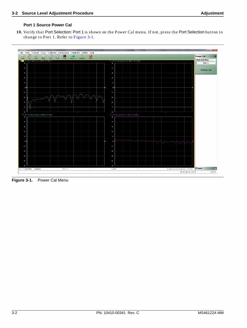
Port 1 Source Power Cal
10. Verify that Port Selection: Port 1 is shown on the Power Cal menu. If not, press the Port Selection button to change to Port 1. Refer to Figure 3-1.
Figure 3-1. Power Cal Menu
Adjustment 3-2 Source Level Adjustment Procedure
MS46122A MM PN: 10410-00341 Rev. C 3-3
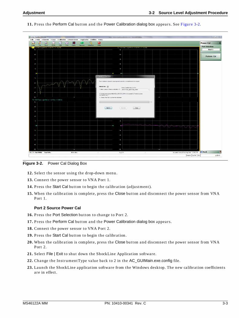
11. Press the Perform Cal button and the Power Calibration dialog box appears. See Figure 3-2.
12. Select the sensor using the drop-down menu.
13. Connect the power sensor to VNA Port 1.
14. Press the Start Cal button to begin the calibration (adjustment).
15. When the calibration is complete, press the Close button and disconnect the power sensor from VNA Port 1.
Port 2 Source Power Cal
16. Press the Port Selection button to change to Port 2.
17. Press the Perform Cal button and the Power Calibration dialog box appears.
18. Connect the power sensor to VNA Port 2.
19. Press the Start Cal button to begin the calibration.
20. When the calibration is complete, press the Close button and disconnect the power sensor from VNA Port 2.
21. Select File | Exit to shut down the ShockLine Application software.
22. Change the InstrumentType value back to 2 in the AC_GUIMain.exe.config file.
23. Launch the ShockLine application software from the Windows desktop. The new calibration coefficients are in effect.
Figure 3-2. Power Cal Dialog Box

3-3 IF Adjustment Procedure Adjustment
3-4 PN: 10410-00341 Rev. C MS46122A MM
3-3 IF Adjustment ProcedureThis section provides the procedure to restore or optimize the operation of the MS46122A/B related to the IF level in the VNA receivers.
Equipment Required
• For Instruments with N(f) Test Ports:
• Anritsu Model 3670K50-2 Through Cable
• Anritsu Model 34NK50 N(m) to K(m) Adapter
• Anritsu Model 34NKF50 N(m) to K(f) Adapter
• For Instruments with K(m) Test Ports:
• Anritsu Model 3670K50-2 Through Cable
• Anritsu Model 33KFKF50B K(f) to K(f) Adapter
Procedure
1. Power on the VNA and allow the instrument to warm up for at least 45 minutes.
2. On the PC controller, launch the ShockLine application software.
3. Connect the through cable between Port 1 and Port 2.
4. Press the Calibration button on the right side menu.
5. Press the IF Cal button and follow the prompt to perform the calibration.
6. Select File | Exit to shut down the ShockLine Application software.
7. Launch the ShockLine Application software from the Windows desktop. The new calibration coefficients are in effect.
NotePerforming the IF adjustment procedure is normally not required after the VNA module assembly has been replaced. Each replacement VNA module is fully pre-calibrated / pre-adjusted prior to shipping from the factory.

Adjustment 3-4 Time Base Adjustment Procedure
MS46122A MM PN: 10410-00341 Rev. C 3-5
3-4 Time Base Adjustment ProcedureThis section provides the procedure to adjust the internal Time Base in the MS46122A/B.
Equipment Required
• Instruments with N(f) Test Ports:
• Anritsu Model MF2412x Frequency Counter with Option 3
• Anritsu Model 3670K50-2 Through Cable
• Anritsu Model 34NK50 N(m) to K(m) Adapter
• Anritsu Model 34NKF50 N(m) to K(f) Adapter
• Instruments with K(m) Test Ports:
• Anritsu Model MF2412x Frequency Counter with Option 3
• Anritsu Model 3670K50-2 Through Cable
• Anritsu Model 34NKF50 N(m) to K(f) Adapter
Procedure
1. Power on the Frequency Counter and then press the Preset key.
2. Power on the VNA and allow the instrument to warm up for at least 45 minutes.
3. On the PC controller, launch the ShockLine application software.
4. Connect the through cable between the Frequency Counter Input 1 and VNA Port 1.
5. On the PC controller right-side menu, click the System button, then the Diagnostics button.
6. The Diagnostics Access dialog box appears providing an entry field to enter the diagnostics access password as shown in Figure 3-3.
7. Enter “ModVna” in the password field and click OK.
8. Click the Hardware Cal button, then the Time Base Cal button.
9. Change the DAC Number value in the Time Base Calibration dialog box as shown in Figure 3-4 so that the frequency displayed on the frequency counter is within 5 GHz ± 2 kHz.
NotePerforming the Time Base adjustment procedure is normally not required after the VNA module assembly has been replaced. Each replacement VNA module is fully pre-calibrated / pre-adjusted prior to shipping from the factory.
Figure 3-3. Diagnostics Access Dialog Box

3-4 Time Base Adjustment Procedure Adjustment
3-6 PN: 10410-00341 Rev. C MS46122A MM
10. Click the Close button when done.
Figure 3-4. Time Base Calibration Dialog Box
MS46122A MM PN: 10410-00341 Rev. C 4-1
Chapter 4 — Troubleshooting
4-1 IntroductionThis chapter provides information about troubleshooting tests that can be used to check the MS46122A/B Vector Network Analyzer for proper operation. These tests are intended to be used as a troubleshooting tool for identifying the faulty components and checking the functionality of internal components and sub-assemblies in the MS46122A/B VNA.
Only qualified service personnel should replace internal assemblies. Major subassemblies that are shown in the replaceable parts list are typically the items that may be replaced. Because they are highly fragile, items that must be soldered may not be replaced without special training. Removal of RF shields from PC boards or adjustment of screws on or near the RF shields will de-tune sensitive RF circuits and result in degraded instrument performance.
4-2 General Safety WarningsMany of the troubleshooting procedures presented in this chapter require the removal of the instrument covers to access sub-assemblies and modules. When using these procedures, please observe the warning and caution notices.
CautionMany assemblies and modules in the MS46122A/B VNA contain static-sensitive components. Improper handling of these assemblies and modules may result in damage to the assemblies and modules. Always observe the static-sensitive component handling precautions.

4-3 Troubleshooting Test – Non-Ratio Power Level Check Troubleshooting
4-2 PN: 10410-00341 Rev. C MS46122A MM
4-3 Troubleshooting Test – Non-Ratio Power Level CheckThe non-ratio power level check verifies the VNA module assembly for faults.
Equipment Required
• For Instruments with N(f) Test Ports:
• Anritsu Model 3670K50-2 RF Coaxial Cable
• Anritsu Model 34NK50 N(m) to K(m) Adapter
• Anritsu Model 34NKF50 N(m) to K(m) Adapter
• For Instruments with K(m) Test Ports:
• Anritsu Model 3670K50-2 RF Coaxial Cable
• Anritsu Model 33KFKF50B K(f) to K(f) Adapter
Procedure
1. Power on the PC controller.
2. For instruments with N(f) test ports, install the 34NK50 and 34NKF50 adapters to the 3670K50-2 RF coaxial cable to convert both ends into N(m) connector port.
3. For instruments with K(m) test ports, install the 33KFKF50B to the male end of the 3670K50-2 RF coaxial cable.
4. Turn on the MS46122A/B.
5. Connect the coaxial cable between test port 1 and test port 2.
6. Select Trace 1 and then select Display | Trace Format. Set Trace Format to Log Mag.
7. Select Response | User-defined. The User-defined menu appears.
8. Set Numerator to A1, Denominator to 1, and Driver Port to Port 1.
9. Use a mouse to move the reference line to one graticule below top scale.
10. Repeat step 4 through step 7 for Trace 2, setting Numerator to B2, Denominator to 1, and Driver Port to Port 1.
11. Repeat Steps 4 through step 7 for Trace 3, setting Numerator to B1, Denominator to 1, and Driver Port to Port 2.
12. Repeat Step 4 through step 7 for Trace 4, setting Numerator to A2, Denominator to 1, and Driver Port to Port 2.
13. Observe whether any portions of these traces show any abnormality (for example, very low power level).
Troubleshooting 4-4 Troubleshooting Turn-on Problems
MS46122A MM PN: 10410-00341 Rev. C 4-3
4-4 Troubleshooting Turn-on Problems
Unit Cannot Power Up
Unit cannot power up; Power LED is not lit when the Power key is toggled:
1. Use a digital volt meter to verify that +12 V is present at the output jack of the AC/DC adapter.
a. If +12 V is not present, replace the AC/DC adapter.
b. If +12 V is present, then replace the VNA assembly.
ShockLine Application Cannot Launch
Unit can power up, but the ShockLine application does not launch on the PC controller:
1. The ShockLine application software update may not have completed. Re-install the software.
2. If the problem still exists, verify that the PC controller USB port is functioning properly or verify that the MS46122A/B is working properly with another PC controller.
3. If the MS46122A/B is not working with another PC controller, replace the VNA assembly.
4-5 Troubleshooting Operating Problems
Frequency Related Problems
If the instrument exhibits frequency related problem, do the following:
1. Perform a time base calibration (refer to Section 3-4 “Time Base Adjustment Procedure”).
2. Apply an external 10 MHz reference to the front panel 10 MHz Ref In.
3. If the problem does not show with the external reference, the problem is in the internal reference oscillator. Replace the VNA assembly.
RF Power Related Problems
If the instrument exhibits RF power related problems, do the following:
1. Perform the “Troubleshooting Test – Non-Ratio Power Level Check” on page 4-2.
2. If the power level shows any abnormality, do the following:
a. Verify that the connection between the test port adapter and the VNA assembly is secure. Re-torque if necessary.
b. Verify that the test port adapter is not worn or damaged. Replace the test port adapter if necessary.
c. Replace the VNA assembly.

4-6 Troubleshooting Measurement Problems Troubleshooting
4-4 PN: 10410-00341 Rev. C MS46122A MM
4-6 Troubleshooting Measurement ProblemsIf the MS46122A/B measurement quality is suspect, the following paragraphs provide guidelines and hints for determining possible quality problems.
VNA Measurement Quality
The quality of MS46122A/B VNA measurements is determined by the following:
• The condition of the MS46122A/B.
• The quality and condition of the interface connections and connectors.
• The quality and condition of the calibration components, through cables, adapters, and fixtures.
• The surrounding environmental conditions at the time of the measurement.
• The selection and performance of the calibration for the DUT being measured.
Checking Possible Measurement Problems
When determining possible measurement problems, check the following items:
1. Check the DUT and the calibration conditions:
a. Ensure that the calibration components coefficients data has been installed into the VNA for the calibration kit in use.
b. Ensure that the proper calibration was done for the device being measured:
• For high insertion-loss device measurements, the calibration should include isolation, high number of averages, and a narrow IF bandwidth setting during calibration.
• For high return-loss device measurements, a high quality precision load should be used during calibration.
c. Check the condition of mating connectors and their pin depth.
d. If possible, measure an alternate known good device.
e. Check if the environment is stable enough for the accuracy required for the device measurement.
• The VNA should not be subjected to variations in temperature.
• The VNA should not be placed in direct sunlight or next to a changing cooling source, such as a fan or air conditioning unit.
2. Check the calibration using known good components from the calibration kit. If measurements of these devices do not produce good results, try the following:
a. Check through-cable stability including connector condition and pin depth. Replace with a known good cable, if necessary.
b. Check the condition and pin depth of the calibration kit components. Replace with known good components, if necessary.
c. Check the condition and pin depth of the test port adapters. Replace with known good adapters, if necessary.
3. Check the system performance as described in Chapter 2, “Performance Verification”
MS46122A MM PN: 10410-00341 Rev. C 5-1
Chapter 5 — Assembly Removal and Replacement
5-1 IntroductionThis chapter describes the removal and replacement procedures for the various internal assemblies. Illustrations (drawings or photographs) in this manual may differ slightly from the instrument that you are servicing, but the basic removal and replacement functions will remain as specified. The illustrations are meant to provide assistance with identifying parts and their locations.
5-2 Electrostatic Discharge Prevention An ESD safe work area and proper ESD handling procedures that conform to ANSI/ESD S20.20-1999 or ANSI/ESD S20.20-2007 is mandatory to avoid ESD damage when handling subassemblies or components found in the MS46122A/B Vector Network Analyzer.
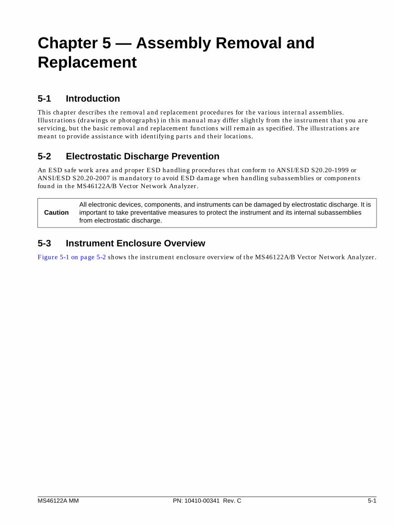
5-3 Instrument Enclosure OverviewFigure 5-1 on page 5-2 shows the instrument enclosure overview of the MS46122A/B Vector Network Analyzer.
CautionAll electronic devices, components, and instruments can be damaged by electrostatic discharge. It is important to take preventative measures to protect the instrument and its internal subassemblies from electrostatic discharge.
5-3 Instrument Enclosure Overview Assembly Removal and Replacement
5-2 PN: 10410-00341 Rev. C MS46122A MM
1 Front Bumper
2 Rear Bumper
3 Bottom Foot
4 Bottom Foot Mounting Screws
Figure 5-1. MS46122A/B Instrument Enclosure Overview
1
2
34X
44X

Assembly Removal and Replacement 5-4 Disassembly Procedure
MS46122A MM PN: 10410-00341 Rev. C 5-3
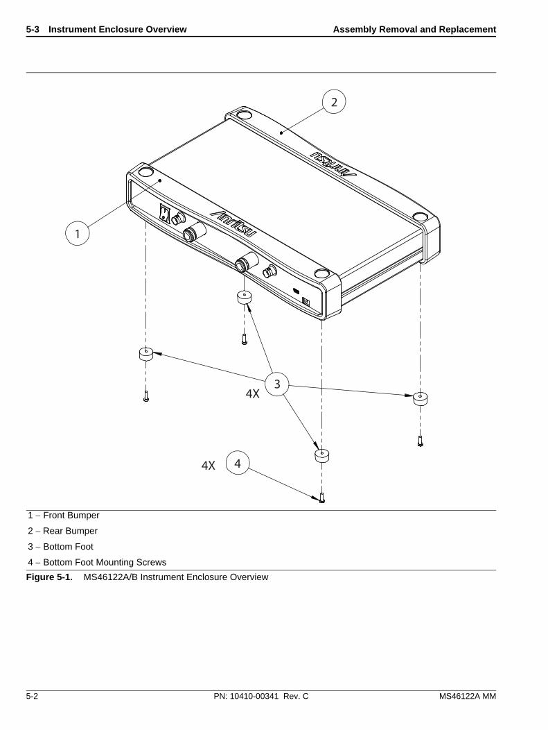
5-4 Disassembly ProcedureUse this procedure to prepare the MS46122A/B for removal and replacement procedures for all of its replaceable components. All replacement components require this common disassembly procedure.
Common Disassembly Procedure
1. Prepare a clean and static free work area. Make sure that the work area is well grounded. Cover the work surface with a soft, clean anti-static mat.
2. Provide all personnel with appropriate anti-static grounding wrist straps and similar equipment.
3. Power down the VNA and then unplug the AC power cord and USB cable.
4. Place the VNA on the anti-static mat.
5. Refer to Figure 5-2 on page 5-4 and remove the top case as follows:
a. Remove the front and rear bumpers.
b. Remove the six screws that secure the top bumper mounting strips to the top case.
c. Remove the four side mounting screws.
d. Remove the three rear panel screws.
e. Remove the top case.
6. Refer to Figure 5-2 on page 5-4 and remove the front panel assembly as follows:
a. Place the instrument upside down on the working surface.
b. Remove the two screws that secure the front bottom bumper mounting strip to the bottom case.
c. Remove the four screws that secure the front panel assembly to the bottom case.
d. Place the instrument with its top side facing upward.
e. Unplug the 10 MHz Reference In cable from J30 of the VNA assembly.
f. Unplug the Trigger In cable from J34 of the VNA assembly.
g. Unplug the front panel ribbon cable from the VNA assembly.
h. For units with N(f) test ports, disconnect the Port 1 coaxial cable from J1 of the VNA assembly and then disconnect the Port 2 coaxial cable from J2 of the VNA assembly.
i. For units with K(m) test ports, disconnect both the SMA(m) end of the Port 1 test port adapter and the Port 2 test port adapter from the VNA assembly.
j. Carefully remove the front panel assembly from the bottom case.
5-4 Disassembly Procedure Assembly Removal and Replacement
5-4 PN: 10410-00341 Rev. C MS46122A MM
1. Top Case2. Bumper Mounting Strips3. Top Bumper Mounting Strip Screws4. Rear Screws5. Side Mounting Screws6. Bottom Bumper Mounting Strip Screws
Figure 5-2. MS46122A/B Dis-assembling Drawing
1
2
3
4
5
5
6
2X
2X
2
3X
4X
6X
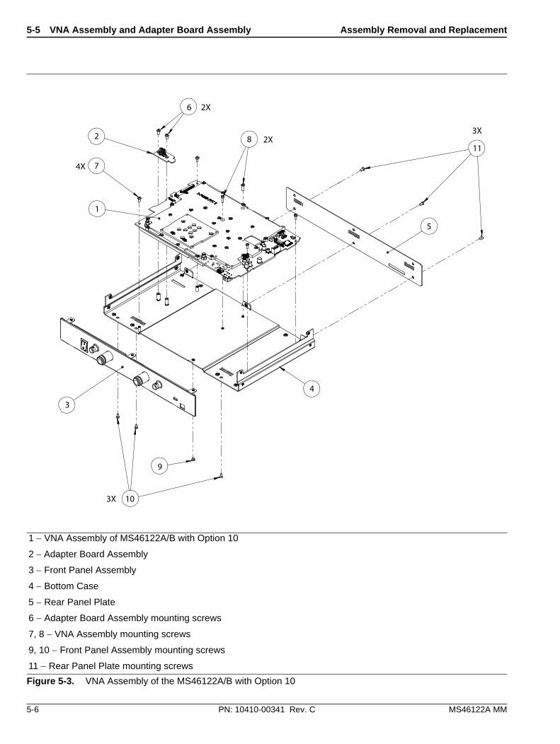
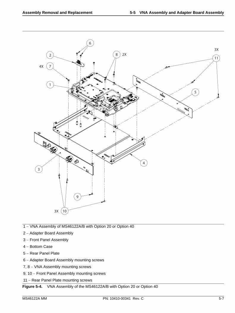
Assembly Removal and Replacement 5-5 VNA Assembly and Adapter Board Assembly
MS46122A MM PN: 10410-00341 Rev. C 5-5
5-5 VNA Assembly and Adapter Board AssemblyUse this procedure to replace the VNA Assembly and Adapter Board Assembly. The VNA Assembly is secured to the bottom case using six (6) Phillips screws. The Adapter Board Assembly which is replaced separately is plugged into J31 of the VNA Assembly.
Replacement Parts
• VNA Assembly of the MS46122A with Option 10 – ND81301<R>
• VNA Assembly of the MS46122A with Option 20 – ND81302<R>
• VNA Assembly of the MS46122A with Option 40 – ND81303<R>
• VNA Assembly of the MS46122B with Option 10 – 3-ND83417<R>
• VNA Assembly of the MS46122B with Option 20 – 3-ND83418<R>
• VNA Assembly of the MS46122B with Option 40 – 3-ND83419<R>
• Adapter Board Assembly – 3-80719-3
Reference Figures
• Figure 5-3 on page 5-6 shows the VNA assembly of the MS46122A/B with Option 10.
• Figure 5-4 on page 5-7 shows the VNA assembly of the MS46122A/B with Option 20 or Option 40.
5-5 VNA Assembly and Adapter Board Assembly Assembly Removal and Replacement
5-6 PN: 10410-00341 Rev. C MS46122A MM
1 VNA Assembly of MS46122A/B with Option 10
2 Adapter Board Assembly
3 Front Panel Assembly
4 Bottom Case
5 Rear Panel Plate
6 Adapter Board Assembly mounting screws
7, 8 VNA Assembly mounting screws
9, 10 Front Panel Assembly mounting screws
11 Rear Panel Plate mounting screws
Figure 5-3. VNA Assembly of the MS46122A/B with Option 10
1
2
3
4
5
6
74X
8
2X
2X
9
103X
11
3X
Assembly Removal and Replacement 5-5 VNA Assembly and Adapter Board Assembly
MS46122A MM PN: 10410-00341 Rev. C 5-7
1 VNA Assembly of MS46122A/B with Option 20 or Option 40
2 Adapter Board Assembly
3 Front Panel Assembly
4 Bottom Case
5 Rear Panel Plate
6 Adapter Board Assembly mounting screws
7, 8 VNA Assembly mounting screws
9, 10 Front Panel Assembly mounting screws
11 Rear Panel Plate mounting screws
Figure 5-4. VNA Assembly of the MS46122A/B with Option 20 or Option 40
1
2
3
4
5
6
74X
8 2X
9
103X
11
3X
5-5 VNA Assembly and Adapter Board Assembly Assembly Removal and Replacement
5-8 PN: 10410-00341 Rev. C MS46122A MM
Replacement Procedure
1. Remove the top case and front panel assembly as described in the “Common Disassembly Procedure” on page 5-3.
2. Remove the two Phillips screws that secure the Adapter Board assembly.
3. Unplug the Adapter Board assembly from the VNA assembly.
4. Remove the six Phillips screws that secure the VNA assembly as shown in Figure 5-3 on page 5-6 for units with Option 10 or in Figure 5-4 on page 5-7 for units with Option 20 or Option 40.
5. Remove the VNA assembly.
6. Install the replacement VNA assembly into the bottom case.
7. Secure the VNA assembly with screws that were removed in Step 4.
8. Install the Adapter Board assembly to J31 of the VNA assembly and secure with the screws that were removed in Step 3.
9. For an MS46122A/B with Option 10:
a. Re-connect the Port 1 coaxial cable to J1 connector of the VNA assembly.
b. Re-connect the Port 2 coaxial cable to J2 connector of the VNA assembly.
c. Torque the cable connection to 8 in-lb.
d. Install the front panel assembly.
10. For an MS46122A/B with Option 20 or Option 40:
a. Re-connect Port 1 test port adapter and Port 2 test port adapter to the receiver module of the VNA assembly.
b. Torque the connection to 8 in-lb.
c. Secure the front panel assembly with screws.
11. Re-connect the 10 MHz Reference In cable to J30 of the VNA assembly.
12. Re-connect the Trigger In cable to J34 of the VNA assembly.
13. Install the top case.
14. Install the bumper mounting strips.
15. Install the bumpers.

Assembly Removal and Replacement 5-6 Front Panel LED PCB Assembly
MS46122A MM PN: 10410-00341 Rev. C 5-9
5-6 Front Panel LED PCB AssemblyUse this procedure to replace the front panel LED PCB assembly.
The front panel LED PCB assembly is secured to the front panel plate with five (5) kep nuts.
Replacement Part
• Front Panel LED PCB Assembly for MS46122A – ND81018
• Front Panel LED PCB Assembly for MS46122B – 3-ND81018
Reference Figure
• Figure 5-5 below shows the location of the front panel LED PCB assembly.
1 Front Panel LED PCB Assembly
2 Nylon washers
3 Kep Nuts
Figure 5-5. Front Panel LED PCB Assembly
1
2
3
5-6 Front Panel LED PCB Assembly Assembly Removal and Replacement
5-10 PN: 10410-00341 Rev. C MS46122A MM
Replacement Procedure
1. Remove the top case and front panel assembly as described in the “Common Disassembly Procedure” on page 5-3.
2. Unplug the ribbon cable from J1 of the front panel LED PCB assembly.
3. Remove the five (5) kep nuts that secure the front panel LED PCB assembly to the front panel plate.
4. Remove the front panel LED PCB assembly.
5. Install the replacement front panel LED PCB assembly to the front panel and secure it with the kep nuts that were removed in Step 3.
6. Install the front panel assembly to the bottom case.
7. Re-connect the ribbon cable to J1 of the front panel LED PCB assembly.
8. Install the top case.
9. Install the bumper mounting strips
10. Install the bumpers.
NoteBe careful not to lose the nylon washers that are placed between the front panel plate and the front panel LED PCB assembly.

Assembly Removal and Replacement 5-7 Test Port Adapter
MS46122A MM PN: 10410-00341 Rev. C 5-11
5-7 Test Port AdapterUse this procedure to replace the front panel test port adapters.
Replacement Part
• Test Port Adapter of MS46122A with Option 10 – 3-513-122
• Test Port Adapter of MS46122B with Option 10 – 3-82848
• Test Port Adapter of MS46122A/B with Option 20 or Option 40 – 3-75651
Reference Figures
• Figure 5-6 below shows how the N(f) test port adapters are mounted to the front panel of MS46122A.
• Figure 5-8 on page 5-13 shows how the K(m) test port adapters are mounted to the front panel. .
1 Front Panel Plate
2 Power Switch
3 10 MHz Reference In cable
4 Trigger In Cable
5 Test Port Adapters (Washer and Hex Nut are included in replacement package)
6 Front Panel Assembly
7 Test Port Coaxial Cables
Figure 5-6. Test Port Adapters of the MS46122A with Option 10
1
2
4
5
6
7
3

5-7 Test Port Adapter Assembly Removal and Replacement
5-12 PN: 10410-00341 Rev. C MS46122A MM
1 Front Panel Plate
2 Power Switch
3 10 MHz Reference In cable
4 Trigger In Cable
5 Test Port Adapters
6 Front Panel Assembly
7 Test Port Coaxial Cables
8 – Hex Nuts
Figure 5-7. Test Port Adapters of the MS46122B with Option 10
1
23
8
4
5
6
7

Assembly Removal and Replacement 5-7 Test Port Adapter
MS46122A MM PN: 10410-00341 Rev. C 5-13
1 Front Panel Plate
2 Power Switch
3 10 MHz Reference In cable
4 Trigger In Cable
5 Test Port Adapters (Washer and Hex Nut are included in replacement package but not shown in this figure)
6 Front Panel Assembly
Figure 5-8. Test Port Adapters of the MS46122A/B with Option 20 or Option 40
1
2
4
5
6
3
5-7 Test Port Adapter Assembly Removal and Replacement
5-14 PN: 10410-00341 Rev. C MS46122A MM
Replacement Procedure
1. Remove the top case and front panel assembly as described in the “Common Disassembly Procedure” on page 5-3.
2. Disconnect the flexible coaxial cable from the SMA(f) connector of the test port adapter.
3. For MS46122A with Option 10 and MS46122A/B with Option 20 or 40, use a ratchet wrench with a 1/4 inch deep socket to remove the hex nut that secures the test port adapter to the front panel.
4. For MS46122B with Option 10, remove the two (2) hex nuts that secure the test port adapter to the front panel.
5. Remove the test port adapter from the front panel.
6. Install the replacement test port adapter to the front panel. Install the washer and then the hex nut. Tighten the hex nut with fingers.
7. For MS46122A with Option 10 and MS46122A/B with Option 20 or 40, use a ratchet wrench with the 1/4 inch deep socket to tighten the hex nut. Torque to 15 ft-lb (~20.33 N-m).
8. For MS46122B with Option 10, use a wrench to tighten the hex nuts.
9. Re-connect the flexible coaxial cable to the SMA(f) connector of the test port adapter.
10. Install the top cover.
MS46122A MM PN: 10410-00341 Rev. C A-1
Appendix A — Test Records
A-1 IntroductionThis appendix provides a test record that can be used to record the performance of the ShockLine MS46122A.
Make a copy of the following test record pages and document the measured values each time performance verification is performed. Continuing to document this process for each performance verification session provides a detailed history of the instrument‘s performance.
The following test record form is available:
• “ShockLine MS46122A/B Test Record” on page A-2

A-2 ShockLine MS46122A/B Test Record Test Records
A-2 PN: 10410-00341 Rev. C MS46122A MM
Instrument Information
A-2 ShockLine MS46122A/B Test Record
System Performance Verification
This test is automated using the System Verification software that is included with 3663-x or 3668-x Verification Kits.
Test Data Report generated by System Verification software is attached. [ ]
Serial Number: Firmware Revision: Operator:
Options: Date:
NotePass/Fail criteria is determined from EnR, EnR <=1 = PASS, EnR >1 = FAIL
Where EnR = [Ma-Mb/sqrt(Ua^2+Ub^2)]

Numerics to W
MS46122A MM PN: 10410-00341 Rev. C Index-1
IndexNumerics
20 dB Attenuation Standard . . . . . . . . . . . . . . . . 2-525 Ohm Mismatch (Beatty) Standard . . . . . . . . . 2-550 dB Attenuation Standard . . . . . . . . . . . . . . . . 2-550 Ohm Air Line Standard . . . . . . . . . . . . . . . . . 2-5
AAnritsu Service Center . . . . . . . . . . . . . . . . . . . . . 1-2Available Options . . . . . . . . . . . . . . . . . . . . . . . . . 1-1
BBeatty Standards
25 Ohm Mismatch (Beatty) Standard . . . . . . 2-5
CCables
Preshapping . . . . . . . . . . . . . . . . . . . . . . . . . . 2-6Calibration . . . . . . . . . . . . . . . . . . . . . . . . . . . . . . 1-2cautions
electrostatic discharge (ESD) . . . . . . . . . . . . 5-1non-Anritsu test equipment . . . . . . . . . . . . . 2-4use torque wrench . . . . . . . . . . . . . . . . . . 2-7, 2-9
Certification . . . . . . . . . . . . . . . . . . . . . . . . . . . . . 1-2
Eelectrostatic discharge (ESD) . . . . . . . . . . . . . . . . 5-1
IIdentification Number . . . . . . . . . . . . . . . . . . . . . 1-1Impedance Transfer Standards . . . . . . . . . . . . . . 2-5
MMaintain Operating System Integrity . . . . . . . . . 1-2Minimize Vibration . . . . . . . . . . . . . . . . . . . . . . . . 2-6
PPerformance Verification
Special Precautions . . . . . . . . . . . . . . . . . . . . 2-6Standard Conditions . . . . . . . . . . . . . . . . . . . 2-3
Preshape Test Port Cables . . . . . . . . . . . . . . . . . . .2-6Preshapping . . . . . . . . . . . . . . . . . . . . . . . . . . . . . .2-6Process for Creation and Use of a Verification Kit 2-2
RRecommended Test Equipment . . . . . . . . . . . . . . .1-3Relative Humidity . . . . . . . . . . . . . . . . . . . . . . . . .2-3Repair Service . . . . . . . . . . . . . . . . . . . . . . . . . . . .1-2
SStandard Accessories . . . . . . . . . . . . . . . . . . . . . . .1-1Standards
20 dB Attenuation . . . . . . . . . . . . . . . . . . . . . .2-525 Ohm Mismatch (Beatty) . . . . . . . . . . . . . . .2-550 dB Attenuation . . . . . . . . . . . . . . . . . . . . . .2-550 Ohm Air Line . . . . . . . . . . . . . . . . . . . . . . .2-5Impedance Transfer Standards . . . . . . . . . . .2-5
TTemperature . . . . . . . . . . . . . . . . . . . . . . . . . . . . . .2-3Test Port Cables . . . . . . . . . . . . . . . . . . . . . . . . . . .2-6Traceability . . . . . . . . . . . . . . . . . . . . . . . . . . . . . . .2-1
UUncertainty . . . . . . . . . . . . . . . . . . . . . . . . . . . . . . .2-1
VVerification
Result Determination . . . . . . . . . . . . . . . . . . .2-5Results Quality . . . . . . . . . . . . . . . . . . . . . . . .2-6System Verification Procedure . . . . . . . . . . . .2-6
WWarm-Up Time . . . . . . . . . . . . . . . . . . . . . . . . . . . .2-3Windows OS Updates . . . . . . . . . . . . . . . . . . . . . . .1-2

Index-2 PN: 10410-00341 Rev. C MS46122A MM


Anritsu utilizes recycled paper and environmentally conscious inks and toner.
Anritsu Company490 Jarvis Drive
Morgan Hill, CA 95037-2809USA
http://www.anritsu.com


![Champion. (Arcadia, Florida) 1908-10-08 [p ].ufdcimages.uflib.ufl.edu/UF/00/07/58/90/00088/00341.pdfCHAMPIONTHor-1 irVDI3ARTMENTt-r Tjr voluwecol1ectionoHVordswort-hstetersmany FATHERS](https://static.fdocuments.in/doc/165x107/5b3ae8377f8b9a26728beed7/champion-arcadia-florida-1908-10-08-p-irvdi3artmentt-r-tjr-voluwecol1ectionohvordswort-hstetersmany.jpg)