SHENZHEN YAOXINGYANG CO.,LTD. J204A PDF...
19
SHENZHEN YAOXINGYANG CO.,LTD. J204A PDF 1 SPECIFICATION FOR APPROVAL Product Type: Character Type STN Dot Matrix LCD Module Part No.: J2004A-GFDN-DYNC Customer: Customer Part No.: Date: APPOVED SIGNATURES BLUE MOON Customer BLUE MOON DISPLAY CO.,LTD
Transcript of SHENZHEN YAOXINGYANG CO.,LTD. J204A PDF...

SHENZHEN YAOXINGYANG CO.,LTD. J204A PDF
1
SPECIFICATION FOR APPROVAL
Product Type: Character Type STN Dot Matrix LCD Module
Part No.: J2004A-GFDN-DYNC
Customer:
Customer Part No.: Date:
APPOVED SIGNATURES
BLUE MOON Customer
BLUE MOON DISPLAY CO.,LTD

SHENZHEN YAOXINGYANG CO.,LTD. J204A PDF
2
1 . REVISION RECORD
2. GENERAL SPECIFICATION
3. OUTLINE DEMENSION:
4. BLOCK DIAGRAM
5.ABSOLUTE MAXIMUM RATINGS
6.ELECTRICAL CHARACTERISTICS
7.ABSOLUTE MAXIMUM RATINGS FOR LED BACKLIGHT
8.PIN ASSIGNMENT
9.MPU INTERFACE
10.REFLECTOR OF SCREEN AND DIPLAY RAM
11.DISPLAY CONTROL INSTRUCTION
12.OPTICAL CHARACTERISTICS
13.POWER SUPPLY SCHEMATICS
14.APPLICATION EXAMPLE
15. PRECAUTION FOR USING LCM
SHENZHEN YAOXINGYANG CO.,LTD. J204A PDF
3
1 . REVISION RECORD
REV DATA PAGES DESCRIPTION
SHENZHEN YAOXINGYANG CO.,LTD. J204A PDF
4
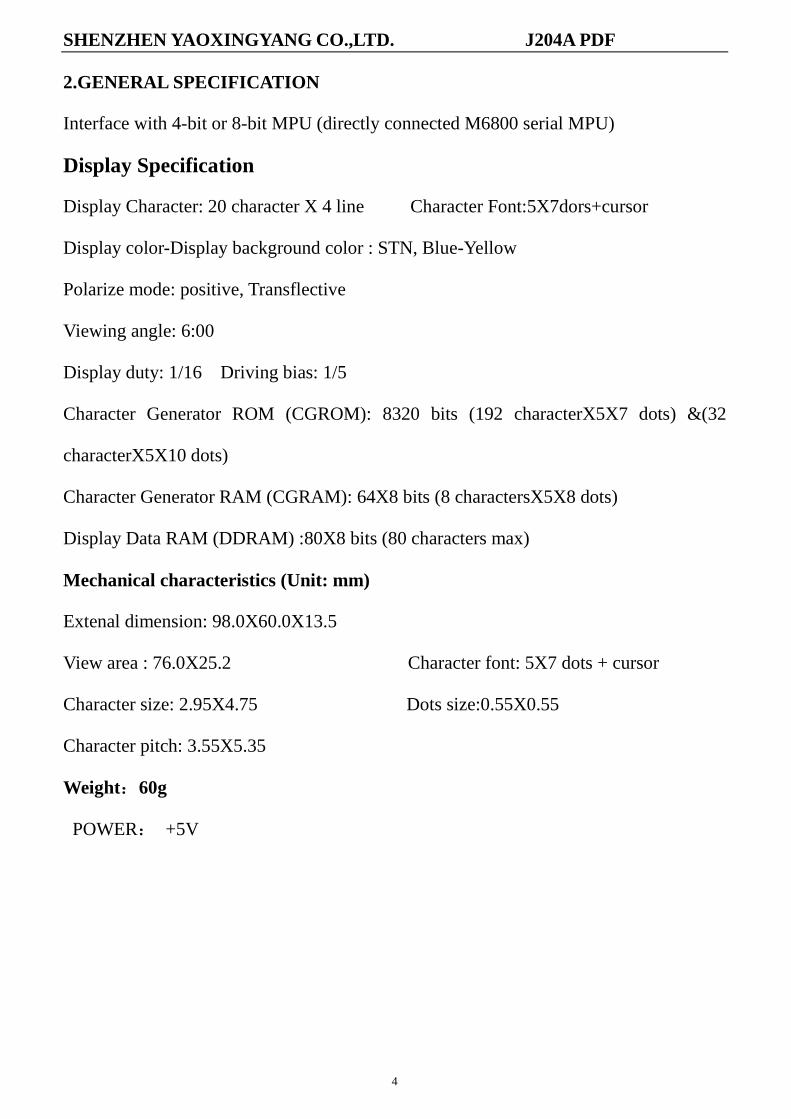
2.GENERAL SPECIFICATION
Interface with 4-bit or 8-bit MPU (directly connected M6800 serial MPU)
Display Specification
Display Character: 20 character X 4 line Character Font:5X7dors+cursor
Display color-Display background color : STN, Blue-Yellow
Polarize mode: positive, Transflective
Viewing angle: 6:00
Display duty: 1/16 Driving bias: 1/5
Character Generator ROM (CGROM): 8320 bits (192 characterX5X7 dots) &(32
characterX5X10 dots)
Character Generator RAM (CGRAM): 64X8 bits (8 charactersX5X8 dots)
Display Data RAM (DDRAM) :80X8 bits (80 characters max)
Mechanical characteristics (Unit: mm)
Extenal dimension: 98.0X60.0X13.5
View area : 76.0X25.2 Character font: 5X7 dots + cursor
Character size: 2.95X4.75 Dots size:0.55X0.55
Character pitch: 3.55X5.35
Weight:60g
POWER: +5V

SHENZHEN YAOXINGYANG CO.,LTD. J204A PDF
5
3. OUTLINE DEMENSION:
4. BLOCK DIAGRAM:

SHENZHEN YAOXINGYANG CO.,LTD. J204A PDF
6
5.Absolute Maximum Ratings
Standard Value Item Symbol Condition Min Max
Unit
Supply Voltage for logic Vdd -0.3 7.0 V Supply Voltage for LCD Vlcd Vdd-10.0 Vdd+0.3 V Input Voltage Vi -0.3 Vdd+0.3 V Operating Temperature(T) Top - 0 50 ℃ Storage Temperature(T) Tstg - -10 60 ℃
6.ELECTRICAL SPECIFICATIONS(Ta=250C,Vdd=5.0V)
Standard Value Item Symbol Condition Min Type Max
Unit
Supply Voltage for logic Vdd-GND - 4.5 5.0 5.5 V Supply Current for logic Idd - 1.0 - mA Driving Current for LCD Iee - 0.6 - mA Driving Voltage for LCD Vlcd 4.4 4.7 5.0 V Input Voltage H level Vih 2.2 - Vdd V Input Voltage L level Vil
Vdd=5V
-0.3 - 0.6 V Output Voltage H Voh Ioh=-0.205mA 2.4 - - V Output Voltage L Vol Io1=1.2mA - - 0.4 V
7.Absolute Maximum Ratings For Bottom LED Backlight
Parameter Symbol Test condition Min Type Max Unit LED Forward Consumption Current If - 120 180 mA
LED Allowable Dissipation Pd Ta=250C Vf=4.2V - 384 630 mW
8. Pin assignment
Pin NO. Symbol Function Remark 1 Vss 0V 2 Vdd +5V 3 Vo
Power Supply
For LCD Variable 4 RS Register Select (H: Data L: Instruction) 5 R/W L: MPU to LCM H: LCM to MPU 6 E Enable 7 DB0 Data Bit 0 8 DB1 Data Bit 1 9 DB2 Data Bit 2 10 DB3 Data Bit 3 11 DB4 Data Bit 4 12 DB5 Data Bit 5 13 DB6 Data Bit 6 14 DB7 Data Bit 7 15 A Anode of LED Unit 16 K Cathode of LED Unit

SHENZHEN YAOXINGYANG CO.,LTD. J204A PDF
7
9. MPU Interface (Vdd=4.5V~5.5V, Ta=-30~+85℃)
Mode Characteristic Symbol Min. Type Max Unit E Cycle Time tC 500 - - E Rise/Fall Time tR,tF - - 20 E Pulse Width (High, Low) tPW 230 - - R/W and RS Setup time tSP1 40 - - R/W and RS Hold Time tHD1 10 - - Data Setup Time tSP2 80 - -
Write Mode
Data Hold Time tHD2 10 - -
ns
E Cycle Time tC 500 - - E Rise/Fall Time tR,tF - - 20 E Pulse Width(High, Low) tPW 230 - - R/W and RS Setup Time tSP1 40 - - R/W and RS Hold Time tHD2 10 - - Data Output Delay Time tD - - 120
Read Mode
Data Hold Time tHD2 5 - -
ns
IC Specifications
See The Reference of Sunplus Data Book-----SPLC780D
Timing diagram
(WRITE)
E
R/W
Valid Data
Valid Data
DB0-DB7
(READ)DB0-DB7
VIH1
VIL1
VIH1
VIL1
VIH1
VIL1 VIL1
VIH1
VIL1
VIH1 VIH1
VIL1
VIH1
VIL1
VIH1
VIL1
VIH1
VIL1
VIH1
VIL1
RS
SHENZHEN YAOXINGYANG CO.,LTD. J204A PDF
8
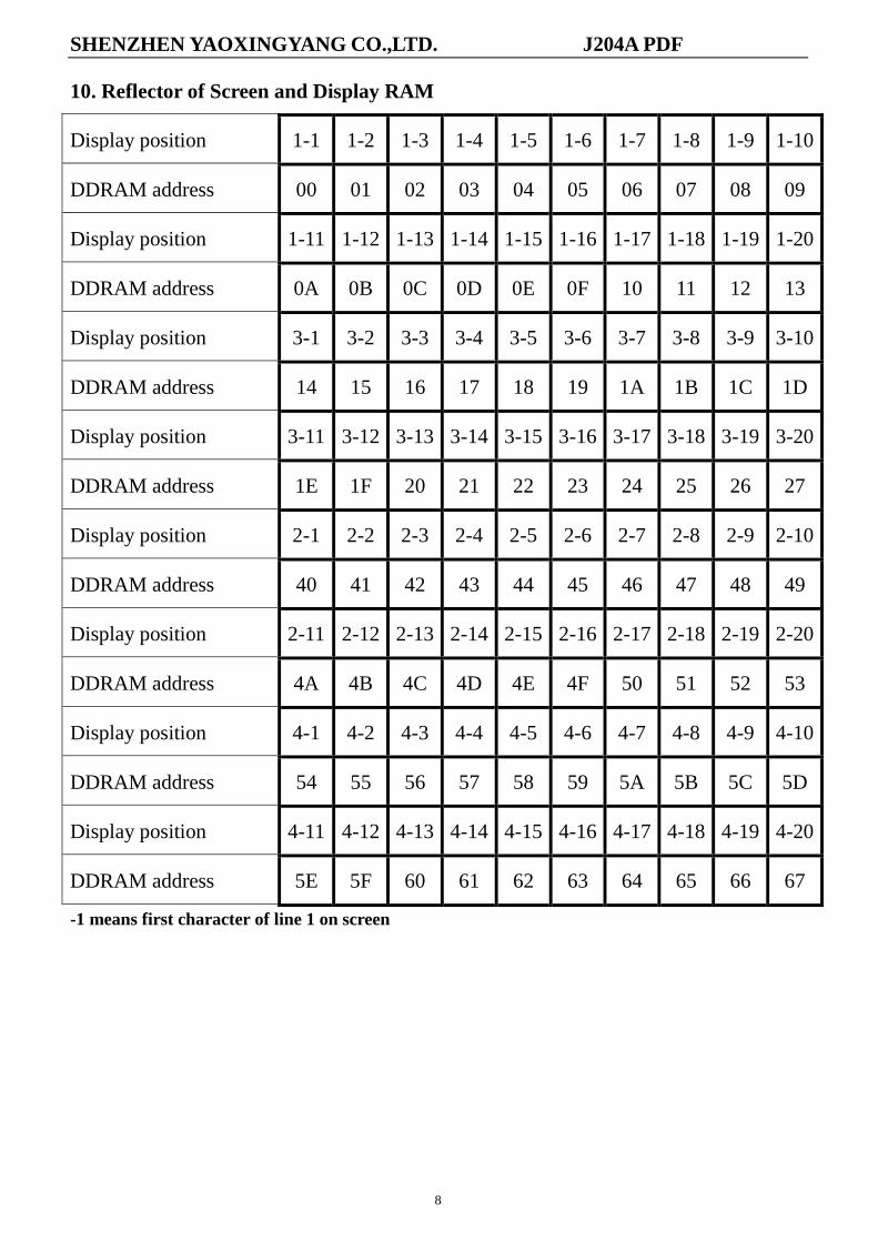
10. Reflector of Screen and Display RAM
Display position 1-1 1-2 1-3 1-4 1-5 1-6 1-7 1-8 1-9 1-10
DDRAM address 00 01 02 03 04 05 06 07 08 09
Display position 1-11 1-12 1-13 1-14 1-15 1-16 1-17 1-18 1-19 1-20
DDRAM address 0A 0B 0C 0D 0E 0F 10 11 12 13
Display position 3-1 3-2 3-3 3-4 3-5 3-6 3-7 3-8 3-9 3-10
DDRAM address 14 15 16 17 18 19 1A 1B 1C 1D
Display position 3-11 3-12 3-13 3-14 3-15 3-16 3-17 3-18 3-19 3-20
DDRAM address 1E 1F 20 21 22 23 24 25 26 27
Display position 2-1 2-2 2-3 2-4 2-5 2-6 2-7 2-8 2-9 2-10
DDRAM address 40 41 42 43 44 45 46 47 48 49
Display position 2-11 2-12 2-13 2-14 2-15 2-16 2-17 2-18 2-19 2-20
DDRAM address 4A 4B 4C 4D 4E 4F 50 51 52 53
Display position 4-1 4-2 4-3 4-4 4-5 4-6 4-7 4-8 4-9 4-10
DDRAM address 54 55 56 57 58 59 5A 5B 5C 5D
Display position 4-11 4-12 4-13 4-14 4-15 4-16 4-17 4-18 4-19 4-20
DDRAM address 5E 5F 60 61 62 63 64 65 66 67
-1 means first character of line 1 on screen

SHENZHEN YAOXINGYANG CO.,LTD. J204A PDF
9
11. DISPLAY CONTROL INSTRUCTION Instruction Code Instruction
RS R/W DB7 DB6 DB5 DB4 DB3 DB2 DB1 DB0
Description ExecutionTime(f
osc=270kHz)
Clear
Display
0 0 0 0 0 0 0 0 0 1 Write “20H” to DDRAM set
DDRAM address to “00H” from AC
1.52ms
Return
Home
0 0 0 0 0 0 0 0 1 - Set DDRAM address to “00H” from
AC and return cursor to its original
position if shifted. The contents of
DDRAM are not changed
1.52ms
Entry Mode
Set
0 0 0 0 0 0 0 1 I/D SH Assign cursor moving direction and
enable the shift of entire display
38μs
Display
ON/OFF
Control
0 0 0 0 0 0 1 D C B Set display (D) cursor(C) and
blinking of cursor(B) on/off
38μs
Cursor or
Display
Shift
0 0 0 0 0 1 S/C R/L - - Set cursor moving and display shift
control bit, and the direction, without
changing DDRAM data
38μs
Function Set 0 0 0 0 1 DL N F - - Set interface data length of display
line (N: 2line/1line)and, display font
type F:5X11dots/5X8dots
38μs
Set CGRAM
Address
0 0 0 1 AC5 AC4 AC3 AC2 AC1 AC0 Set CGRAM address in address
counter
38μs
Set
DDRAM
Address
0 0 1 AC6 AC5 AC4 AC3 AC2 AC1 AC0 Set DDRAM address in address
counter
38μs
Read Busy
Flag and
Address
0 1 BF AC6 AC5 AC4 AC3 AC2 AC1 AC0 Whether during internal operation or
not can be known by reading BF The
contents of address counter of
address counter can also be read
0μs
Write Data
to RAM
1 0 D7 D6 D5 D4 D3 D2 D1 D0 Write data into internal RAM
(DDRAM/CGRAM)
38μs
Read data
from RAM
1 1 D7 D6 D5 D4 D3 D2 D1 D0 Read data from internal RAM
(DDRAM/CGRAM)
38μs
Instruction Description
Clear Display RS R/W DB7 DB6 DB5 DB4 DB3 DB2 DB1 DB0 0 0 0 0 0 0 0 0 0 1
Clear all the display data by writing “20H” (space code) to all DDRAM address, and set DDRAM address to “00H” into AC(address counter).Return cursor to the original status, namely, bring the cursor to the left edge on the first line of the display. Make the entry mode increment(I/D=HIGH) Return Home
RS R/W DB7 DB6 DB5 DB4 DB3 DB2 DB1 DB0 0 0 0 0 0 0 0 0 1 -
Set DDRAM address to “00H” into the address counter. Return cursor to its original site and return display to its original status, if shifted. Contents of DDRAM do not change.

SHENZHEN YAOXINGYANG CO.,LTD. J204A PDF
10
Entry Mode Set RS R/W DB7 DB6 DB5 DB4 DB3 DB2 DB1 DB0 0 0 0 0 0 0 0 1 I/D SH
Set the moving direction of cursor and display. I/D: Increment/decrement of DDRAM address (cursor or blink) When I/D=High, cursor/blink moves to right and DDRAM address is increased by 1. When I/D=low, cursor/blink moves to left and DDRAM address is decreased by 1. *CGRAM operates the same as DDRAM, when reading from or writing to CGRAM. SH: Shift of entire display When DDRAM read (CGRAM read/write) operation or SH=”Low”, shifting of entire display is not performed. If SH=High, and DDRAM write operation, shift of entire display is performed according to I/D value(I/D=High, shift left, I/D=Low, shift right). Display ON/OFF Control
RS R/W DB7 DB6 DB5 DB4 DB3 DB2 DB1 DB0 0 0 0 0 0 0 1 D C B
D: Display ON/OFF control bit When D=High, entire display is turned on. When D=Low, display is turned off, but display data remains in DDRAM. C: Cursor ON/OFF control bit When C=High, cursor is turned on. When C=Low, cursor is disappeared in current display, but I/D register preserves its data. B: Cursor Blink ON/OFF control bit When B=High, cursor blink is on ,which performs alternately between all the high data and display characters at the cursor position. When B=Low, Blink is off. Cursor or Display Shift
RS R/W DB7 DB6 DB5 DB4 DB3 DB2 DB1 DB0 0 0 0 0 0 1 S/C R/L - -
Shifting of right/left cursor position or display without writing or reading of display data. This instruction is used to correct or search display data. During 2-line mode display ,cursor moves to the 2nd line after the 40th digit of the 1st line. Note that display shift is performed simultaneously in all the lines. When displayed data is shifted repeatedly, each line is shifted individually. When display shift is performed, the contents of the address counter are not changed.
S/C R/L Operation 0 0 Shift cursor to the left, AC is decreased by 1 0 1 Shift cursor to the right, AC is increased by 1 1 0 Shift all the display to the left, Cursor moves according to the display 1 1 Shift all the display to the right, cursor moves according to the display
Function set
RS R/W DB7 DB6 DB5 DB4 DB3 DB2 DB1 DB0 0 0 0 0 1 DL N F - -
DL: Interface data length control bit When DL=High, it means 8-bit bus mode with MPU. When DL=Low, it means 4-bit bus mode with MPU. When 4-bit bus mode, it needs to transfer 4-bit data twice. N: Display line number control bit When N=Low, 1-line display mode is set.
SHENZHEN YAOXINGYANG CO.,LTD. J204A PDF
11
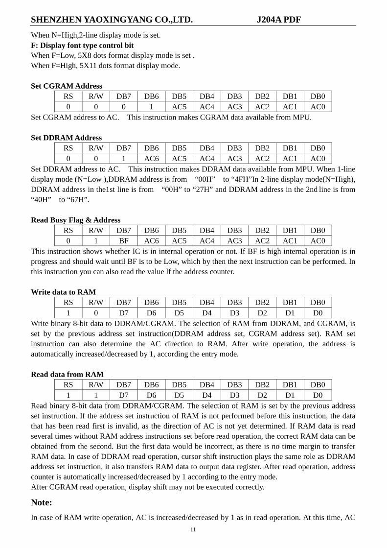
When N=High,2-line display mode is set. F: Display font type control bit When F=Low, 5X8 dots format display mode is set . When F=High, 5X11 dots format display mode. Set CGRAM Address
RS R/W DB7 DB6 DB5 DB4 DB3 DB2 DB1 DB0 0 0 0 1 AC5 AC4 AC3 AC2 AC1 AC0
Set CGRAM address to AC. This instruction makes CGRAM data available from MPU. Set DDRAM Address
RS R/W DB7 DB6 DB5 DB4 DB3 DB2 DB1 DB0 0 0 1 AC6 AC5 AC4 AC3 AC2 AC1 AC0
Set DDRAM address to AC. This instruction makes DDRAM data available from MPU. When 1-line display mode (N=Low ),DDRAM address is from “00H” to “4FH”In 2-line display mode(N=High), DDRAM address in the1st line is from “00H” to “27H” and DDRAM address in the 2nd line is from “40H” to “67H”. Read Busy Flag & Address
RS R/W DB7 DB6 DB5 DB4 DB3 DB2 DB1 DB0 0 1 BF AC6 AC5 AC4 AC3 AC2 AC1 AC0
This instruction shows whether IC is in internal operation or not. If BF is high internal operation is in progress and should wait until BF is to be Low, which by then the next instruction can be performed. In this instruction you can also read the value lf the address counter. Write data to RAM
RS R/W DB7 DB6 DB5 DB4 DB3 DB2 DB1 DB0 1 0 D7 D6 D5 D4 D3 D2 D1 D0
Write binary 8-bit data to DDRAM/CGRAM. The selection of RAM from DDRAM, and CGRAM, is set by the previous address set instruction(DDRAM address set, CGRAM address set). RAM set instruction can also determine the AC direction to RAM. After write operation, the address is automatically increased/decreased by 1, according the entry mode. Read data from RAM
RS R/W DB7 DB6 DB5 DB4 DB3 DB2 DB1 DB0 1 1 D7 D6 D5 D4 D3 D2 D1 D0
Read binary 8-bit data from DDRAM/CGRAM. The selection of RAM is set by the previous address set instruction. If the address set instruction of RAM is not performed before this instruction, the data that has been read first is invalid, as the direction of AC is not yet determined. If RAM data is read several times without RAM address instructions set before read operation, the correct RAM data can be obtained from the second. But the first data would be incorrect, as there is no time margin to transfer RAM data. In case of DDRAM read operation, cursor shift instruction plays the same role as DDRAM address set instruction, it also transfers RAM data to output data register. After read operation, address counter is automatically increased/decreased by 1 according to the entry mode. After CGRAM read operation, display shift may not be executed correctly.
Note:
In case of RAM write operation, AC is increased/decreased by 1 as in read operation. At this time, AC

SHENZHEN YAOXINGYANG CO.,LTD. J204A PDF
12
indicates the next address position, but only the previous data can be read by the read instruction.
Relationship between Character Code and CGRAM
Character code CGRAM Address CGRAM Data Pattern number D7 D6 D5 D4 D3 D2 D1 D0 A5 A4 A3 A2 A1 A0 P7 P6 P5 P4 P3 P2 P1 P0 0 0 0 0 x 0 0 0 0 0 0 0 0 0
0 0 1 0 1 0 0 1 1 1 0 0 1 0 1 1 1 0 1 1 1
x x x 0 1 1 1 0 x x x 1 0 0 0 0 x x x 1 0 0 0 0 x x x 0 1 1 1 0 x x x 0 0 0 0 1 x x x 0 0 0 0 1 x x x 0 1 1 1 0 x x x 0 0 0 0 0
Pattern1
0 0 0 0 x 1 1 1 0 0 0 0 0 0 0 0 1 0 1 0 0 1 1 1 0 0 1 0 1 1 1 0 1 1 1
x x x 0 1 1 1 0 x x x 1 0 0 0 1 x x x 1 0 0 0 1 x x x 1 1 1 1 1 x x x 1 0 0 0 1 x x x 1 0 0 0 1 x x x 1 0 0 0 1 x x x 0 0 0 0 0
Pattern8
Display Data RAM(DDRAM)
DDRAM stores display data of maximum 80x8bits (80 characters). DDRAM address is set in the address counter (AC) as a hexadecimal number
MSB LSB
AC6 AC5 AC4 AC3 AC2 AC1 AC0
SHENZHEN YAOXINGYANG CO.,LTD. J204A PDF
13
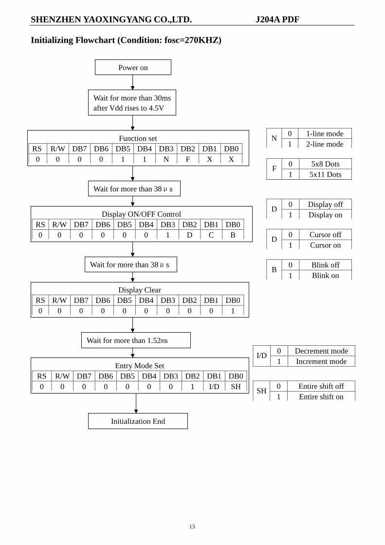
Initializing Flowchart (Condition: fosc=270KHZ)
Power on
Wait for more than 30ms after Vdd rises to 4.5V
Function set RS R/W DB7 DB6 DB5 DB4 DB3 DB2 DB1 DB0 0 0 0 0 1 1 N F X X
Wait for more than 38μs
Display ON/OFF Control RS R/W DB7 DB6 DB5 DB4 DB3 DB2 DB1 DB0 0 0 0 0 0 0 1 D C B
Wait for more than 38μs
Display Clear RS R/W DB7 DB6 DB5 DB4 DB3 DB2 DB1 DB0 0 0 0 0 0 0 0 0 0 1
Wait for more than 1.52ms
Entry Mode Set RS R/W DB7 DB6 DB5 DB4 DB3 DB2 DB1 DB0 0 0 0 0 0 0 0 1 I/D SH
Initialization End
0 1-line mode N
1 2-line mode
0 5x8 Dots F
1 5x11 Dots
0 Display off D
1 Display on
0 Cursor off D
1 Cursor on
0 Blink off B
1 Blink on
0 Decrement mode I/D
1 Increment mode
0 Entire shift off SH
1 Entire shift on
SHENZHEN YAOXINGYANG CO.,LTD. J204A PDF
14
ΦΦ
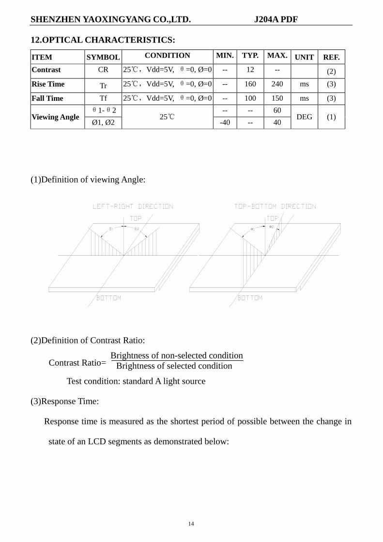
12.OPTICAL CHARACTERISTICS:
ITEM SYMBOL CONDITION MIN. TYP. MAX. UNIT REF.
Contrast CR 25℃,Vdd=5V, θ=0, Ø=0 -- 12 -- (2)
Rise Time Tr 25℃,Vdd=5V, θ=0, Ø=0 -- 160 240 ms (3)
Fall Time Tf 25℃,Vdd=5V, θ=0, Ø=0 -- 100 150 ms (3)
θ1-θ2 -- -- 60 Viewing Angle
Ø1, Ø2 25℃
-40 -- 40 DEG (1)
(1)Definition of viewing Angle:
(2)Definition of Contrast Ratio:
Brightness of non-selected condition Brightness of selected condition
Test condition: standard A light source
(3)Response Time:
Response time is measured as the shortest period of possible between the change in
state of an LCD segments as demonstrated below:
Contrast Ratio=

SHENZHEN YAOXINGYANG CO.,LTD. J204A PDF
15
0
Brig
htne
ss
90%
10%
Tr Tf
V
T
T
13.POWER SUPPLY SCHEMATICS
VR(VR=20K)
For Single Source
DOT
Mtri
xLC
D Mo
dule
+5V
VDD
SSV
OV
DOT Mt
rix
LCD
Module
(VR=20K)
OV
DDV
VSS
RV
Vee
+5V
For Double Source
-5V to -10V
SHENZHEN YAOXINGYANG CO.,LTD. J204A PDF
16
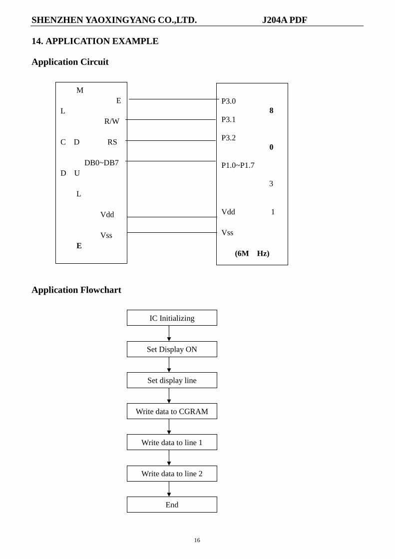
14. APPLICATION EXAMPLE
Application Circuit
Application Flowchart
M E
L R/W C D RS
DB0~DB7 D U
L Vdd
Vss E
P3.0
8 P3.1 P3.2
0
P1.0~P1.7 3 Vdd 1 Vss
(6M Hz)
IC Initializing
Set Display ON
Set display line
Write data to CGRAM
Write data to line 1
Write data to line 2
End
SHENZHEN YAOXINGYANG CO.,LTD. J204A PDF
17

SHENZHEN YAOXINGYANG CO.,LTD. J204A PDF
18
15. PRECAUTION FOR USING LCM
1. Liquid Crystal Display (LCD) LCD is made up of glass, organic sealant, organic fluid, and polymer based polarizers. The following precautions should be taken when handing, (1). Keep the temperature within range of use and storage. Excessive temperature and humidity could cause polarization degradation, polarizer peel off or bubble. (2). Do not contact the exposed polarizers with anything harder than an HB pencil lead. To clean dust off the display surface. Wipe gently with cotton. Chamois or other soft material soaked in petroleum benzine. (3). Wipe off saliva or water drops immediately. Contact with water over a long period of time may cause polarizer deformation or color fading, while an active LCD with water condensation on its surface will cause corrosion of ITO electrodes. (4). Glass can be easily chipped or cracked from rough handing. especially at corners and edges. (5). Do not drive LCD with DC voltage. 2. Liquid Crystal Display Modules 2.1 Mechanical Considerations LCM are assembled and adjusted with a high degree of precision. Avoid excessive shocks and do not make any alterations or modifications. The following should be noted. (1). Do not tamper in any way with the tabs on the tabs on the metal frame. (2). Do not modify the PCB by drilling extra holes, changing its outline, moving its components or modifying its pattern. (3). Do not touch the elastomer connector, especially insert an backlight panel (for example, EL). (4). When mounting a LCM make sure that the PCB is not under any tress such as bending or twisting. Elastomer contacts are very delicate and missing pixels could result from slight dislocation of any of the elements. (5). Avoid pressing on the metal bezel, otherwise the elastomer connector could be deformed and lose contact, resulting in missing pie ls. 2.2. Static Electricity LCM contains CMOS LSI’s and the same precaution for such devices should apply, namely (1). The operator should be grounded whenever he/she comes into contact with the module. Never touch any of the conductive parts such as the LSI pads, the copper leads on the PCB and the interface terminals with any parts of the human body. (2). The modules should be kept in antistatic bags or other containers resistant to static for storage. (3). Only properly grounded soldering irons should be used. (4). If an electric screwdriver is used, it should be well grounded and shielded from commutator sparks. (5). The normal static prevention measures should be observed for work clothes and working benches; for the latter conductive ( rubber) mat is recommended. (6). Since dry air is inductive to static, a relative humidity of 50-60% is recommended. 2.3. Soldering (1). Solder only to the I/O terminals. (2). Use only soldering irons with proper grounding and no leakage. (3). Soldering temperature: 280 ℃±10℃ (4). Soldering time: 3 to 4 sec. (5). Use eutectic solder with resin flux fill. (6). If flux is used, the LCD surface should be covered to avoid flux spatters. Flux residue should be removed after wards. 2.4. Operation (1). The viewing angle can be adjusted by varying the LCD driving voltage V0. (2). Driving voltage should be kept within specified range; excess voltage shortens display life. (3). Response time increases with decrease in temperature. (4). Display may turn black or dark blue at temperatures above its operational range; this is (however not pressing on the viewing area) may cause the segments to appear “fractured”.
SHENZHEN YAOXINGYANG CO.,LTD. J204A PDF
19
(5). Mechanical disturbance during operation (such as pressing on the viewing area) nay cause the segments to appear “fractured”. 2.5. Storage If any fluid leaks out of a damaged glass cell, wash off any human part that comes into contact with soap and water. Never swallow the fluid. The toxicity is extremely low but caution should be exercised at all the time. 2.6. Limited Warranty Unless otherwise agreed between SHEN ZHEN BLUE MOON CO.,LTD. and customer, SHEN ZHEN BLUE MOON CO.,LTD. will repair or repair any of its LCD and IC, which is found to be defective electrically and visually when inspected in accordance with SHEN ZHEN BLUE MOON CO.,LTD. acceptance standards, for a period on one year from data of shipment. Confirmation of such date shall be based on freight documents. The warranty liability of SHEN ZHEN BLUE MOON CO.,LTD. is limited to repair and/or replacement on the terms set forth above. SHEN ZHEN BLUE MOON CO.,LTD. will not responsible for any subsequent or consequential events.