SGM48752 CMOS Analog Multiplexercn.sg-micro.com/uploads/soft/20190626/1561545244.pdf · SGM48752...
15
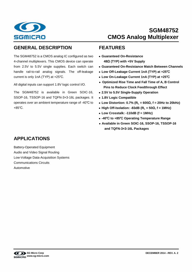
SGM48752 CMOS Analog Multiplexer DECEMBER 2014 –REV. A. 2 SG Micro Corp www.sg-micro.com GENERAL DESCRIPTION The SGM48752 is a CMOS analog IC configured as two 4-channel multiplexers. This CMOS device can operate from 2.5V to 5.5V single supplies. Each switch can handle rail-to-rail analog signals. The off-leakage current is only 1nA (TYP) at +25℃. All digital inputs can support 1.8V logic control I/O. The SGM48752 is available in Green SOIC-16, SSOP-16, TSSOP-16 and TQFN-3×3-16L packages. It operates over an ambient temperature range of -40℃ to +85℃. APPLICATIONS Battery-Operated Equipment Audio and Video Signal Routing Low-Voltage Data-Acquisition Systems Communications Circuits Automotive FEATURES Guaranteed On-Resistance 48Ω (TYP) with +5V Supply Guaranteed On-Resistance Match Between Channels Low Off-Leakage Current 1nA (TYP) at +25℃ Low On-Leakage Current 1nA (TYP) at +25℃ Optimized Rise Time and Fall Time of A, B Control Pins to Reduce Clock Feedthrough Effect 2.5V to 5.5V Single-Supply Operation 1.8V Logic Compatible Low Distortion: 0.7% (R L = 600Ω, f = 20Hz to 20kHz) High Off-Isolation: -83dB (R L = 50Ω, f = 1MHz) Low Crosstalk: -110dB (f = 1MHz) -40℃ to +85℃ Operating Temperature Range Available in Green SOIC-16, SSOP-16, TSSOP-16 and TQFN-3×3-16L Packages
Transcript of SGM48752 CMOS Analog Multiplexercn.sg-micro.com/uploads/soft/20190626/1561545244.pdf · SGM48752...
SGM48752 CMOS Analog Multiplexer
DECEMBER 2014 –REV. A. 2 SG Micro Corp www.sg-micro.com
GENERAL DESCRIPTION The SGM48752 is a CMOS analog IC configured as two 4-channel multiplexers. This CMOS device can operate from 2.5V to 5.5V single supplies. Each switch can handle rail-to-rail analog signals. The off-leakage current is only 1nA (TYP) at +25.
All digital inputs can support 1.8V logic control I/O.
The SGM48752 is available in Green SOIC-16, SSOP-16, TSSOP-16 and TQFN-3×3-16L packages. It operates over an ambient temperature range of -40 to +85.
APPLICATIONS Battery-Operated Equipment Audio and Video Signal Routing Low-Voltage Data-Acquisition Systems Communications Circuits Automotive
FEATURES Guaranteed On-Resistance
48Ω (TYP) with +5V Supply Guaranteed On-Resistance Match Between Channels Low Off-Leakage Current 1nA (TYP) at +25 Low On-Leakage Current 1nA (TYP) at +25 Optimized Rise Time and Fall Time of A, B Control
Pins to Reduce Clock Feedthrough Effect 2.5V to 5.5V Single-Supply Operation 1.8V Logic Compatible Low Distortion: 0.7% (RL = 600Ω, f = 20Hz to 20kHz) High Off-Isolation: -83dB (RL = 50Ω, f = 1MHz) Low Crosstalk: -110dB (f = 1MHz) -40 to +85 Operating Temperature Range Available in Green SOIC-16, SSOP-16, TSSOP-16
and TQFN-3×3-16L Packages
SGM48752 CMOS Analog Multiplexer
2
DECEMBER 2014 SG Micro Corp www.sg-micro.com
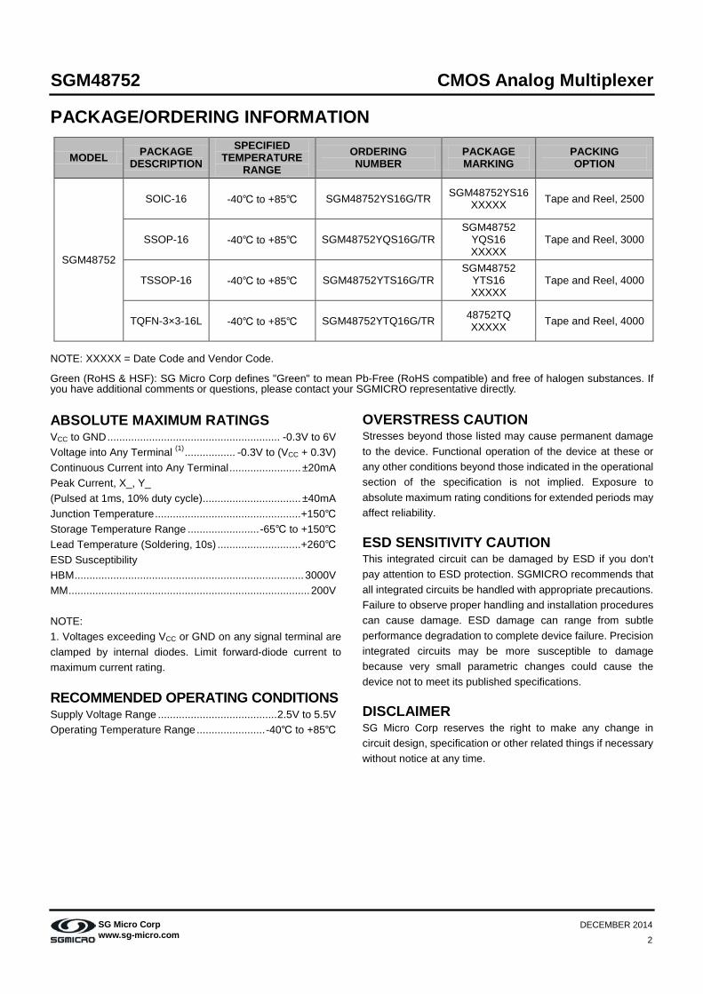
PACKAGE/ORDERING INFORMATION
MODEL PACKAGE DESCRIPTION
SPECIFIED TEMPERATURE
RANGE ORDERING NUMBER
PACKAGE MARKING
PACKING OPTION
SGM48752
SOIC-16 -40 to +85 SGM48752YS16G/TR SGM48752YS16 XXXXX Tape and Reel, 2500
SSOP-16 -40 to +85 SGM48752YQS16G/TR SGM48752
YQS16 XXXXX
Tape and Reel, 3000
TSSOP-16 -40 to +85 SGM48752YTS16G/TR SGM48752
YTS16 XXXXX
Tape and Reel, 4000
TQFN-3×3-16L -40 to +85 SGM48752YTQ16G/TR 48752TQ XXXXX Tape and Reel, 4000
NOTE: XXXXX = Date Code and Vendor Code.
Green (RoHS & HSF): SG Micro Corp defines "Green" to mean Pb-Free (RoHS compatible) and free of halogen substances. If you have additional comments or questions, please contact your SGMICRO representative directly. ABSOLUTE MAXIMUM RATINGS VCC to GND .......................................................... -0.3V to 6V Voltage into Any Terminal (1) ................. -0.3V to (VCC + 0.3V) Continuous Current into Any Terminal ........................ ±20mA Peak Current, X_, Y_ (Pulsed at 1ms, 10% duty cycle) ................................. ±40mA Junction Temperature ................................................. +150 Storage Temperature Range ........................ -65 to +150 Lead Temperature (Soldering, 10s) ............................ +260 ESD Susceptibility HBM ............................................................................. 3000V MM ................................................................................. 200V NOTE: 1. Voltages exceeding VCC or GND on any signal terminal are clamped by internal diodes. Limit forward-diode current to maximum current rating. RECOMMENDED OPERATING CONDITIONS Supply Voltage Range ........................................ 2.5V to 5.5V Operating Temperature Range ....................... -40 to +85
OVERSTRESS CAUTION Stresses beyond those listed may cause permanent damage to the device. Functional operation of the device at these or any other conditions beyond those indicated in the operational section of the specification is not implied. Exposure to absolute maximum rating conditions for extended periods may affect reliability. ESD SENSITIVITY CAUTION This integrated circuit can be damaged by ESD if you don’t pay attention to ESD protection. SGMICRO recommends that all integrated circuits be handled with appropriate precautions. Failure to observe proper handling and installation procedures can cause damage. ESD damage can range from subtle performance degradation to complete device failure. Precision integrated circuits may be more susceptible to damage because very small parametric changes could cause the device not to meet its published specifications. DISCLAIMER SG Micro Corp reserves the right to make any change in circuit design, specification or other related things if necessary without notice at any time.

SGM48752 CMOS Analog Multiplexer
3
DECEMBER 2014 SG Micro Corp www.sg-micro.com
PIN CONFIGURATIONS SGM48752 (TOP VIEW) SGM48752 (TOP VIEW)
VCC
Y
X
X0
X1
A
B
Y2
12
13
14
15
161
2
3
4
5Y1
Y0
Y3
6
7
8
11
10
9GND
X3
X2
ENABLE
NCLOGIC
ENABLE
Y1
1
2
3
4
5 7 8
9
10
X3
Y3
X0
Y0
Y
VCC
NC
6
11
12
13141516
GND B A
X1
X
X2Y2
SGM48752
EP
SOIC-16/SSOP-16/TSSOP-16 TQFN-3×3-16L
PIN DESCRIPTION
FUNCTION TABLE
ENABLE INPUT
SELECT INPUTS ON SWITCHES
B A H X X All Switches Open L L L X-X0, Y-Y0 L L H X-X1, Y-Y1 L H L X-X2, Y-Y2 L H H X-X3, Y-Y3
X = Don’t care NOTE: Input and output pins are identical and interchangeable. Either may be considered an input or output; signals pass equally well in either direction.
PIN NAME FUNCTION
SOIC-16/SSOP-16/TSSOP-16 TQFN-3×3-16L 1, 5, 2, 4 15, 3, 16, 2 Y0, Y1, Y2, Y3 Analog Switch “Y” Inputs 0-3.
3 1 Y Analog Switch “Y” Output. 6 4 ENABLE Digital Enable Input. Normally connected to GND. 7 5 NC No Connect. 8 6 GND Ground. Connect to digital ground. 9 7 B Digital Address “B” Input. 10 8 A Digital Address “A” Input.
12, 14, 15, 11 10, 12, 13, 9 X0, X1, X2, X3 Analog Switch “X” Inputs 0-3. 13 11 X Analog Switch “X” Output. 16 14 VCC Positive Analog and Digital Supply Voltage Input. — Exposed Pad EP Exposed Pad. Connect EP to GND.
SGM48752 CMOS Analog Multiplexer
4
DECEMBER 2014 SG Micro Corp www.sg-micro.com
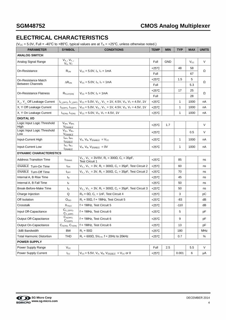
ELECTRICAL CHARACTERISTICS (VCC = 5.0V, Full = -40 to +85, typical values are at TA = +25, unless otherwise noted.)
PARAMETER SYMBOL CONDITIONS TEMP MIN TYP MAX UNITS
ANALOG SWITCH
Analog Signal Range VX_, VY_, VX, VY Full GND VCC V
On-Resistance RON VCC = 5.0V, IX, IY = 1mA +25 48 58
Ω Full 67
On-Resistance Match Between Channels ∆RON VCC = 5.0V, IX, IY = 1mA
+25 1.5 5 Ω
Full 5.3
On-Resistance Flatness RFLAT(ON) VCC = 5.0V, IX = 1mA +25 17 25
Ω Full 28
X_, Y_ Off Leakage Current IX_(OFF), IY_(OFF) VCC = 5.0V, VX_, VY_ = 1V, 4.5V, VX, VY = 4.5V, 1V +25 1 1000 nA
X, Y Off Leakage Current IX(OFF), IY(OFF) VCC = 5.0V, VX_, VY_ = 1V, 4.5V, VX, VY = 4.5V, 1V +25 1 1000 nA
X, Y On Leakage Current IX(ON), IY(ON) VCC = 5.0V, VX, VY = 4.5V, 1V +25 1 1000 nA
DIGITAL I/O Logic Input Logic Threshold High
VAH, VBH, VENABLE +25 1.7 V
Logic Input Logic Threshold Low
VAL, VBL, VENABLE
+25 0.5 V
Input-Current High IAH, IBH, IENABLE
VA, VB, VENABLE = VCC +25 1 1000 nA
Input-Current Low IAL, IBL,
IENABLE VA, VB, VENABLE = 0V +25 1 1000 nA
DYNAMIC CHARACTERISTICS
Address Transition Time tTRANS VX_, VY_ = 3V/0V, RL = 300Ω, CL = 35pF, Test Circuit 1 +25 85 ns
ENABLE Turn-On Time tON VX_, VY_ = 3V, RL = 300Ω, CL = 35pF, Test Circuit 2 +25 60 ns
ENABLE Turn-Off Time tOFF VX_, VY_ = 3V, RL = 300Ω, CL = 35pF, Test Circuit 2 +25 70 ns
Internal A, B Rise Time tR +25 45 ns
Internal A, B Fall Time tF +25 50 ns
Break-Before-Make Time tD VX_, VY_ = 3V, RL = 300Ω, CL = 35pF, Test Circuit 3 +25 50 ns
Charge Injection Q RS = 0Ω, CL = 1nF, Test Circuit 4 +25 3 pC
Off Isolation OISO RL = 50Ω, f = 1MHz, Test Circuit 5 +25 -83 dB
Crosstalk XTALK f = 1MHz, Test Circuit 5 +25 -110 dB
Input Off-Capacitance CX_(OFF), CY_(OFF)
f = 1MHz, Test Circuit 6 +25 5 pF
Output Off-Capacitance CX(OFF), CY(OFF)
f = 1MHz, Test Circuit 6 +25 9 pF
Output On-Capacitance CX(ON), CY(ON) f = 1MHz, Test Circuit 6 +25 13 pF
-3dB Bandwidth BW RL = 50Ω +25 180 MHz
Total Harmonic Distortion THD RL = 600Ω, 5VP-P, f = 20Hz to 20kHz +25 0.7 %
POWER SUPPLY
Power Supply Range VCC Full 2.5 5.5 V
Power Supply Current ICC VCC = 5.5V, VA, VB, VENABLE = VCC or 0 +25 0.001 6 μA
SGM48752 CMOS Analog Multiplexer
5
DECEMBER 2014 SG Micro Corp www.sg-micro.com
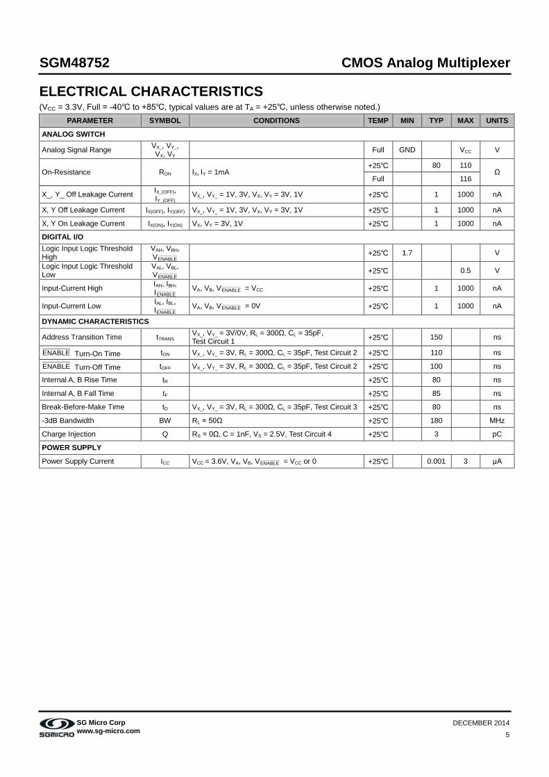
ELECTRICAL CHARACTERISTICS (VCC = 3.3V, Full = -40 to +85, typical values are at TA = +25, unless otherwise noted.)
PARAMETER SYMBOL CONDITIONS TEMP MIN TYP MAX UNITS
ANALOG SWITCH
Analog Signal Range VX_, VY_, VX, VY Full GND VCC V
On-Resistance RON IX, IY = 1mA +25 80 110
Ω Full 116
X_, Y_ Off Leakage Current IX_(OFF), IY_(OFF)
VX_, VY_ = 1V, 3V, VX, VY = 3V, 1V +25 1 1000 nA
X, Y Off Leakage Current IX(OFF), IY(OFF) VX_, VY_ = 1V, 3V, VX, VY = 3V, 1V +25 1 1000 nA
X, Y On Leakage Current IX(ON), IY(ON) VX, VY = 3V, 1V +25 1 1000 nA
DIGITAL I/O Logic Input Logic Threshold High
VAH, VBH, VENABLE +25 1.7 V
Logic Input Logic Threshold Low
VAL, VBL, VENABLE +25 0.5 V
Input-Current High IAH, IBH,
IENABLE VA, VB, VENABLE = VCC +25 1 1000 nA
Input-Current Low IAL, IBL, IENABLE VA, VB, VENABLE = 0V +25 1 1000 nA
DYNAMIC CHARACTERISTICS
Address Transition Time tTRANS VX_, VY_ = 3V/0V, RL = 300Ω, CL = 35pF, Test Circuit 1 +25 150 ns
ENABLE Turn-On Time tON VX_, VY_ = 3V, RL = 300Ω, CL = 35pF, Test Circuit 2 +25 110 ns
ENABLE Turn-Off Time tOFF VX_, VY_ = 3V, RL = 300Ω, CL = 35pF, Test Circuit 2 +25 100 ns
Internal A, B Rise Time tR +25 80 ns
Internal A, B Fall Time tF +25 85 ns
Break-Before-Make Time tD VX_, VY_ = 3V, RL = 300Ω, CL = 35pF, Test Circuit 3 +25 80 ns
-3dB Bandwidth BW RL = 50Ω +25 180 MHz
Charge Injection Q RS = 0Ω, C = 1nF, VS = 2.5V, Test Circuit 4 +25 3 pC
POWER SUPPLY
Power Supply Current ICC VCC = 3.6V, VA, VB, VENABLE = VCC or 0 +25 0.001 3 μA
SGM48752 CMOS Analog Multiplexer
6
DECEMBER 2014 SG Micro Corp www.sg-micro.com
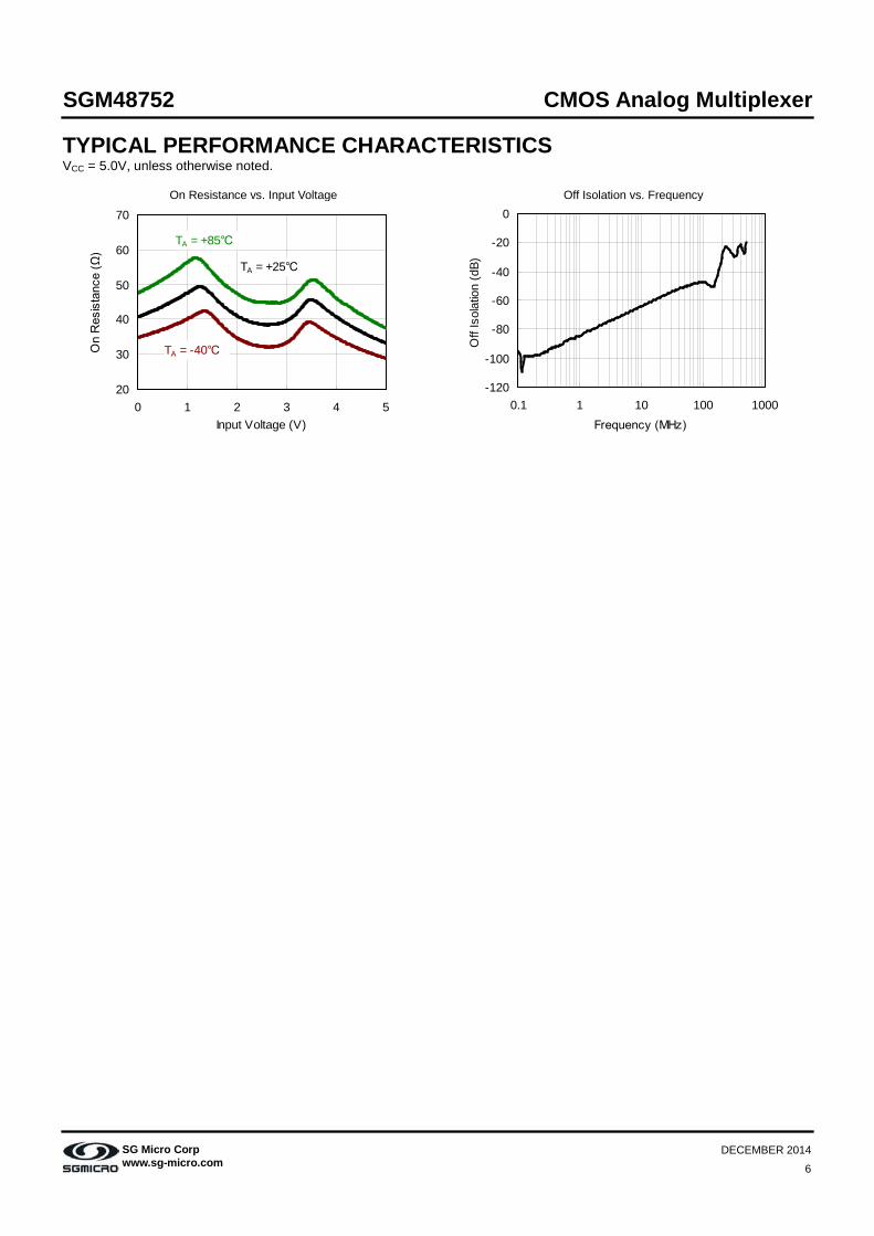
TYPICAL PERFORMANCE CHARACTERISTICS VCC = 5.0V, unless otherwise noted.
On Resistance vs. Input Voltage Off Isolation vs. Frequency
20
30
40
50
60
70
0 1 2 3 4 5Input Voltage (V)
On
Res
ista
nce
(Ω)
TA = +25
TA = -40
TA = +85
-120
-100
-80
-60
-40
-20
0
0.1 1 10 100 1000Frequency (MHz)
Off
Isol
atio
n (d
B)
SGM48752 CMOS Analog Multiplexer
7
DECEMBER 2014 SG Micro Corp www.sg-micro.com
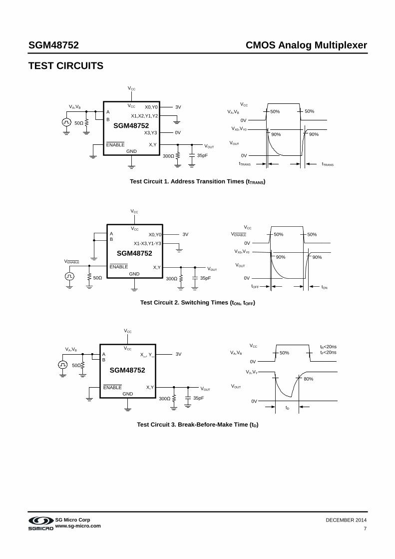
TEST CIRCUITS
35pF
X1,X2,Y1,Y2
GND
0V
300Ω
VOUT
A
ENABLE
X3,Y3
X,Y
3VVA,VB
50Ω
VCC
VCC
SGM48752B
X0,Y0VA,VB
VCC
50%
90%
0V
0V
VOUT
VX0,VY0
90%
tTRANS tTRANS
50%
Test Circuit 1. Address Transition Times (tTRANS)
35pF
X0,Y0
GND
3V
300Ω
VOUT
AB
ENABLE
X1-X3,Y1-Y3
X,YVENABLE
50Ω
VCC
VCC
SGM48752
VENABLE
VCC
50%
90%
0V
VOUT
VX0,VY0
0V
90%
tONtOFF
50%
Test Circuit 2. Switching Times (tON, tOFF)
35pF
X_, Y_
GND
3V
300Ω
VOUT
AB
ENABLE X,Y
VA,VB
50Ω
VCC
VCC
SGM48752
VA,VB
VCC
50%
0V
0V
VOUT
VX,VY
80%
tD
tR<20nstF<20ns
Test Circuit 3. Break-Before-Make Time (tD)
SGM48752 CMOS Analog Multiplexer
8
DECEMBER 2014 SG Micro Corp www.sg-micro.com
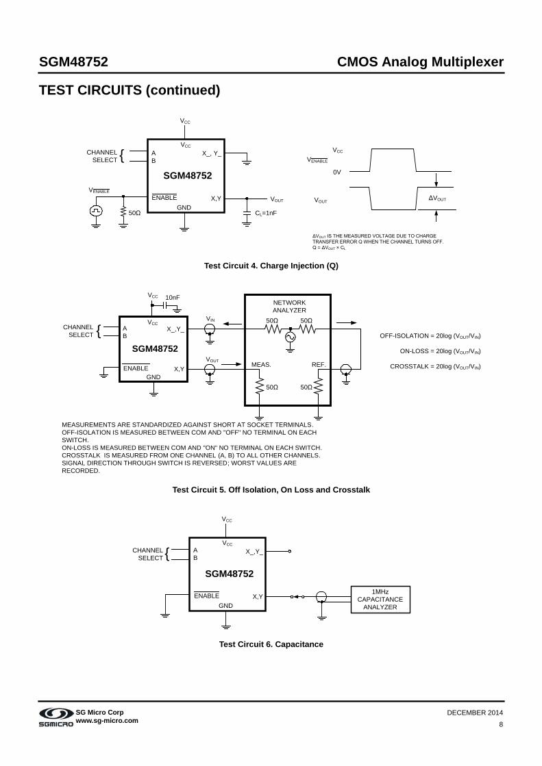
TEST CIRCUITS (continued)
CL=1nF
X_, Y_
GNDVOUT
AB VENABLE
VCC
0V
VOUTENABLE X,Y
VENABLE
50Ω
VCC
VCC
SGM48752
CHANNELSELECT
ΔVOUT
ΔVOUT IS THE MEASURED VOLTAGE DUE TO CHARGETRANSFER ERROR Q WHEN THE CHANNEL TURNS OFF.Q = ΔVOUT × CL
Test Circuit 4. Charge Injection (Q)
X_,Y_
GND
AB
ENABLE X,Y
50Ω
VCC
VCC
SGM48752
CHANNELSELECT
10nF
50Ω
VIN
VOUTMEAS. REF.
50Ω50Ω
NETWORKANALYZER
OFF-ISOLATION = 20log (VOUT/VIN)
ON-LOSS = 20log (VOUT/VIN)
CROSSTALK = 20log (VOUT/VIN)
MEASUREMENTS ARE STANDARDIZED AGAINST SHORT AT SOCKET TERMINALS.OFF-ISOLATION IS MEASURED BETWEEN COM AND "OFF" NO TERMINAL ON EACH SWITCH.ON-LOSS IS MEASURED BETWEEN COM AND "ON" NO TERMINAL ON EACH SWITCH.CROSSTALK IS MEASURED FROM ONE CHANNEL (A, B) TO ALL OTHER CHANNELS.SIGNAL DIRECTION THROUGH SWITCH IS REVERSED; WORST VALUES ARE RECORDED.
Test Circuit 5. Off Isolation, On Loss and Crosstalk
X_,Y_
GND
AB
ENABLE X,Y
VCC
VCC
SGM48752
CHANNELSELECT
1MHzCAPACITANCE
ANALYZER
Test Circuit 6. Capacitance

SGM48752 CMOS Analog Multiplexer
9
DECEMBER 2014 SG Micro Corp www.sg-micro.com
APPLICATION INFORMATION Power-Supply Considerations Overview The SGM48752 construction is typical of most CMOS analog switch. It supports single power supply. VCC and GND are used to drive the internal CMOS switches and set the limits of the analog voltage on any switch. Reverse ESD protection diodes are internally connected between each analog-signal pin and both VCC and GND. If any analog signal exceeds VCC or GND, one of these diodes will conduct. During normal operation, these and other reverse-biased ESD diodes leak, forming the only current drawn from VCC or GND. Virtually all the analog leakage current comes from the ESD diodes. Although the ESD diodes on a given signal pin are identical and therefore fairly well balanced, they are reverse biased differently. Each is biased by either VCC or GND and the analog signal. This means their leakages will vary as the signal varies. The difference in the two diode leakages to the VCC and GND pins constitutes the analog-signal-path leakage current. All analog leakage current flows between each pin and one of the supply terminals, not to the other switch terminal. This is why both sides of a given switch can show leakage currents of either the same or opposite polarity. Over-Voltage Protection Proper power-supply sequencing is recommended for the CMOS device. Do not exceed the absolute maximum ratings because stresses beyond the listed ratings can cause permanent damage to the devices. Always sequence VCC on first, followed by the logic inputs and analog signals. If power-supply sequencing is not possible, add one 100Ω resistor in series with the supply VCC pin for over-voltage protection (Figure 1).
*
VCC
SGM48752 100Ω
*
* *
*INTERNAL PROTECTION DIODES
GND
VCC
0.01μF
X,Y X_,Y_
Figure 1. Over-Voltage Protection Using External Resistor
PACKAGE INFORMATION
TX00012.000 SG Micro Corp www.sg-micro.com
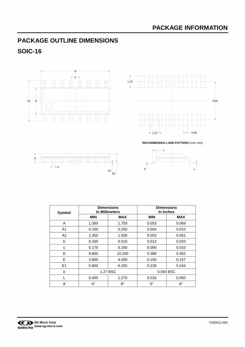
PACKAGE OUTLINE DIMENSIONS SOIC-16
Symbol Dimensions
In Millimeters Dimensions
In Inches MIN MAX MIN MAX
A 1.350 1.750 0.053 0.069 A1 0.100 0.250 0.004 0.010 A2 1.350 1.550 0.053 0.061 b 0.330 0.510 0.013 0.020 c 0.170 0.250 0.006 0.010 D 9.800 10.200 0.386 0.402 E 3.800 4.000 0.150 0.157
E1 5.800 6.200 0.228 0.244 e 1.27 BSC 0.050 BSC L 0.400 1.270 0.016 0.050 θ 0° 8° 0° 8°
D
EE1
e
b
A
A1A2
θ
L
c
RECOMMENDED LAND PATTERN (Unit: mm)
5.60
1.75
1.27 0.65
PACKAGE INFORMATION
TX00026.000 SG Micro Corp www.sg-micro.com
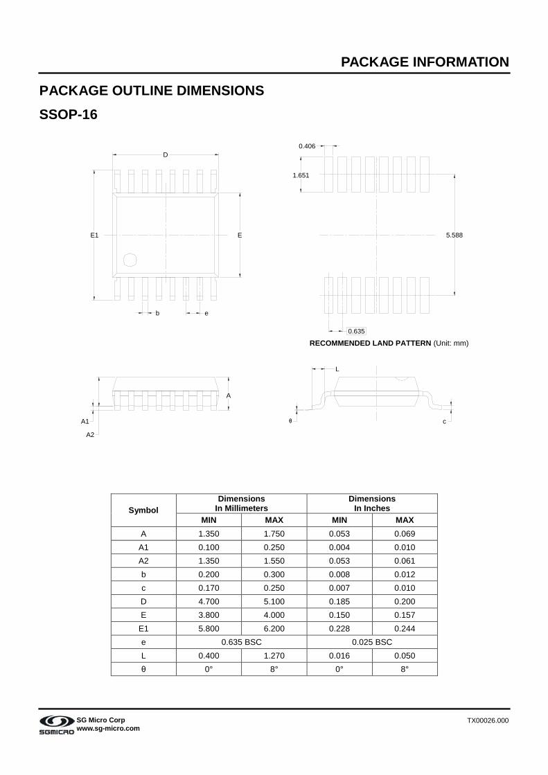
PACKAGE OUTLINE DIMENSIONS SSOP-16
Symbol Dimensions
In Millimeters Dimensions
In Inches MIN MAX MIN MAX
A 1.350 1.750 0.053 0.069 A1 0.100 0.250 0.004 0.010 A2 1.350 1.550 0.053 0.061 b 0.200 0.300 0.008 0.012 c 0.170 0.250 0.007 0.010 D 4.700 5.100 0.185 0.200 E 3.800 4.000 0.150 0.157
E1 5.800 6.200 0.228 0.244 e 0.635 BSC 0.025 BSC L 0.400 1.270 0.016 0.050 θ 0° 8° 0° 8°
EE1
D
A
A1
A2
eb
cθ
L
0.635
0.406
5.588
1.651
RECOMMENDED LAND PATTERN (Unit: mm)

PACKAGE INFORMATION
TX00020.001 SG Micro Corp www.sg-micro.com
PACKAGE OUTLINE DIMENSIONS TSSOP-16
Symbol Dimensions
In Millimeters Dimensions
In Inches MIN MAX MIN MAX
A 1.200 0.047 A1 0.050 0.150 0.002 0.006 A2 0.800 1.050 0.031 0.041 b 0.190 0.300 0.007 0.012 c 0.090 0.200 0.004 0.008 D 4.860 5.100 0.191 0.201 E 4.300 4.500 0.169 0.177
E1 6.200 6.600 0.244 0.260 e 0.650 BSC 0.026 BSC L 0.500 0.700 0.02 0.028 H 0.25 TYP 0.01 TYP θ 1° 7° 1° 7°
E1 E
be
A
A2
A1c
θ
L
H
D
1.78
0.42 0.65
5.94
RECOMMENDED LAND PATTERN (Unit: mm)
PACKAGE INFORMATION
TX00081.000 SG Micro Corp www.sg-micro.com
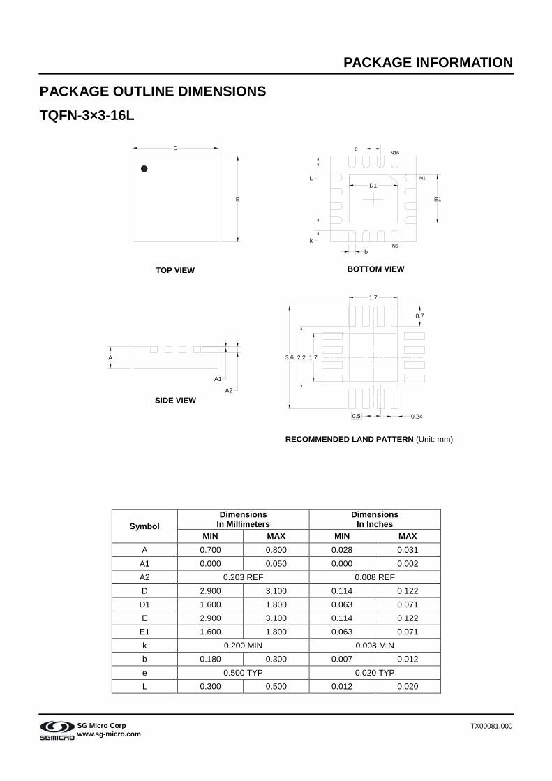
PACKAGE OUTLINE DIMENSIONS TQFN-3×3-16L
Symbol Dimensions
In Millimeters Dimensions
In Inches MIN MAX MIN MAX
A 0.700 0.800 0.028 0.031 A1 0.000 0.050 0.000 0.002 A2 0.203 REF 0.008 REF D 2.900 3.100 0.114 0.122
D1 1.600 1.800 0.063 0.071 E 2.900 3.100 0.114 0.122
E1 1.600 1.800 0.063 0.071 k 0.200 MIN 0.008 MIN b 0.180 0.300 0.007 0.012 e 0.500 TYP 0.020 TYP L 0.300 0.500 0.012 0.020
TOP VIEW BOTTOM VIEW
SIDE VIEW
A
A2
A1
e
E1
b
L
k
D1
D
E
N1
N5
N16
1.7
1.7
0.7
2.23.6
0.5 0.24
RECOMMENDED LAND PATTERN (Unit: mm)
PACKAGE INFORMATION
TX10000.000 SG Micro Corp www.sg-micro.com
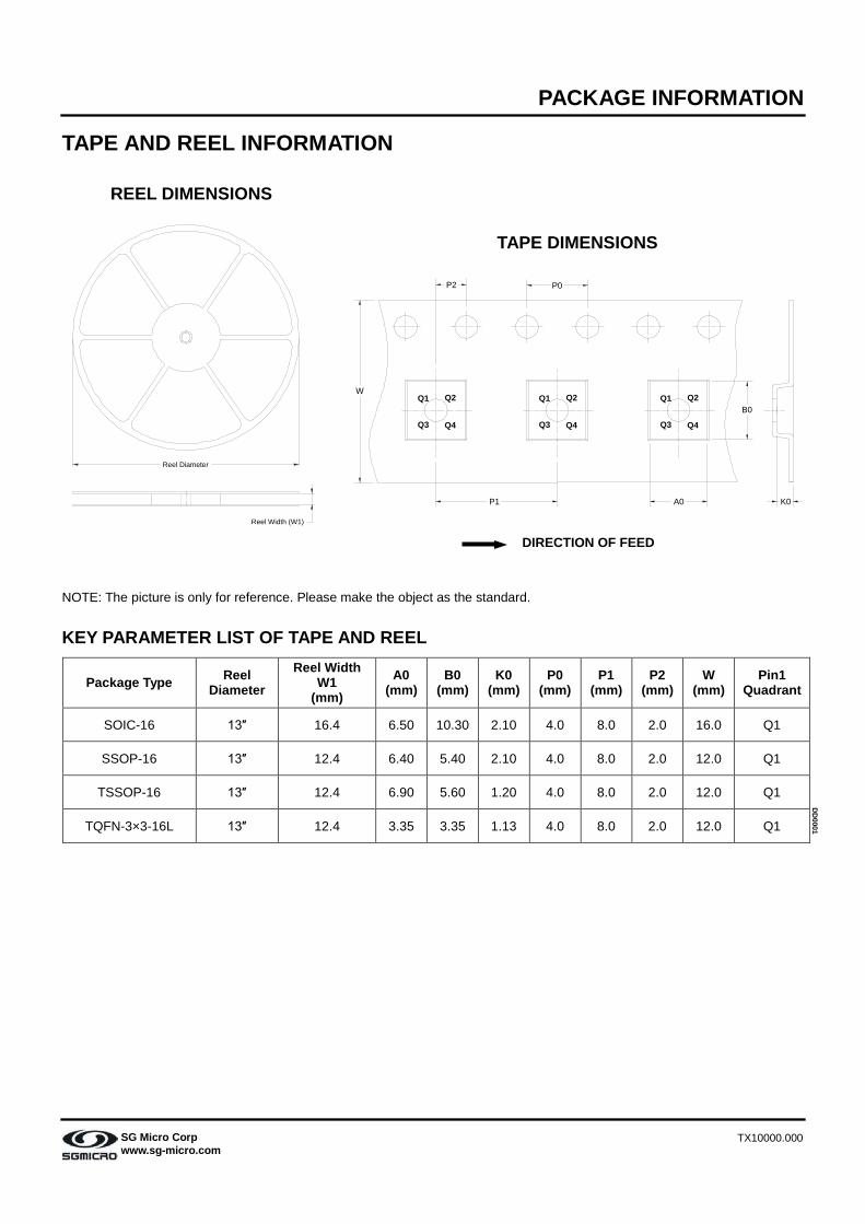
TAPE AND REEL INFORMATION NOTE: The picture is only for reference. Please make the object as the standard.
KEY PARAMETER LIST OF TAPE AND REEL
Package Type Reel Diameter
Reel Width W1
(mm) A0
(mm) B0
(mm) K0
(mm) P0
(mm) P1
(mm) P2
(mm) W
(mm) Pin1
Quadrant
DD
0001
SOIC-16 13″ 16.4 6.50 10.30 2.10 4.0 8.0 2.0 16.0 Q1
SSOP-16 13″ 12.4 6.40 5.40 2.10 4.0 8.0 2.0 12.0 Q1
TSSOP-16 13″ 12.4 6.90 5.60 1.20 4.0 8.0 2.0 12.0 Q1
TQFN-3×3-16L 13″ 12.4 3.35 3.35 1.13 4.0 8.0 2.0 12.0 Q1
Reel Width (W1)
Reel Diameter
REEL DIMENSIONS
TAPE DIMENSIONS
DIRECTION OF FEED
P2 P0
W
P1 A0 K0
B0Q1 Q2
Q4Q3 Q3 Q4
Q2Q1
Q3 Q4
Q2Q1
PACKAGE INFORMATION
TX20000.000 SG Micro Corp www.sg-micro.com
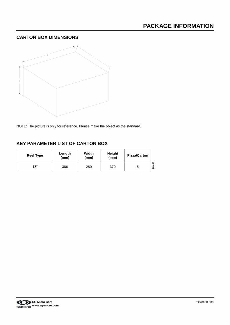
CARTON BOX DIMENSIONS
NOTE: The picture is only for reference. Please make the object as the standard.
KEY PARAMETER LIST OF CARTON BOX
Reel Type Length (mm)
Width (mm)
Height (mm) Pizza/Carton
DD
0002 13″ 386 280 370 5