Seth Jai Parkash Mukandlal Institute Doc: JMIT/ECE-314...
40
1 Seth Jai Parkash Mukandlal Institute of Engg. & Technology, Radaur Doc: JMIT/ECE-314 E Electronics Design Practical Page: Sr. No. Aim of Experiment 1. Design a single stage R C Coupled amplifier and plot its gain frequency response. 2. Design a two stage R C Coupled amplifier and plot its gain frequency response. 3. Design a R C Phase shift oscillator using IC 741.i 4. Design a Wein bridge oscillator. 5. Design a square wave generator using IC 555. 6. Design a 4 : 1 multiplexer and 1 : 4 demultiplexer using logic gates. 7. Design a parallel parity bit generator using ICs. 8. Design a digital to analog converter using ICs. 9. Design a digital frequency meter (0-999HZ) using IC 555 for monoshot, IC- 7404,7408,7490,7447. 10. Design a controller such that LEDs glow in pairs sequentially using IC 7490 and LEDs. 11. To design a second order high pass butterworth filter. 12. To design active notch filter of frequency 100 Hz. 13. To design UJT relaxation oscillator. 14. To design Schmitt trigger using an Op-amp IC-741. 15. To design a second order low pass butterworth filter.
Transcript of Seth Jai Parkash Mukandlal Institute Doc: JMIT/ECE-314...

1
Seth Jai Parkash Mukandlal Institute
of Engg. & Technology, Radaur
Doc:
JMIT/ECE-314 E
Electronics Design Practical
Page:
Sr. No. Aim of Experiment
1. Design a single stage R C Coupled amplifier and plot its gain frequency response.
2. Design a two stage R C Coupled amplifier and plot its gain frequency response.
3. Design a R C Phase shift oscillator using IC 741.i
4. Design a Wein bridge oscillator.
5. Design a square wave generator using IC 555.
6. Design a 4 : 1 multiplexer and 1 : 4 demultiplexer using logic gates.
7. Design a parallel parity bit generator using ICs.
8. Design a digital to analog converter using ICs.
9. Design a digital frequency meter (0-999HZ) using IC 555 for monoshot, IC-
7404,7408,7490,7447.
10. Design a controller such that LEDs glow in pairs sequentially using IC 7490 and
LEDs.
11. To design a second order high pass butterworth filter.
12. To design active notch filter of frequency 100 Hz.
13. To design UJT relaxation oscillator.
14. To design Schmitt trigger using an Op-amp IC-741.
15. To design a second order low pass butterworth filter.
2
Seth Jai Parkash Mukandlal Institute
of Engg. & Technology, Radaur
Doc:
JMIT/ECE-314 E
Electronics Design Practical
Page:
Experiment No.-1
Aim of Experiment: Design a single stage R C Coupled amplifier & plot its gain
frequency response.
Apparatus: Transistor BC-107 ,Regulated power Supply (0-30V, 1A) ,Function
Generator ,CRO ,Resistors[33KΩ, 3.3KΩ, 330Ω, 1.5KΩ 1KΩ, 2.2KΩ, 4.7KΩ]
Capacitors- 10µF -2No 100µF , Bread Board, Connecting Wires
Theory: The R-C Coupled amplifier provides high gain &wide frequency response. The
emitter lead is common to both input & output circuits and is grounded. The emitter-base
circuit is forward biased. The collector current is controlled by the base current rather
than emitter current. The input signal is applied to base terminal of the transistor and
amplifier output is taken across collector terminal. A very small change in base current
produces a much larger change in collector current. When +VE half-cycle is fed to the
input circuit, it opposes the forward bias of the circuit which causes the collector current
to decrease, it decreases the voltage more –VE. Thus when input cycle varies through a -
VE half-cycle, increases the forward bias of the circuit, which causes the collector current
to increases thus the output signal is common emitter amplifier is in out of phase with the
input signal.

3
Seth Jai Parkash Mukandlal Institute
of Engg. & Technology, Radaur
Doc:
JMIT/ECE-314 E
Electronics Design Practical
Page:
Circuit Diagram:
Procedure:
1. Connect the circuit as shown in circuit diagram
2. Apply the input of 20mV peak-to-peak and 1 KHz frequency using Function
Generator
3. Measure the Output Voltage Vo (p-p) for various load resistors
4. Tabulate the readings in the tabular form.
5. The voltage gain can be calculated by using the expression ,Av= (V0/Vi)

4
Seth Jai Parkash Mukandlal Institute
of Engg. & Technology, Radaur
Doc:
JMIT/ECE-314 E
Electronics Design Practical
Page:
6. For plotting the frequency response the input voltage is kept Constant at 20mV
peak-to-peak and the frequency is varied from 100Hz to 1MHz Using function
generator
7. Note down the value of output voltage for each frequency.
8. All the readings are tabulated and voltage gain in dB is calculated by Using The
expression Av=20 log10 (V0/Vi)
9. A graph is drawn by taking frequency on x-axis and gain in dB on y-axis
On Semi-log graph.
The band width of the amplifier is calculated from the graph
Using the expression,
Bandwidth, BW=f2-f1
Where f1 lower cut-off frequency of R-C Coupled amplifier, and
Where f2 upper cut-off frequency of R-C Coupled amplifier
The bandwidth product of the amplifier is calculated using the
Expression
Gain Bandwidth product=3-dBmidband gain X Bandwidth
Observations:
Input voltage Vi=20mV
LOAD
RESISTANCE(KΩ)
OUTPUT
VOLTAGE (V0)
GAIN
AV=(V0/Vi)
GAIN IN dB
Av=20log10
(V0/Vi)

5
Seth Jai Parkash Mukandlal Institute
of Engg. & Technology, Radaur
Doc:
JMIT/ECE-314 E
Electronics Design Practical
Page:
Frequency Response: Vi=20mv
FREQUENCY(Hz) OUTPUT
VOLTAGE (V0)
GAIN IN dB
Av=20 log10 (V0/Vi)
Model Wave Forms:
Input Waveform :

6
Seth Jai Parkash Mukandlal Institute
of Engg. & Technology, Radaur
Doc:
JMIT/ECE-314 E
Electronics Design Practical
Page:
Output Waveform:
Frequency Response:
Result: The voltage gain and frequency response of the RC coupled amplifier are
obtained. Also gain bandwidth product of the amplifier is calculated

7
Seth Jai Parkash Mukandlal Institute
of Engg. & Technology, Radaur
Doc:
JMIT/ECE-314 E
Electronics Design Practical
Page:
Experiment No.-2
Aim of Experiment: Design a two stage R C coupled amplifier & plot its gain frequency
response
Apparatus:
A two stage RC coupled amplifier circuit assembled on board, two AC millivoltmeter,a
function generator, connecting wires
Theory:
An amplifier is an electronics device that increases the amplitude of weak electrical
signals and produces an enlarged version of the signal supplied at the input .in RC
couple, the resistances and capacitances are used to couple one stage of the amplifier with
the next. the role of each component of the circuit in any of the two stage is same as that
of common emitter transistor amplifier except that the coupling capacitor is used here to
pass the amplified signal from the output of first stage to appear at the input of the second
stage without any DC voltage to reach at the base of the second stage from the first stage.
The blocking of the DC voltage by the coupling capacitor allows only the amplified
signal from the second stage to appear across the load resistance.
Circuit Diagram
8
Seth Jai Parkash Mukandlal Institute
of Engg. & Technology, Radaur
Doc:
JMIT/ECE-314 E
Electronics Design Practical
Page:
Procedure
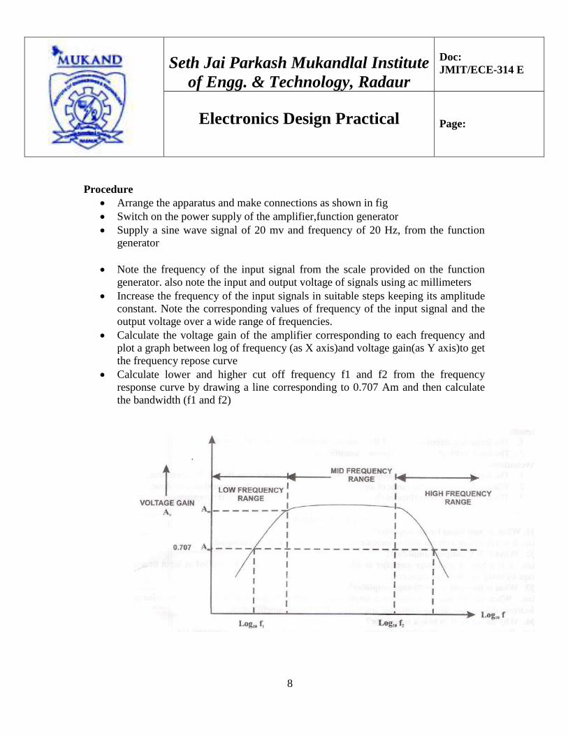
Arrange the apparatus and make connections as shown in fig
Switch on the power supply of the amplifier,function generator
Supply a sine wave signal of 20 mv and frequency of 20 Hz, from the function
generator
Note the frequency of the input signal from the scale provided on the function
generator. also note the input and output voltage of signals using ac millimeters
Increase the frequency of the input signals in suitable steps keeping its amplitude
constant. Note the corresponding values of frequency of the input signal and the
output voltage over a wide range of frequencies.
Calculate the voltage gain of the amplifier corresponding to each frequency and
plot a graph between log of frequency (as X axis)and voltage gain(as Y axis)to get
the frequency repose curve
Calculate lower and higher cut off frequency f1 and f2 from the frequency
response curve by drawing a line corresponding to 0.707 Am and then calculate
the bandwidth (f1 and f2)

9
Seth Jai Parkash Mukandlal Institute
of Engg. & Technology, Radaur
Doc:
JMIT/ECE-314 E
Electronics Design Practical
Page:
Observations Constant input signal voltage, V1=____volt
S. No Frequency of
input signal(Hz)
Log10f Output voltage
Vo
Voltage gain
Av=(Vo/Vi)
1
2
3
4
Calculations
From graph we have log10 f1=___ and log 10 f2=___
f1=___Hz f2=___Hz
The bandwidth of the RC coupled amplifier =f2-f1=___
Result:
The frequency response curve of RC coupled amplifier is plotted
The bandwidth is___
Precautions:
The input voltage of the signal to amplifier should remain constant
The range of the ac mill voltmeter should be properly selected according to the
requirement

10
Seth Jai Parkash Mukandlal Institute
of Engg. & Technology, Radaur
Doc:
JMIT/ECE-314 E
Electronics Design Practical
Page:
Experiment No.-3
Aim of Experiment:- Design a RC phase shift oscillator using IC 741
Apparatus: IC 741, resistances, capacitances, diode (IN4735), Connecting wires.
Theory: In ckt diagram a phase shift oscillator is shown, which consists of op-amp as
amplifying device and three RC cascaded n/ws as feedback ckt. The feedback ckt.
provides feedback voltage from o/p back to the i/p of amplifier. The op-amp is used in
the inverting mode; therefore any signal that appears inv. terminal shifted by 180o at o/p.
An addition 180o phase shift is provided by cascaded RC n/ws so the total phase shift
around the loop is 360o or 0o. At some specific freq. when phase shift of cascade RC
n/ws is exactli 180o and gain of amplifier is sufficiently large ckt. will oscillate at that
freq. of oscillation to
fo = 1/(2(6*R*C)= 0.065/R*C
for producing fo, ckt gain should be 20 and total phase shift is around 360o.
Circuit Diagram:
V0
D1Vz=6.2v
C0.1uF
C0.1uF
C0.1uF
R61M 40%
R535k
R43.3k
R33.3k
R23.3k
R11k
U1IDEAL

11
Seth Jai Parkash Mukandlal Institute
of Engg. & Technology, Radaur
Doc:
JMIT/ECE-314 E
Electronics Design Practical
Page:
Procedure: 1) Connect the ckt. as shown in the fig.
2) Adjust the value of preset and note the waveform at CRO.
3) Measure the freq. of oscillations by observing time period.
Pecautions:
1) Connections should be tight
2) Connections should be checked by instructor before switching on the supply.
Result: We have designed and verified the operation of RC phase shift oscillator.

12
Seth Jai Parkash Mukandlal Institute
of Engg. & Technology, Radaur
Doc:
JMIT/ECE-314 E
Electronics Design Practical
Page:
Experiment No.-4
Aim of Experiment:- To design a Wein bridge oscillator
Apparatus- IC-741, power supply of +15v, -15v, resistances, capacitors, connecting
wires etc.
Theory- A band pass filter has a pass band of two freq. fh and fl such that fh > fl . any
input freq outside this band is attenuated. A band pass filter is said to be narrow band
pass filter if its quality factor Q>10. Thus Q is a measure of selectivity. Measuring higher
value Q, more selective to filter or narrower its bandwidth. The relationship between Q, 3
db bandwidth and center freq fc is given by
Q= fc /BW= fc / (fh –fl)
The filter is unique in two respects.
1. Its has feedback paths.
2. The Op-Amp is used in inverting modes.
R1= Q/(2*Pi* fc *Af) R3= Q/ (Pi* fc *C)
R2=Q/(2*Pi*fc*C*2Q2-Af) Af = R3(R1*R2)
Circuit Diagram:

13
Seth Jai Parkash Mukandlal Institute
of Engg. & Technology, Radaur
Doc:
JMIT/ECE-314 E
Electronics Design Practical
Page:
Procedure- 1.Calculate the values of various ckt. components.
2.Make connections on the bread board.
3.Apply input signal and observe output on CRO.
Result- We have designed Wein Bridge Oscillator.

14
Seth Jai Parkash Mukandlal Institute
of Engg. & Technology, Radaur
Doc:
JMIT/ECE-314 E
Electronics Design Practical
Page:
Experiment No.-5
Aim of Experiment - To design square wave generator using 555 timer IC.
Apparatus: 555 timer IC, Breadboard, diode, Resistor, connecting wires, CRO.
Theory: The stable multivibrator can be used to produce a square wave output simply by
connecting diode ‘D’ across resistors Rb. The capacitor ‘C’ recharge through ‘Ra’ must be
a combination of a fixed resistor & potentiometer so that the potentiometer can be
adjusted for exact square wave.
Circuit Diagram:
15
Seth Jai Parkash Mukandlal Institute
of Engg. & Technology, Radaur
Doc:
JMIT/ECE-314 E
Electronics Design Practical
Page:
Procedure-
1. Connect the ckt. On the breadboard using the diagram shown in fig.
2. Connect the output to be the input of CRO.
3. Observe the waveform on the CRO.
Precautions
1. Connect the components with supply switched off.
2. Observe the output on CRO properly.
3. Circuit should be checked before switching ON.
Result- A square wave generator is designed using 555 timer IC as astable multivibrator.
16
Seth Jai Parkash Mukandlal Institute
of Engg. & Technology, Radaur
Doc:
JMIT/ECE-314 E
Electronics Design Practical
Page:
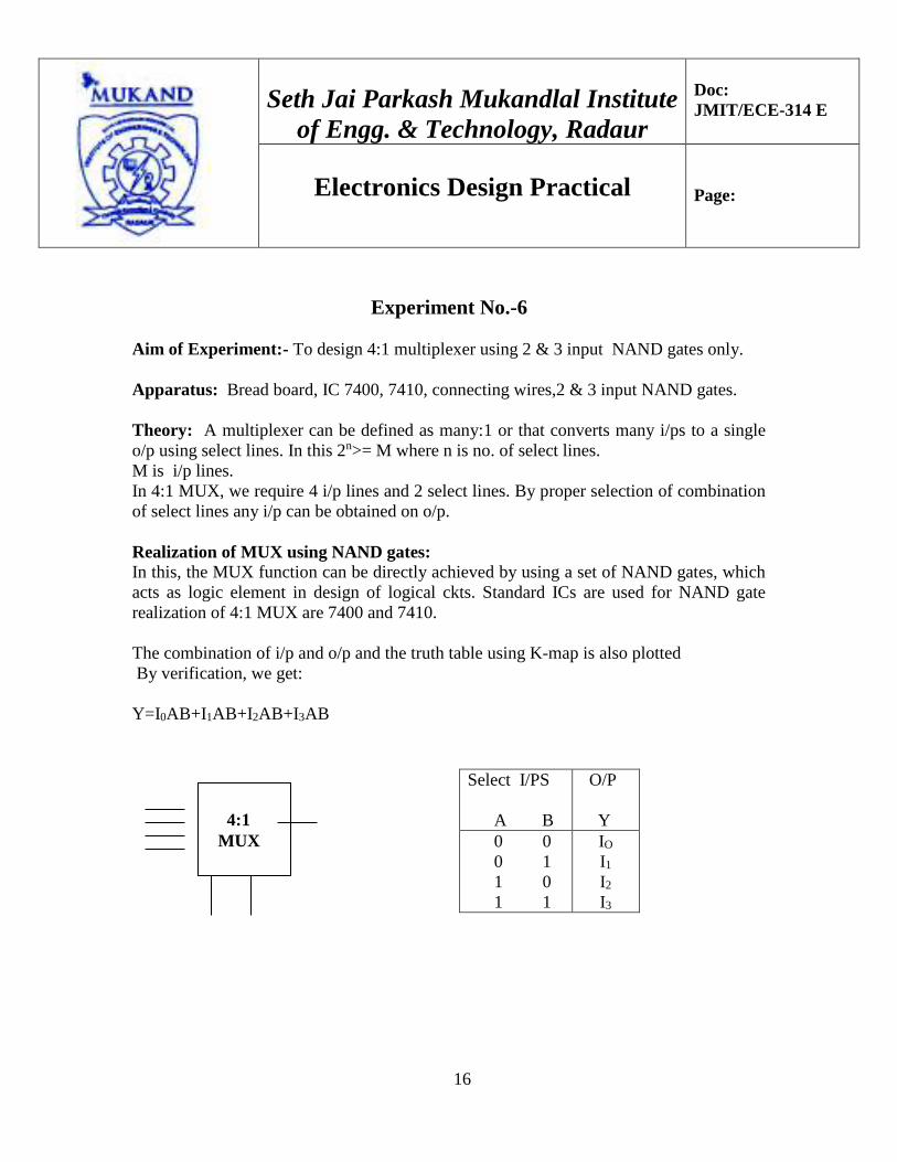
Experiment No.-6
Aim of Experiment:- To design 4:1 multiplexer using 2 & 3 input NAND gates only.
Apparatus: Bread board, IC 7400, 7410, connecting wires,2 & 3 input NAND gates.
Theory: A multiplexer can be defined as many:1 or that converts many i/ps to a single
o/p using select lines. In this 2n>= M where n is no. of select lines.
M is i/p lines.
In 4:1 MUX, we require 4 i/p lines and 2 select lines. By proper selection of combination
of select lines any i/p can be obtained on o/p.
Realization of MUX using NAND gates:
In this, the MUX function can be directly achieved by using a set of NAND gates, which
acts as logic element in design of logical ckts. Standard ICs are used for NAND gate
realization of 4:1 MUX are 7400 and 7410.
The combination of i/p and o/p and the truth table using K-map is also plotted
By verification, we get:
Y=I0AB+I1AB+I2AB+I3AB
Select I/PS
A B
O/P
Y
0 0
0 1
1 0
1 1
IO
I1
I2
I3
4:1
MUX

17
Seth Jai Parkash Mukandlal Institute
of Engg. & Technology, Radaur
Doc:
JMIT/ECE-314 E
Electronics Design Practical
Page:
Circuit Diagram:
Procedure
1 Make connection as shown in fig
2 Give logic 1 or logic 0 on s1 and s0 and give input on input lines
3 Check the o/p y by connecting to an LED
4 It will be according to the value of S1 and S0
5 Verify the truth table
Precautions:
1 Make the connection high
2 Give proper Vcc and ground to the correct pins of IC
3 Switch ON the power supply after making all connections
Result:
THE 4:1 MUX using NAND GATE have been realized.
0S
`1S
0I
1
1
0
I
S
S
2
1
0
I
S
S
3
1
0
I
S
S
Y
7400
74007410
7410
7410
7410
7410

18
Seth Jai Parkash Mukandlal Institute
of Engg. & Technology, Radaur
Doc:
JMIT/ECE-314 E
Electronics Design Practical
Page:
Experiment No.-7
Aim of Experiment- To design parallel parity bit generator.
Apparatus: EX-OR 7486, NOT 7404 ICs, connecting wires, breadboard, power supply.
Theory: A parity bit is a binary digit that is added to ensure that the number of bits with
value one in a given data is always even or odd.
Parity bit is used as simplest error detecting code. There are two types of parity bits even
parity bit and Odd parity bit. An even parity bit is set if the number of 1's in the given set
of bits are odd (To make the number of 1's even). An odd parity bit is set if number of 1's
in a given set of data is even (To make the number of 1's odd).
Using the parity bit single bit error can be detected in the receiver. If receiver finds any
change in the number of 1's this may request for retransmission of data.
Even parity system is generally designed using EX-OR gates and Odd parity system is
designed using EX-NOR gates. Checking of the parity bit may also be done by the gate
opposite to the gate through which parity was generated. Here we will design five bit
parity generator. Circuit diagram of the system is given in the fig.1.
Circuit Diagram:

19
Seth Jai Parkash Mukandlal Institute
of Engg. & Technology, Radaur
Doc:
JMIT/ECE-314 E
Electronics Design Practical
Page:
Observation Table:
INPUT EVEN PARITY BIT ODD PARITY BIT
Procedure:
1. To design the five bit Even/Odd parity system use ICs of Ex-OR and NOT
gates.
2. Connect the circuit as per the circuit diagram in the fig.1.
3. Connects the four i/p's.
4. Observe the o/p corresponding to the given i/p.
Precautions:
1. Connect the circuit carefully.
2. Connect the supply voltage to the IC's with in the range prescribed.
3. Keep away from live wire.
Result: Parallel parity bit generator is designed.

20
Seth Jai Parkash Mukandlal Institute
of Engg. & Technology, Radaur
Doc:
JMIT/ECE-314 E
Electronics Design Practical
Page:
Experiment No.-8
Aim of Experiment: To design digital to analog (D/A) converter using IC-741.
Apparatus: 741 IC, Resistors, connecting wires, breadboard, power supply, digital
multimeter etc.
Theory: A D/A converter is used when a binary data from a digital system is required to
be converted to analog form. A D/A converter in its simplest form use an OP-AMP and
R-2R ladder circuit.
Since number binary input is four this is called 4-bit converter. Because there is 16
combinations of binary i/ps therefore the analog o/p should have 16 possible levels of
o/p. Depending upon whether the switch is open or closed the binary weighted current
will be set up in the input resistors.
The sum of these current is equal to the current trough Rf which in turn is converted onto
a proportional o/p voltage when all switches are closed, the o/p will be maximum. the o/p
voltage equation is given by:-
V0=-Rf/16R (b0+ 2b1+ 4b2+ 8b3). Here we will design four bit D/A converter. Circuit
diagram of the system is given in the fig.1.
Circuit Diagram:

21
Seth Jai Parkash Mukandlal Institute
of Engg. & Technology, Radaur
Doc:
JMIT/ECE-314 E
Electronics Design Practical
Page:
Observation Table:
BINARY INPUT ANALOG OUTPUT
Observed Calculated
% error
Procedure:
1. Connect the circuit as per the circuit diagram in the fig.1.
2. Connects the four i/p's.
3. Observe the o/p corresponding to the given i/p.
4. Calculate the theoretical value of the o/p by using formula.
5. Calculate the errors in every observation.
Precautions:
1. Connect the circuit carefully.
2. Connect the supply voltage to the IC's with in the range prescribed.
3. Keep away from live wire.
Result: Digital to analog (D/A) converter using IC-741 is designed.

22
Seth Jai Parkash Mukandlal Institute
of Engg. & Technology, Radaur
Doc:
JMIT/ECE-314 E
Electronics Design Practical
Page:
Experiment No.-9
Aim of Experiment:- To design a digital frequency meter (0-999Hz) using IC-555 for
monoshot.
Apparatus: OP-AMP (IC-741), IC-555, resistances, capacitor, connecting wires, bread
board, power supplies, DMM (Digital Multimeter).
Circuit Diagram:

23
Seth Jai Parkash Mukandlal Institute
of Engg. & Technology, Radaur
Doc:
JMIT/ECE-314 E
Electronics Design Practical
Page:
THEORY: This audio frequency meter uses 555 IC as a monostable multivibrator (one-
shoot trigger). A monostable multivibrator can act as a frequency-to-voltage converter
because it produces a fixed pulse width; with the repetition rate/density is proportional to
the triggering input frequency. For resistor R1, because it set the measurement range, it’s
better to use a rotary switch to select different values for different ranges. For the ampere
meter, you can use both analog and digital ampere meter. A cheap dual-slope ADC
digital meter is suitable because its averaging characteristic, but a fast digital multimeter
can also be used although it may show some uncertainty because of their fast sampling.
Procedure:
1. Connect the circuit as per the circuit diagram in the fig.1.
2. Connect the i/p.
3. Observe the o/p corresponding to the given i/p.
Precautions:
1.Connect the circuit carefully. 2. Connect the supply voltage to the IC's with in the range prescribed.
3. Keep away from live wire.
Result: Digital frequency meter using IC 555 is designed.

24
Seth Jai Parkash Mukandlal Institute
of Engg. & Technology, Radaur
Doc:
JMIT/ECE-314 E
Electronics Design Practical
Page:
Experiment No.-10
Aim of Experiment To design a controller such that LEDs glow in a pair sequentially
using IC-7490 & LEDs.
Requirements: IC-7490, resistances, LEDs, connecting wires, bread board, power
supplies, IC-7497.
Circuit Diagram:
Theory:
This simple counter can be used to count pulses, as the basis for a customer
counter or for anything else that may be counted. The circuit accepts any TTL compatible
logic signal, and can be expanded easily. Resistors R1-R7 of 470 ohm is used as watt
resistors.7490 IC TTL act as BCD counter IC which counts the pulses. 7947 TTL act as
seven segment display driver IC with this leds will glow in a pair. Disp1ay is common
anode 7 segment LED display.

25
Seth Jai Parkash Mukandlal Institute
of Engg. & Technology, Radaur
Doc:
JMIT/ECE-314 E
Electronics Design Practical
Page:
Procedure:
1. Make the connection as per the ckt. diagram.
2. Apply input clock from clock generator.
3. At output LEDs will glow according to clock.
Observation: Controller using IC7490 is observed as led’s glow in a pair.
Precaution:
1. Connect the circuit carefully.
2. Connect the supply voltage to the IC's with in the range prescribed.
3. Keep away from live wire.
Result: Controller using IC-7490 is designed.
26
Seth Jai Parkash Mukandlal Institute
of Engg. & Technology, Radaur
Doc:
JMIT/ECE-314 E
Electronics Design Practical
Page:
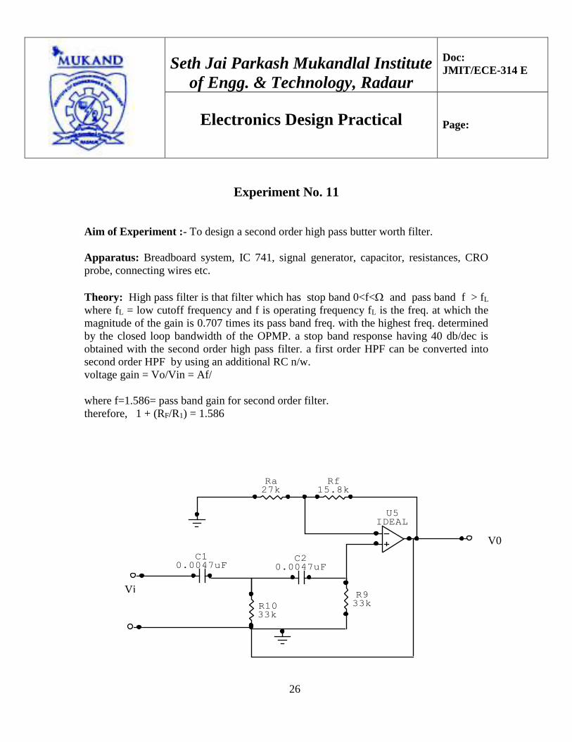
Experiment No. 11
Aim of Experiment :- To design a second order high pass butter worth filter.
Apparatus: Breadboard system, IC 741, signal generator, capacitor, resistances, CRO
probe, connecting wires etc.
Theory: High pass filter is that filter which has stop band 0<f< and pass band f > fL
where fL = low cutoff frequency and f is operating frequency fL is the freq. at which the
magnitude of the gain is 0.707 times its pass band freq. with the highest freq. determined
by the closed loop bandwidth of the OPMP. a stop band response having 40 db/dec is
obtained with the second order high pass filter. a first order HPF can be converted into
second order HPF by using an additional RC n/w.
voltage gain = Vo/Vin = Af/
where f=1.586= pass band gain for second order filter.
therefore, 1 + (RF/R1) = 1.586
C20.0047uF
C10.0047uF
R1033k
R933k
Rf15.8k
Ra27k
U5IDEAL
Vi
V0
27
Seth Jai Parkash Mukandlal Institute
of Engg. & Technology, Radaur
Doc:
JMIT/ECE-314 E
Electronics Design Practical
Page:
Procedure:
1. First of all choose value of cutoff freq. fL and let it be 1KHz .
2. To simplify design calculations, set R2=R3=Rand C2=C3=C
3. Choose the value of C<= 1 F.
4 Calculate the value of using en R=1/(2*pi* fL *C)
5. Now by using the relation RF =0.586R1 and for min. dc offset 2R= R1 || RF should be
satisfied. Choose value of R1<=100K and calculate the value of Rf.
6. After calculating the values of all components , take all components and assemble the
ckt on breadboard according to the ckt diagram.
7. Now pass signal of fixed amplitude and varying freq.
8. Note the output voltage at different signal frequencies.
9. Calculate the gain for different frequencies.
10. Plot the freq. response curve of HPF on semi log graph and locate fl.
Precautions:
1. Calculate values of resistance and capacitors accurately
2. Choose R1 and RF according to gain conditions
3. Make connections tight and clean
Observations:
S. No. Frequency O/P voltage (mV)
1
2
3
Result: The second order HP butter worth filter is designed using 74 1 and tested.
28
Seth Jai Parkash Mukandlal Institute
of Engg. & Technology, Radaur
Doc:
JMIT/ECE-314 E
Electronics Design Practical
Page:
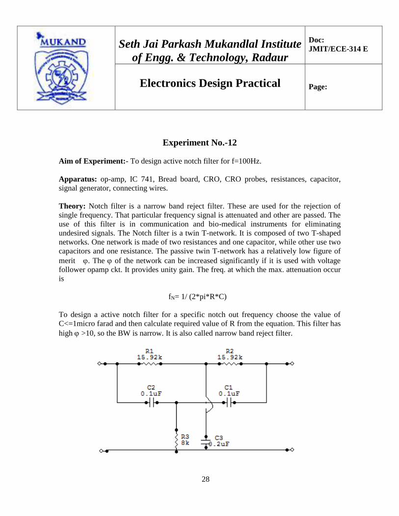
Experiment No.-12
Aim of Experiment:- To design active notch filter for f=100Hz.
Apparatus: op-amp, IC 741, Bread board, CRO, CRO probes, resistances, capacitor,
signal generator, connecting wires.
Theory: Notch filter is a narrow band reject filter. These are used for the rejection of
single frequency. That particular frequency signal is attenuated and other are passed. The
use of this filter is in communication and bio-medical instruments for eliminating
undesired signals. The Notch filter is a twin T-network. It is composed of two T-shaped
networks. One network is made of two resistances and one capacitor, while other use two
capacitors and one resistance. The passive twin T-network has a relatively low figure of
merit . The of the network can be increased significantly if it is used with voltage
follower opamp ckt. It provides unity gain. The freq. at which the max. attenuation occur
is
fN= 1/ (2*pi*R*C)
To design a active notch filter for a specific notch out frequency choose the value of
C<=1micro farad and then calculate required value of R from the equation. This filter has
high >10, so the BW is narrow. It is also called narrow band reject filter.

29
Seth Jai Parkash Mukandlal Institute
of Engg. & Technology, Radaur
Doc:
JMIT/ECE-314 E
Electronics Design Practical
Page:
+
-
V RL10k
C30.2uF
C20.1uF
C10.1uF
R38k
R215.92k
R115.92k
Procedure:
1. Set the ckt as shown in fig.
2. The ckt is established as per the design values of R&C.
3. Apply the input signal with the signal generator of varying frequency.
4. Observe the O/P on CRO for diff. frequency I/Ps.
5. Observe the O/P at which the O/P is zero i.e. notch frequency.
Observations:
S. No. Frequency O/P Amplitude
(V)
1
2
3
Result: The frequency at which the O/P is minimum can be find out.
30
Seth Jai Parkash Mukandlal Institute
of Engg. & Technology, Radaur
Doc:
JMIT/ECE-314 E
Electronics Design Practical
Page:
R3
R2
VBB
UJT
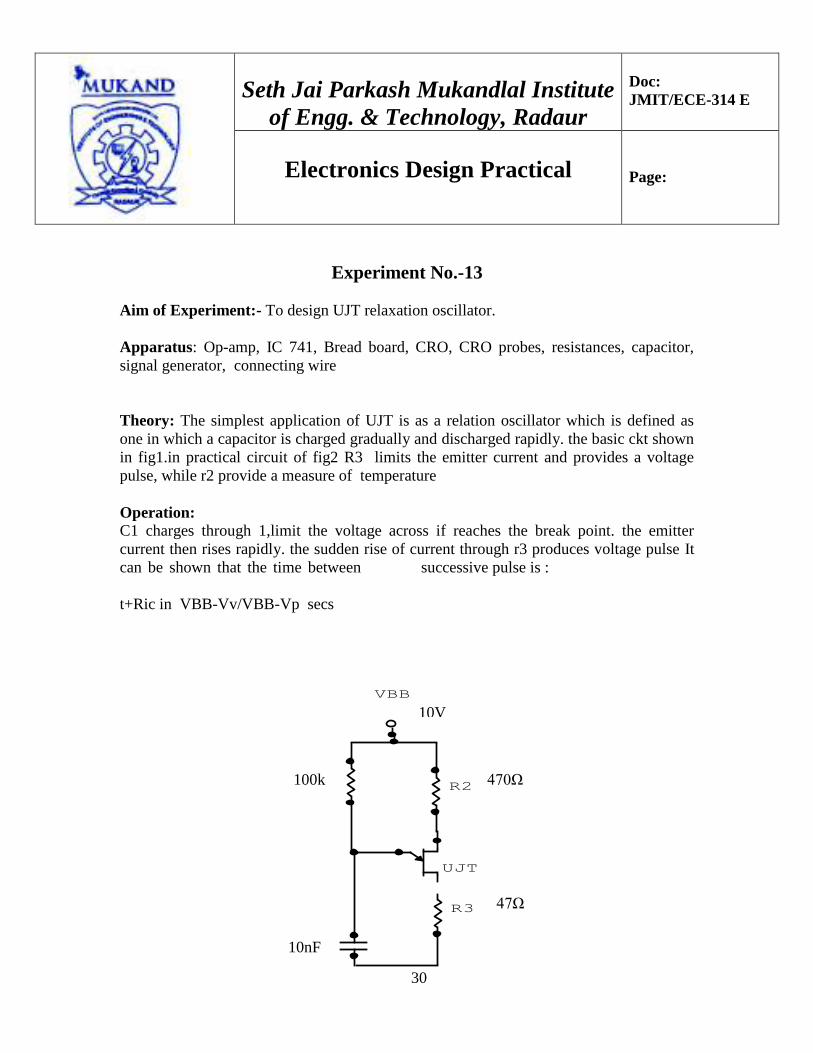
Experiment No.-13
Aim of Experiment:- To design UJT relaxation oscillator.
Apparatus: Op-amp, IC 741, Bread board, CRO, CRO probes, resistances, capacitor,
signal generator, connecting wire
Theory: The simplest application of UJT is as a relation oscillator which is defined as
one in which a capacitor is charged gradually and discharged rapidly. the basic ckt shown
in fig1.in practical circuit of fig2 R3 limits the emitter current and provides a voltage
pulse, while r2 provide a measure of temperature
Operation:
C1 charges through 1,limit the voltage across if reaches the break point. the emitter
current then rises rapidly. the sudden rise of current through r3 produces voltage pulse It
can be shown that the time between successive pulse is :
t+Ric in VBB-Vv/VBB-Vp secs
100k
10nF
470Ω
47Ω
10V
V

31
Seth Jai Parkash Mukandlal Institute
of Engg. & Technology, Radaur
Doc:
JMIT/ECE-314 E
Electronics Design Practical
Page:
Procedure:
1 Make the ckt. connection on breadboard
2 Switch on the power supply observe the o/p waveform on CRO
3 Measure the time period of waveform
Result:
The sawtooth generator using UJT 2N2646 is designed
32
Seth Jai Parkash Mukandlal Institute
of Engg. & Technology, Radaur
Doc:
JMIT/ECE-314 E
Electronics Design Practical
Page:
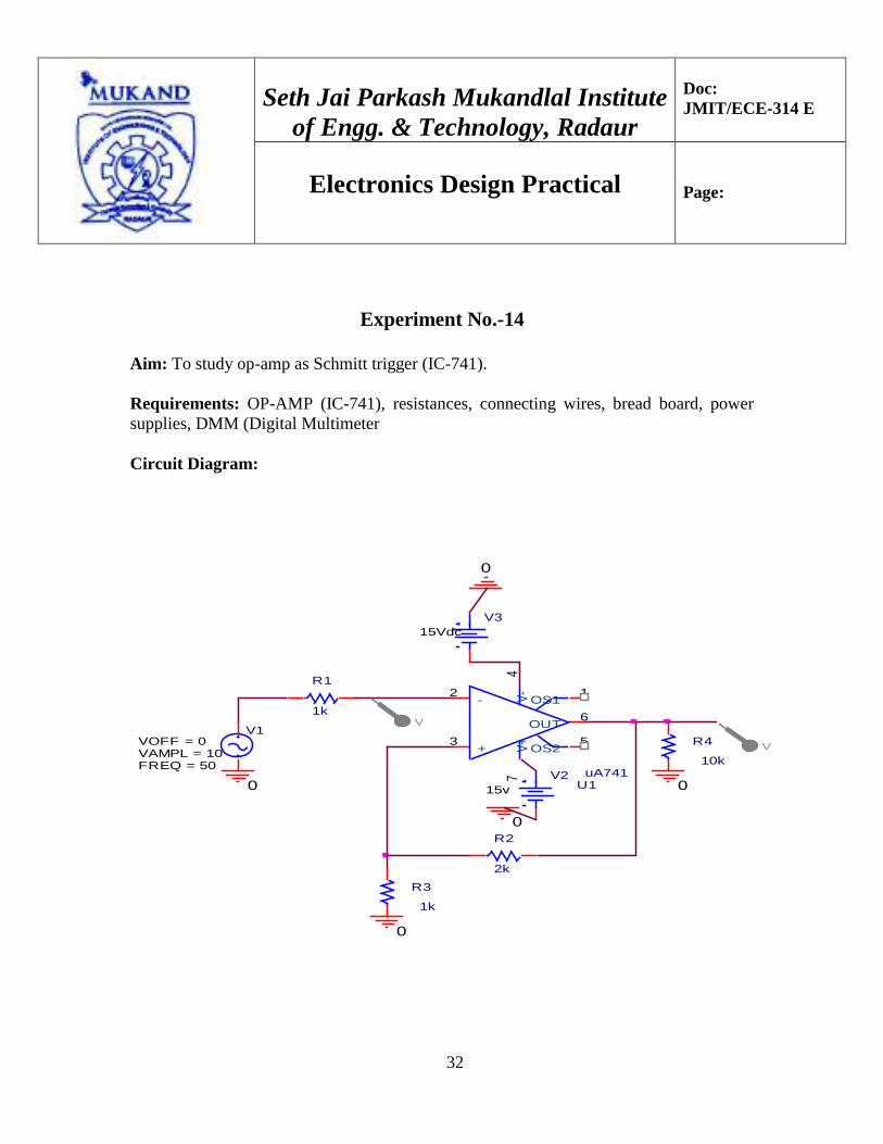
Experiment No.-14
Aim: To study op-amp as Schmitt trigger (IC-741).
Requirements: OP-AMP (IC-741), resistances, connecting wires, bread board, power
supplies, DMM (Digital Multimeter
Circuit Diagram:
0 U1uA741
3
2
74
6
1
5+
-
V+
V-
OUT
OS1
OS2
0
0
R1
1k
0
R2
2k
R3
1k
0
VR4
10k
V
V2
15v
V1
FREQ = 50VAMPL = 10VOFF = 0
V3
15Vdc

33
Seth Jai Parkash Mukandlal Institute
of Engg. & Technology, Radaur
Doc:
JMIT/ECE-314 E
Electronics Design Practical
Page:
Theory:
Schmitt trigger converts irregular waveforms to the square wave. The ckt. is
know as squaring ckt. The input voltage triggers the o\p voltage every time it exceeds the
certain level called upper threshold voltage is obtained by voltage divider R1-R2 where
voltage across R1is feed back to the +ve input that depends on the value and the polarity
of o\p voltage Vo.
The i\p voltage must slightly more +ve than Vo to cause the o\p to switch
from +Vsat to –Vsat. As long as Vin < Vout Vo is at +Vsat .
Procedure:
1. Connect the circuit as shown in fig.
2. Apply the input signal from function generator.
3. Make input supply at 100Hz.
4. Take the output from CRO.
5. Trace the input and output wave form on the paper.
Precautions:
i) Connections should be tight.
ii) Connection should be checked by instructor before switching on the supply.
Result: Op-Amp as Schmitt trigger has been studied.

34
Seth Jai Parkash Mukandlal Institute
of Engg. & Technology, Radaur
Doc:
JMIT/ECE-314 E
Electronics Design Practical
Page:
Experiment No.-15
Aim: To design 2nd order low pass Butterworth filter.
Requirements: OP-AMP (IC-741), resistances, capacitor, connecting wires, bread board,
power supplies, DMM (Digital Multimeter).
Circuit Diagram:

35
Seth Jai Parkash Mukandlal Institute
of Engg. & Technology, Radaur
Doc:
JMIT/ECE-314 E
Electronics Design Practical
Page:
Theory: A low pass filter is a ckt. This allows only the frequencies to pass which are
lower than higher cut off frequency (Fh). We can design the lpf of 2nd order using op-
amp.
The values of components are calculated with the following relations.
Designing:
1. Assume the value of higher cut off frequency.
2. We have relation Fh =
3. Select the suitable values of capacitors.
4. Now calculate the value of resistances for that particular frequency
5. Af = 1+Rf/R1
Procedure:
1. Connect the ckt. As shown in the figure.
2. Choose a particular frequency and calculate the value of components.
3. Set any value of bearable range of input voltage V. At that voltage find the output
voltage.
4. For different values of frequency note the output voltage and find the gain.
5. Graph is plotted b\w voltage gain and frequency.

36
Seth Jai Parkash Mukandlal Institute
of Engg. & Technology, Radaur
Doc:
JMIT/ECE-314 E
Electronics Design Practical
Page:
Observation Table:
Precautions:
i) Connections should be tight.
ii) Connection should be checked by instructor before switching on the supply.
Result: Second order Low pass butter worth filter has been designed.
Freq voltage gain

37
Seth Jai Parkash Mukandlal Institute
of Engg. & Technology, Radaur
Doc:
JMIT/ECE-314 E
Electronics Design Practical
Page:

38
Seth Jai Parkash Mukandlal Institute
of Engg. & Technology, Radaur
Doc:
JMIT/ECE-314 E
Electronics Design Practical
Page:

39
Seth Jai Parkash Mukandlal Institute
of Engg. & Technology, Radaur
Doc:
JMIT/ECE-314 E
Electronics Design Practical
Page:

40
Seth Jai Parkash Mukandlal Institute
of Engg. & Technology, Radaur
Doc:
JMIT/ECE-314 E
Electronics Design Practical
Page: